M S Engineering College Navarathna Agrahara, Sadahalli Post Off. Kempe Gowda International Airport Road, Bengaluru - 562110, Karnataka, India, LINEAR ICS AND COMMUNICATION LAB (15ECL48) Prepared By Azra Jeelani Associate Professor Department of Electronics and Communication Engineering M. S. Engineering College, Bengaluru – 562110

Welcome message from author
This document is posted to help you gain knowledge. Please leave a comment to let me know what you think about it! Share it to your friends and learn new things together.
Transcript
M S Engineering College Navarathna Agrahara, Sadahalli Post
Off. Kempe Gowda International Airport Road,
Bengaluru - 562110, Karnataka, India,
LINEAR ICS AND
COMMUNICATION LAB
(15ECL48)
Prepared By
Azra Jeelani
Associate Professor
Department of Electronics and Communication Engineering
M. S. Engineering College, Bengaluru – 562110
M S Engineering College
Vision
M.S.Engineering College shall blossom into a technical institution of national importance with global network.
Mission
• To be the leading institution in imparting Quality Engineering Education with value systems amongst students to face global challenges.
• To inculcate best engineering practices amongst students through quality education, creativity, innovation and entrepreneurial skills.
• To make the institute to be recognized as among the leading institutions imparting Quality Engineering Education; To produce world class professionals who possess knowledge, skills and necessary values that help them take challenges at a global level
Quality Policy
Striving for Excellence in Quality Engineering Education.
Our commitment to comply with mandatory requirements.
Continually improve the effectiveness and quality management system.
Our commitment to achieve total customer satisfaction by assuring successful completion of the degree with skill sets to solve the Engineering problems
By providing training at all the levels with placement assistance.
Use of modern technology and its conditional up gradation.
Participation of all the stakeholders to meet the expectations.

Department of Electronics and Communication Engineering
Vision
To equip students with strong technical knowledge by logical and innovative thinking in Electronics and Communication Engineering domain to meet expectations of the industry as well as society.
Mission
To educate a new generation of Electronics and Communication Engineers by providing them with a strong theoretical foundation, good design experience and exposure to research and development to meet ever changing and ever demanding needs of the Electronic Industry in particular, along with IT & other inter disciplinary fields in general.
Provide ethical and value based education by promoting activities addressing the societal needs.
To build up knowledge and skills of students to face the challenges across the globe with confidence and ease.
Quality Policy
Our quality policy is to develop an effective source of technical man power with the ability to adapt to an intellectually and technologically changing environment to contribute to the growth of nation with the participative efforts of the management, staff, students and industry while keeping up ethical and moral standards required
Program Outcomes:
1. Engineering knowledge: Apply the knowledge of mathematics, science, engineering fundamentals, and an engineering specialization to the solution of complex engineering problems.
2. Problem analysis: Identify, formulate, review research literature, and analyze complex engineering problems reaching substantiated conclusions using first principles of mathematics, natural sciences, and engineering sciences.
3. Design/development of solutions: Design solutions for complex engineering problems and design system components or processes that meet the specified needs with appropriate consideration for the public health and safety, and the cultural, societal, and environmental considerations.
4. Conduct investigations of complex problems: Use research-based knowledge and research methods including design of experiments, analysis and interpretation of data, and synthesis of the information to provide valid conclusions.
5. Modern tool usage: Create, select, and apply appropriate techniques, resources, and modern engineering and IT tools including prediction and modeling to complex engineering activities with an understanding of the limitations.
6. The engineer and society: Apply reasoning informed by the contextual knowledge to assess societal, health, safety, legal and cultural issues and the consequent responsibilities relevant to the professional engineering practice.
7. Environment and sustainability: Understand the impact of the professional engineering Solutions in societal and environmental contexts, and demonstrate the knowledge of, and need for sustainable development.
8. Ethics: Apply ethical principles and commit to professional ethics and responsibilities and norms of the engineering practice.
9. Individual and team work: Function effectively as an individual, and as a member or leader in diverse teams, and in multidisciplinary settings.
10. Communication: Communicate effectively on complex engineering activities with the engineering community and with society at large, such as, being able to comprehend and write effective reports and design documentation, make effective presentations, and give and receive clear instructions.
11. Project management and finance: Demonstrate knowledge and understanding of the engineering and management principles and apply these to one’s own work, as a member and leader in a team, to manage projects and in multidisciplinary environments.
12. Life-long learning: Recognize the need for, and have the preparation and ability to
engage in independent and life-long learning in the broadest context of technological change.
PSO-Program Specific Objectives
1. An ability to understand the concepts of basic Electronics & Communication Engineering and to apply them to various areas like Signal processing, VLSI, Embedded systems, Communication Systems, Digital & Analog Devices, etc.
2. An ability to solve complex Electronics and Communication Engineering problems, using latest hardware and software tools, along with analytical skills to arrive cost
effective and appropriate solutions.
3. Wisdom of social and environmental awareness along with ethical responsibility to have a successful career and to sustain passion and zeal for real-world applications using optimal resources as an Entrepreneur.
Program Educational Objectives
PEO I: To develop the ability among students to understand the concept of core electronics
subjects that will facilitate understanding of new technology.
PEO II: To embed a strong foundation in the engineering fundamentals to solve, analyze and
design real time engineering products.
PEO III: To give exposures to emerging edge technologies, adequate training and
opportunities to work as team on multidisciplinary projects with effective communication
skills and leadership qualities.
Linear ICs And Communication Lab [17ECL48] 2019-
20
Dept. of ECE M.S. Engineering College Page 1
LINEAR ICS AND COMMUNICATION LAB [17ECL48]
[As per Choice Based Credit System (CBCS) Scheme]
Laboratory Code 17ECL48 CIE Marks 40
Number of Lecture
Hours/Week
01Hr Tutorial (Instructions) +
02 Hours Laboratory
SEE Marks 60
RBT Level L1, L2, L3 Exam Hours 03
CREDITS – 02
Course objectives: This laboratory course enables students to design, Demonstrate and
Analyze instrumentation amplifier, filters, DAC, adder, differentiator and integrator circuits,
using op-amp. To design, Demonstrate and Analyze multivibrators and oscillator circuits using
Op-amp . To design, Demonstrate and Analyze analog systems for AM, FM and Mixer
operations. To design, Demonstrate and Analyze balance modulation and frequency synthesis.
To demonstrate and Analyze pulse sampling and flat top sampling.
NOTE:
1. Use discrete components to test and verify the logic gates. The IC umbers given are
suggestive. Any equivalent IC can be used.
2. For experiment No. 11 and 12 any open source or licensed simulation tool may be used.
Laboratory Experiments: Page
No
Marks
1. Design an instrumentation amplifier of a differential mode gain of A
using three amplifiers.
2. Design of RC Phase shift and Wien‘s bridge oscillators using Op-amp.
3. Design active second order Butterworth low pass and high pass filters.
4. Design 4 bit R – 2R Op-Amp Digital to Analog Converter (i) using 4 bit
binary input from toggle switches and (ii) by generating digital inputs
using mod-16 counter.
5. Design Adder, Integrator and Differentiator using Op-Amp.
6. Design of Monostable and Astable Multivibrator using 555 Timer
7. Demonstrate Pulse sampling, flat top sampling and reconstruction
8. Amplitude modulation using transistor/FET (Generation and detection).
9. Frequency modulation using IC 8038/2206 and demodulation.
10. Design BJT/FET Mixer.
11. DSBSC generation using Balance Modulator IC 1496/1596.
Linear ICs And Communication Lab [17ECL48] 2019-
20
Dept. of ECE M.S. Engineering College Page 2
12. Frequency synthesis using PLL.
Average = Total Marks scored / Total Number of Exp
Course Outcomes:
On the completion of this laboratory course, the students will be able to: Illustrate the pulse and
flat top sampling techniques using basic circuits. Demonstrate addition and integration using
linear ICs, and 555 timer operations to generate signals/pulses. Demonstrate AM and FM
operations and frequency synthesis. Design and illustrate the operation of instrumentation
amplifier, LPF, HPF, DAC and oscillators using linear IC.
Conduct of Practical Examination:
All laboratory experiments are to be included for practical examination. Students are allowed
to pick one experiment from the lot.Change of experiment is allowed only once and Marks
allotted to the procedure part to be made zero.
IA Evaluation
Record
maintenance
(weekly submission)
Conduction of Lab Internals Total
Write up Execution of the
required Result
Viva
10M 10M 15M 5M 40M
Linear ICs And Communication Lab [17ECL48] 2019-
20
Dept. of ECE M.S. Engineering College Page 3
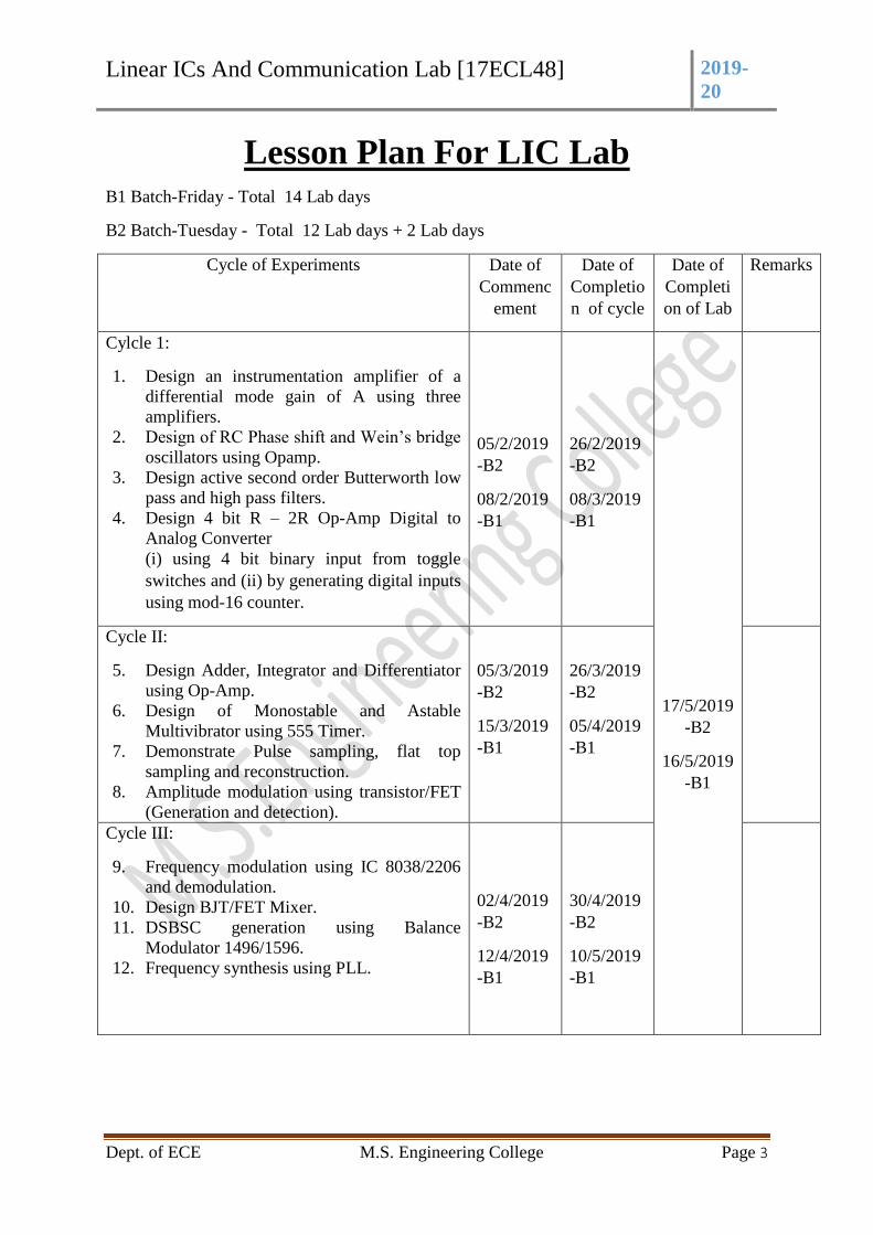
Lesson Plan For LIC Lab B1 Batch-Friday - Total 14 Lab days
B2 Batch-Tuesday - Total 12 Lab days + 2 Lab days
Cycle of Experiments Date of
Commenc
ement
Date of
Completio
n of cycle
Date of
Completi
on of Lab
Remarks
Cylcle 1:
1. Design an instrumentation amplifier of a
differential mode gain of A using three
amplifiers.
2. Design of RC Phase shift and Wein’s bridge
oscillators using Opamp.
3. Design active second order Butterworth low
pass and high pass filters.
4. Design 4 bit R – 2R Op-Amp Digital to
Analog Converter
(i) using 4 bit binary input from toggle
switches and (ii) by generating digital inputs
using mod-16 counter.
05/2/2019
-B2
08/2/2019
-B1
26/2/2019
-B2
08/3/2019
-B1
17/5/2019
-B2
16/5/2019
-B1
Cycle II:
5. Design Adder, Integrator and Differentiator
using Op-Amp.
6. Design of Monostable and Astable
Multivibrator using 555 Timer.
7. Demonstrate Pulse sampling, flat top
sampling and reconstruction.
8. Amplitude modulation using transistor/FET
(Generation and detection).
05/3/2019
-B2
15/3/2019
-B1
26/3/2019
-B2
05/4/2019
-B1
Cycle III:
9. Frequency modulation using IC 8038/2206
and demodulation.
10. Design BJT/FET Mixer.
11. DSBSC generation using Balance
Modulator 1496/1596.
12. Frequency synthesis using PLL.
02/4/2019
-B2
12/4/2019
-B1
30/4/2019
-B2
10/5/2019
-B1
Linear ICs And Communication Lab [17ECL48] 2019-
20
Dept. of ECE M.S. Engineering College Page 4
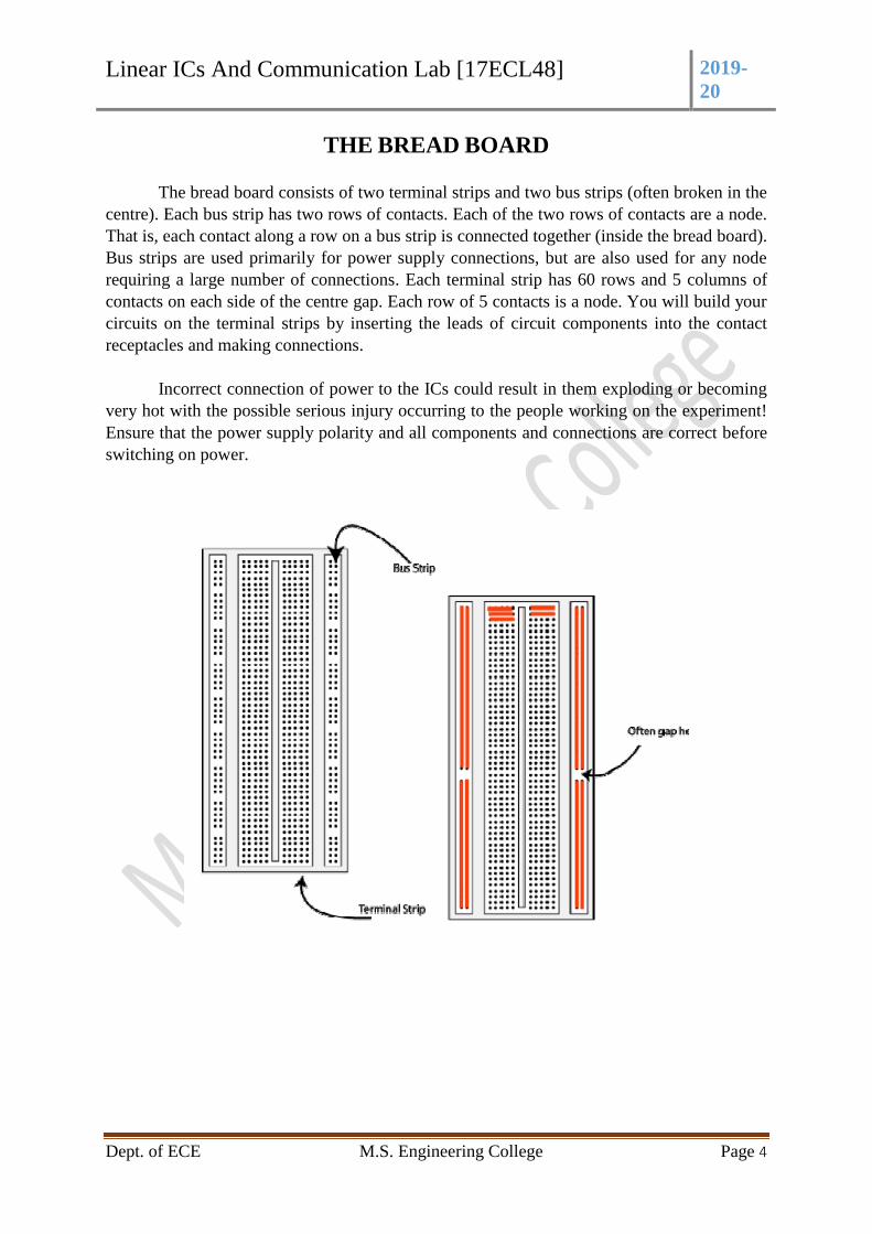
THE BREAD BOARD
The bread board consists of two terminal strips and two bus strips (often broken in the
centre). Each bus strip has two rows of contacts. Each of the two rows of contacts are a node.
That is, each contact along a row on a bus strip is connected together (inside the bread board).
Bus strips are used primarily for power supply connections, but are also used for any node
requiring a large number of connections. Each terminal strip has 60 rows and 5 columns of
contacts on each side of the centre gap. Each row of 5 contacts is a node. You will build your
circuits on the terminal strips by inserting the leads of circuit components into the contact
receptacles and making connections.
Incorrect connection of power to the ICs could result in them exploding or becoming
very hot with the possible serious injury occurring to the people working on the experiment!
Ensure that the power supply polarity and all components and connections are correct before
switching on power.
Linear ICs And Communication Lab [17ECL48] 2019-
20
Dept. of ECE M.S. Engineering College Page 5
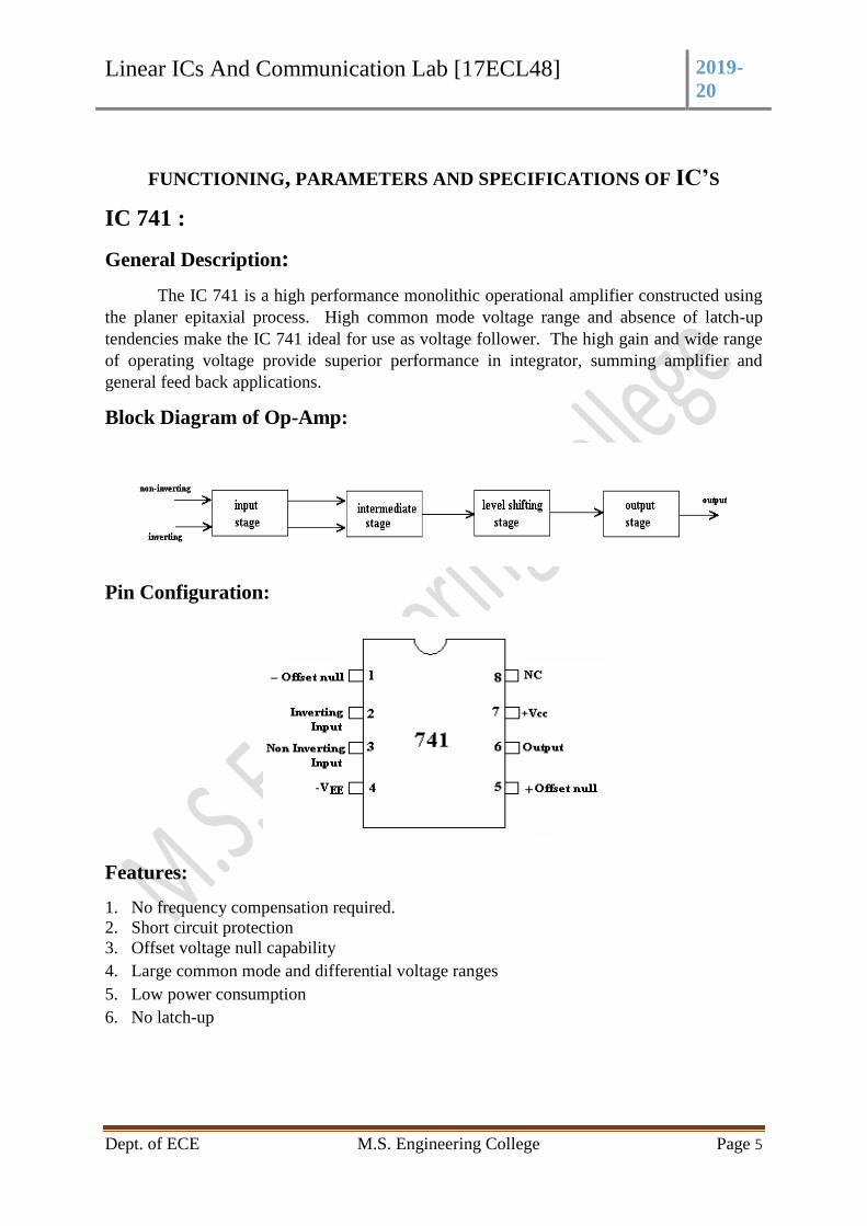
FUNCTIONING, PARAMETERS AND SPECIFICATIONS OF IC’S
IC 741 :
General Description:
The IC 741 is a high performance monolithic operational amplifier constructed using
the planer epitaxial process. High common mode voltage range and absence of latch-up
tendencies make the IC 741 ideal for use as voltage follower. The high gain and wide range
of operating voltage provide superior performance in integrator, summing amplifier and
general feed back applications.
Block Diagram of Op-Amp:
Pin Configuration:
Features:
1. No frequency compensation required.
2. Short circuit protection
3. Offset voltage null capability
4. Large common mode and differential voltage ranges
5. Low power consumption
6. No latch-up
Linear ICs And Communication Lab [17ECL48] 2019-
20
Dept. of ECE M.S. Engineering College Page 6
Specifications:
1. Voltage gain A = ∞ typically 2,00,000
2. I/P resistance RL = ∞ Ω, practically 2MΩ
3. O/P resistance R =0, practically 75Ω
4. Bandwidth = ∞ Hz. It can be operated at any frequency
5. Common mode rejection ratio = ∞
(Ability of op amp to reject noise voltage)
6. Slew rate= + ∞ V/μsec
(Rate of change of O/P voltage)
7. When V1 = V2, VD=0
8. Input offset voltage (Rs ≤ 10KΩ) max 6 mv
9. Input offset current = max , 200nA
10. Input bias current : 500nA
11. Input capacitance : typical value 1.4pF
12. Offset voltage adjustment range : ± 15mV
13. Input voltage range : ± 13V
14. Supply voltage rejection ratio : 150 μV/V
15. Output voltage swing: + 13V and – 13V for RL> 2KΩ
16. Output short-circuit current: 25mA
17. supply current: 28mA
18. Power consumption: 85mW
19. Transient response: rise time= 0.3 μs, Overshoot= 5%
Applications:
1. AC and DC amplifiers
2. Active filters
3. Oscillators
4. Comparators
5. Regulators
Linear ICs And Communication Lab [17ECL48] 2019-
20
Dept. of ECE M.S. Engineering College Page 7
IC 555:
Description: The operation of SE/NE 555 timer directly depends on its internal function. The three
equal resistors R1, R2, R3 serve as internal voltage divider for the source voltage. Thus
one-third of the source voltage VCC appears across each resistor.
Comparator is basically an Op amp which changes state when one of its inputs exceeds
the reference voltage. The reference voltage for the lower comparator is +1/3 VCC. If a
trigger pulse applied at the negative input of this comparator drops below +1/3 VCC, it
causes a change in state. The upper comparator is referenced at voltage +2/3 VCC. The
output of each comparator is fed to the input terminals of a flip flop.
The flip-flop used in the SE/NE 555 timer IC is a bistable multivibrator. This flip flop
changes states according to the voltage value of its input. Thus if the voltage at the
threshold terminal rises above +2/3 VCC, it causes upper comparator to cause flip-flop to
change its states. On the other hand, if the trigger voltage falls below +1/3 VCC, it causes
lower comparator to change its states. Thus the output of the flip flop is controlled by
the voltages of the two comparators. A change in state occurs when the threshold voltage
rises above +2/3 VCC or when the trigger voltage drops below +1/3 Vcc.
The output of the flip-flop is used to drive the discharge transistor and the output stage. A
high or positive flip-flop output turns on both the discharge transistor and the output
stage. The discharge transistor becomes conductive and behaves as a low resistance short
circuit to ground. The output stage behaves similarly. When the flip-flop output assumes
the low or zero states reverse action takes place i.e., the discharge transistor behaves as an
open circuit or positive VCC state. Thus the operational state of the discharge transistor
and the output stage depends on the voltage applied to the threshold and the trigger input
terminals.
Linear ICs And Communication Lab [17ECL48] 2019-
20
Dept. of ECE M.S. Engineering College Page 8
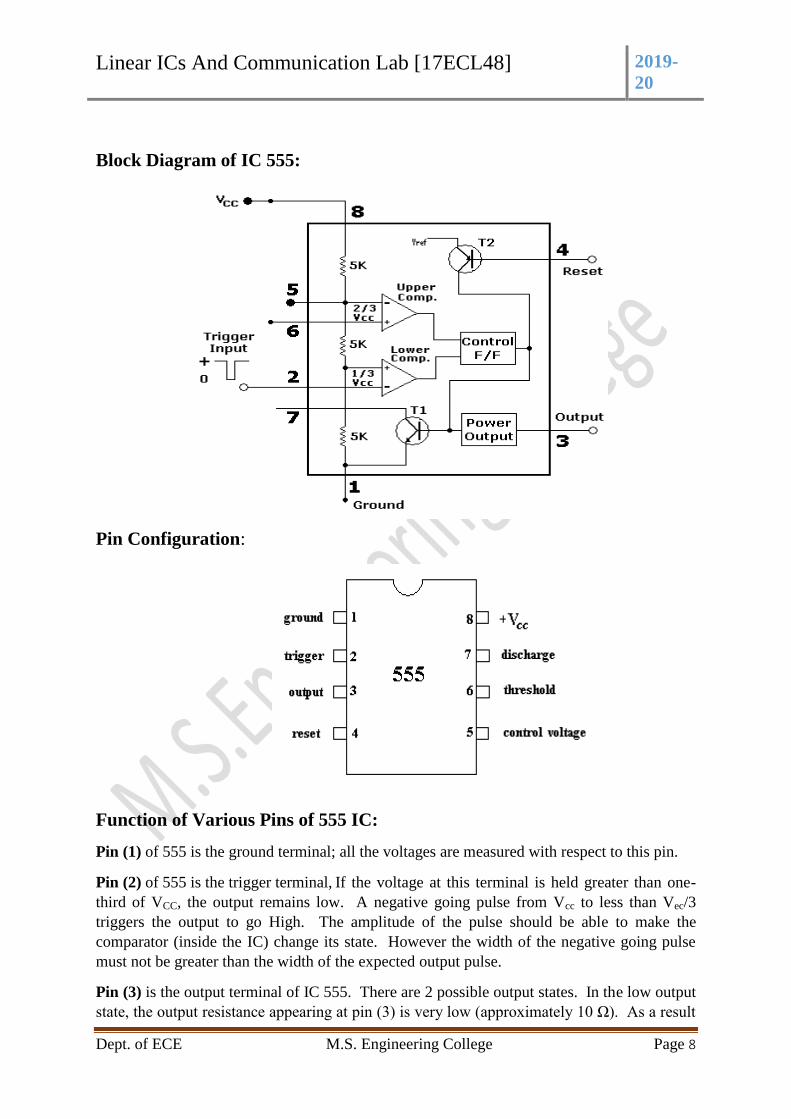
Block Diagram of IC 555:
Pin Configuration:
Function of Various Pins of 555 IC:
Pin (1) of 555 is the ground terminal; all the voltages are measured with respect to this pin.
Pin (2) of 555 is the trigger terminal, If the voltage at this terminal is held greater than one-
third of VCC, the output remains low. A negative going pulse from Vcc to less than Vec/3
triggers the output to go High. The amplitude of the pulse should be able to make the
comparator (inside the IC) change its state. However the width of the negative going pulse
must not be greater than the width of the expected output pulse.
Pin (3) is the output terminal of IC 555. There are 2 possible output states. In the low output
state, the output resistance appearing at pin (3) is very low (approximately 10 Ω). As a result
Linear ICs And Communication Lab [17ECL48] 2019-
20
Dept. of ECE M.S. Engineering College Page 9
the output current will goes to zero , if the load is connected from Pin (3) to ground , sink a
current I Sink (depending upon load) if the load is connected from Pin (3) to ground, and sinks
zero current if the load is connected between +VCC and Pin (3).
Pin (4) is the Reset terminal. When unused it is connected to +Vcc. Whenever the potential
of Pin (4) is drives below 0.4V, the output is immediately forced to low state. The reset
terminal enables the timer over-ride command signals at Pin (2) of the IC.
Pin (5) is the Control Voltage terminal. This can be used to alter the reference levels at which
the time comparators change state. A resistor connected from Pin (5) to ground can do the
job. Normally 0.01μF capacitor is connected from Pin (5) to ground. This capacitor
bypasses supply noise and does not allow it affect the threshold voltages.
Pin (6) is the threshold terminal. In both astable as well as monostable modes, a capacitor is
connected from Pin (6) to ground. Pin (6) monitors the voltage across the capacitor when it
charges from the supply and forces the already high O/p to Low when the capacitor reaches
+2/3 VCC.
Pin (7) is the discharge terminal. It presents an almost open circuit when the output is high
and allows the capacitor charge from the supply through an external resistor and presents an
almost short circuit when the output is low.
Pin (8) is the +Vcc terminal. 555 can operate at any supply voltage from +3 to +18V.
Features of 555 IC
1. The load can be connected to o/p in two ways i.e. between pin 3 & ground 1 or between
pin 3 & VCC (supply)
2. 555 can be reset by applying negative pulse, otherwise reset can be connected to +Vcc to
avoid false triggering.
3. An external voltage effects threshold and trigger voltages.
4. Timing from micro seconds through hours.
5. Monostable and bistable operation
6. Adjustable duty cycle
7. Output compatible with CMOS, DTL, TTL
8. High current output sink or source 200mA
9. High temperature stability
10. Trigger and reset inputs are logic compatible.
Specifications:
1. Operating temperature : SE 555-- -55oC to 125
oC
NE 555-- 0o to 70
oC
2. Supply voltage : +5V to +18V
3. Timing : μSec to Hours
4. Sink current : 200mA
5. Temperature stability : 50 PPM/oC change in temp or 0-005% /
oC.
Linear ICs And Communication Lab [17ECL48] 2019-
20
Dept. of ECE M.S. Engineering College Page 10
Applications:
1. Monostable and AstableMultivibrators
2. dc-ac converters
3. Digital logic probes
4. Waveform generators
5. Analog frequency meters
6. Tachometers
7. Temperature measurement and control
8. Infrared transmitters
9. Regulator & Taxi gas alarms etc.
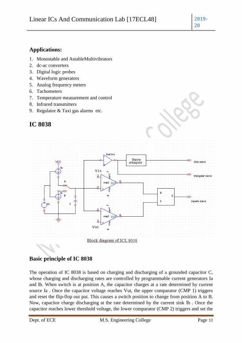
IC 8038
Basic principle of IC 8038
The operation of IC 8038 is based on charging and discharging of a grounded capacitor C,
whose charging and discharging rates are controlled by programmable current generators Ia
and Ib. When switch is at position A, the capacitor charges at a rate determined by current
source Ia . Once the capacitor voltage reaches Vut, the upper comparator (CMP 1) triggers
and reset the flip-flop out put. This causes a switch position to change from position A to B.
Now, capacitor charge discharging at the rate determined by the current sink Ib . Once the
capacitor reaches lower threshold voltage, the lower comparator (CMP 2) triggers and set the
Linear ICs And Communication Lab [17ECL48] 2019-
20
Dept. of ECE M.S. Engineering College Page 11
flip-flop output. This causes the switch position to change from position B to A. And this
cycle repeats. As a result, we get square wave at the output of Flip flop and triangular wave
across capacitor. The triangular wave is then passed through the on chip wave shaper to
generate sign wave. To allow automatic frequency controls, currents Ia and Ib are made
programmable through an external control voltage Bi. For equal magnitudes of Ia and Ib,
output waveforms are symmetrical conversely, when two currents are unequal, output
waveforms are asymmetrical. By making, one of the currents much larger than other we can
get saw tooth waveform across capacitor and rectangular waveform at the output of flip-flop.
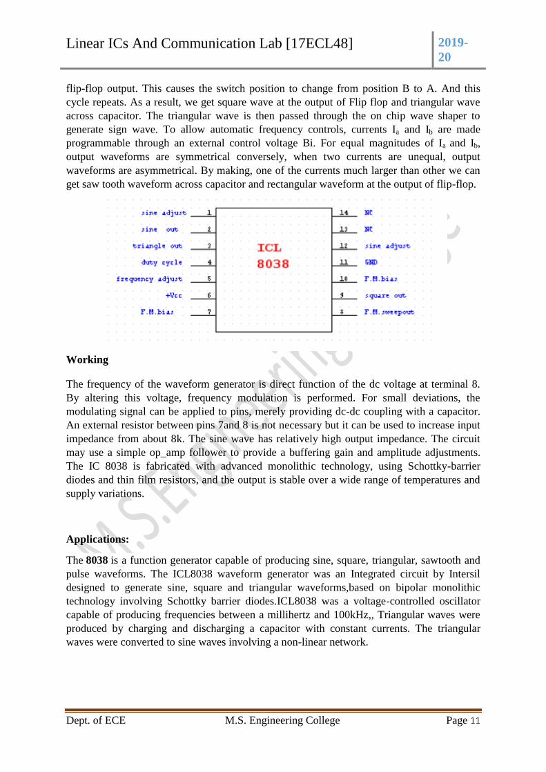
Working
The frequency of the waveform generator is direct function of the dc voltage at terminal 8.
By altering this voltage, frequency modulation is performed. For small deviations, the
modulating signal can be applied to pins, merely providing dc-dc coupling with a capacitor.
An external resistor between pins 7and 8 is not necessary but it can be used to increase input
impedance from about 8k. The sine wave has relatively high output impedance. The circuit
may use a simple op_amp follower to provide a buffering gain and amplitude adjustments.
The IC 8038 is fabricated with advanced monolithic technology, using Schottky-barrier
diodes and thin film resistors, and the output is stable over a wide range of temperatures and
supply variations.
Applications:
The 8038 is a function generator capable of producing sine, square, triangular, sawtooth and
pulse waveforms. The ICL8038 waveform generator was an Integrated circuit by Intersil
designed to generate sine, square and triangular waveforms,based on bipolar monolithic
technology involving Schottky barrier diodes.ICL8038 was a voltage-controlled oscillator
capable of producing frequencies between a millihertz and 100kHz,, Triangular waves were
produced by charging and discharging a capacitor with constant currents. The triangular
waves were converted to sine waves involving a non-linear network.
Linear ICs And Communication Lab [17ECL48] 2019-
20
Dept. of ECE M.S. Engineering College Page 12
Experiment No: 1 Date:
Design An Instrumentation Amplifier Of Differential Mode Gain Of A
Using Three Amplifiers
Aim: To design & test Instrumentation Amplifier for a given Gain and Determine the value
of CMRR.
Components required: Op-Amp 741,Resistor=10kohm,Multimeter, IC Bread Board
Theory:- Almost all types of sensors and transducers convert real world parameters like
light, temperature, weight etc into voltage values for our electronic systems to understand it.
The variation in this voltage level will help us in analyzing/measuring the real world
parameters, but in some applications like biomedical sensors this variation is very small (low-
level signals) and it is very important to keep track of even the minute variation to get reliable
data. In these applications an Instrumentation Amplifier is used.
An Instrumentation amplifier called as in-amps as the name suggests amplifies the variation
in voltage and provides a differential output like any other op-amps. But unlike a normal
amplifier the Instrumentation amplifiers will have high input impedance with good gain while
providing common mode noise rejection with fully differential inputs. Apart from normal op-
amps IC we have some special type of amplifiers for Instrumentation amplifier like INA114
IC. It is nothing more than few normal op-amps combined together for certain specific
applications.
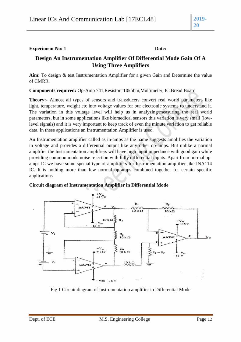
Circuit diagram of Instrumentation Amplifier in Differential Mode
Fig.1 Circuit diagram of Instrumentation amplifier in Differential Mode
Linear ICs And Communication Lab [17ECL48] 2019-
20
Dept. of ECE M.S. Engineering College Page 13
Tabular column:
V1 in volts V2 inVolts Vo(theoretical) in
volts
Vo(practical) in
volts
Ad=Vo/(V1-V2)
0.0
1.5
2.0
2.2
5.4
6.4
Average Ad =
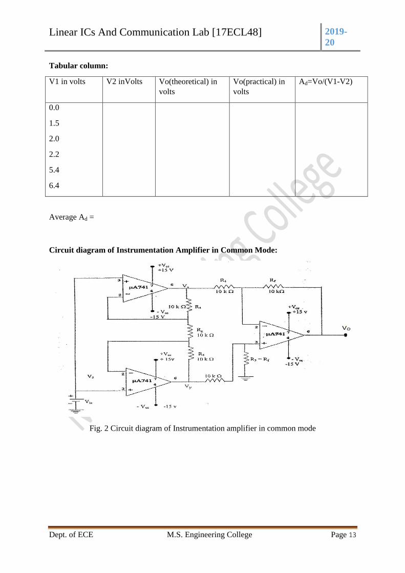
Circuit diagram of Instrumentation Amplifier in Common Mode:
Fig. 2 Circuit diagram of Instrumentation amplifier in common mode
Linear ICs And Communication Lab [17ECL48] 2019-
20
Dept. of ECE M.S. Engineering College Page 14
Tabular column:
Sl No VIN in Volts Vo(theoretical) in
volts
Vo(practical) in
volts
AC=Vo/Vin
Average Ac=
CMRR = 20log(Ad/Ac)
Design:
V0 = -
[ 1 +
](V1 – V2)
Differential gain,
Avf =
For Rf= R1 = R4 = Rg
Avf = -
( 1 +
)
V0= -3(V1 – V2) = - 3 Vd where Vd = (V1 – V2)
Procedure:
1. Circuit connections are made as shown in circuit diagram of figure 1 for Differential
Mode
2. Input V1 and V2 are varied in steps and Vo is measured using multimeter and
tabulated.
3. Differential Gain is calculated and verified with the designed gain.
4. For Common Mode connections are made as shown in circuit diagram of figure 2, V
is varied in steps ( 2V,3Vetc) . Vo is measured using multimeter.
5. Calculate the Common Mode Gain and Tabulate all the readings. Compute CMRR
from obtained differential and Common Mode Gain.
Result: Instrumentation amplified is understood by finding out the common mode gain,
differential gain and calculating common mode rejection ratio.
Linear ICs And Communication Lab [17ECL48] 2019-
20
Dept. of ECE M.S. Engineering College Page 15
Experiment No 2:
Design of RC Phase Shift and Wein’s Bridge Oscillators Using
Op-Amp.
Aim:To design and test RC Phaseshift & Wein’s bridge oscillator circuit using op-amp.
Components Reqd: Op-Amp 741,Resistor=10kohm,Multimeter, IC Bread Board
Theory:
A Wien bridge oscillator is a type of electronic oscillator that generates sine waves. It can
generate a large range of frequencies. The oscillator is based on a bridge circuit originally
developed by Max Wien in 1891 for the measurement of impedances.[1] The bridge
comprises four resistors and two capacitors. The oscillator can also be viewed as a positive
gain amplifier combined with a bandpass filter that provides positive feedback. Automatic
gain control, intentional non-linearity and incidental non-linearity limit the output amplitude
in various implementations of the oscillator.
RC phase-shift oscillator circuit can be built with a resistor as well as a capacitor. This circuit
offers the required phase shift with the feedback signal. They have outstanding frequency
strength and can give a clean sine wave for an extensive range of loads. Preferably an easy
RC network can be expected to include an o/p which directs the input with 90o. But in
actuality, the phase variation will be below this because the capacitor employed within the
circuit cannot be perfect.
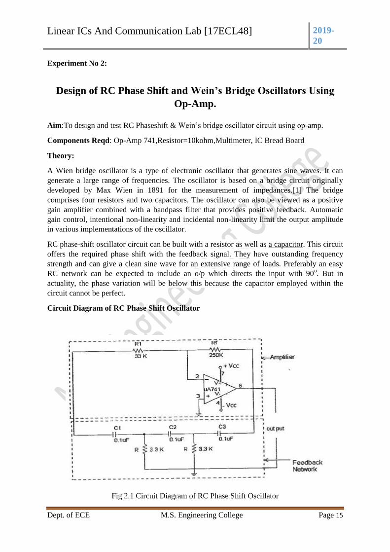
Circuit Diagram of RC Phase Shift Oscillator
Fig 2.1 Circuit Diagram of RC Phase Shift Oscillator
Linear ICs And Communication Lab [17ECL48] 2019-
20
Dept. of ECE M.S. Engineering College Page 16
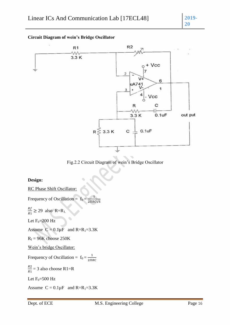
Circuit Diagram of wein’s Bridge Oscillator
Fig.2.2 Circuit Diagram of wein’s Bridge Oscillator
Design:
RC Phase Shift Oscillator:
Frequency of Oscillation = f0 =
√
29 also R=R1.
Let F0=200 Hz
Assume C = 0.1µF and R=R1=3.3K
Rf = 96K choose 250K
Wein’s bridge Oscillator:
Frequency of Oscillation = f0 =
= 3 also choose R1=R
Let F0=500 Hz
Assume C = 0.1µF and R=R1=3.3K
Linear ICs And Communication Lab [17ECL48] 2019-
20
Dept. of ECE M.S. Engineering College Page 17
R2=10K
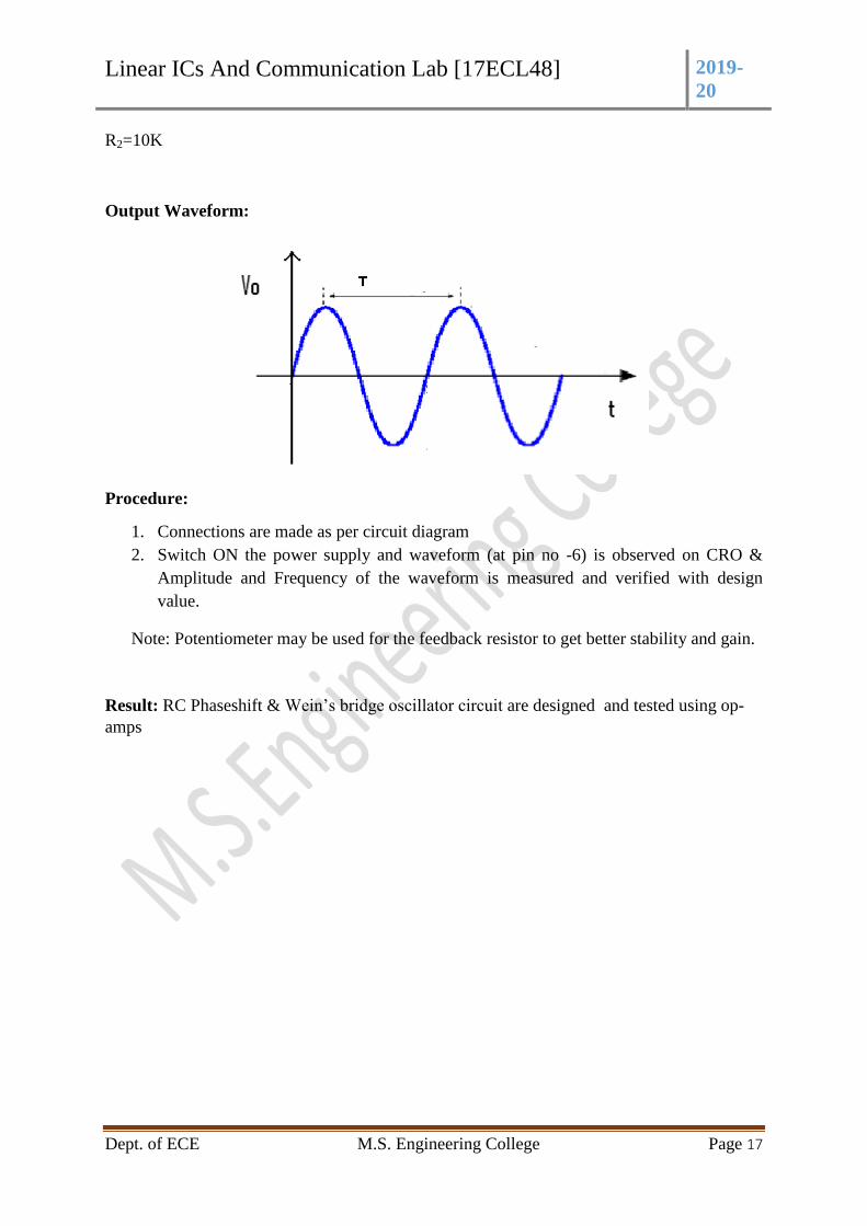
Output Waveform:
Procedure:
1. Connections are made as per circuit diagram
2. Switch ON the power supply and waveform (at pin no -6) is observed on CRO &
Amplitude and Frequency of the waveform is measured and verified with design
value.
Note: Potentiometer may be used for the feedback resistor to get better stability and gain.
Result: RC Phaseshift & Wein’s bridge oscillator circuit are designed and tested using op-
amps
Linear ICs And Communication Lab [17ECL48] 2019-
20
Dept. of ECE M.S. Engineering College Page 18
Experiment No 3:
Design Active Second Order Butterworth Low Pass and High Pass Filters
Aim:To draw the frequency response of an active LPF and HPF for a given cut-
off frequency.
Components Required: Op-Amp 741,Resistor=820Ω, 5.6KΩ, 10KΩ , Capacitor=0.1µF
Multimeter, IC Bread Board
Theory: A filter is a circuit designed to pass a specified band of frequencies while
attenuating all the signals outside the band. Filter network may be either Active or Passive.
Active filters consist of Active devices like op amplifier, transistor etc. Passive network
consist of passive device like Resistors, Capacitors, Inductors etc. There are 4 types of filters.
Low pass filter, High Pass filter, Band pass filter, Band Reject filter. Low pass filter: low pass
filter is a circuit which passes only low frequency signals and attenuate the high frequency
signal. An ideal low pass filter can be realized by multiplying a signal by rectangular
function. LPF is used to drive subwoofers and other type of loudspeaker to block high pitches
that they can efficiently broadcast. Radio transmitter use low pass filter to block harmonic
emissions which might cause interference with other communications. It can be used as an
integrator. It also plays a significant role in the sculpting of sound for electronics music as
created by synthesizers. A filter is a circuit designed to pass a specified band of frequencies
while attenuating all the signals outside the band. Filter network may be either Active or
Passive .High pass filter : High pass filter is a circuit which passes only High frequency
signals and attenuates the low frequency signal below cut-off frequency. amount of
attenuation varies from filter to filter. HPF is an opposite of low pass filter. A butter worth
filter provides a flat response in passband. higher the order of the filter faster the rate at which
the gain changes.eg for first order high pass filter gain raise at the rate of +20db/decade but
for second order it is 40db/decade. High pass filter with very low cutoff frequency can be
used to block DC signal which is undesired.
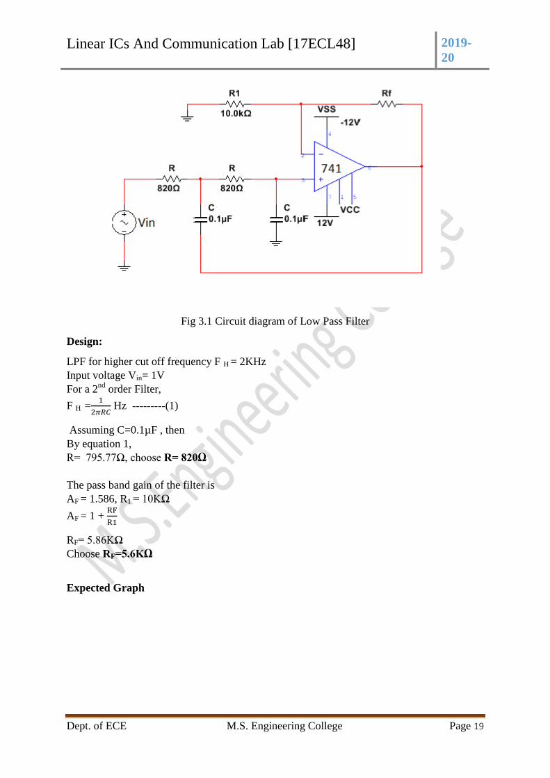
Circuit Diagram of LPF:
Linear ICs And Communication Lab [17ECL48] 2019-
20
Dept. of ECE M.S. Engineering College Page 19
Fig 3.1 Circuit diagram of Low Pass Filter
Design:
LPF for higher cut off frequency F H = 2KHz
Input voltage Vin= 1V
For a 2nd
order Filter,
F H =
Hz ---------(1)
Assuming C=0.1µF , then
By equation 1,
R= 795.77Ω, choose R= 820Ω
The pass band gain of the filter is
AF = 1.586, R1 = 10KΩ
AF = 1 +
RF= 5.86KΩ
Choose RF=5.6KΩ
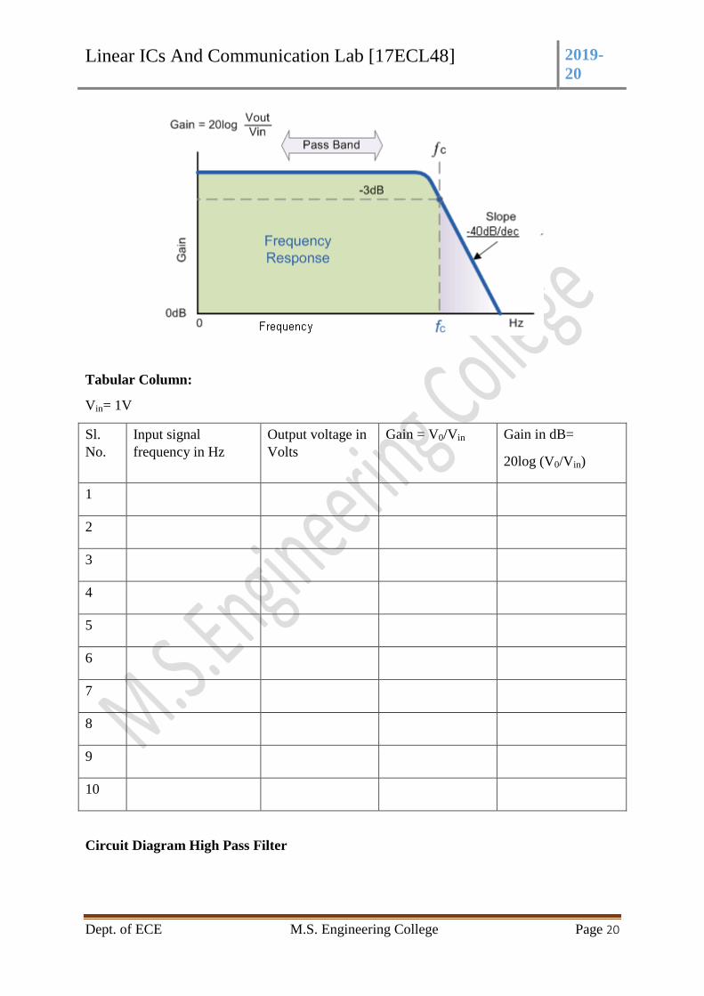
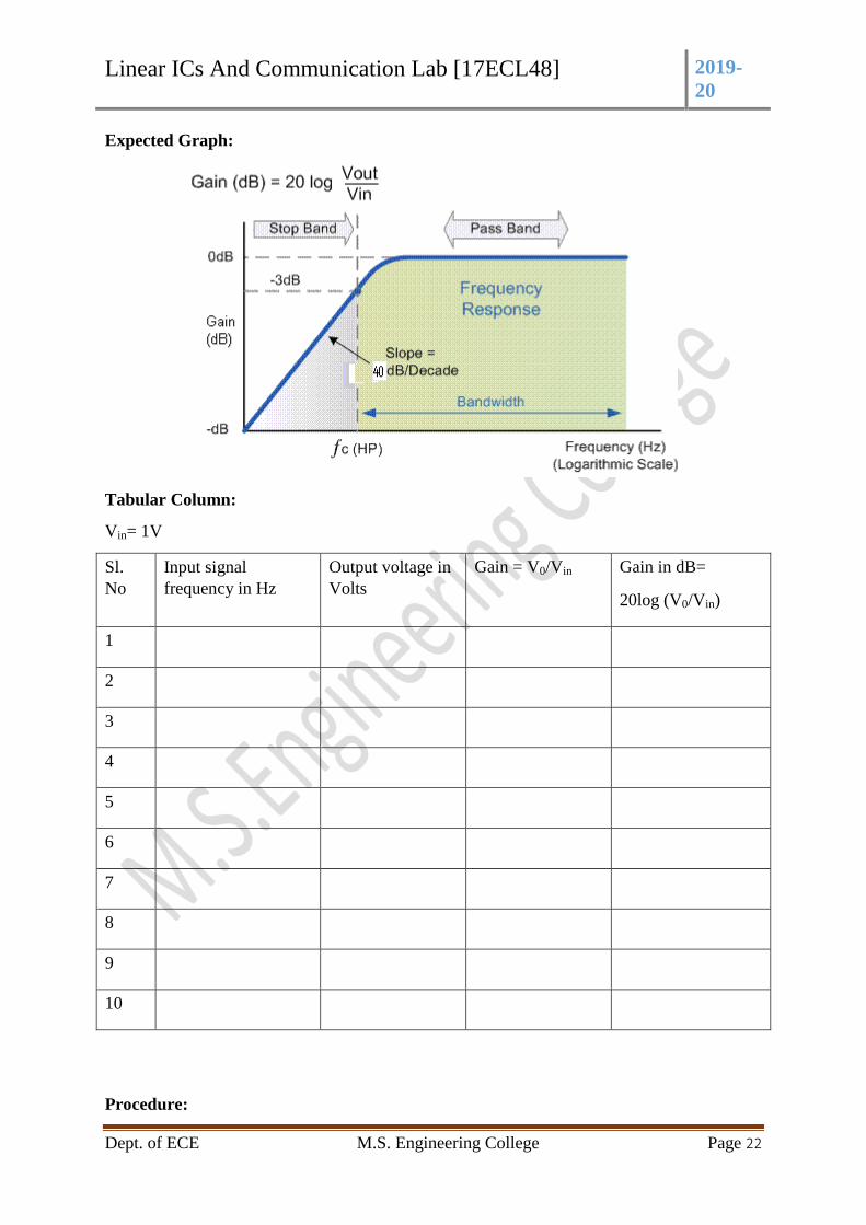
Expected Graph
Linear ICs And Communication Lab [17ECL48] 2019-
20
Dept. of ECE M.S. Engineering College Page 20
Tabular Column:
Vin= 1V
Sl.
No.
Input signal
frequency in Hz
Output voltage in
Volts
Gain = V0/Vin Gain in dB=
20log (V0/Vin)
1
2
3
4
5
6
7
8
9
10
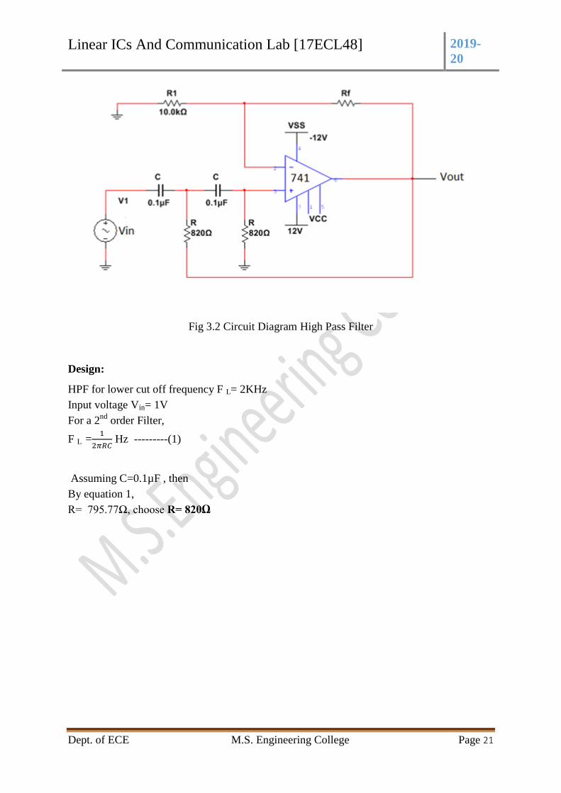
Circuit Diagram High Pass Filter
Linear ICs And Communication Lab [17ECL48] 2019-
20
Dept. of ECE M.S. Engineering College Page 21
Fig 3.2 Circuit Diagram High Pass Filter
Design:
HPF for lower cut off frequency F L= 2KHz
Input voltage Vin= 1V
For a 2nd
order Filter,
F L =
Hz ---------(1)
Assuming C=0.1µF , then
By equation 1,
R= 795.77Ω, choose R= 820Ω
Linear ICs And Communication Lab [17ECL48] 2019-
20
Dept. of ECE M.S. Engineering College Page 22
Expected Graph:
Tabular Column:
Vin= 1V
Sl.
No
Input signal
frequency in Hz
Output voltage in
Volts
Gain = V0/Vin Gain in dB=
20log (V0/Vin)
1
2
3
4
5
6
7
8
9
10
Procedure:
Linear ICs And Communication Lab [17ECL48] 2019-
20
Dept. of ECE M.S. Engineering College Page 23
1. Connections are made as shown in the Fig 3.1
2. Set the input voltage to 1v.
3. By varying the frequency of input from Hz range to KHz range, note the frequency
and the corresponding output voltage across pin 6 of the op amp with respect to the
ground.
4. Tabulate the readings in the tabular column.
5. Calculate gain in dB and Plot the frequency response on semi log sheet.
6. Find the cut off frequency using graph and compare it with the theoretical value.
Applications : Active lowpass filters are often used in audio/video ,avionics, automotives,
commercial and communications, computers and data acquisition, industrial, medical or
military applications. Some devices are also used in portable devices as personal digital
assistants and cell phones.
Result: The circuit has been verified for cut off frequency of 1khz for Roll off factor = -
40dB/decade
Linear ICs And Communication Lab [17ECL48] 2019-
20
Dept. of ECE M.S. Engineering College Page 24
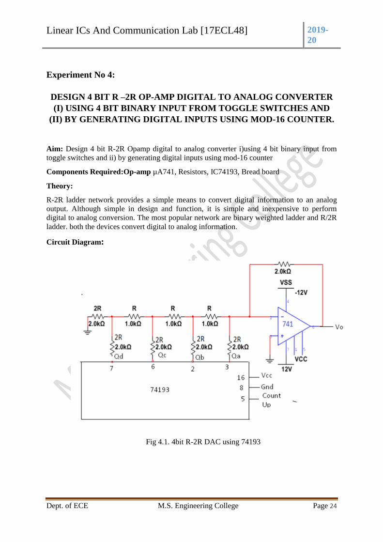
Experiment No 4:
DESIGN 4 BIT R –2R OP-AMP DIGITAL TO ANALOG CONVERTER
(I) USING 4 BIT BINARY INPUT FROM TOGGLE SWITCHES AND
(II) BY GENERATING DIGITAL INPUTS USING MOD-16 COUNTER.
Aim: Design 4 bit R-2R Opamp digital to analog converter i)using 4 bit binary input from
toggle switches and ii) by generating digital inputs using mod-16 counter
Components Required:Op-amp µA741, Resistors, IC74193, Bread board
Theory:
R-2R ladder network provides a simple means to convert digital information to an analog
output. Although simple in design and function, it is simple and inexpensive to perform
digital to analog conversion. The most popular network are binary weighted ladder and R/2R
ladder. both the devices convert digital to analog information.
Circuit Diagram:
Fig 4.1. 4bit R-2R DAC using 74193
Linear ICs And Communication Lab [17ECL48] 2019-
20
Dept. of ECE M.S. Engineering College Page 25
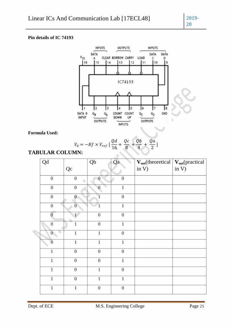
Pin details of IC 74193
Formula Used:
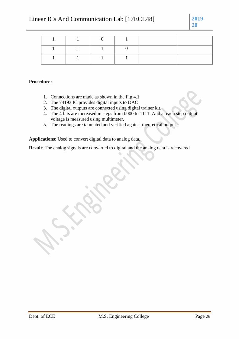
TABULAR COLUMN:
Qd
Qc
Qb Qa Vout(theoretical
in V)
Vout(practical
in V)
0 0 0 0
0 0 0 1
0 0 1 0
0 0 1 1
0 1 0 0
0 1 0 1
0 1 1 0
0 1 1 1
1 0 0 0
1 0 0 1
1 0 1 0
1 0 1 1
1 1 0 0
Linear ICs And Communication Lab [17ECL48] 2019-
20
Dept. of ECE M.S. Engineering College Page 26
1 1 0 1
1 1 1 0
1 1 1 1
Procedure:
1. Connections are made as shown in the Fig.4.1
2. The 74193 IC provides digital inputs to DAC
3. The digital outputs are connected using digital trainer kit.
4. The 4 bits are increased in steps from 0000 to 1111. And at each step output
voltage is measured using multimeter.
5. The readings are tabulated and verified against theoretical output.
Applications: Used to convert digital data to analog data.
Result: The analog signals are converted to digital and the analog data is recovered.
Linear ICs And Communication Lab [17ECL48] 2019-
20
Dept. of ECE M.S. Engineering College Page 27
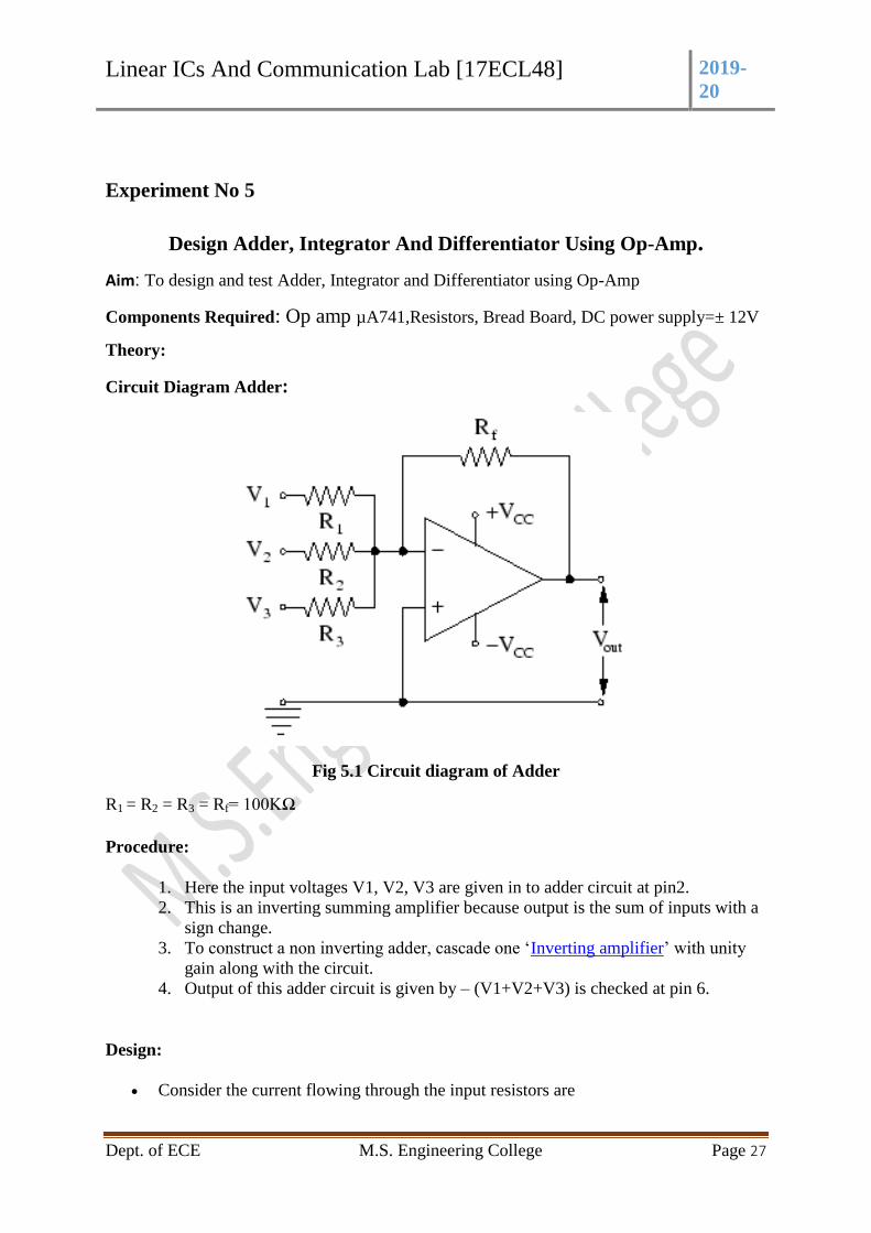
Experiment No 5
Design Adder, Integrator And Differentiator Using Op-Amp.
Aim: To design and test Adder, Integrator and Differentiator using Op-Amp
Components Required: Op amp µA741,Resistors, Bread Board, DC power supply=± 12V
Theory:
Circuit Diagram Adder:
Fig 5.1 Circuit diagram of Adder
R1 = R2 = R3 = Rf= 100KΩ
Procedure:
1. Here the input voltages V1, V2, V3 are given in to adder circuit at pin2.
2. This is an inverting summing amplifier because output is the sum of inputs with a
sign change.
3. To construct a non inverting adder, cascade one ‘Inverting amplifier’ with unity
gain along with the circuit.
4. Output of this adder circuit is given by – (V1+V2+V3) is checked at pin 6.
Design:
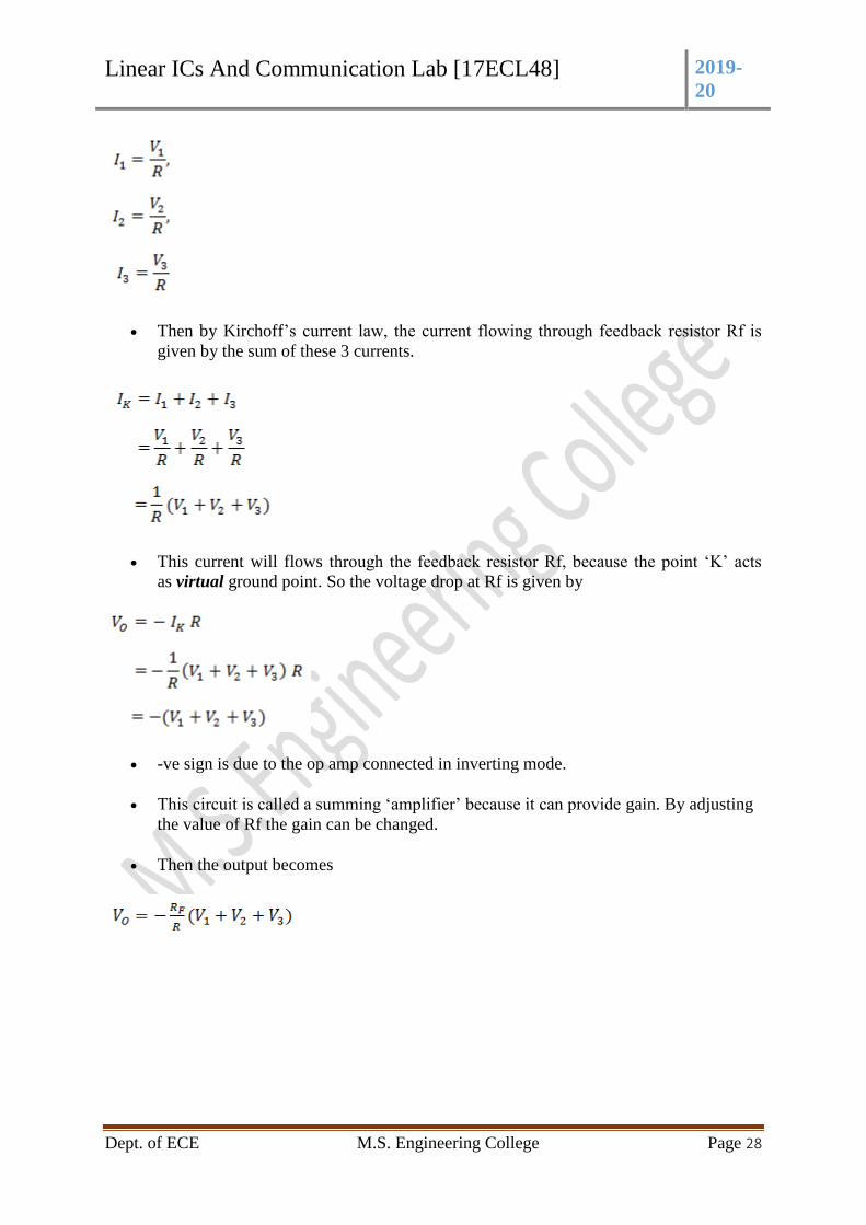
Consider the current flowing through the input resistors are
Linear ICs And Communication Lab [17ECL48] 2019-
20
Dept. of ECE M.S. Engineering College Page 28
Then by Kirchoff’s current law, the current flowing through feedback resistor Rf is
given by the sum of these 3 currents.
This current will flows through the feedback resistor Rf, because the point ‘K’ acts
as virtual ground point. So the voltage drop at Rf is given by
-ve sign is due to the op amp connected in inverting mode.
This circuit is called a summing ‘amplifier’ because it can provide gain. By adjusting
the value of Rf the gain can be changed.
Then the output becomes
Linear ICs And Communication Lab [17ECL48] 2019-
20
Dept. of ECE M.S. Engineering College Page 29
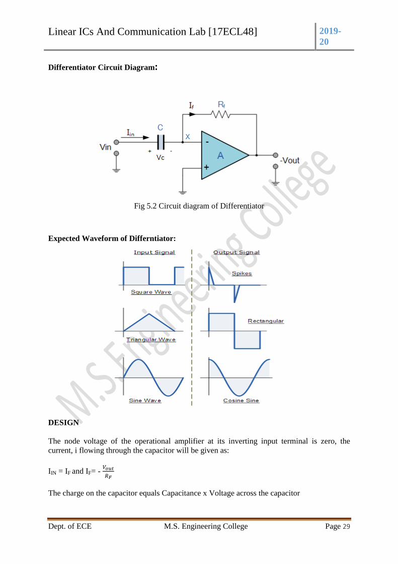
Differentiator Circuit Diagram:
Fig 5.2 Circuit diagram of Differentiator
Expected Waveform of Differntiator:
DESIGN
The node voltage of the operational amplifier at its inverting input terminal is zero, the
current, i flowing through the capacitor will be given as:
IIN = IF and IF= -
The charge on the capacitor equals Capacitance x Voltage across the capacitor
Linear ICs And Communication Lab [17ECL48] 2019-
20
Dept. of ECE M.S. Engineering College Page 30
Q = C * VIN
The rate of change of this charge is:
= C
butdQ/dt is the capacitor current,i
IIN =C
= IF
i.e, -
= C
from which we have an ideal voltage output for the op-amp differentiator is given as:
VOUT = - RF C
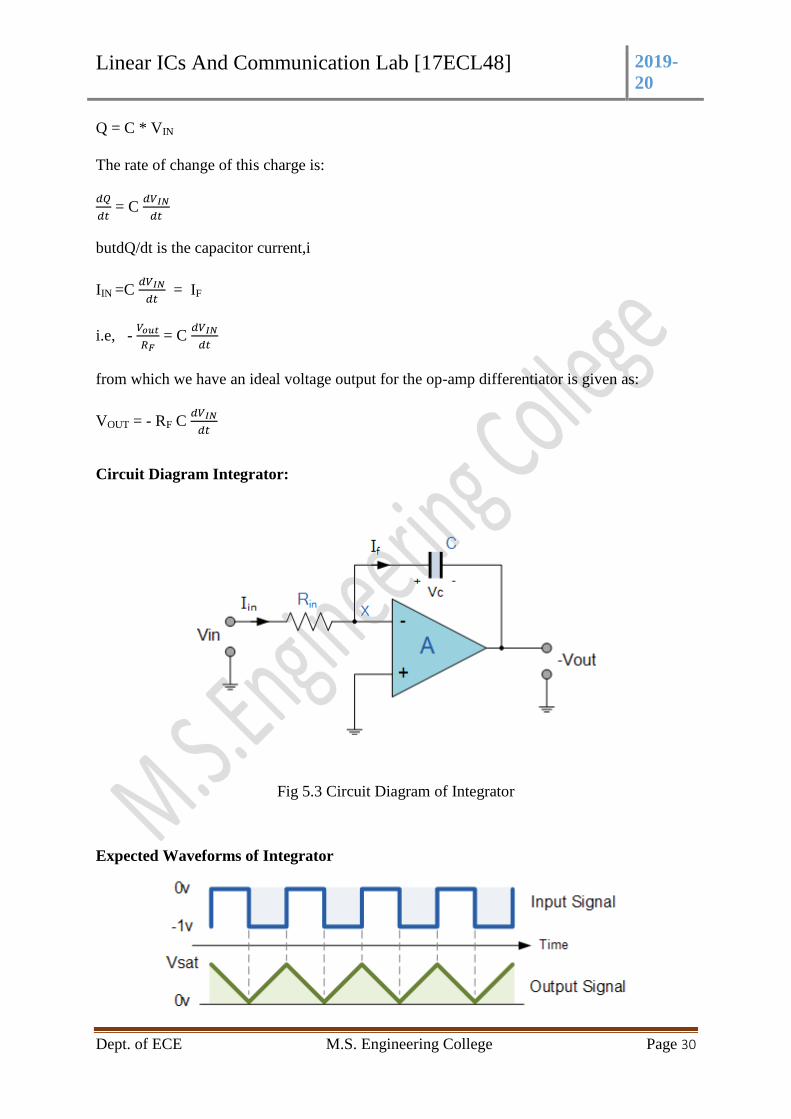
Circuit Diagram Integrator:
Fig 5.3 Circuit Diagram of Integrator
Expected Waveforms of Integrator
Linear ICs And Communication Lab [17ECL48] 2019-
20
Dept. of ECE M.S. Engineering College Page 31
Design
The voltage on the plates of a capacitor is equal to the charge on the capacitor divided by its
capacitance giving Q/C. Then the voltage across the capacitor is output Vout therefore: -
Vout = Q/C. If the capacitor is charging and discharging, the rate of charge of voltage across
the capacitor is given as:
VC =
, VC = VX – Vout = 0 – Vout
i.e, -
=
=
But dQ/dt is electric current and since the node voltage of the integrating op-amp at its
inverting input terminal is zero, X = 0, the input current I(in) flowing through the input
resistor, Rin is given as:
IIN =
=
The current flowing through the feedback capacitor C is given as:
If = C
= C
=
=
Assuming that the input impedance of the op-amp is infinite (ideal op-amp), no current flows
into the op-amp terminal. Therefore, the nodal equation at the inverting input terminal is
given as:
IIN = If =
=
i.e,
*
= 1
From which we derive an ideal voltage output for the Op-amp Integrator as:
Vout = -
∫
= - ∫
To simplify the math’s a little, this can also be re-written as:
Vout = -
Where ω = 2πƒ and the output voltage Vout is a constant 1/RC times the integral of the input
voltage Vin with respect to time. The minus sign ( – ) indicates a 180o phase shift because the
input signal is connected directly to the inverting input terminal of the op-amp.
Result:
Linear ICs And Communication Lab [17ECL48] 2019-
20
Dept. of ECE M.S. Engineering College Page 32
Experiment No 6
DESIGN OF MONOSTABLE AND ASTABLE MULTIVIBRATOR
USING 555 TIMER
Monostable Multivibrator
Aim: To design and test a monostable multivibrator using IC 555 timer.
Components Required: Timer IC 555, Resistors, Capacitors, Bread Board, DC Power
Supply
Theory: A monostable multivibrator (MMV) often called a one-shot multivibrator, is a pulse
generator circuit in which the duration of the pulse is determined by the R-C
network,connected externally to the 555 timer. In such a vibrator, one state of output is stable
while the other is quasi-stable (unstable). For auto-triggering of output from quasi-stable state
to stable state energy is stored by an externally connected capacitor C to a reference level.
The time taken in storage determines the pulse width. The transition of output from stable
state to quasi-stable state is accomplished by external triggering. The schematic of a 555
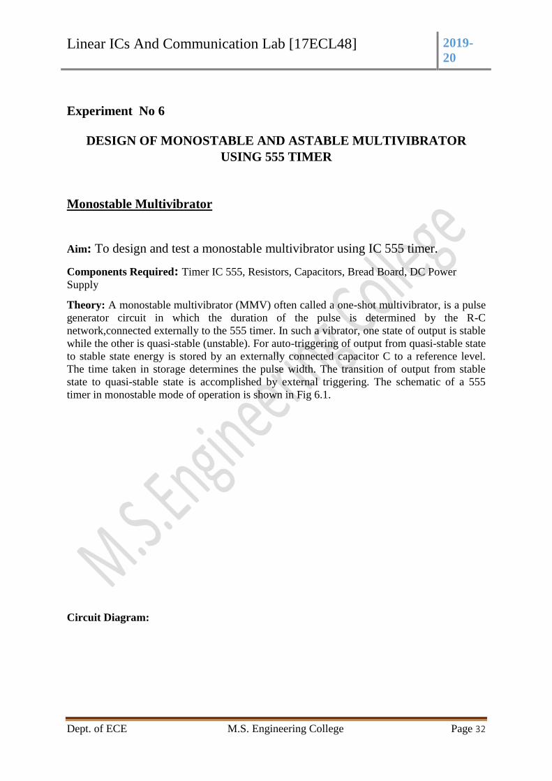
timer in monostable mode of operation is shown in Fig 6.1.
Circuit Diagram:
Linear ICs And Communication Lab [17ECL48] 2019-
20
Dept. of ECE M.S. Engineering College Page 33
Fig 6.1 Circuit Diagram of Monostable Multivibrator
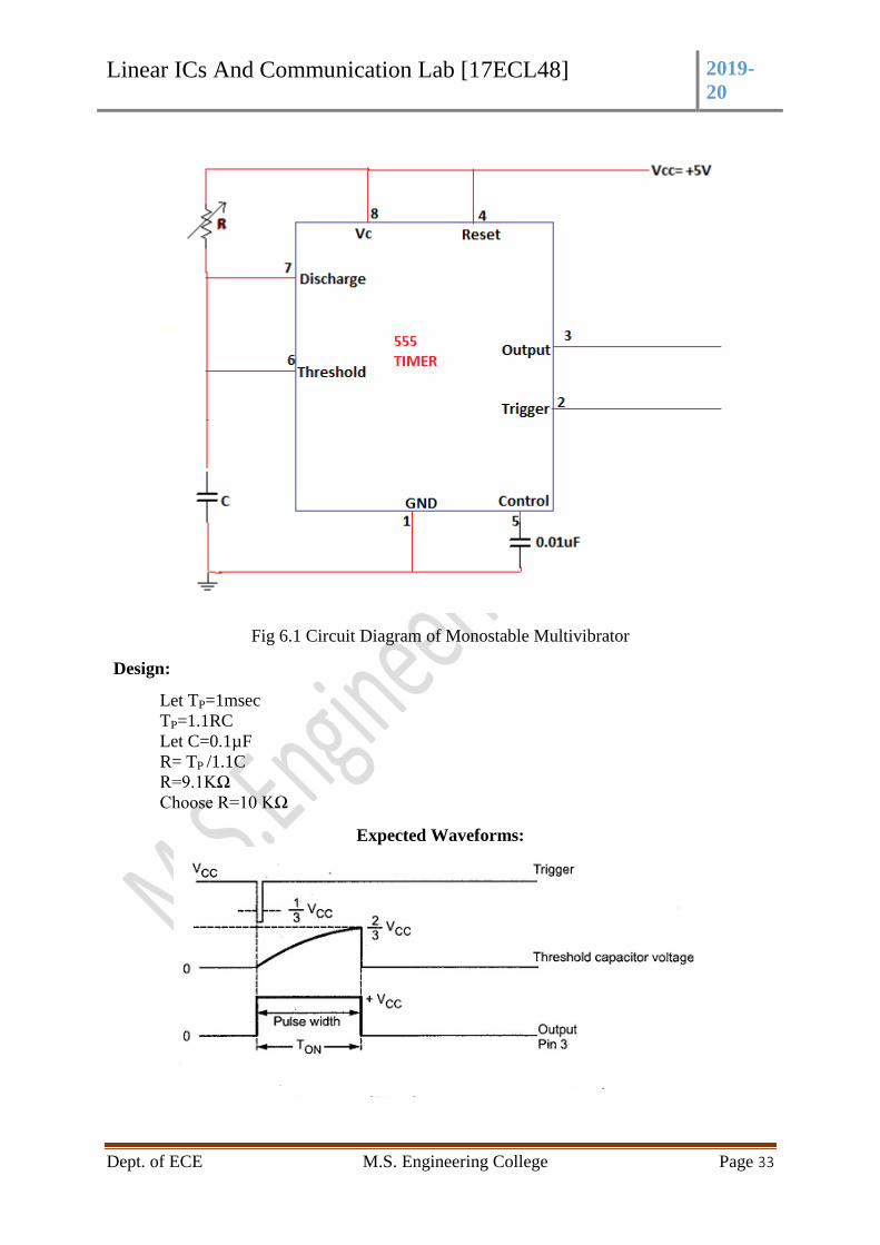
Design:
Let TP=1msec
TP=1.1RC
Let C=0.1µF
R= TP /1.1C
R=9.1KΩ
Choose R=10 KΩ
Expected Waveforms:
Linear ICs And Communication Lab [17ECL48] 2019-
20
Dept. of ECE M.S. Engineering College Page 34
Procedure:
1. Rig up the circuit as shown in the figure.
2. Apply negative triggering input at pin 2 of timer IC.
3. Note the waveform across the capacitor (pin 6 and 1) and output at pin 3 and
measure the peak voltage.
4. Measure the output pulse width and Compare it with the designed value.
Result:
Theoretical Practical
Output pulse width
Astable Multivibrator
Aim: To design and test an astable multivibrator using IC555 timer for a given frequency
and duty cycle.
Components Required: Timer IC 555, Resistor,capacitor 0.1µF,0.01 µF
Theory:
The 555 oscillator now produces a 50% duty cycle as the timing capacitor, C1 is now
charging and discharging through the same resistor, R2 rather than discharging through the
timers discharge pin 7 as before. When the output from the 555 oscillator is HIGH, the
capacitor charges up through R2 and when the output is LOW, it discharges through R2.
Resistor R1 is used to ensure that the capacitor charges up fully to the same value as the
supply voltage.However, as the capacitor charges and discharges through the same resistor,
the above equation for the output frequency of oscillations has to be modified a little to
reflect this circuit change.
Procedure:
Case (i): For given duty cycle > 50% [ 75%]
Circuit Diagram:
Linear ICs And Communication Lab [17ECL48] 2019-
20
Dept. of ECE M.S. Engineering College Page 35
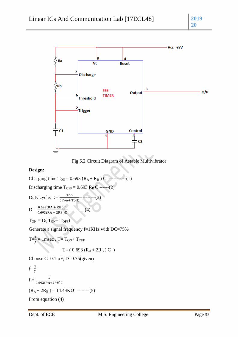
Fig 6.2 Circuit Diagram of Astable Multivibrator
Design:
Charging time TON = 0.693 (RA + RB ) C -----------(1)
Discharging time TOFF = 0.693 RB C ------(2)
Duty cycle, D=
----------(3)
D =
----------(4)
TON = D( TON+ TOFF)
Generate a signal frequency f=1KHz with DC=75%
T=
= 1msec , T= TON+ TOFF
T= ( 0.693 (RA + 2RB ) C )
Choose C=0.1 µF, D=0.75(given)
f =
f =
(RA + 2RB ) = 14.43KΩ --------(5)
From equation (4)
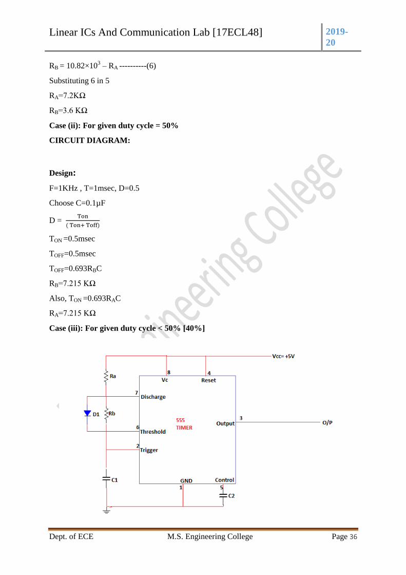
Linear ICs And Communication Lab [17ECL48] 2019-
20
Dept. of ECE M.S. Engineering College Page 36
RB = 10.82×10³ – RA ----------(6)
Substituting 6 in 5
RA=7.2KΩ
RB=3.6 KΩ
Case (ii): For given duty cycle = 50%
CIRCUIT DIAGRAM:
Design:
F=1KHz , T=1msec, D=0.5
Choose C=0.1µF
D =
TON =0.5msec
TOFF=0.5msec
TOFF=0.693RBC
RB=7.215 KΩ
Also, TON =0.693RAC
RA=7.215 KΩ
Case (iii): For given duty cycle < 50% [40%]
Linear ICs And Communication Lab [17ECL48] 2019-
20
Dept. of ECE M.S. Engineering College Page 37
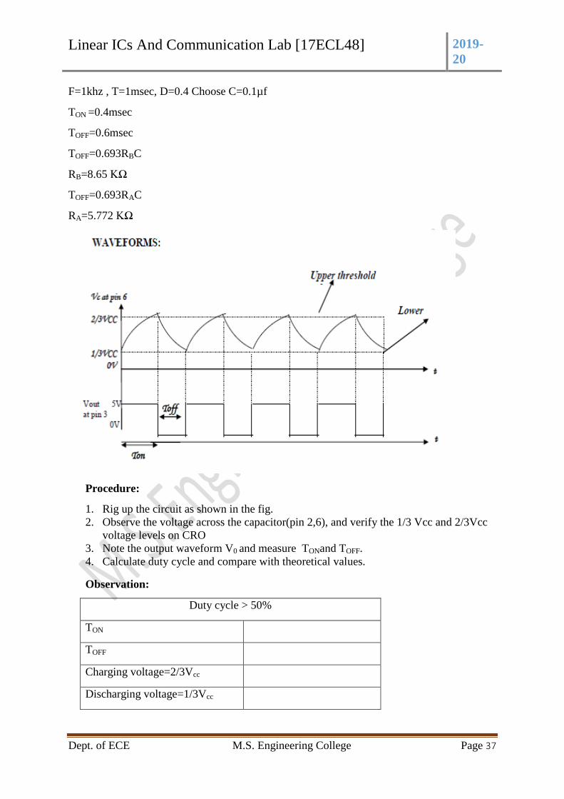
F=1khz , T=1msec, D=0.4 Choose C=0.1µf
TON =0.4msec
TOFF=0.6msec
TOFF=0.693RBC
RB=8.65 KΩ
TOFF=0.693RAC
RA=5.772 KΩ
Procedure:
1. Rig up the circuit as shown in the fig.
2. Observe the voltage across the capacitor(pin 2,6), and verify the 1/3 Vcc and 2/3Vcc
voltage levels on CRO
3. Note the output waveform V0 and measure TONand TOFF.
4. Calculate duty cycle and compare with theoretical values.
Observation:
Duty cycle > 50%
TON
TOFF
Charging voltage=2/3Vcc
Discharging voltage=1/3Vcc
Linear ICs And Communication Lab [17ECL48] 2019-
20
Dept. of ECE M.S. Engineering College Page 38
Duty cycle = 50%
TON
TOFF
Charging voltage=2/3Vcc
Discharging voltage=1/3Vcc
Duty cycle < 50%
TON
TOFF
Charging voltage=2/3Vcc
Discharging voltage=1/3Vcc
Result:
Theoretical Practical
Frequency Duty Cycle Frequency Duty Cycle
Case 1
Case 2
Case 3
Linear ICs And Communication Lab [17ECL48] 2019-
20
Dept. of ECE M.S. Engineering College Page 39
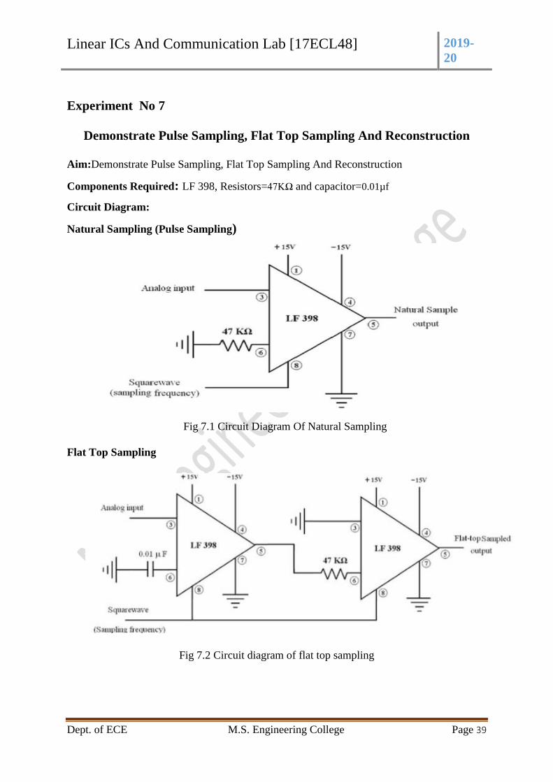
Experiment No 7
Demonstrate Pulse Sampling, Flat Top Sampling And Reconstruction
Aim:Demonstrate Pulse Sampling, Flat Top Sampling And Reconstruction
Components Required: LF 398, Resistors=47KΩ and capacitor=0.01µf
Circuit Diagram:
Natural Sampling (Pulse Sampling)
Fig 7.1 Circuit Diagram Of Natural Sampling
Flat Top Sampling
Fig 7.2 Circuit diagram of flat top sampling
Linear ICs And Communication Lab [17ECL48] 2019-
20
Dept. of ECE M.S. Engineering College Page 40
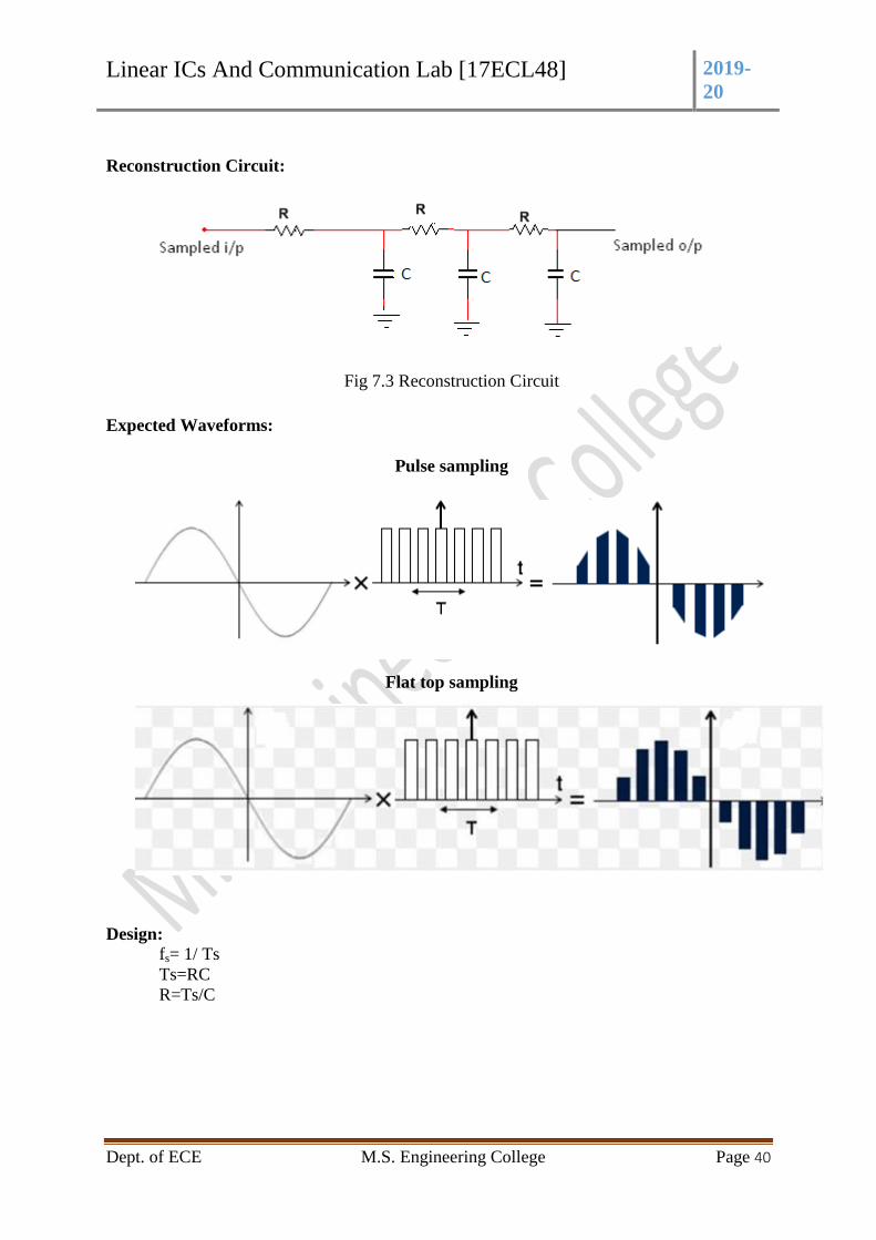
Reconstruction Circuit:
Fig 7.3 Reconstruction Circuit
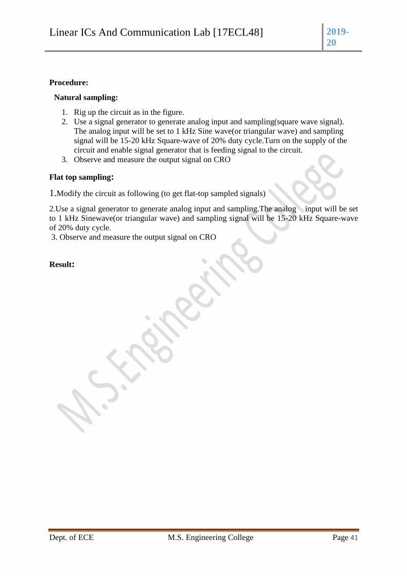
Expected Waveforms:
Pulse sampling
Flat top sampling
Design:
fs= 1/ Ts
Ts=RC
R=Ts/C
Linear ICs And Communication Lab [17ECL48] 2019-
20
Dept. of ECE M.S. Engineering College Page 41
Procedure:
Natural sampling:
1. Rig up the circuit as in the figure.
2. Use a signal generator to generate analog input and sampling(square wave signal).
The analog input will be set to 1 kHz Sine wave(or triangular wave) and sampling
signal will be 15-20 kHz Square-wave of 20% duty cycle.Turn on the supply of the
circuit and enable signal generator that is feeding signal to the circuit.
3. Observe and measure the output signal on CRO
Flat top sampling:
1.Modify the circuit as following (to get flat-top sampled signals)
2.Use a signal generator to generate analog input and sampling.The analog input will be set
to 1 kHz Sinewave(or triangular wave) and sampling signal will be 15-20 kHz Square-wave
of 20% duty cycle.
3. Observe and measure the output signal on CRO
Result:
Linear ICs And Communication Lab [17ECL48] 2019-
20
Dept. of ECE M.S. Engineering College Page 42
Experiment No 8
Amplitude Modulation Using Transistor/Fet (Generation and Detection)
Aim: i. To generate AM signal using collector amplitude modulation for a carrier frequency
of fc=455KHz (Intermediate frequency - IF) and demodulation using envelope detector
Components Required: IFT (Intermediate Frequency Transformer) 455KHZ, Transistor SL100,
Capacitor 0.01µF, Resistor 470KΩ, 120 KΩ , Diode BY127,
Theory : Amplitude modulation is a technique which amplitude of the carrier is changed
according to the modulating signal. The frequency of modulating signal should be less than
carrier. the ratio of voltage of modulating signal to carrier voltage is called modulation index
m and it is expressed as percentage .m ranges from 0 to 1 and if m>1 it is over modulation
and m<m
Design:
Modulation:
µ =
Vm=
Vc=
µ =
where µ= modulation index
Linear ICs And Communication Lab [17ECL48] 2019-
20
Dept. of ECE M.S. Engineering College Page 43
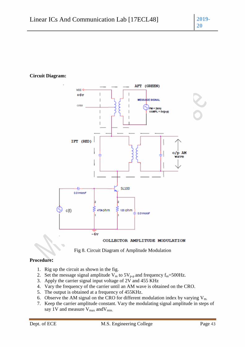
Circuit Diagram:
Fig 8. Circuit Diagram of Amplitude Modulation
Procedure:
1. Rig up the circuit as shown in the fig.
2. Set the message signal amplitude Vm to 5Vp-p and frequency fm=500Hz.
3. Apply the carrier signal input voltage of 2V and 455 KHz
4. Vary the frequency of the carrier until an AM wave is obtained on the CRO.
5. The output is obtained at a frequency of 455KHz.
6. Observe the AM signal on the CRO for different modulation index by varying Vm.
7. Keep the carrier amplitude constant. Vary the modulating signal amplitude in steps of
say 1V and measure Vmax andVmin.
Linear ICs And Communication Lab [17ECL48] 2019-
20
Dept. of ECE M.S. Engineering College Page 44
8. Calculate the modulation index ,tabulate the readings and plot the graph with %μ on
Y- axis and Vm on X-axis.
Note: If necessary check IFT and the tuned frequency using the following steps.
a. Connect the IFT between signal generator and the CRO.
b. Set the input amplitude to 1Vp-p
c. Vary the frequency of signal generator until max output is obtained.
d. The frequency corresponding to max output s the tuned frequency of the IFT.
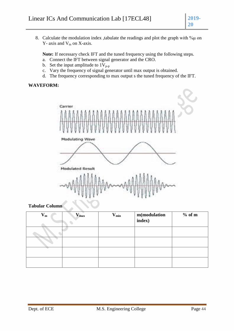
WAVEFORM:
Tabular Column
Vm Vmax Vmin m(modulation
index)
% of m
Linear ICs And Communication Lab [17ECL48] 2019-
20
Dept. of ECE M.S. Engineering College Page 45
Ideal graph
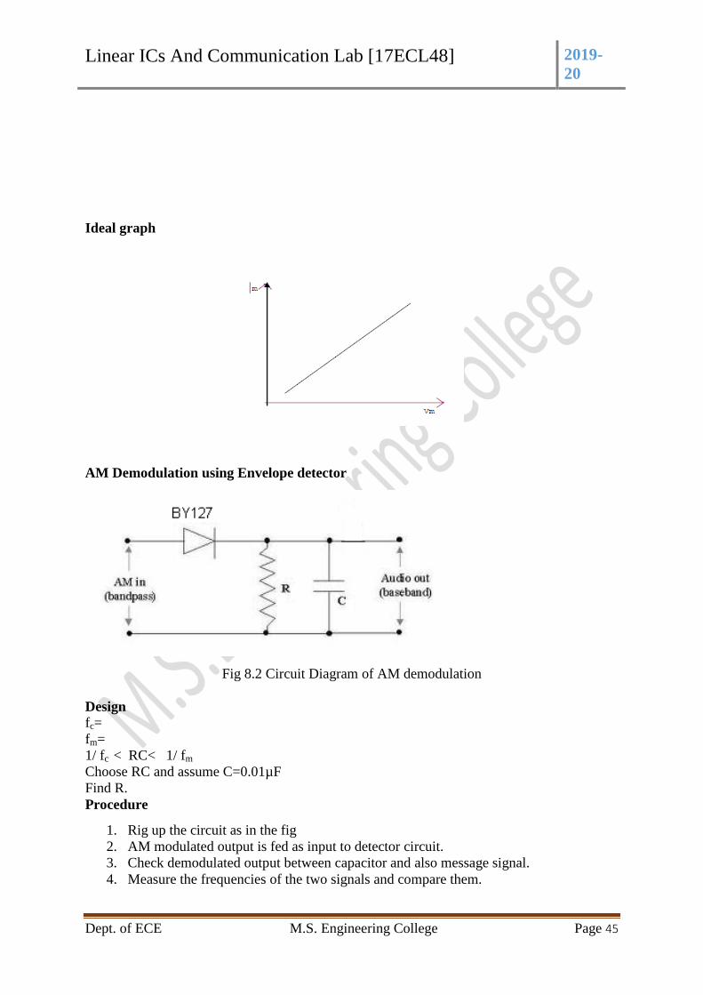
AM Demodulation using Envelope detector
Fig 8.2 Circuit Diagram of AM demodulation
Design
fc=
fm=
1/ fc < RC< 1/ fm
Choose RC and assume C=0.01µF
Find R.
Procedure
1. Rig up the circuit as in the fig
2. AM modulated output is fed as input to detector circuit.
3. Check demodulated output between capacitor and also message signal.
4. Measure the frequencies of the two signals and compare them.
Linear ICs And Communication Lab [17ECL48] 2019-
20
Dept. of ECE M.S. Engineering College Page 46
Result:
The AM Modulated output is observed for the carrier frequency__________ and the
modulation index _____________________with the increase in the message signal.
The message signal frequency _________ and the demodulated signal frequency _____
Linear ICs And Communication Lab [17ECL48] 2019-
20
Dept. of ECE M.S. Engineering College Page 47
Experiment 9
Frequency Modulation Using IC 8038/2206 And Demodulation
Aim: To generate frequency modulated signal using ic 8038 and to find the transmission
bandwidth.
Components required: IC 8038, DCB, resistor, capacitor, bread board
Theory:In frequency modulation the frequency of the carrier is varied according to the
message signal .In frequency modulation amplitude is of the carrier is kept constant while its
frequency is varied .The amount of change in frequency produced by the modulating signal is
known as frequency deviation. maximum frequency deviation occurs maximum amplitude of
modulating signal and minimum frequency deviation occurs at minimum amplitude of
modulating signal.
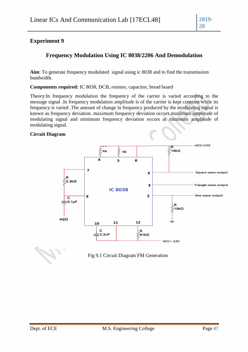
Circuit Diagram
Fig 9.1 Circuit Diagram FM Generation
Linear ICs And Communication Lab [17ECL48] 2019-
20
Dept. of ECE M.S. Engineering College Page 48
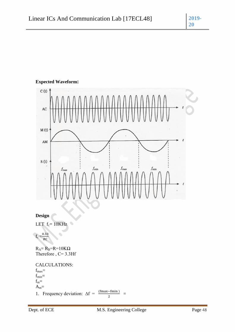
Expected Waveform:
Design
LET fc= 10KHz
fc =
RA= RB=R=10KΩ
Therefore , C= 3.3Ηf
CALCULATIONS:
fmax=
fmin=
fm=
Am=
1. Frequency deviation: ∆f =
=
Linear ICs And Communication Lab [17ECL48] 2019-
20
Dept. of ECE M.S. Engineering College Page 49
2. Modulation index: β =
=
3. Frequency sensitivity = Kf =
=
4. Bandwidth = 2(∆f+ fm) Hz =
PROCEDURE:
1. Rig up the circuit as in the fig.
2. Observe the unmodulated sinusoidal carrier signal at Pin 2 of IC8038 and measure the
amplitude and frequency.
3. Apply modulating signal with amplitude 1V Peak and frequency 500Hz
(approximate).
4. Observe the frequency modulated output at pin2.
5. Note down maximum and minimum frequencies corresponding to two peaks of the
modulating signal.
6. Compute the parameters of the FM signal and tabulate them.
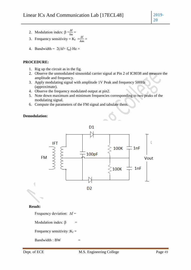
Demodulation:
Result:
Frequency deviation: ∆f =
Modulation index: β =
Frequency sensitivity :Kf =
Bandwidth : BW =
Linear ICs And Communication Lab [17ECL48] 2019-
20
Dept. of ECE M.S. Engineering College Page 50
Demodulated frequency =
Experiment No 10
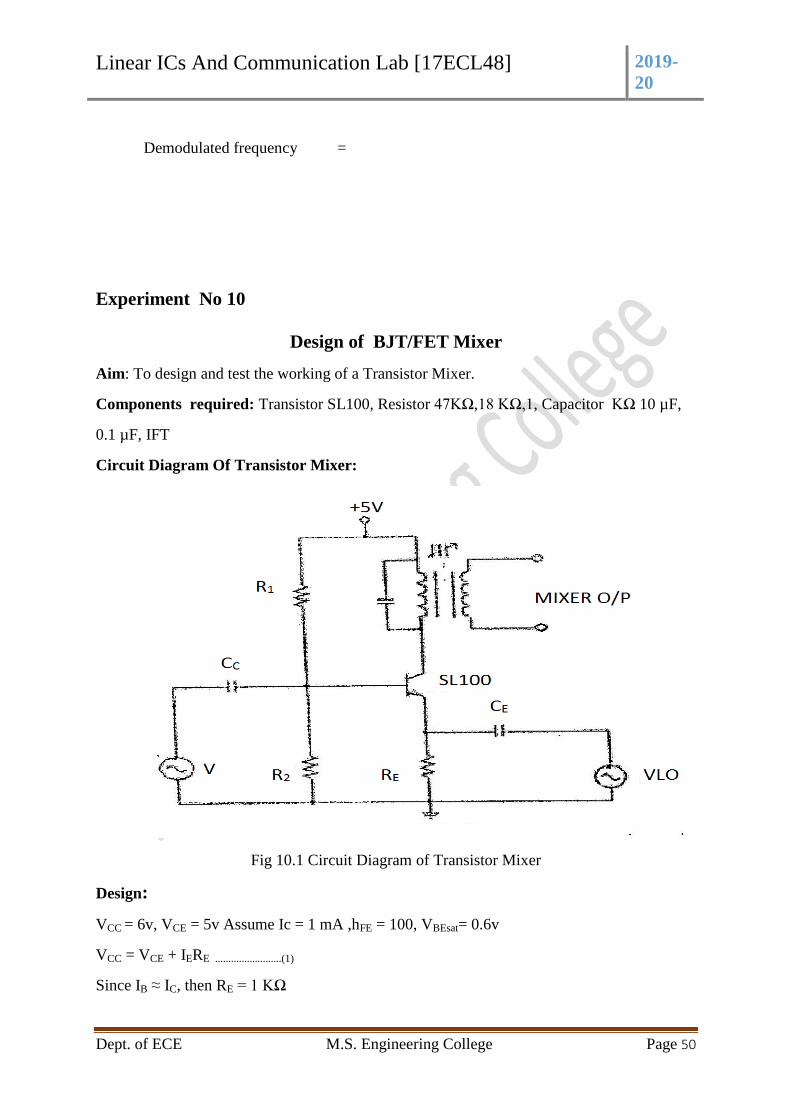
Design of BJT/FET Mixer
Aim: To design and test the working of a Transistor Mixer.
Components required: Transistor SL100, Resistor 47KΩ,18 KΩ,1, Capacitor KΩ 10 µF,
0.1 µF, IFT
Circuit Diagram Of Transistor Mixer:
Fig 10.1 Circuit Diagram of Transistor Mixer
Design:
VCC = 6v, VCE = 5v Assume Ic = 1 mA ,hFE = 100, VBEsat= 0.6v
VCC = VCE + IERE .........................(1)
Since IB ≈ IC, then RE = 1 KΩ
Linear ICs And Communication Lab [17ECL48] 2019-
20
Dept. of ECE M.S. Engineering College Page 51
Vb = IBRB + VBEsat + IERE
Where Vb = VCC *
, Rb =R1 *
From Eq(1) it can be found that R1 =2.5R2 , Choose R2 = 18KΩ,
then R1 = 45KΩ. Select R1 = 47KΩ, R2 = 18KΩ, RE = 1KΩ, CC = 0.1 µF,
CE = 10 µF
Procedure:
1. Connections are made as shown in the circuit diagram.
2. Keeping the amplitude of the local Oscillator in minimum position, find the tuned
frequency of IFT (fIFT) by varying the carrier frequency (fS) of the input AM signal.
Down Conversion:
1. Adjust the carrier frequency of the AM signal more than the tuned frequency of IFT,
now adjusting the local oscillator frequency ( fLO = fS + fIFT).(NOTE: Local oscillator
amplitude not equal to zero),observe the AM output signal with carrier frequency at
fIFT.
2. Observe the AM input signal and AM signal at the IFT output and measure carrier
Frequencies fcin and fcout.
Up Conversion:
1. Adjust the carrier frequency of the AM signal less than the tuned frequency of IFT,
now adjusting the local oscillator frequency ( fLO = fS + fIFT).(NOTE: Local oscillator
amplitude not equal to zero),observe the AM output signal with carrier frequency at
fIFT.
2. Observe the AM input signal and AM signal at the IFT output and measure carrier
Frequencies fcin and fcout.
Linear ICs And Communication Lab [17ECL48] 2019-
20
Dept. of ECE M.S. Engineering College Page 52
Experiment No 11
DSBSC Generation Using Balance Modulator IC 1496
Aim: To generate AM- Double sideband Supressed carrier signal (DSB-SC) signal.
Components required: IC 1496, Resistors, capacitors as per design, Signal generator, CRO
bread board.
Circuit Diagram
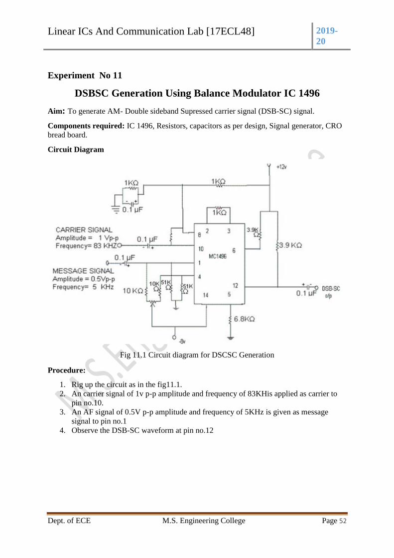
Fig 11.1 Circuit diagram for DSCSC Generation
Procedure:
1. Rig up the circuit as in the fig11.1.
2. An carrier signal of 1v p-p amplitude and frequency of 83KHis applied as carrier to
pin no.10.
3. An AF signal of 0.5V p-p amplitude and frequency of 5KHz is given as message
signal to pin no.1
4. Observe the DSB-SC waveform at pin no.12
Linear ICs And Communication Lab [17ECL48] 2019-
20
Dept. of ECE M.S. Engineering College Page 53
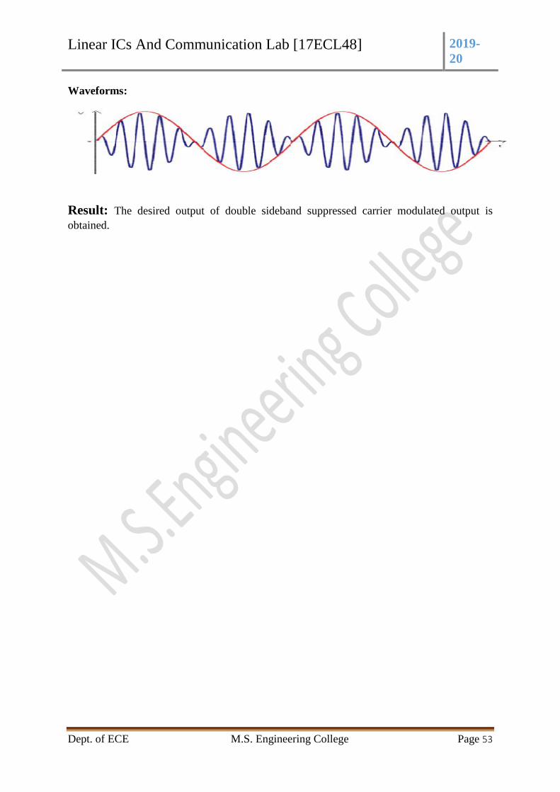
Waveforms:
Result: The desired output of double sideband suppressed carrier modulated output is
obtained.
Linear ICs And Communication Lab [17ECL48] 2019-
20
Dept. of ECE M.S. Engineering College Page 54
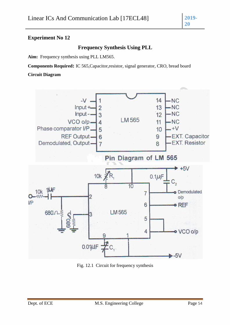
Experiment No 12
Frequency Synthesis Using PLL
Aim: Frequency synthesis using PLL LM565.
Components Required: IC 565,Capacitor,resistor, signal generator, CRO, bread board
Circuit Diagram
Fig. 12.1 Circuit for frequency synthesis
Linear ICs And Communication Lab [17ECL48] 2019-
20
Dept. of ECE M.S. Engineering College Page 55
Procedure:
1.Connections are made as shown in the figure
2.By varying the frequency in different steps observe that at one frequency the waveform will
be phase locked.
3.Change RC component to shift VCO center frequency and see how lock range of the input
varies.
4.Now compare the theoretical and practical values using the formul
Where F0= free running frequency
C1=External Capacitor
R1= External Resistor
FC=
Whrere FC= Capture Range
C2= Filter capacitor
=
in Hz
Where = Lock range
Result:PLL is studied and the practical values of capture range and lock range are
compared with theoretical values.
Linear ICs And Communication Lab [17ECL48] 2019-
20
Dept. of ECE M.S. Engineering College Page 56
Related Documents
![Low-Power Linear Active Thermistor ICs - start [EIF Wiki]](https://static.cupdf.com/doc/110x72/615815ab7f4d1970ef044ab5/low-power-linear-active-thermistor-ics-start-eif-wiki.jpg)