EUROPEAN ORGANIZATION FOR NUCLEAR RESEARCH CERN ECP/ 96-03 5 January 1996 LHC1: A semiconductor pixel detector readout chip with internal, tunable delay providing a binary pattern of selected events Erik H.M. Heijne 1 , F. Antinori 1 , D. Barberis 4 , K.H. Becks 14 , H. Beker 1 , W. Beusch 1 , P. Burger 15 , M. Campbell 1 , E. Cantatore 1,3 , M.G Catanesi 3 , E. Chesi 1 , G. Darbo 4 , S. D'Auria 7,10 , C. DaVia' 1,10 , D. Di Bari 3 , S. Di Liberto 6 , T. Gys 1 , G. Humpston 16 , A. Jacholkowski 1 , J.J. Jæger 8 , J. Jakubek 11 , P. Jarron 1 , W. Klempt 1 , F. Krummenacher 17 , K. Knudson 1 , J. Kubasta 11 , J.C. Lassalle 1 , R. Leitner 11 , F. Lemeilleur 1 , V. Lenti 3 , M. Letheren 1 , B. Lisowski 9 , L. Lopez 1 , D. Loukas 2 , M. Luptak 12 , P. Martinengo 1 , G. Meddeler 1 , F. Meddi 6 , P. Middelkamp 1,14 , M. Morando 5 , P. Morettini 4 , A. Munns 16 , P. Musico 4 , F. Pellegrini 5 , F. Pengg 1 , S. Pospisil 11 , E. Quercigh 1 , J. Ridky 11 , L. Rossi 4 , K. Safarik 1 , L. Scharfetter 1 , G. Segato 5 , S. Simone 3 , K. Smith 10 , W. Snoeys 1 , C. Sobczynski 13 , J. Stastny 11 and V. Vrba 11 CERN 1 , Techn. University Athens 2 , INFN and University of Bari 3 , Genova 4 , Padova 5 , Roma 6 , Udine 7 , Collège de France 8 , University Dortmund 9 , Glasgow University 10 , Group Praha 11 , Inst. of Exp. Physics Kosice 12 , Warsaw University 13 , University GHS Wuppertal 14 , Canberra Semiconductor NV 15 , GEC Marconi (Caswell) 16 and Smart Silicon Systems SA 17 . representing collaborators from CERN Detector R&D Collaboration RD19 and Experiment WA97. Abstract The Omega3/LHC1 pixel detector readout chip comprises a matrix of 128 x 16 readout cells of 50 μm x 500 μm and peripheral functions with 4 distinct modes of initialization and operation, together more than 800 000 transistors. Each cell contains a complete chain of amplifier, discriminator with adjustable threshold and fast-OR output, a globally adjustable delay with local fine-tuning, coincidence logic and memory. Every cell can be individually addressed for electrical test and masking. First results have been obtained from electrical tests of a chip without detector as well as from source measurements. The electronic noise without detector is ~ 100 e - rms. The lowest threshold setting is close to 2000 e - and non-uniformity has been measured to be better than 450 e - rms at 5 000 e - threshold. A timewalk of < 10 ns and a precision of < 6 ns rms on a delay of 2 μs have been measured. The results may be improved by further optimization.

Welcome message from author
This document is posted to help you gain knowledge. Please leave a comment to let me know what you think about it! Share it to your friends and learn new things together.
Transcript
EUROPEAN ORGANIZATION FOR NUCLEAR RESEARCH
CERN ECP/ 96-035 January 1996
LHC1: A semiconductor pixel detector readout chip with internal,tunable delay providing a binary pattern of selected events
Erik H.M. Heijne1, F. Antinori1, D. Barberis4, K.H. Becks14, H. Beker1, W. Beusch1, P. Burger15,M. Campbell1, E. Cantatore1,3, M.G Catanesi3, E. Chesi1, G. Darbo4, S. D'Auria7,10 , C. DaVia'1,10,D. Di Bari3, S. Di Liberto6, T. Gys1, G. Humpston16, A. Jacholkowski1, J.J. Jæger8, J. Jakubek11,
P. Jarron1, W. Klempt1, F. Krummenacher17, K. Knudson1, J. Kubasta11, J.C. Lassalle1, R. Leitner11,F. Lemeilleur1, V. Lenti3, M. Letheren1, B. Lisowski9, L. Lopez1, D. Loukas2, M. Luptak12,
P. Martinengo1, G. Meddeler1, F. Meddi6, P. Middelkamp1,14, M. Morando5, P. Morettini4, A. Munns16,P. Musico4, F. Pellegrini5, F. Pengg1, S. Pospisil11, E. Quercigh1, J. Ridky11, L. Rossi4, K. Safarik1,L. Scharfetter1, G. Segato5, S. Simone3, K. Smith10, W. Snoeys1, C. Sobczynski13, J. Stastny11 and
V. Vrba11
CERN1, Techn. University Athens2, INFN and University of Bari3, Genova4, Padova5, Roma6, Udine7, Collège de France8,
University Dortmund9 , Glasgow University10, Group Praha11, Inst. of Exp. Physics Kosice12, Warsaw University13 ,
University GHS Wuppertal14, Canberra Semiconductor NV15, GEC Marconi (Caswell)16 and Smart Silicon Systems SA17.
representing collaborators from CERN Detector R&D Collaboration RD19 and Experiment WA97.
Abstract
The Omega3/LHC1 pixel detector readout chip comprises a matrix of 128 x 16 readout cells of
50 µm x 500 µm and peripheral functions with 4 distinct modes of initialization and operation, together
more than 800 000 transistors. Each cell contains a complete chain of amplifier, discriminator with
adjustable threshold and fast-OR output, a globally adjustable delay with local fine-tuning, coincidence
logic and memory. Every cell can be individually addressed for electrical test and masking. First results
have been obtained from electrical tests of a chip without detector as well as from source measurements.
The electronic noise without detector is ~ 100 e- rms. The lowest threshold setting is close to 2000 e- and
non-uniformity has been measured to be better than 450 e- rms at 5 000 e- threshold. A timewalk of
< 10 ns and a precision of < 6 ns rms on a delay of 2 µs have been measured. The results may be improved
by further optimization.

Hiroshima Symposium 1995, submitted to Nuclear Instruments and Methods A.
1. Introduction
Pixel detectors are gradually gaining credibility as reliable devices for ~10 µm precision particle
detection in high multiplicity, high rate particle physics experiments. At present a 500 000 pixel cell
telescope using the Omega2 readout chip bump-bonded to a silicon matrix and comprising 7 planes of
~ 30 cm2 each is taking data at CERN in the WA97 heavy ion experiment [1-5]. This operation, successful
in most respects, provides lessons for improvements, in particular concerning homogeneity, production
yield and testability of the chips. Here we report on the first, to some extent still preliminary results
obtained with the improved Omega3/LHC1 chip and hybrid detector assemblies, designed to satisfy the
requirements of WA97 and at the same time to explore ways towards future LHC vertex detector
requirements.
The choice of binary operation as opposed to full analog readout is adequate for most tracking
purposes. It helps to reduce power needs for signal transmission and tends to reduce cell size. The
asynchronous operation of the front-end amplifier, latched comparator and tunable delay line reduces the
risk of feedthrough of clock signals into the highly sensitive input of the front-end. In this architecture pixel
hit data generated after ~150 ns is stored locally in the delay line and read out for selected events only. This
provides low power consumption and minimal traffic on the chip busses. In contradiction with this
philosophy, a fast-OR signal is transmitted by every hit to the bottom of the column, using 0-10 µA logic, in
order to allow alternative schemes for trigger generation and resolving eventual timing ambiguities. To
prevent parasitic signal feedthrough the second level metal layer is used for shielding.
The chip covers a sensitive area of 8 mm x 6.35 mm, just over 0.5 cm2 , with a matrix of 16 x 127
readout cells, and has a total area of 0.8 cm2. It has been manufactured in the 1 µm SACMOS process from
FASELEC [6], selected because of high component density, equivalent to a 0.6 µm standard CMOS
process. We intend to mount 6 chips together onto one detector, called 'ladder', so good die must be
identified before assembly and full testing on wafer is foreseen.
The non-uniformity from cell-to-cell of threshold and delay on the previous chip [7,8] was not
satisfactory for future LHC applications. The discriminator and delay were redesigned. Timewalk was
minimized for good timing resolution and dead time was reduced to avoid loss of hit data. In addition to
the cell-to-cell uniformity also the insufficient chip-to-chip uniformity in the WA97 telescope showed the
need for individual adjustment of bias supplies per chip. A control chip, the COOP, which also contains an
event buffer and zero suppression has been designed [9] for this purpose. In sect. 2 the design of the pixel
cell is explained in some detail. The matrix, peripheral logic and modes of operation are discussed in sect.
3. In sect. 4 finally measurement results are presented.
2. Description of the pixel cell
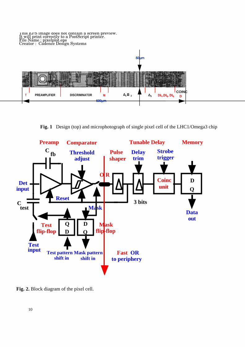
Figure 1 shows layout and photograph of one matrix pixel element, which contains about 400
transistors in an area of 500 µm length by 50 µm width. Fig. 2 shows the corresponding block diagram.
The pixel readout chain contains from left to right the successive functions: flip-flop for connection of
analog test signal (length 25 µm), bump-pad (octogonal in metal 1 and 2 with 22 µm diameter), preamplifier

4
with leakage current compensation, asynchronous comparator with externally adjustable threshold and fast-
OR output (preamp and comparator ~ 250 µm), the masking flip-flop (25 µm), a globally adjustable delay
(100 µm) with local 3-bit fine-tuning (100 µm), coincidence logic, memory cell (25 µm) and bus lines.
The input of each pixel is connected by a solder bump to a corresponding matrix element on the
semiconductor detector. Fig. 3 shows a picture of such bumps before connection. The bumps connect to
silicon diode detector elements that are also 50 µm x 500 µm. On the photograph in fig. 4 of a part of the
detector chip one may just distinguish the circular contact opening on the right end of each cell. Dummy
cells, at the bottom, connected by thin lines to a guard ring, surround the matrix of active cells. The guard
ring is connected to a separate ground on the readout chip. The lowest pixel cell in fig. 4 is connected to the
current sensing circuit on the readout chip and provides a compensation current of up to 10 nA for each of
the the 127 active cells in the column, i.e. up to 40 µA cm-2.
The charge preamplifier is based on a folded cascode circuit similar to that in the Omega2 chip and is
designed to consume 19 µW. The feedback capacitance Cfb is about 3.5 fF. The feedback resistance is
non-linear to limit the swing for high input signals. Following extraction of parasitics and resimulation a
source follower was added at the output to improve speed. The signal risetime is designed ~80 ns. An
additional reset has been provided to force a fast return to zero to decrease the dead-time of the cell after a
large signal.
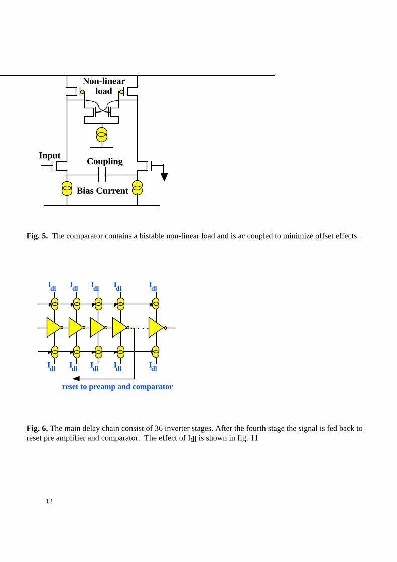
The comparator (fig. 5) is structurally the same as in Omega2 and is designed to operate at low power,
15 µW. The current in the bistable nonlinear load determines the threshold and can be varied externally via
a common bias adjustment. In the state after reset this current runs in one of the two branches of the non-
linear load. A large enough signal will cause the bistable load to change state switching the current to the
other side. This change is detected by a fast sensing circuit and latched. Attention was paid to threshold
uniformity by symmetric layout of the two branches and the non-linear load and by proper dimensioning of
transistors. We used matching data provided by Faselec AG on the SACMOS2 process, extrapolated to the
SACMOS1 process.. A tradeoff with timewalk had to be made as a large load transistor improves matching
but slows down response by increased capacitance. The reset (together with preamp reset) can be external
or from the feedback from the delay chain. The comparator provides a fast-OR and it can be masked, i.e.
inhibited to operate if the preamp or the comparator prove to be too noisy or defective. The fast-OR outputs
of all cells in a column are connected together in a wired-OR configuration.
The delay chain (fig. 6) is based on current-deprived inverters: 36 stages now instead of 3 in Omega2.
This together with the feedback after 4 stages to reset the front-end allows several hit pulses to propagate
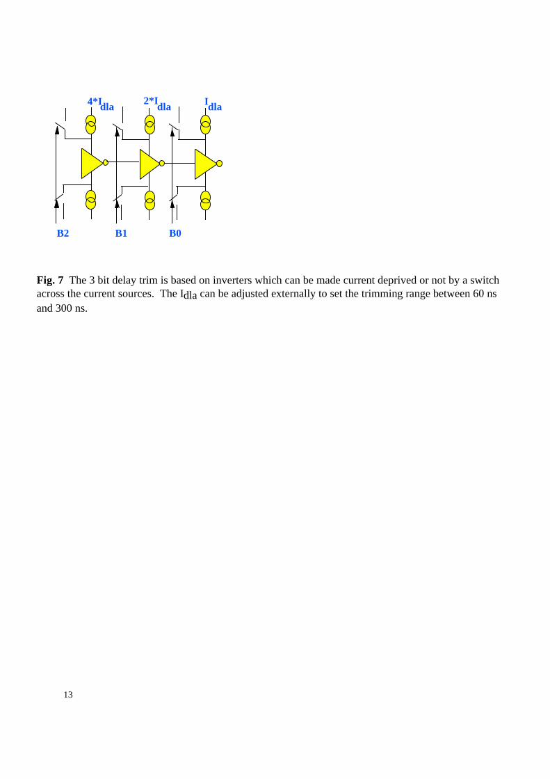
consecutively in the delay line and should decrease dead-time to below ~250 ns. As distinctive feature a 3-
bit digitally controlled delay tuning has been added. This trimming delay contains 3 more inverter stages
which can be made current-deprived or not by a switch across the current source, as indicated in fig. 7. A
fourth inverter is used to restore a proper edge of the signal before it is used in the subsequent coincidence
logic. The coincidence logic will write a one into the data flip-flop if during the externally provided strobe
5
a rising edge at the end of the delay line is detected. The data flip-flops of all pixels in one column are
configured as a shift-register during data readout.
3. Peripheral functions, modes of operation
As mentioned already in the introduction the readout chip LHC1/Omega3 contains a one-sided
peripheral region and a matrix of readout cells of 16 columns and 128 rows: 127 active rows, 1 test row at
the top, and a row of current sensing cells at the bottom which are connected to dummy sensor cells on the
detector, one for each column. A photograph of the complete chip is shown in fig. 8. The chip size is
8.72 mm x 9.12 mm of which 63% is sensitive area. All 16 cells of the test row are permanently connected
to the analog test input, contrary to the active pixels, which are optionally connected by digital control of
the test flip-flop. This allows to write various test patterns, but it is undesirable to address all cells in the
matrix at the same time because there may be excessive load on the power supplies.
The peripheral functions are naturally organized according to the column structure as is clear from
fig. 8. Because of the need to butt together several chips on a ladder, only one side, the'bottom', is used for
these peripheral functions. Biases are regenerated here for each column and logic signals are buffered. The
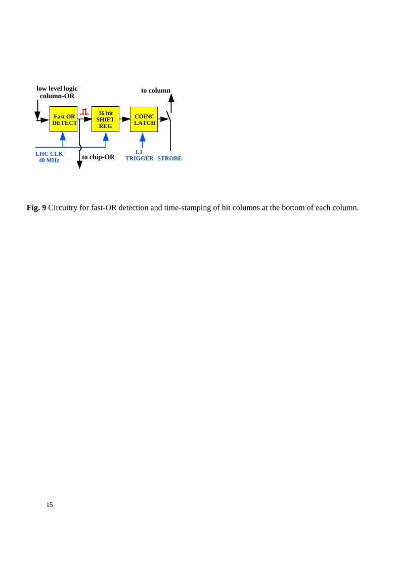
wired fast-OR in the column is detected and buffered. On the one hand this signal is used to produce a
chip-wide OR, sent off-chip for possible trigger purposes, and which allows to self-generate a strobe for the
event data. On the other hand the OR signal of a column is used on-chip as time-stamp to resolve possible
ambiguities. If this circuit (fig. 9) is enabled and a hit in the column is detected via a fast-OR, a one is
written into a 40 MHz shift register, which corresponds to the LHC bunch-crossing clock frequency. If the
length of the shift register is chosen appropriately, taking into account the trigger latency and delay between
hit and fast-OR, the output of the shift register can be used as an enable signal for the eventual strobe. The
strobe then would not be applied to the pixels if in that column no hit was present in the time slot of interest.
This would allow to use a strobe wider than 25 ns in case the delay within each pixel is not sufficiently
accurate across the chip. At present the depth of the shift register has been limited to 16, it should be
adjusted to 80 or 120 for expected trigger latency times in ATLAS resp. CMS.
The periphery of the chip also contains bidirectional tristate output buffers to read data and to write
and read contents of the various registers. Control logic defines the four distinct operation modes selectable
via external control lines.
Mode 0 (Omega operation) This 'normal' mode covers also the actual operation in Omega2.
During data taking the strobe is connected to all pixels. If a hit of sufficient amplitude has been sensed in
one of the pixels within the strobe time, the data flip-flop of that pixel will be set. Readout requires 128
clock pulses to shift out the rows of data after a strobe. One may apply the clock to certain columns only
and keep others in data collection mode which allows to determine possible cross-talk during readout.
Mode 1 (LHC operation) Instead of applying the strobe to each column directly, it is enabled by a
signal generated on-chip by the fast-OR of the column as described earlier. This allows a wider strobe to be
6
used while keeping timing ambiguities rare. This facility has been included to cope with LHC timing needs
in case of unsatisfactory uniformity of the delays within each pixel.
Mode 2 (Initialize Delay adjust register) and 3 (initialize Test and Mask registers) These initialisation
('slow control') modes allow to read and write the contents of the delay adjust register (3 bits per pixel), and
the test and mask registers (twice one bit per pixel).
In both Omega (0) and LHC (1) mode, the delay adjust and external fast-OR output can be enabled or
disabled.
4. Timing and threshold measurements
The threshold and timing uniformity are critical parameters of any pixel readout system for particle
physics experiments. In recent beam measurements using the Omega2 pixel chip bump-bonded to a 300 µm
thick Si detector [5] we have demonstrated that 100% detection efficiency for high enery particles can be
obtained if the pixel threshold is set at ~ 9 000 e-.
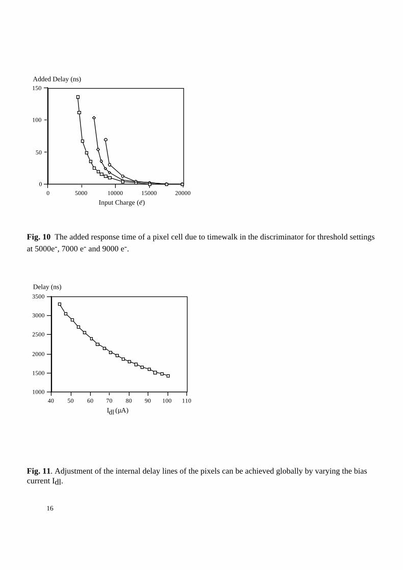
Timewalk
In fig. 10 the timewalk in one pixel cell in the LHC1 chip is shown. This measurement was made on
one of the test pixels at the top of the matrix using electrical stimulation. A timewalk of better than 10 ns
can be observed for input signals above ~ 9 000 e- for a pixel
threshold at or below ~ 5 000 e-. It is to be noted that the optimal biasing of the circuit for lowest
possible threshold was not yet achieved for the data reported in the figs. 10 - 15. While a threshold
~2000 e- has been used already on the full matrix, there are indications that an even lower value is possible
but some digital interference may prevent operation of all cells at such low thresholds.
Adjustable delay
While discussing the internal pixel delay lines it was mentioned that these can be adjusted globally.Fig. 11 shows the dependence of the average pixel delay on the bias current Idl. This delay can be adjusted
between 1.5 µs and 3 µs. The expected latency time for the level-1 trigger in ATLAS is ~2 µs while in
CMS it is 3 µs. The uniformity of this delay determines the minimum strobe duration needed to detect allhits belonging to one event. We expected random effects in CMOS transistor threshold voltages (Vt) to
dominate the fluctuations in delay. The critical components were dimensioned to be as large as possible
within the limited area available and 36 invertor stages were implemented in the delay chain to minimize
these fluctuations. However, as can be observed from fig. 12(a), the measured delay fluctuation across one
chip is rather systematic from top to bottom of the chip. A similar, but less pronounced behaviour was
observed from left-to-right as well. This systematic variation seems to correlate with a rather pronouncedVt gradient across the wafer. The delay variation for the first evaluated chips is a factor of 2 greater than
assumed in the design.
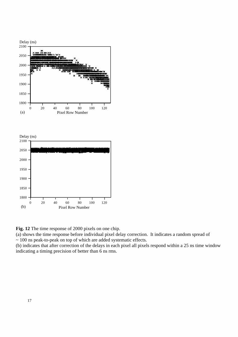
Individual pixel tuning
In order to obtain the timing precision needed in LHC experiments a delay tuning is provided for each
pixel individually. It is controlled by the content of a 3-bit register in the pixel which can be addressed
externally. The delay correction is done in 2 steps. The range of delay variation is determined and the
7
delay adjust current, Idla, is adapted to cover this range. Then the appropriate 3-bit code is written into
every pixel to implement the individual delay correction. In fig. 12(b) the corrected response time of the
pixels on one chip is shown. All pixels respond within a 25 ns window indicating a precision of better than
6 ns rms. This measurement is executed with a uniform, electrical signal. For particle signals timewalk has
to be included to obtain actual timing.
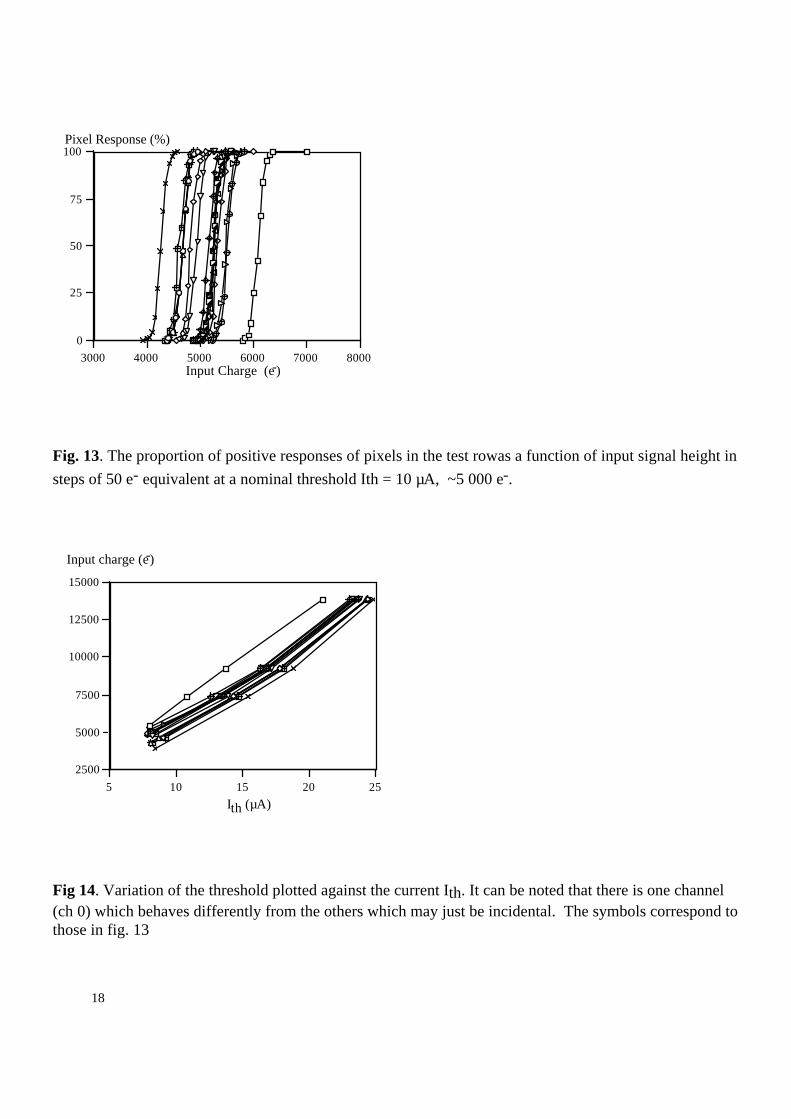
Threshold measurementsIt was explained how the threshold can be varied as a function of the current Ith.which biases the
bistable non-linear load of the discriminator. However, there is a certain threshold spread between pixels.
In order to quantify this spread and to estimate the noise in the front-end the electrical input signal was
varied and the number of positive responses per trigger (expressed as a %) was measured. The curves
obtained for the test row are shown in fig. 13. Taking the 50% point in the curves as threshold we can
determine an estimate for the threshold variation, be it with low statistics. At this threshold the variation is
450 e- rms. The difference in input signal between 2 % reponse and 98 % response corresponds to 4σ of
the noise distribution. This yields an estimated electronic noise of ~100 e- rms for the test row which is notconnected to a sensor element. By increasing the external bias current Ith from 5 µA upwards the thresholds
are moving nearly linearly up to ~ 15 000 e- as illustrated in fig. 14. It has been noticed that there is a
systematic top-down gradient and on some chips also a slight left-right gradient in the effective threshold
value. These systematic gradients influence in particular the timewalk characteristics and improvements in
the performance can be expected if the cause for the gradients can be eliminated.
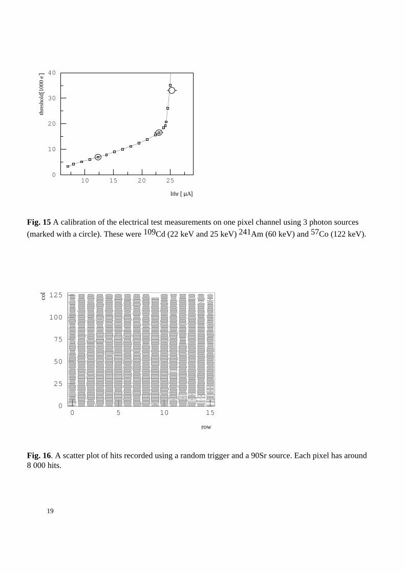
Calibration of threshold using radioactive sources
In order to calibrate the electrical measurements of threshold and uniformity, a fully assembled
readout chip with detector was exposed to radioactive sources with well-defined photon emission lines.These were 109Cd (22 keV and 25 keV), 241Am (60 keV) and 57Co (122 keV). The threshold current, Ith, of
the chips was varied in small steps and each time the number of photons counted for a fixed number of
trigger strobes was recorded for every pixel. When the threshold increases beyond the characteristic photon
energy the count rate falls to zero. This allows to determine the threshold current required to obtain a
particular threshold on every pixel. As shown in fig. 15 the 3 calibration points could be superimposed to
an electrical threshold scan of the same chip. This provides a threshold calibration in absolute energy and in
equivalent incident e-. This allows to determine independently the exact value of the injection capacitance
and in this case it was found to be equal to the expected one. In fig. 15 the threshold is again shown to vary
linearly between 3 000 e- and 15 000 e-. Beyond that the discrininator is still functional, but the thresholdsensitivity to Ith increases strongly. Using this calibration curve and the data for the 241Am source the
threshold variation across the whole chip could be estimated. A threshold distribution with a variance of
~ 700 e- rms for a seting at 16 500 e- was obtained. Further threshold measurements are in progress.
Overall detector response
Various measurements were performed with the first detector assemblies using sources. The fast-OR
was used in order to increase efficiency of data taking with the randomly incident electrons. The fast-OR
8
signal with its low voltage swing current logic did not generate any noticeable feedthrough into the sensitive
pixel inputs. Fig. 16 shows the scatter plot resulting in a uniform distribution of hits from an irradiation
using electrons from a 90Sr source. 10 million events were accumulated with a random trigger.
5. Conclusion
The Omega3/LHC1 pixel readout chip has been bump-bonded to a 300 µm thick Si detector and
functionality of most features has been demonstrated. The noise without detector (100 e- rms) has been
estimated by electrical measurements. Threshold is linearly adjustable between ~2 000 e- and 15 000 e- and
threshold non-uniformity has been measured electrically (~450 e- rms @ 5000 e- threshold) and using
radioactive sources (~700 e- rms @ 16 500 e- threshold). Timewalk (< 10 ns) and delay precision
(< 6 ns rms) have been measured electrically and demonstrate the suitability of the architecture for future
LHC applications. The fast-OR circuit works and has been used in radioactive source measurements. Some
more advanced features of the chip remain to be tested, in particular the synergy with the COOP control
chip, and statistics on various characteristic parameters should be obtained. Practical application of the
detectors is foreseen in a new, 8 plane telescope for the WA97 heavy ion experiment in the Omega
spectrometer at CERN.
References
[1] E.H.M. Heijne, F. Antinori, D. Barberis, H. Beker, W. Beusch, P. Burger, M. Campbell, E. Cantatore, E. Catanesi, E. Chesi,G. Darbo, S. D'Auria, C. DaVia', D. Di Bari, S. Di Liberto, D. Elia, T. Gys, H. Helstrup, J. Heuser, A. Jacholkowski, P. Jarron,W. Klempt, I. Kralik, F. Krummenacher, J.C. Lasalle, R. Leitner, F. Lemeilleur, V. Lenti, M. Lokajicek, L. Lopez, M. Luptak,G. Maggi, P. Martinengo, F. Meddi, A. Menetrey, P. Middelkamp, M. Morando, A. Munns, P. Musico, F. Pellegrini, S. Pospisil,E. Quercigh, J. Ridky, L. Rossi, K. Safarik, G. Saladino, G. Segato, S. Simone, W. Snoeys, G. Stefanini and V. Vrba
Construction and characterization of a 117 cm2 siliconpixel detector IEEE Trans. Nucl. Sci. NS-42 (1995) 413.
[2] F. Antinori, D. Barberis, H. Beker, W. Beusch, M. Campbell, E. Cantatore, M.G. Catanesi, E. Chesi, G. Darbo, D. Di Bari,S. Di Liberto, D. Elia, E.H.M. Heijne, H. Helstrup, A. Jacholkowski, W. Klempt, K. Knudson, I. Kralik, J.C. Lassalle, V. Lenti, L.Lopez, M. Luptak, P. Martinengo, F. Meddi, P. Middelkamp, M. Morando, F. Pellegrini, E. Quercigh, L. Rossi, K. Safarik, G. Segatoand S. Simone Developmentof silicon pixels for strangeness detection in nucleus-nucleus collisions proceedingsof Quark Matter '95 Monterey, CA, USA , AIP Conf. Proc. 340, ed. J. Rafelski.
[3] A. Jacholkowski et al. First results from experiment WA97 to be publ. in proc. Moriand '95, 19-25 March, Les Arcs, France.
[4] E.H.M. Heijne, F. Antinori, R. Arnold, D. Barberis, H. Beker, W. Beusch, P. Burger, M. Campbell, E. Chesi, G. Darbo, C. DaVia', D.Di Bari, S. Di Liberto, D. Elia, C.C. Enz, M. Glaser, J.L. Guyonnet, T. Gys, H. Helstrup, J. Heuser, A. Jacholkowski, P. Jarron,S. Kersten, F. Krummenacher, R. Leitner, F. Lemeilleur, V. Lenti, M. Letheren, M. Lokajicek, L. Lopez, M. LoVetere, G. Maggi, P.Martinengo, G. Meddeler, F. Meddi, A. Menetrey, P. Middelkamp, M. Morando, A. Munns, P. Musico, C. Neyer, M. Pallavicini, F.Pellegrini, F. Pengg, S. Pospisil, E. Quercigh, J. Ridky, L. Rossi, K. Safarik, G. Segato, S. Simone, P. Tempesta,H. Verweij, G.M. Viertel and V. Vrba First operation of a 72k element hybrid siliconmicropattern pixel detector array Nucl. Instr. Meth. A349 (1994) 138.
[5] Peter Middelkamp, F. Antinori, D. Barberis, K.H. Becks, H. Beker, W. Beusch, P. Burger, M. Campbell, E. Cantatore, M.G Catanesi,E. Chesi, G. Darbo, S. D'Auria ,C. DaVia, D. Di Bari, S. Di Liberto, D. Eliax, T. Gys, E.H.M. Heijne, H. Helstrup, A. Jacholkowski1,J.J. Jægerx, J. Jakubekx, P. Jarronx, W. Klemptx, F. Krummenacher, K. Knudson, I. Kralik, J. Kubasta, J.C. Lasalle, R. Leitner,
9
F. Lemeilleur, V. Lenti, M. Letheren, L. Lopez, D. Loukas, M. Luptak, P. Martinengo, G. Meddeler, F. Meddi, M. Morando,A. Munns, F. Pellegrini, F. Pengg, S. Pospisil, E. Quercigh, J. Ridky, L. Rossi, K. Safarik, L. Scharfetter, G. Segato, S. Simone,K. Smith, W. Snoeys and V. Vrba Studies on a 300 k pixel telescope Proc. of 7thEuropean Symposium on Semiconductor Detectors, Schloss Elmau, Germany, May 7-10, 1995. To be publ.Nucl. Instr. Meth.
[6] Faselec AG, Binzstrasse 44, 8045 Zurich, Switzerland, subsidiary of Philips Electronics.
[7] M. Campbell, F. Antinori, H. Beker, W. Beusch, E. Chesi, E.H.M. Heijne, J. Heuser, P. Jarron, T. Karttaavi, L. Lopez, G. Meddeler,A. Menetrey, P. Middelkamp, C. Neyer, F. Pengg, M. Pindo, E. Quercigh, S. Simone and H. Verweij Development of apixel readout chip compatible with large area coverage Nucl. Instr. Meth. A342 (1994) 52.
[8] F. Anghinolfi, P. Aspell, K. Bass, W. Beusch, L. Bosisio, C. Boutonnet, P. Burger, M. Campbell, E. Chesi, C. Claeys, J.C. Clemens,M. Cohen Solal, I. Debusschere, P. Delpierre, D. Di Bari, B. Dierickx, C.C. Enz, E. Focardi, F. Forti, Y. Gally, M. Glaser, T. Gys,M.C. Habrard, E.H.M. Heijne, L. Hermans, R. Hurst, P. Inzani, J.J. Jæger, P. Jarron, F. Krummenacher, F. Lemeilleur, V. Lenti,V. Manzari, G. Meddeler, M. Morando, A. Munns, F. Nava, F. Navach, C. Neyer, G. Ottaviani, F. Pellegrini, F. Pengg, R. Perego, M.Pindo, R. Potheau, E. Quercigh, N. Redaelli, L. Rossi, D. Sauvage, G. Segato, S. Simone, G. Stefanini, G. Tonelli, G. Vanstraelen,G. Vegni, H. Verweij, G.M. Viertel and J. Waisbard A 1006 element hybrid silicon pixel detectorwith strobed binary output IEEE Trans. Nucl. Sci. NS-39 (1992) 650.
[9] The COOP control chip has been designed by G. Darbo and P. Musico at INFN Genova.
EUROPEAN ORGANIZATION FOR NUCLEAR RESEARCHCERN ECP/ 96-5 January 1996
LHC1: A semiconductor pixel detector readout chip with internal, tunable delay providing a binarypattern of selected events
Erik H.M. Heijne1, F. Antinori1, D. Barberis4, K.H. Becks14, H. Beker1, W. Beusch1, P. Burger15,M. Campbell1, E. Cantatore1,3, M.G Catanesi3, E. Chesi1, G. Darbo4, S. D'Auria7,10 , C. DaVia'1,10,D. Di Bari3, S. Di Liberto6, T. Gys1, G. Humpston16, A. Jacholkowski1, J.J. Jæger8, J. Jakubek11,P. Jarron1, W. Klempt1, F. Krummenacher17, K. Knudson1, J. Kubasta11, J.C. Lassalle1, R. Leitner11,F. Lemeilleur1, V. Lenti3, M. Letheren1, B. Lisowski9, L. Lopez1, D. Loukas2, M. Luptak12,P. Martinengo1, G. Meddeler1, F. Meddi6, P. Middelkamp1,14, M. Morando5, P. Morettini4, A. Munns16,P. Musico4, F. Pellegrini5, F. Pengg1, S. Pospisil11, E. Quercigh1, J. Ridky11, L. Rossi4, K. Safarik1,L. Scharfetter1, G. Segato5, S. Simone3, K. Smith10, W. Snoeys1, C. Sobczynski13, J. Stastny11 andV. Vrba11
CERN1, Techn. University Athens2, INFN and University of Bari3, Genova4, Padova5, Roma6, Udine7, Collège de France8,
University Dortmund9 , Glasgow University10, Group Praha11, Inst. of Exp. Physics Kosice12, Warsaw University13 ,
University GHS Wuppertal14, Canberra Semiconductor NV15, GEC Marconi (Caswell)16 and Smart Silicon Systems SA17.
representing collaborators from CERN Detector R&D Collaboration RD19 and Experiment WA97.
10
T PREAMPLIFIER DISCRIMINATOR M ∆∆1 1 +∆+∆22 ∆∆33 DL1,DL2, DL3
COINC.D
500 µµm
This EPS image does not contain a screen preview.It will print correctly to a PostScript printer.File Name : pixelplot.epsCreator : Cadence Design Systems
50 µµm
Fig. 1 Design (top) and microphotograph of single pixel cell of the LHC1/Omega3 chip
Det input
Preamp Comparator
Pulseshaper
Coincunit
Threshold adjust
Delay trim
Strobe trigger
Testinput
Cfb
Memory
D
Q
QD
Test flip-flop
Test pattern shift in
Data out
Ctest
Reset
QD
Mask
Mask pattern
Mask flip-flop
O R
Fast OR to periphery
Tunable Delay
shift in
3 bits
Fig. 2. Block diagram of the pixel cell.
11
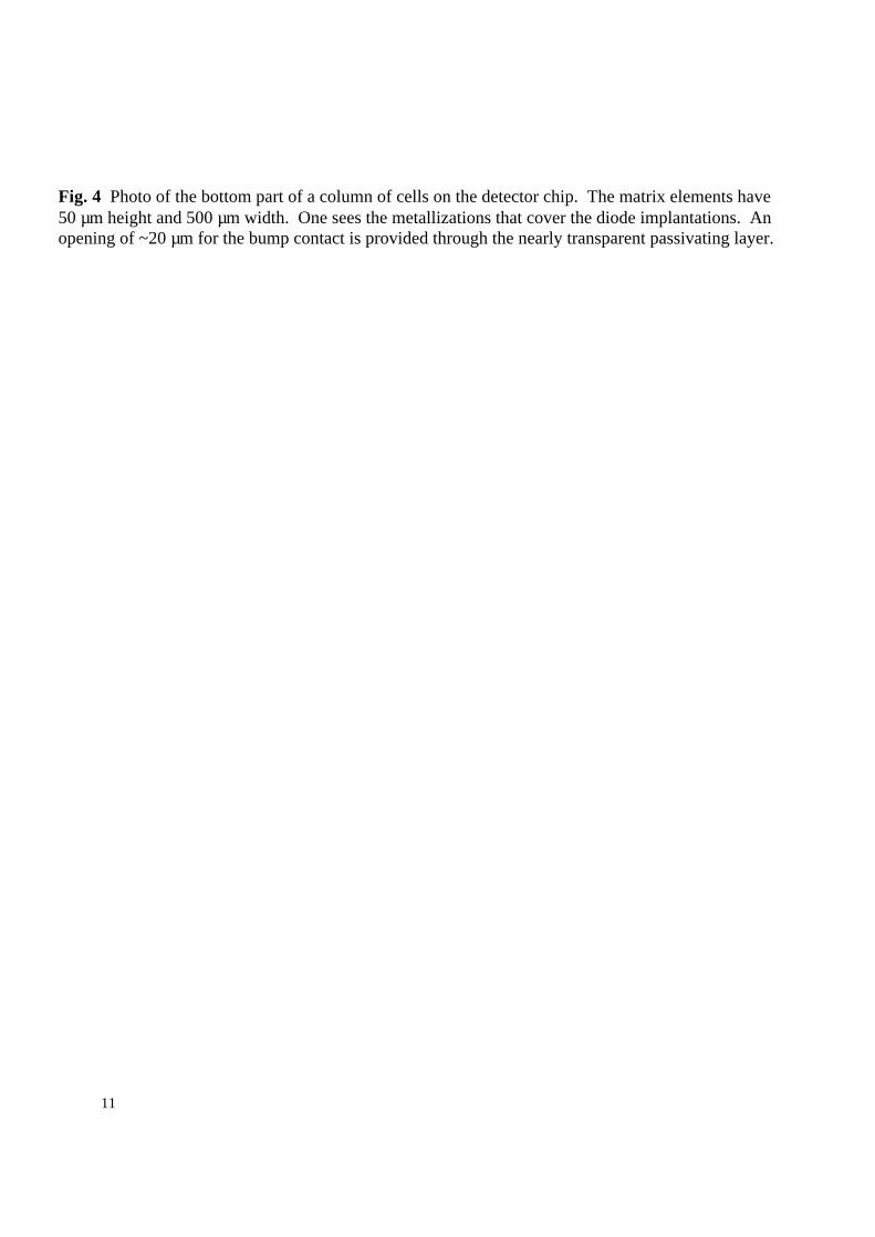
Fig. 4 Photo of the bottom part of a column of cells on the detector chip. The matrix elements have50 µm height and 500 µm width. One sees the metallizations that cover the diode implantations. Anopening of ~20 µm for the bump contact is provided through the nearly transparent passivating layer.
12
Input
Bias Current
Non-linear load
Coupling
Fig. 5. The comparator contains a bistable non-linear load and is ac coupled to minimize offset effects.
AAAAAAAAAAAAA
reset to preamp and comparator
IdlIdl
Idl Idl Idl Idl
IdlIdlIdl
Idl
Fig. 6. The main delay chain consist of 36 inverter stages. After the fourth stage the signal is fed back toreset pre amplifier and comparator. The effect of Idl is shown in fig. 11
13
4*I I2*I
B0B2 B1
dladladla
Fig. 7 The 3 bit delay trim is based on inverters which can be made current deprived or not by a switchacross the current sources. The Idla can be adjusted externally to set the trimming range between 60 nsand 300 ns.

14
Fig. 8 Photograph of the LHC1/Omega3 chip. One can distinguish 41 wire bonding pads at the bottom.
15
STROBELHC CLK
40 MHzL1
TRIGGERto chip-OR
to columnlow level logic column-OR
Fast OR DETECT
COINC LATCH
16 bit SHIFT REG
Fig. 9 Circuitry for fast-OR detection and time-stamping of hit columns at the bottom of each column.
16
0
50
100
150
Added Delay (ns)
0 5000 10000 15000 20000
Input Charge (e-)
Fig. 10 The added response time of a pixel cell due to timewalk in the discriminator for threshold settings
at 5000e-, 7000 e- and 9000 e-.
1000
1500
2000
2500
3000
3500
Delay (ns)
40 50 60 70 80 90 100 110
Idl (µA)
Fig. 11. Adjustment of the internal delay lines of the pixels can be achieved globally by varying the biascurrent Idl.
17
1800
1850
1900
1950
2000
2050
2100Delay (ns)
0 20 40 60 80 100 120Pixel Row Number(a)
1800
1850
1900
1950
2000
2050
2100Delay (ns)
0 20 40 60 80 100 120Pixel Row Number(b)
Fig. 12 The time response of 2000 pixels on one chip.(a) shows the time response before individual pixel delay correction. It indicates a random spread of~ 100 ns peak-to-peak on top of which are added systematic effects.(b) indicates that after correction of the delays in each pixel all pixels respond within a 25 ns time windowindicating a timing precision of better than 6 ns rms.
18
0
25
50
75
100Pixel Response (%)
3000 4000 5000 6000 7000 8000Input Charge (e-)
Fig. 13. The proportion of positive responses of pixels in the test rowas a function of input signal height in
steps of 50 e- equivalent at a nominal threshold Ith = 10 µA, ~5 000 e-.
5 10 15 20 25
Ith (µA)
2500
5000
7500
10000
12500
15000
Input charge (e-)
Fig 14. Variation of the threshold plotted against the current Ith. It can be noted that there is one channel(ch 0) which behaves differently from the others which may just be incidental. The symbols correspond tothose in fig. 13
19
0
10
20
30
40
10 15 20 25
Ithr [ µA]
thre
shol
d[100
0 e- ]
Fig. 15 A calibration of the electrical test measurements on one pixel channel using 3 photon sources
(marked with a circle). These were 109Cd (22 keV and 25 keV) 241Am (60 keV) and 57Co (122 keV).
row
col
0
25
50
75
100
125
0 5 10 15
Fig. 16. A scatter plot of hits recorded using a random trigger and a 90Sr source. Each pixel has around8 000 hits.
Related Documents