Power Integrations 5245 Hellyer Avenue, San Jose, CA 95138 USA. Tel: +1 408 414 9200 Fax: +1 408 414 9201 www.powerint.com DESIGN EXAMPLE REPORT Title 4.2 W Non-Isolated LED Driver LNK605DG Specification 85 – 265 VAC Input; 12 V, 350 mA Output Application LED Driver Author Applications Engineering Department Document Number DER-186 Date September 10, 2008 Revision 1.1 Summary and Features • Accurate primary-side constant voltage, constant current (CV/CC) controller eliminates optocoupler and all secondary side CV/CC control circuitry • ±5% output voltage and ±10% output current accuracy including line, load, temperature, and component tolerances • No current-sense resistors for maximized efficiency • Low part-count solution for lower cost • Auto-restart for output short circuit and open-loop protection • EcoSmart ® – Easily meets all existing and proposed international energy efficiency standards – China (CECP) / CEC / EPA / European Commission • ON/OFF control provides constant efficiency to very light loads • No-load consumption <200 mW at 265 VAC • Ultra-low leakage current: <5 μA at 265 VAC input (no Y capacitor required) • Easy compliance to EN550015 and CISPR-22 Class B EMI • Meets ENERGY STAR requirements for Solid State Lighting (SSL) luminaries • Green package: halogen free and RoHS compliant PATENT INFORMATION The products and applications illustrated herein (including transformer construction and circuits external to the products) may be covered by one or more U.S. and foreign patents, or potentially by pending U.S. and foreign patent applications assigned to Power Integrations. A complete list of Power Integrations' patents may be found at www.powerint.com. Power Integrations grants its customers a license under certain patent rights as set forth at <http://www.powerint.com/ip.htm>.

LED driver
Dec 22, 2015
4.2 watt rugged LED driver based on POWER INTEGRATION ...device
Welcome message from author
This document is posted to help you gain knowledge. Please leave a comment to let me know what you think about it! Share it to your friends and learn new things together.
Transcript

Power Integrations
5245 Hellyer Avenue, San Jose, CA 95138 USA. Tel: +1 408 414 9200 Fax: +1 408 414 9201
www.powerint.com
DESIGN EXAMPLE REPORT
Title 4.2 W Non-Isolated LED Driver LNK605DG
Specification 85 – 265 VAC Input; 12 V, 350 mA Output
Application LED Driver
Author Applications Engineering Department
Document Number
DER-186
Date September 10, 2008
Revision 1.1
Summary and Features
• Accurate primary-side constant voltage, constant current (CV/CC) controller eliminates optocoupler and all secondary side CV/CC control circuitry
• ±5% output voltage and ±10% output current accuracy including line, load, temperature, and component tolerances
• No current-sense resistors for maximized efficiency
• Low part-count solution for lower cost
• Auto-restart for output short circuit and open-loop protection
• EcoSmart® – Easily meets all existing and proposed international energy efficiency standards – China (CECP) / CEC / EPA / European Commission
• ON/OFF control provides constant efficiency to very light loads
• No-load consumption <200 mW at 265 VAC
• Ultra-low leakage current: <5 µA at 265 VAC input (no Y capacitor required)
• Easy compliance to EN550015 and CISPR-22 Class B EMI
• Meets ENERGY STAR requirements for Solid State Lighting (SSL) luminaries
• Green package: halogen free and RoHS compliant
PATENT INFORMATION The products and applications illustrated herein (including transformer construction and circuits external to the products) may be covered by one or more U.S. and foreign patents, or potentially by pending U.S. and foreign patent applications assigned to Power Integrations. A complete list of Power Integrations' patents may be found at www.powerint.com. Power Integrations grants its customers a license under certain patent rights as set forth at <http://www.powerint.com/ip.htm>.

DER-186 – 12 V, 350 mA LED Driver 10-Sep-08
Page 2 of 32
Power Integrations Tel: +1 408 414 9200 Fax: +1 408 414 9201 www.powerint.com
Table of Contents 1 Introduction.................................................................................................................3 2 Prototype Photo..........................................................................................................4 3 Power Supply Specification ........................................................................................5 4 Schematic...................................................................................................................6 5 Circuit Description ......................................................................................................7
5.1 LNK605DG Operation .........................................................................................7 5.2 Input Filter ...........................................................................................................7 5.3 Tapped Buck Operation ......................................................................................7 5.4 Output Regulation ...............................................................................................8
6 PCB Layout ..............................................................................................................10 7 Bill of Materials .........................................................................................................11 8 Tapped-inductor Specifications ................................................................................12
8.1 Electrical Diagram .............................................................................................12 8.2 Electrical Specifications.....................................................................................12 8.3 Materials............................................................................................................12 8.4 Tapped Inductor Build Diagram.........................................................................13 8.5 Winding Instruction............................................................................................13
9 Design Spreadsheet .................................................................................................14 10 Performance Data.................................................................................................16
10.1 Efficiency with LED Load – Full Load ................................................................16 10.2 No-load Input Power..........................................................................................17 10.3 Output Characteristics.......................................................................................18 10.4 Thermal Performance........................................................................................18 10.5 Output Ripple Measurements............................................................................19
10.5.1 Ripple Measurement Technique ................................................................19 10.5.2 Measurement Results ................................................................................20
11 Output Current Ripple ...........................................................................................21 11.1 Load Current Ripple ..........................................................................................21 11.2 Inductor Current ................................................................................................22
12 Waveforms............................................................................................................24 12.1 Output Voltage Startup Profile...........................................................................24 12.2 Output Current Startup Profile ...........................................................................25 12.3 Drain Voltage and Current.................................................................................26
13 Transient Protection..............................................................................................28 14 Conducted EMI .....................................................................................................29 15 Revision History ....................................................................................................31
Important Note: Although this board is designed to satisfy safety isolation requirements, the engineering prototype has not been agency approved. Therefore, all testing should be performed using an isolation transformer to provide the AC input to the prototype board.
10-Sep-08 DER-186 – 12 V, 350 mA LED Driver
Page 3 of 32
Power Integrations Tel: +1 408 414 9200 Fax: +1 408 414 9201
www.powerint.com
1 Introduction
This engineering report describes the design for a non-isolated, universal input, 12 V, 350 mA constant voltage/constant current (CV/CC) power supply for LED driver applications, utilizing a LNK605DG device from the LinkSwitch-II family in a tapped-inductor buck configuration. A tapped buck topology is ideal for converters with a high ratio of voltage input to voltage output. This topology provides current multiplication on the output, making it possible to use smaller devices, or to lower dissipation losses in the MOSFET. The tapped buck, non-isolated topology used in this design lends itself to advantages such as smaller PCB size, a smaller transformer, and greater efficiency than in the flyback topologies described in DER-184 and DER-185 (also using LinkSwitch-II devices.) The worst-case full load efficiency for this design is 80%, which is an improvement over the 74% efficiency of the previous two DER solutions. The EMI filtering is simpler in this buck topology, since there is far less common-mode noise, and lends itself to using fewer components. This design operates primarily in CC mode; CV mode only occurs when the load is disconnected, allowing the supply to operate in a safe mode, indefinitely, with the LED load disconnected. This document contains the power supply design’s specifications, schematic, bill of materials, inductor specifications, and typical performance characteristics.
DER-186 – 12 V, 350 mA LED Driver 10-Sep-08
Page 4 of 32
Power Integrations Tel: +1 408 414 9200 Fax: +1 408 414 9201 www.powerint.com
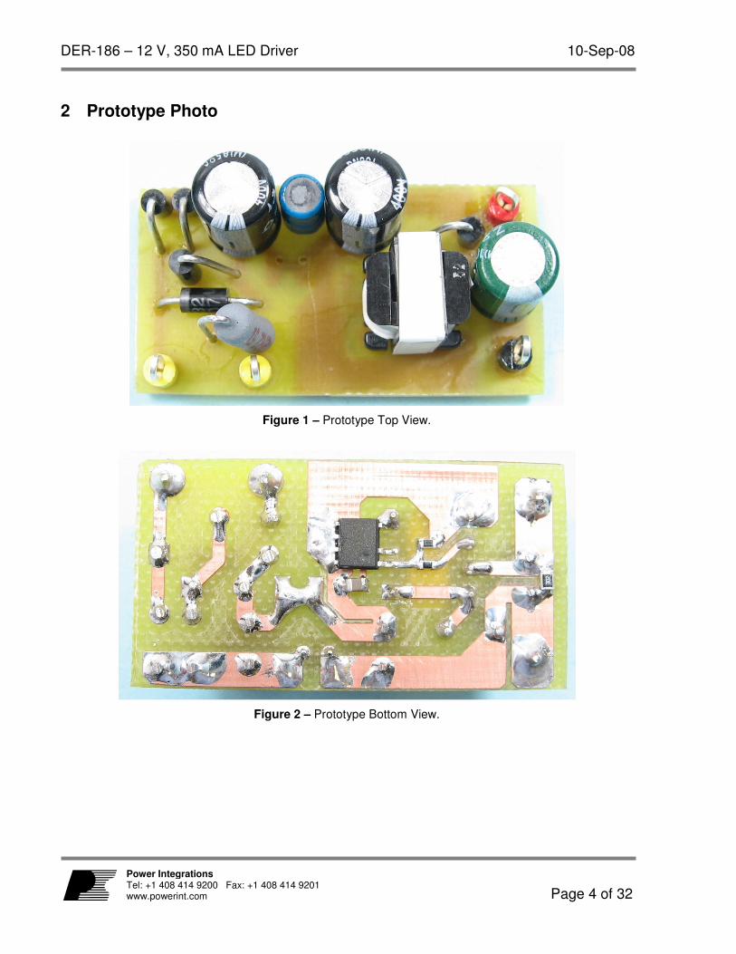
2 Prototype Photo
Figure 1 – Prototype Top View.
Figure 2 – Prototype Bottom View.

10-Sep-08 DER-186 – 12 V, 350 mA LED Driver
Page 5 of 32
Power Integrations Tel: +1 408 414 9200 Fax: +1 408 414 9201
www.powerint.com
3 Power Supply Specification
Description Symbol Min Typ Max Units Comment
Input
Voltage VIN 85 265 VAC 2 Wire – no P.E.
Frequency fLINE 47 50/60 64 Hz
No-load Input Power (230 VAC) 300 mW
Output
Output Voltage 1 VOUT1 12 V Measured at the output capacitor
Output Ripple Voltage 1 VRIPPLE1 300 mV 20 MHz bandwidth
Output Current 1 IOUT1 350 mA
Total Output Power
Continuous Output Power POUT 4.2 W
Efficiency
Full Load η 80 %
Environmental
Conducted EMI Meets CISPR22B / EN55022B
Safety Designed to meet IEC950, UL1950
Class II
Surge 2 kV
1.2/50 µs surge, IEC 1000-4-5, Series Impedance:
Differential Mode: 2 Ω
Common Mode: 12 Ω
Ambient Temperature TAMB -5 50 oC Free convection, sea level
DER-186 – 12 V, 350 mA LED Driver 10-Sep-08
Page 6 of 32
Power Integrations Tel: +1 408 414 9200 Fax: +1 408 414 9201 www.powerint.com
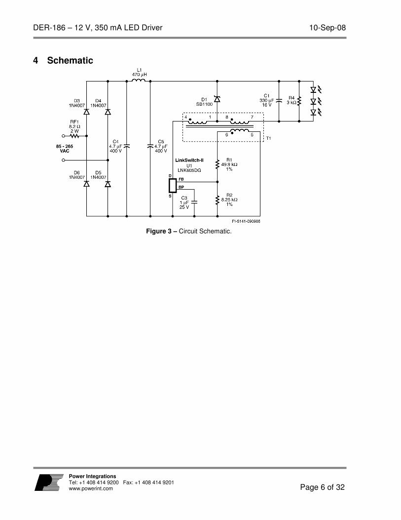
4 Schematic
Figure 3 – Circuit Schematic.

10-Sep-08 DER-186 – 12 V, 350 mA LED Driver
Page 7 of 32
Power Integrations Tel: +1 408 414 9200 Fax: +1 408 414 9201
www.powerint.com
5 Circuit Description
This circuit uses the LinkSwitch-II family product LNK605DG in a non-isolated tapped buck power-supply configuration. The LNK605DG device (U1) incorporates a power switching device, an oscillator, a CV/CC control engine, and startup and protection functions all in one IC. The integrated 700 V MOSFET allows sufficient voltage margin for universal input AC applications. The power supply delivers full output current during the maximum forward voltage drop of the LED. The LNK605DG’s IC package provides extended distance between high and low voltage pins (both at the package and the PCB), which is required in very humid or highly polluted environments to prevent arcing and to further improve reliability.
5.1 LNK605DG Operation
The LNK605DG monolithically integrates a 700 V power MOSFET switch and ON/OFF control. The constant voltage (CV) regulation provides ±5% accuracy. The CV function is not needed during normal operation in this application. The CV feature provides inherent output over-voltage protection in case any LEDs fail open circuit or if the load becomes disconnected. Beyond the maximum power point, the switching frequency is reduced to provide a constant output current at an accuracy of ±10%. This makes the LNK605DG ideal for driving LEDs, which require a constant current level for consistent light output and long life operation. In addition, internal compensation allows the ±5% voltage and ±10% current accuracies to be met across component tolerances, device tolerances, temperature, and line input voltage variations. The LNK605DG also provides a sophisticated range of protection features such as auto-restart and thermal shutdown. Auto-restart is triggered by fault conditions which include an open feedback loop or a shorted output. Accurate hysteretic thermal shutdown ensures safe average PCB temperatures under all conditions.
5.2 Input Filter
Diodes D3, D4, D5, and D6 rectify the AC input. The resulting DC is filtered by the bulk storage capacitors, C4 and C5. Inductor L1 and capacitors C4 and C5 form a pi (π) filter, which attenuates conducted differential-mode EMI noise. This configuration enables easy compliance to EMI standard EN55015 class B, with 10 dB of margin. Fusible, flameproof resistor RF1 acts as a fuse and should be rated to withstand the instantaneous dissipation when the supply is first connected to the AC. Wire-wound or oversized metal-film resistors work well for this purpose.
5.3 Tapped Buck Operation
Figure 3 shows the schematic for a tapped buck converter, based on the LNK605DG. A power supply using a tapped buck topology operates in a way very similar to one with a buck topology. When the switch turns on (closes), current ramps up and flows through

DER-186 – 12 V, 350 mA LED Driver 10-Sep-08
Page 8 of 32
Power Integrations Tel: +1 408 414 9200 Fax: +1 408 414 9201 www.powerint.com
the complete inductor (pin 7 to pin 4), and through the load (the LEDs). The load current is filtered by C1 to remove the switching component from the current waveform. Diode D1 is reverse-biased and so does not conduct during this time. The current continues to ramp up until it reaches the current limit value, which causes the switch to turn off (open). When the switch turns off, the energy in the input section of inductor (T1) couples through to the output section (pin 7 to pin 8). The peak current in the output winding steps up by a factor of 4.6 (equal to the ratio of total inductor turns to the output section turns), keeping the total ampere-turns constant. This stepped (magnified) current flows out of the output winding, through free-wheeling diode D1, and back through the load. (See Figure 16 though Figure 19.) Due to non-ideal coupling between the tapped windings, some of the stored energy does not couple to the output winding. The leakage energy in the input section of T1 (pin 4 to pin 1) causes a voltage spike at turn off. This spike is limited by the intra-winding capacitance of T1. This parasitic capacitance is sufficient to keep the voltage spike from exceeding the BVDSS (700 V) of the MOSFET internal to U1. The voltage stress on the switch in this design is equal to that in a Flyback converter using a transformer with the same turns ratio. The chosen turns ratio ensures the circuit operates in discontinuous mode (DCM) at low line (85 VAC). This ratio (the inductor ratio) can be calculated as
6.427
124===
TurnsWindingOutput
turnsInductorTotalRatioInductor
5.4 Output Regulation
The LNK605DG regulates output using ON/OFF control for CV regulation, and frequency control for constant current (CC) regulation. Feedback resistors R1 and R2 have 1% tolerance values to assist accurately centering both the nominal output voltage and the CC regulation threshold. The CV feature provides output over-voltage protection (OVP) in case any LEDs have open-circuit failures. This design operates primarily in CC mode, but it goes into CV mode below full load, or when the load is disconnected. A feedback winding tracks and regulates the output. This winding must be closely coupled to the tapped section (the section of winding between pin 7 and pin 8) of T1. Traversing from no load to full load, the controller within the LNK605DG first operates in CV mode. Upon detecting the maximum power point, the controller enters CC mode. While the LNK605DG operates in the CV region, it regulates the output voltage by adjusting the ratio of enabled cycles to disabled switching cycles. This also optimizes the efficiency of the converter over the entire load range. As the load current increases, the current limit is increased and fewer and fewer cycles are skipped.

10-Sep-08 DER-186 – 12 V, 350 mA LED Driver
Page 9 of 32
Power Integrations Tel: +1 408 414 9200 Fax: +1 408 414 9201
www.powerint.com
At the point where no switching cycles are skipped (concurrent to the maximum power point) the controller within the LinkSwitch-II transitions into CC mode. A further increase in the demand for load current causes the output voltage to drop. This drop in output voltage is reflected on the FB pin voltage. In response to the voltage reduction on the FB pin, the switching frequency is reduced to achieve constant output current.
DER-186 – 12 V, 350 mA LED Driver 10-Sep-08
Page 10 of 32
Power Integrations Tel: +1 408 414 9200 Fax: +1 408 414 9201 www.powerint.com
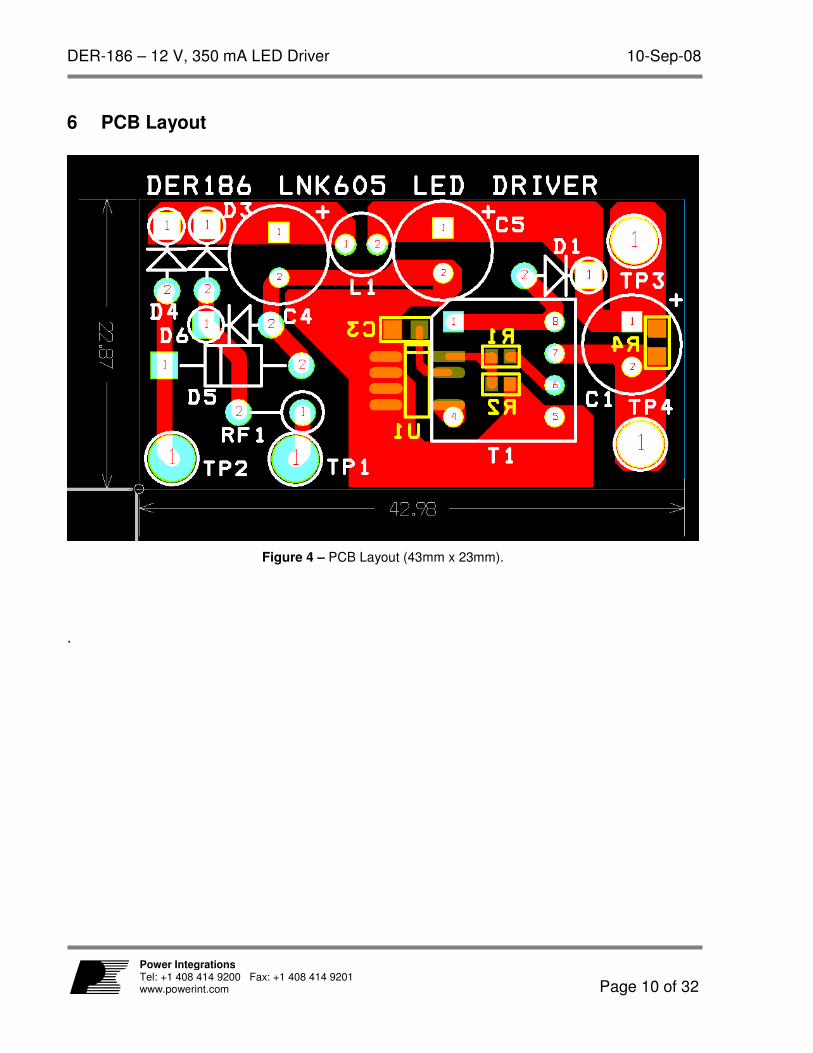
6 PCB Layout
Figure 4 – PCB Layout (43mm x 23mm).
.

10-Sep-08 DER-186 – 12 V, 350 mA LED Driver
Page 11 of 32
Power Integrations Tel: +1 408 414 9200 Fax: +1 408 414 9201
www.powerint.com
7 Bill of Materials Item Qty Ref Des Description Mfg Mfg Part Number
1 1 C1 330 µF, 16 V, Electrolytic, Very Low ESR, 72 mOhm, (8 x 11.5)
Nippon Chemi-Con EKZE160ELL331MHB5D
2 1 C3 1 µF, 25 V, Ceramic, X7R, 0805 Panasonic ECJ-2FB1E105K
3 2 C4 C5 4.7 µF, 400 V, Electrolytic, (8 x 11.5)
Taicon Corporation TAQ2G4R7MK0811MLL3
4 1 D1 100 V, 1 A, Schottky, DO-41 Vishay SB1100
5 4 D3 D4 D5 D6 1000 V, 1 A, Rectifier, DO-41 Vishay 1N4007-E3/54
6 1 L1 470 µH, 0.3 A, 5.5 x 10.5 mm Tokin SBC1-471-301
7 1 R1 49.9 kΩ, 1%, 1/16 W, Metal Film, 0603 Panasonic ERJ-3EKF4992V
8 1 R2 8.25 kΩ, 1%, 1/16 W, Metal Film, 0603 Panasonic ERJ-3EKF8251V
9 1 R4 3 kΩ, 5%, 1/8 W, Metal Film, 0805 Panasonic ERJ-6GEYJ302V
10 1 RF1 8.2 Ω, 2 W, Fusible/Flame Proof Vitrohm CRF253-4 5T 8R2
11 1 T1 Bobbin, EE10, Vertical, 8 pins Hical
Magnetics 101
12 2 TP1 TP4 Test Point, BLK,THRU-HOLE MOUNT Keystone 5011
13 1 TP2 Test Point, WHT,THRU-HOLE MOUNT Keystone 5012
14 1 TP3 Test Point, RED,THRU-HOLE MOUNT Keystone 5010
15 1 U1 LinkSwitch-II, LNK605DG, CV/CC, SO-8C
Power Integrations LNK605DG

DER-186 – 12 V, 350 mA LED Driver 10-Sep-08
Page 12 of 32
Power Integrations Tel: +1 408 414 9200 Fax: +1 408 414 9201 www.powerint.com
8 Tapped-inductor Specifications
8.1 Electrical Diagram
Figure 5 – Transformer Electrical Diagram.
8.2 Electrical Specifications
Electrical Strength 1 second, 60 Hz, from Primary to Secondary N/A
Main Inductance Pins 4 - 7, short Pin 1 and Pin 8 together, measured at 80 kHz, 0.4 VRMS
1.32 mH, ±10%
Resonant Frequency Pins 4 - 7, Pin 1 and Pin 8 are shorted together with all other windings open
1.1 MHz
Primary Leakage Inductance Pin 4 to pin 1, Pin 7 and Pin 8 are shorted together
18 µH
8.3 Materials
Item Description
[1] Core: PC44, gapped for AL of 86.3 nH/t2
[2] Bobbin: Horizontal 8 pin, EE10 [3] Magnet Wire: #34 AWG [4] Magnet Wire: #27 AWG [5] Magnet Wire: #33 AWG [6] Tape, 3M 1298 Polyester Film, 2.0 Mils thick, 7.0 mm wide [7] Varnish

10-Sep-08 DER-186 – 12 V, 350 mA LED Driver
Page 13 of 32
Power Integrations Tel: +1 408 414 9200 Fax: +1 408 414 9201
www.powerint.com
8.4 Tapped Inductor Build Diagram
Figure 6 – Transformer Build Diagram.
8.5 Winding Instruction
WD1 Main Winding
Primary Pin side of the bobbin oriented to right hand side. Start at pin 4. Wind 97 turns of item [3] in three layers. Wind with tight tension across bobbin evenly. End at pin 1.
Insulation 1 Layer of tape [6] for insulation.
WD #2 Tap Winding
Start at pin 8. Wind 27 turns of item [4] in two layers. Terminate on pin 7. Wind with tight tension and spread turns across bobbin evenly.
Insulation 1 layer of tape [6] for basic insulation.
WD #3 Feedback Winding
Starting at pin 6, wind 27 turns of item [5] in one layer. Finish on pin 5. Wind with tight tension and spread turns across bobbin evenly.
Insulation 2 layers of tape [6] for basic insulation.
Core Assembly Gap core and assemble and secure core halves.
Varnish Dip varnish assembly with item [7].
DER-186 – 12 V, 350 mA LED Driver 10-Sep-08
Page 14 of 32
Power Integrations Tel: +1 408 414 9200 Fax: +1 408 414 9201 www.powerint.com
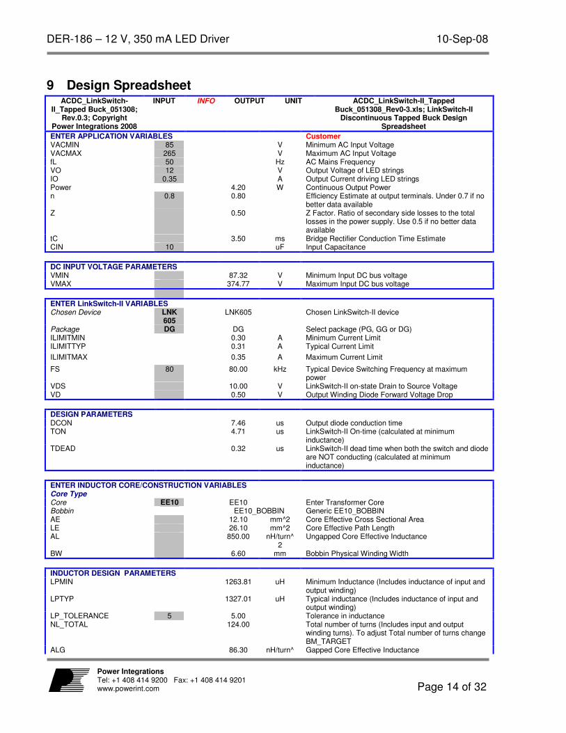
9 Design Spreadsheet ACDC_LinkSwitch-
II_Tapped Buck_051308; Rev.0.3; Copyright
Power Integrations 2008
INPUT INFO OUTPUT UNIT ACDC_LinkSwitch-II_Tapped Buck_051308_Rev0-3.xls; LinkSwitch-II
Discontinuous Tapped Buck Design Spreadsheet
ENTER APPLICATION VARIABLES Customer VACMIN 85 V Minimum AC Input Voltage VACMAX 265 V Maximum AC Input Voltage fL 50 Hz AC Mains Frequency VO 12 V Output Voltage of LED strings IO 0.35 A Output Current driving LED strings Power 4.20 W Continuous Output Power n 0.8 0.80 Efficiency Estimate at output terminals. Under 0.7 if no
better data available Z 0.50 Z Factor. Ratio of secondary side losses to the total
losses in the power supply. Use 0.5 if no better data available
tC 3.50 ms Bridge Rectifier Conduction Time Estimate CIN 10 uF Input Capacitance
DC INPUT VOLTAGE PARAMETERS VMIN 87.32 V Minimum Input DC bus voltage VMAX 374.77 V Maximum Input DC bus voltage
ENTER LinkSwitch-II VARIABLES Chosen Device LNK
605 LNK605 Chosen LinkSwitch-II device
Package DG DG Select package (PG, GG or DG) ILIMITMIN 0.30 A Minimum Current Limit ILIMITTYP 0.31 A Typical Current Limit
ILIMITMAX 0.35 A Maximum Current Limit
FS 80 80.00 kHz Typical Device Switching Frequency at maximum power
VDS 10.00 V LinkSwitch-II on-state Drain to Source Voltage VD 0.50 V Output Winding Diode Forward Voltage Drop
DESIGN PARAMETERS DCON 7.46 us Output diode conduction time TON 4.71 us LinkSwitch-II On-time (calculated at minimum
inductance) TDEAD 0.32 us LinkSwitch-II dead time when both the switch and diode
are NOT conducting (calculated at minimum inductance)
ENTER INDUCTOR CORE/CONSTRUCTION VARIABLES Core Type Core EE10 EE10 Enter Transformer Core Bobbin EE10_BOBBIN Generic EE10_BOBBIN AE 12.10 mm^2 Core Effective Cross Sectional Area LE 26.10 mm^2 Core Effective Path Length AL 850.00 nH/turn^
2 Ungapped Core Effective Inductance
BW 6.60 mm Bobbin Physical Winding Width
INDUCTOR DESIGN PARAMETERS LPMIN 1263.81 uH Minimum Inductance (Includes inductance of input and
output winding) LPTYP 1327.01 uH Typical inductance (Includes inductance of input and
output winding) LP_TOLERANCE 5 5.00 Tolerance in inductance NL_TOTAL 124.00 Total number of turns (Includes input and output
winding turns). To adjust Total number of turns change BM_TARGET
ALG 86.30 nH/turn^ Gapped Core Effective Inductance
10-Sep-08 DER-186 – 12 V, 350 mA LED Driver
Page 15 of 32
Power Integrations Tel: +1 408 414 9200 Fax: +1 408 414 9201
www.powerint.com
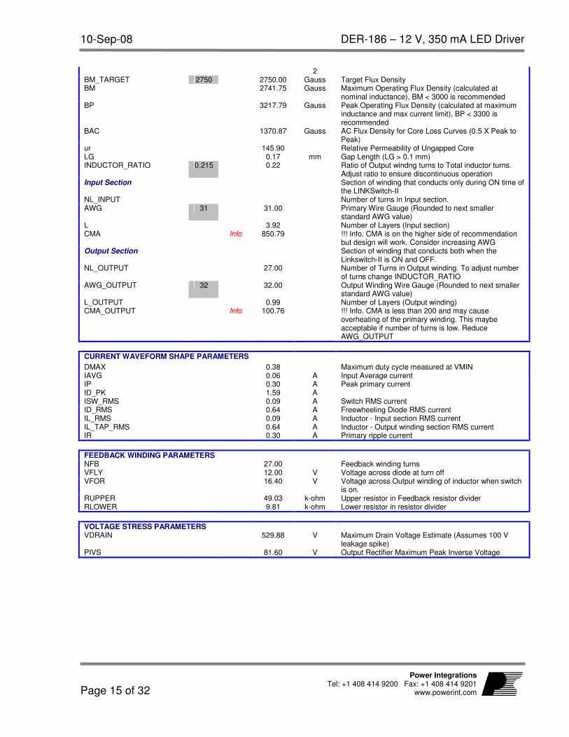
2 BM_TARGET 2750 2750.00 Gauss Target Flux Density BM 2741.75 Gauss Maximum Operating Flux Density (calculated at
nominal inductance), BM < 3000 is recommended BP 3217.79 Gauss Peak Operating Flux Density (calculated at maximum
inductance and max current limit), BP < 3300 is recommended
BAC 1370.87 Gauss AC Flux Density for Core Loss Curves (0.5 X Peak to Peak)
ur 145.90 Relative Permeability of Ungapped Core LG 0.17 mm Gap Length (LG > 0.1 mm) INDUCTOR_RATIO 0.215 0.22 Ratio of Output windng turns to Total inductor turns.
Adjust ratio to ensure discontinuous operation Input Section Section of winding that conducts only during ON time of
the LINKSwitch-II NL_INPUT Number of turns in Input section. AWG 31 31.00 Primary Wire Gauge (Rounded to next smaller
standard AWG value) L 3.92 Number of Layers (Input section) CMA Info 850.79 !!! Info. CMA is on the higher side of recommendation
but design will work. Consider increasing AWG Output Section Section of winding that conducts both when the
Linkswitch-II is ON and OFF. NL_OUTPUT 27.00 Number of Turns in Output winding. To adjust number
of turns change INDUCTOR_RATIO AWG_OUTPUT 32 32.00 Output Winding Wire Gauge (Rounded to next smaller
standard AWG value) L_OUTPUT 0.99 Number of Layers (Output winding) CMA_OUTPUT Info 100.76 !!! Info. CMA is less than 200 and may cause
overheating of the primary winding. This maybe acceptable if number of turns is low. Reduce AWG_OUTPUT
CURRENT WAVEFORM SHAPE PARAMETERS
DMAX 0.38 Maximum duty cycle measured at VMIN IAVG 0.06 A Input Average current IP 0.30 A Peak primary current ID_PK 1.59 A ISW_RMS 0.09 A Switch RMS current ID_RMS 0.64 A Freewheeling Diode RMS current IL_RMS 0.09 A Inductor - Input section RMS current IL_TAP_RMS 0.64 A Inductor - Output winding section RMS current IR 0.30 A Primary ripple current
FEEDBACK WINDING PARAMETERS NFB 27.00 Feedback winding turns VFLY 12.00 V Voltage across diode at turn off VFOR 16.40 V Voltage across Output winding of inductor when switch
is on. RUPPER 49.03 k-ohm Upper resistor in Feedback resistor divider RLOWER 9.81 k-ohm Lower resistor in resistor divider
VOLTAGE STRESS PARAMETERS VDRAIN 529.88 V Maximum Drain Voltage Estimate (Assumes 100 V
leakage spike) PIVS 81.60 V Output Rectifier Maximum Peak Inverse Voltage

DER-186 – 12 V, 350 mA LED Driver 10-Sep-08
Page 16 of 32
Power Integrations Tel: +1 408 414 9200 Fax: +1 408 414 9201 www.powerint.com
10 Performance Data
All measurements performed at room temperature, 60 Hz input frequency.
10.1 Efficiency with LED Load – Full Load
This data was taken using three 350 mA, 3.5 V LEDs connected in a series string.
Full Load Efficiency
50
55
60
65
70
75
80
85
85 115 145 175 205 235 265
Input Voltage (Vac)
Eff
icie
nc
y (
%)
Figure 7 – Full-load Efficiency vs Input Voltage.
10-Sep-08 DER-186 – 12 V, 350 mA LED Driver
Page 17 of 32
Power Integrations Tel: +1 408 414 9200 Fax: +1 408 414 9201
www.powerint.com
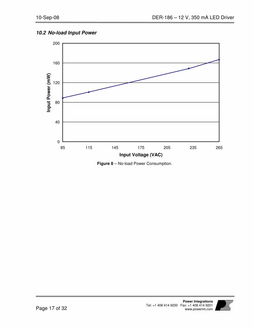
10.2 No-load Input Power
0
40
80
120
160
200
85 115 145 175 205 235 265
Input Voltage (VAC)
Inp
ut
Po
wer
(mW
)
Figure 8 – No-load Power Consumption.
DER-186 – 12 V, 350 mA LED Driver 10-Sep-08
Page 18 of 32
Power Integrations Tel: +1 408 414 9200 Fax: +1 408 414 9201 www.powerint.com
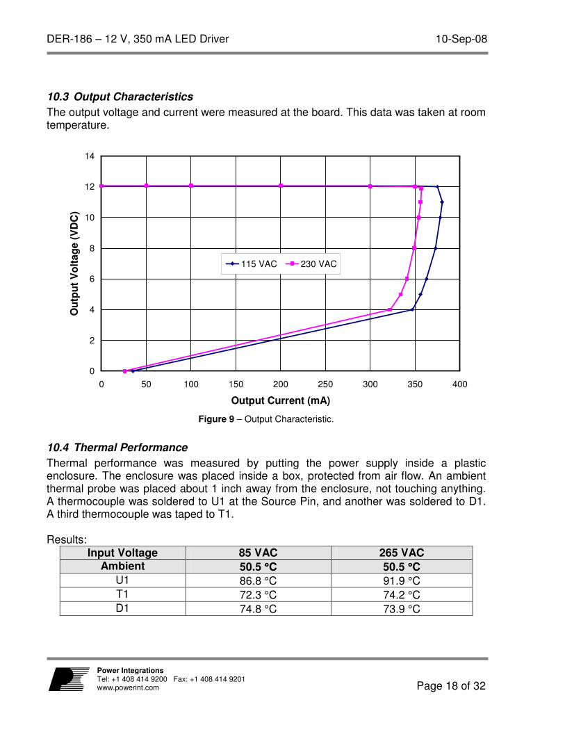
10.3 Output Characteristics
The output voltage and current were measured at the board. This data was taken at room temperature.
0
2
4
6
8
10
12
14
0 50 100 150 200 250 300 350 400
Output Current (mA)
Ou
tpu
t V
olt
ag
e (
VD
C)
115 VAC 230 VAC
Figure 9 – Output Characteristic.
10.4 Thermal Performance
Thermal performance was measured by putting the power supply inside a plastic enclosure. The enclosure was placed inside a box, protected from air flow. An ambient thermal probe was placed about 1 inch away from the enclosure, not touching anything. A thermocouple was soldered to U1 at the Source Pin, and another was soldered to D1. A third thermocouple was taped to T1. Results:
Input Voltage 85 VAC 265 VAC Ambient 50.5 °°°°C 50.5 °°°°C
U1 86.8 °C 91.9 °C T1 72.3 °C 74.2 °C D1 74.8 °C 73.9 °C

10-Sep-08 DER-186 – 12 V, 350 mA LED Driver
Page 19 of 32
Power Integrations Tel: +1 408 414 9200 Fax: +1 408 414 9201
www.powerint.com
10.5 Output Ripple Measurements
10.5.1 Ripple Measurement Technique
For DC output ripple measurements, use a modified oscilloscope test probe to reduce spurious signals. Details of the probe modification are provided in figures below. Tie two capacitors in parallel across the probe tip of the 4987BA probe adapter. Use a
0.1 µF/50 V ceramic capacitor and a 1.0 µF/50 V aluminum-electrolytic capacitor. The aluminum-electrolytic capacitor is polarized, so always maintain proper polarity across DC outputs.
Figure 10 – Oscilloscope Probe Prepared for Ripple Measurement. (End Cap and Ground Lead Removed)
Figure 11 – Oscilloscope Probe with Probe Master 4987BA BNC Adapter. (Modified with wires for probe ground for ripple measurement, and two parallel decoupling capacitors added)
Probe Ground
Probe Tip

DER-186 – 12 V, 350 mA LED Driver 10-Sep-08
Page 20 of 32
Power Integrations Tel: +1 408 414 9200 Fax: +1 408 414 9201 www.powerint.com
10.5.2 Measurement Results
Figure 12 – Output Ripple and Noise at 115 VAC Input with LED Load.
Figure 13 – Output Ripple and Noise at 230 VAC Input with LED Load.

10-Sep-08 DER-186 – 12 V, 350 mA LED Driver
Page 21 of 32
Power Integrations Tel: +1 408 414 9200 Fax: +1 408 414 9201
www.powerint.com
11 Output Current Ripple
11.1 Load Current Ripple
The following oscillograms show the AC component in the load current. LEDs were used as the load.
Figure 14 – Output Current Ripple at 115 VAC Input. Current: 10 mA/div, 10 µs/div.
Figure 15 – Output Current Ripple at 230 VAC. Current: 10 mA/div, 10 µs/div.

DER-186 – 12 V, 350 mA LED Driver 10-Sep-08
Page 22 of 32
Power Integrations Tel: +1 408 414 9200 Fax: +1 408 414 9201 www.powerint.com
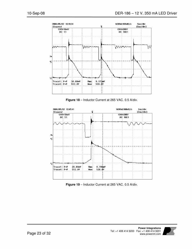
11.2 Inductor Current
The inductor current over the entire switching cycle is shown in the following four oscillograms. 3 series-connected LEDs were used as the load. At turn off the current in the inductor increases by a factor of 4.6 (corresponding to the turns ratio).
Figure 16 – Inductor Current at 85 VAC. 0.5 A/div.
Figure 17 – Inductor Current at 85 VAC. 0.5 A/div.
10-Sep-08 DER-186 – 12 V, 350 mA LED Driver
Page 23 of 32
Power Integrations Tel: +1 408 414 9200 Fax: +1 408 414 9201
www.powerint.com
Figure 18 – Inductor Current at 265 VAC. 0.5 A/div.
Figure 19 – Inductor Current at 265 VAC. 0.5 A/div.
DER-186 – 12 V, 350 mA LED Driver 10-Sep-08
Page 24 of 32
Power Integrations Tel: +1 408 414 9200 Fax: +1 408 414 9201 www.powerint.com
12 Waveforms
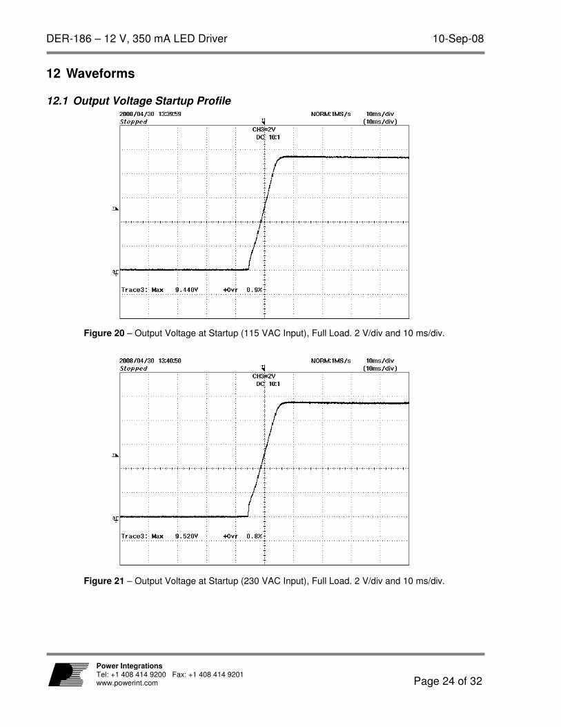
12.1 Output Voltage Startup Profile
Figure 20 – Output Voltage at Startup (115 VAC Input), Full Load. 2 V/div and 10 ms/div.
Figure 21 – Output Voltage at Startup (230 VAC Input), Full Load. 2 V/div and 10 ms/div.

10-Sep-08 DER-186 – 12 V, 350 mA LED Driver
Page 25 of 32
Power Integrations Tel: +1 408 414 9200 Fax: +1 408 414 9201
www.powerint.com
12.2 Output Current Startup Profile
Figure 22 – LED Current at Startup (115 VAC), Full Load. 100 mA/div and 10 ms/div.
Figure 23 – LED Current at Startup (230 VAC), Full Load. 100 mA/div and 10 ms/div.
DER-186 – 12 V, 350 mA LED Driver 10-Sep-08
Page 26 of 32
Power Integrations Tel: +1 408 414 9200 Fax: +1 408 414 9201 www.powerint.com
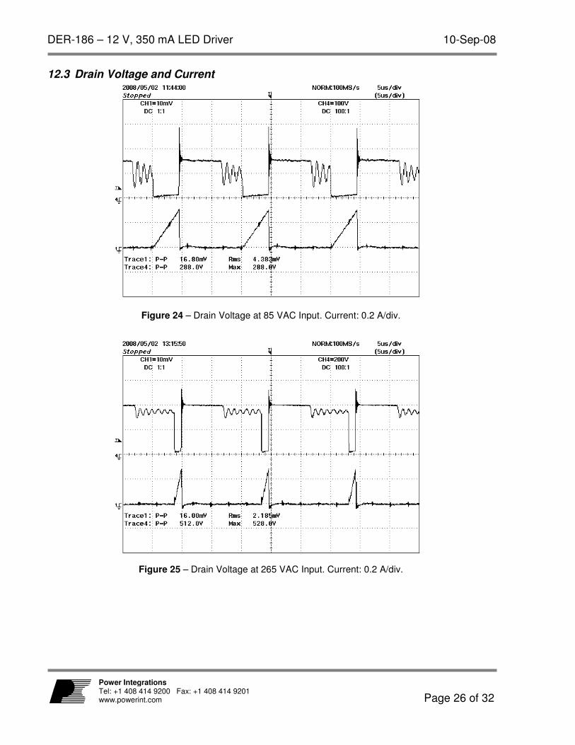
12.3 Drain Voltage and Current
Figure 24 – Drain Voltage at 85 VAC Input. Current: 0.2 A/div.
Figure 25 – Drain Voltage at 265 VAC Input. Current: 0.2 A/div.

10-Sep-08 DER-186 – 12 V, 350 mA LED Driver
Page 27 of 32
Power Integrations Tel: +1 408 414 9200 Fax: +1 408 414 9201
www.powerint.com
Figure 26 – Drain Voltage During Startup at 265 VAC. 100 V/div and 10 ms/div.

DER-186 – 12 V, 350 mA LED Driver 10-Sep-08
Page 28 of 32
Power Integrations Tel: +1 408 414 9200 Fax: +1 408 414 9201 www.powerint.com
13 Transient Protection
Energy Star line-transient protection requires immunity to 7 strikes of a 100 kHz ring wave, 2.5 kV level, for both common mode and differential mode. The following tests were performed at 230 VAC input, at both 90 ° and 270 ° phase. Differential Mode
Phase Voltage Current Results
90 Degree 2.5 kV 500 A Pass
270 Degree 2.5 kV 500 A Pass
Common Mode
Phase Voltage Current Results
90 Degree 2.5 kV 500 A Pass
270 Degree 2.5 kV 500 A Pass

10-Sep-08 DER-186 – 12 V, 350 mA LED Driver
Page 29 of 32
Power Integrations Tel: +1 408 414 9200 Fax: +1 408 414 9201
www.powerint.com
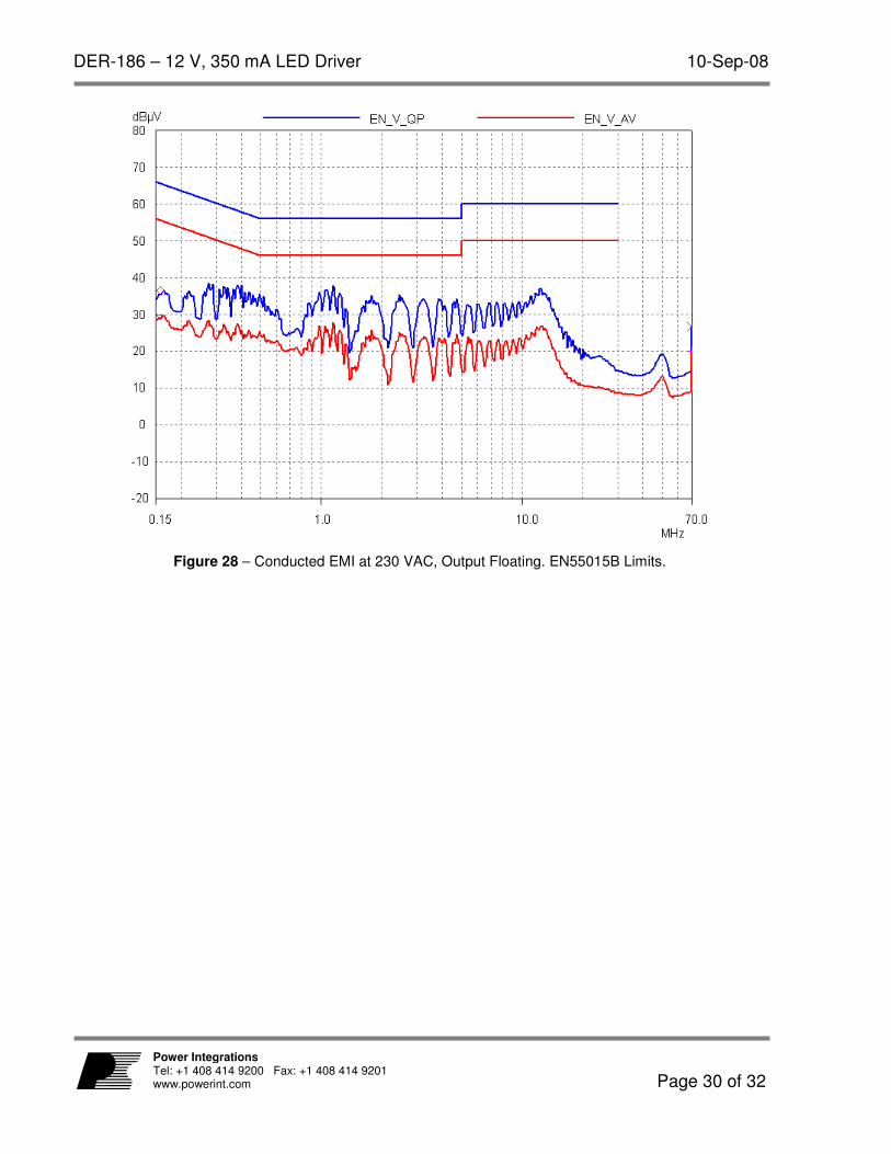
14 Conducted EMI
Figure 27 – Conducted EMI at 115 VAC, Output Floating. EN55015B Limits.
DER-186 – 12 V, 350 mA LED Driver 10-Sep-08
Page 30 of 32
Power Integrations Tel: +1 408 414 9200 Fax: +1 408 414 9201 www.powerint.com
Figure 28 – Conducted EMI at 230 VAC, Output Floating. EN55015B Limits.

10-Sep-08 DER-186 – 12 V, 350 mA LED Driver
Page 31 of 32
Power Integrations Tel: +1 408 414 9200 Fax: +1 408 414 9201
www.powerint.com
15 Revision History
Date Author Revision Description & changes Reviewed 15-May-08 SGK 1.0 Initial Release JD 10-Sep-08 SGK 1.1 Updated Schematic KM

DER-186 – 12 V, 350 mA LED Driver 10-Sep-08
Page 32 of 32
Power Integrations Tel: +1 408 414 9200 Fax: +1 408 414 9201 www.powerint.com
For the latest updates, visit our website: www.powerint.com
Power Integrations reserves the right to make changes to its products at any time to improve reliability or
manufacturability. Power Integrations does not assume any liability arising from the use of any device or circuit
described herein. POWER INTEGRATIONS MAKES NO WARRANTY HEREIN AND SPECIFICALLY DISCLAIMS ALL
WARRANTIES INCLUDING, WITHOUT LIMITATION, THE IMPLIED WARRANTIES OF MERCHANTABILITY,
FITNESS FOR A PARTICULAR PURPOSE, AND NON-INFRINGEMENT OF THIRD PARTY RIGHTS.
PATENT INFORMATION
The products and applications illustrated herein (including transformer construction and circuits external to the products)
may be covered by one or more U.S. and foreign patents, or potentially by pending U.S. and foreign patent applications
assigned to Power Integrations. A complete list of Power Integrations’ patents may be found at www.powerint.com.
Power Integrations grants its customers a license under certain patent rights as set forth at
http://www.powerint.com/ip.htm.
The PI Logo, TOPSwitch, TinySwitch, LinkSwitch, DPA-Switch, PeakSwitch, EcoSmart, Clampless, E-Shield, Filterfuse, StackFET,
PI Expert and PI FACTS are trademarks of Power Integrations, Inc. Other trademarks are property of their respective
companies. ©Copyright 2008 Power Integrations, Inc.
Power Integrations Worldwide Sales Support Locations
WORLD HEADQUARTERS 5245 Hellyer Avenue San Jose, CA 95138, USA. Main: +1-408-414-9200 Customer Service: Phone: +1-408-414-9665 Fax: +1-408-414-9765 e-mail: [email protected]
GERMANY Rueckertstrasse 3 D-80336, Munich Germany Phone: +49-89-5527-3911 Fax: +49-89-5527-3920 e-mail: [email protected]
JAPAN Kosei Dai-3 Bldg., 2-12-11, Shin-Yokohama, Kohoku-ku, Yokohama-shi, Kanagawa 222-0033 Phone: +81-45-471-1021 Fax: +81-45-471-3717 e-mail: [email protected]
TAIWAN 5F, No. 318, Nei Hu Rd., Sec. 1 Nei Hu Dist. Taipei, Taiwan 114, R.O.C. Phone: +886-2-2659-4570 Fax: +886-2-2659-4550 e-mail: [email protected]
CHINA (SHANGHAI) Rm 1601/1610, Tower 1, Kerry Everbright City No. 218 Tianmu Road West, Shanghai, P.R.C. 200070 Phone: +86-21-6354-6323 Fax: +86-21-6354-6325 e-mail: [email protected]
INDIA #1, 14
th Main Road
Vasanthanagar Bangalore-560052 India Phone: +91-80-41138020 Fax: +91-80-41138023 e-mail: [email protected]
KOREA RM 602, 6FL Korea City Air Terminal B/D, 159-6 Samsung-Dong, Kangnam-Gu, Seoul, 135-728, Korea Phone: +82-2-2016-6610 Fax: +82-2-2016-6630 e-mail: [email protected]
UNITED KINGDOM 1st Floor, St. James’s House East Street, Farnham Surrey, GU9 7TJ United Kingdom Phone: +44 (0) 1252-730-141 Fax: +44 (0) 1252-727-689 e-mail: [email protected]
CHINA (SHENZHEN) Rm A, B & C 4
th Floor, Block C,
Electronics Science and Technology Building, 2070 Shennan Zhong Rd, Shenzhen, Guangdong, China, 518031 Phone: +86-755-8379-3243 Fax: +86-755-8379-5828 e-mail: [email protected]
ITALY Via De Amicis 2 20091 Bresso MI – Italy Phone: +39-028-928-6000 Fax: +39-028-928-6009 e-mail: [email protected]
SINGAPORE 51 Newton Road, #15-08/10 Goldhill Plaza, Singapore, 308900 Phone: +65-6358-2160 Fax: +65-6358-2015 e-mail: [email protected]
APPLICATIONS HOTLINE World Wide +1-408-414-9660 APPLICATIONS FAX World Wide +1-408-414-9760
Related Documents


