CSE 140: Components and Design Techniques for Digital Systems Lecture 7: Sequential Networks CK Cheng Dept. of Computer Science and Engineering University of California, San Diego 1

Welcome message from author
This document is posted to help you gain knowledge. Please leave a comment to let me know what you think about it! Share it to your friends and learn new things together.
Transcript
CSE 140: Components and Design Techniques for
Digital Systems
Lecture 7:
Sequential Networks
CK Cheng
Dept. of Computer Science and Engineering
University of California, San Diego
1

Part II: Sequential Networks
1. Introduction
1. Sequential circuits
2. Memory hierarchy
3. Basic mechanism of memory
2. Basic Building Blocks
1. Latches
2. Flip-Flops
3. Examples of Memory Modules
3. Implementation
1. Finite state machine2

1. Introduction: What is a sequential circuit?
3
“A circuit whose output depends on current inputs and past outputs”
“A circuit with memory”
Memory: a key parameter is Time
Memory / Time steps
Clock
𝑥i 𝑦i
𝑠i

1. Introduction: Sequential Network Key features
Memory: Flip flops
Specification: Finite State Machines
Implementation: Excitation Tables
Main Theme: Timing
Present time = t and next time = t+1
Timing constraints to separate the present and next times.
yi = fi(St,X)
sit+1= gi(S
t,X)
4
YX
Combinational
logic
StSt+1
clock
Memory / Time steps
Clock
xi yisi

1. Introduction: Sequential Network Key features
Main Theme: Timing
Present time = t and next time = t+1
Timing constraints to separate the present and next times.
yi = fi(St,X)
sit+1= gi(S
t,X)
5
YX
Combinational
logic
St
clock
YX
Combinational
logic
StSt+1
clock
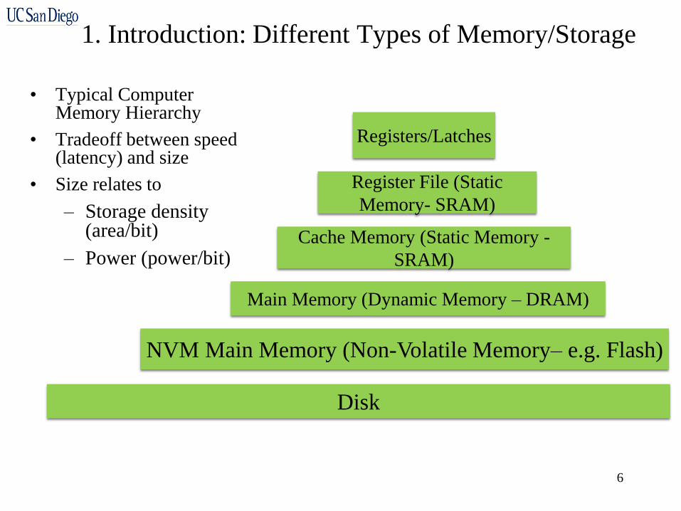
1. Introduction: Different Types of Memory/Storage
• Typical Computer Memory Hierarchy
• Tradeoff between speed (latency) and size
• Size relates to
– Storage density (area/bit)
– Power (power/bit)
6
Registers/Latches
Register File (Static
Memory- SRAM)
Cache Memory (Static Memory -
SRAM)
Main Memory (Dynamic Memory – DRAM)
NVM Main Memory (Non-Volatile Memory– e.g. Flash)
Disk

1. Introduction: Fundamental Memory Mechanism
QQQ
Q
I1
I2
I2 I1
7
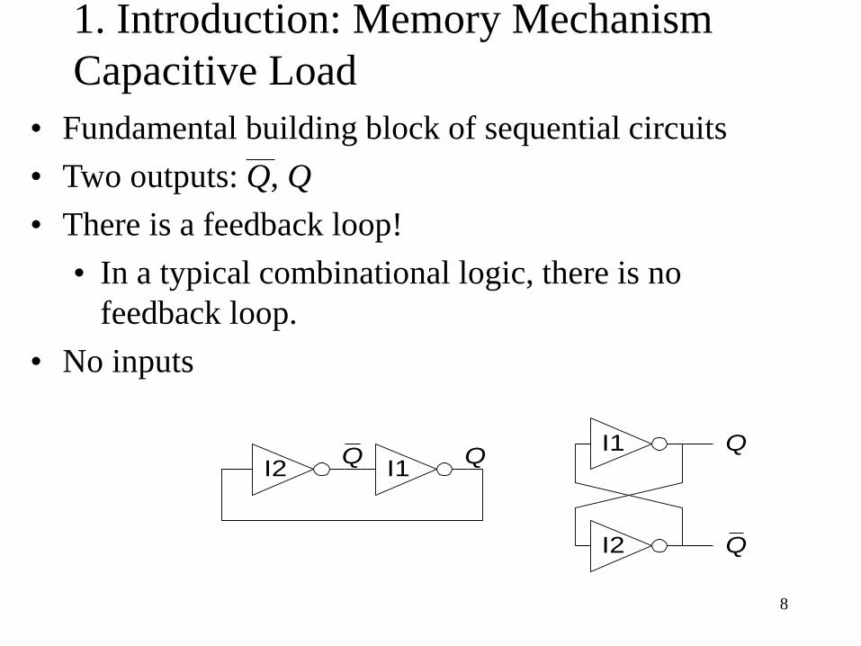
1. Introduction: Memory Mechanism
Capacitive Load
• Fundamental building block of sequential circuits
• Two outputs: Q, Q
• There is a feedback loop!
• In a typical combinational logic, there is no
feedback loop.
• No inputs
QQQ
Q
I1
I2
I2 I1
8
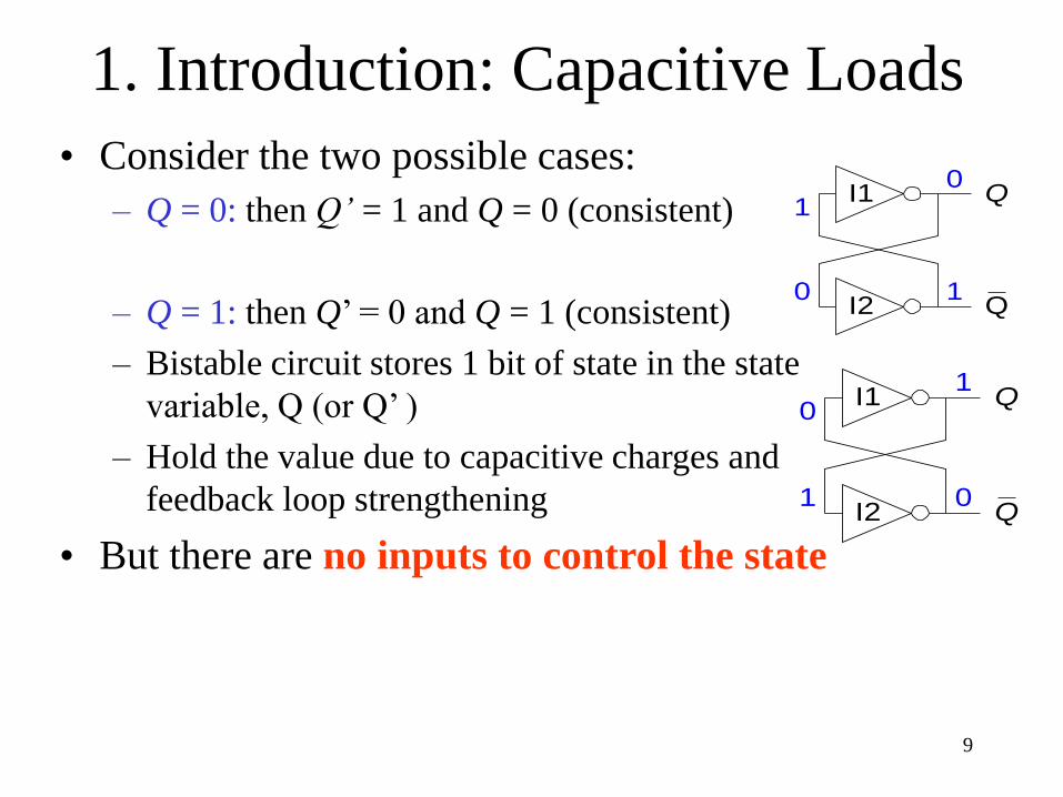
1. Introduction: Capacitive Loads
Q
Q
I1
I2
0
1
1
0
• Consider the two possible cases:
– Q = 0: then Q’ = 1 and Q = 0 (consistent)
– Q = 1: then Q’ = 0 and Q = 1 (consistent)
– Bistable circuit stores 1 bit of state in the state
variable, Q (or Q’ )
– Hold the value due to capacitive charges and
feedback loop strengthening
• But there are no inputs to control the state
Q
Q
I1
I2
1
0
0
1
9

Example
10
Q. Given a memory component made out of a loop
of inverters, the number of inverters in the loop has
to be
A. Even
B. Odd
C. No constraints

1. Introduction: Memory Storage Mechanism
11
• Word line (WL) to
access cell
• Read – measure
voltage difference
between B+ and B-
• Write – force values
of B+ and B- which
may flip the cell
• Static Random
Access Memory -
SRAM
WL
B+ B-
Sense Amp
WriteDriver
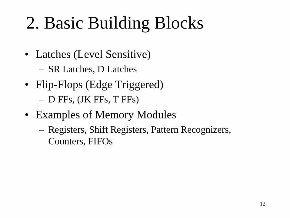
2. Basic Building Blocks
• Latches (Level Sensitive)
– SR Latches, D Latches
• Flip-Flops (Edge Triggered)
– D FFs, (JK FFs, T FFs)
• Examples of Memory Modules
– Registers, Shift Registers, Pattern Recognizers,
Counters, FIFOs
12

2. Basic Building Blocks: Flight attendant call button
• Flight attendant call button
– Press call: light turns on
• Stays on after button released
– Press cancel: light turns off
– Logic gate circuit to implement this?
13
a
BitStorage
Blue lightCallbutton
Cancelbutton
1. Call button pressed – light turns on
BitStorage
Blue lightCallbutton
Cancelbutton
2. Call button released – light stays on
BitStorage
Blue lightCallbutton
Cancelbutton
3. Cancel button pressed – light turns off
• SR latch implementation– Call=1 : sets Q to 1 and keeps it at 1
– Cancel=1 : resets Q to 0
R
S
Q
C all
button
Blue light
Cancelbutton
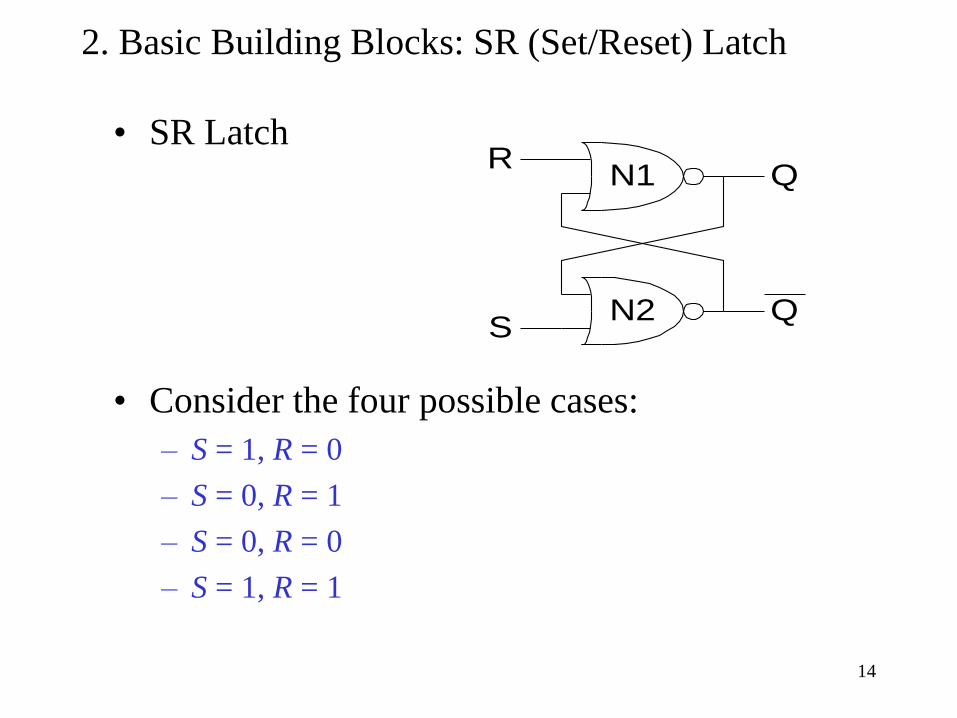
2. Basic Building Blocks: SR (Set/Reset) Latch
R
S
Q
Q
N1
N2
• SR Latch
• Consider the four possible cases:
– S = 1, R = 0
– S = 0, R = 1
– S = 0, R = 0
– S = 1, R = 1
14
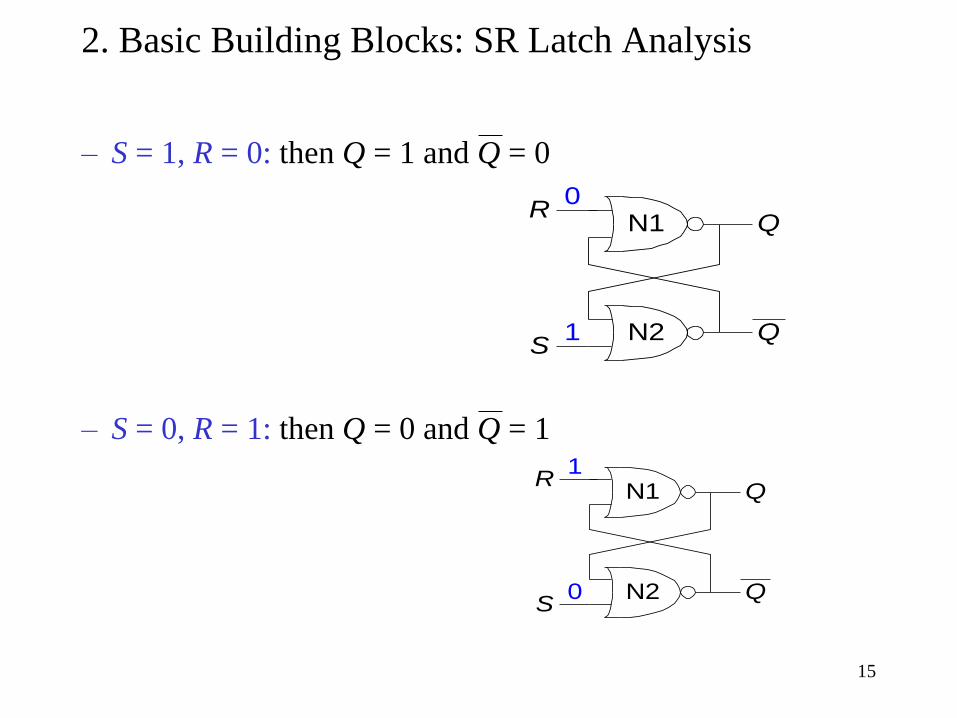
2. Basic Building Blocks: SR Latch Analysis
– S = 1, R = 0: then Q = 1 and Q = 0
– S = 0, R = 1: then Q = 0 and Q = 1
R
S
Q
Q
N1
N2
0
1
R
S
Q
Q
N1
N2
1
0
15
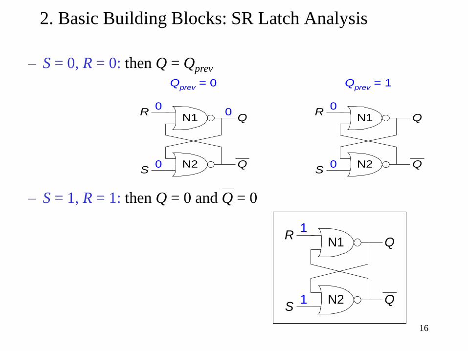
2. Basic Building Blocks: SR Latch Analysis
– S = 0, R = 0: then Q = Qprev
– S = 1, R = 1: then Q = 0 and Q = 0
R
S
Q
Q
N1
N2
1
1
R
S
Q
Q
N1
N2
0
0
R
S
Q
Q
N1
N2
0
0
0
Qprev
= 0 Qprev
= 1
16
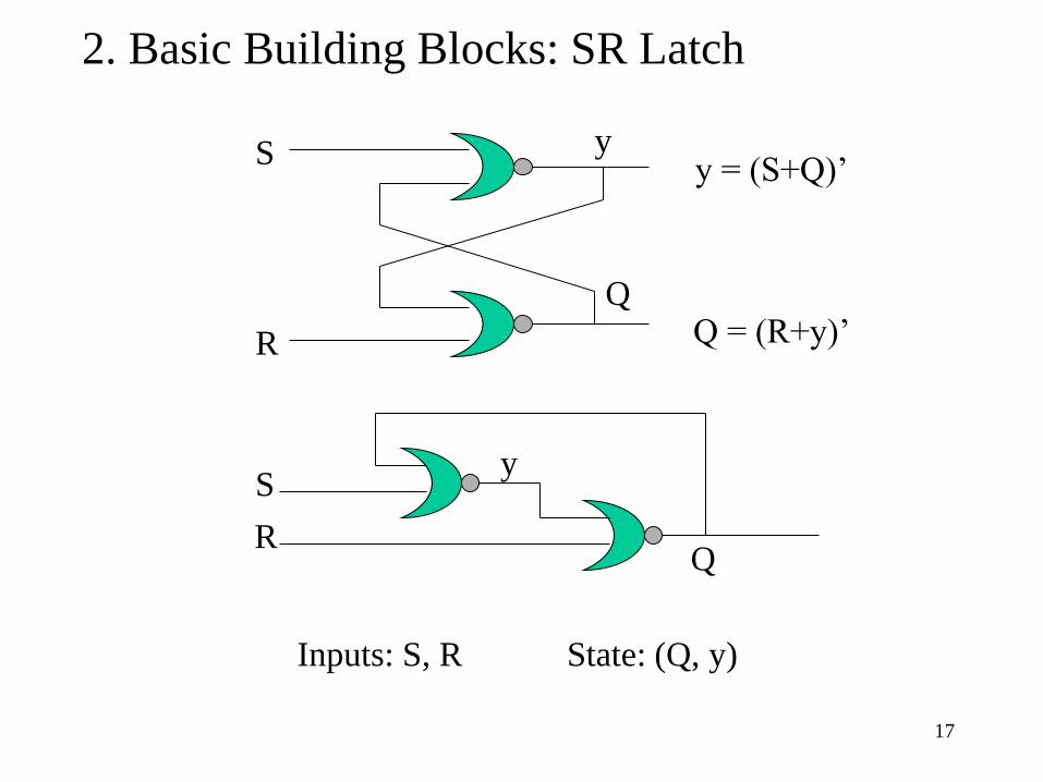
2. Basic Building Blocks: SR Latch
Inputs: S, R State: (Q, y)
S
R
y
Q
17
S
R
y
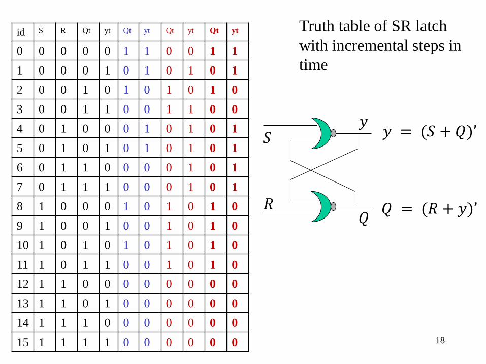
QQ = (R+y)’
y = (S+Q)’
18
𝑆
𝑅
𝑦
𝑄𝑄 = (𝑅 + 𝑦)’
𝑦 = (𝑆 + 𝑄)’
id S R Qt yt Qt yt Qt yt Qt yt
0 0 0 0 0 1 1 0 0 1 1
1 0 0 0 1 0 1 0 1 0 1
2 0 0 1 0 1 0 1 0 1 0
3 0 0 1 1 0 0 1 1 0 0
4 0 1 0 0 0 1 0 1 0 1
5 0 1 0 1 0 1 0 1 0 1
6 0 1 1 0 0 0 0 1 0 1
7 0 1 1 1 0 0 0 1 0 1
8 1 0 0 0 1 0 1 0 1 0
9 1 0 0 1 0 0 1 0 1 0
10 1 0 1 0 1 0 1 0 1 0
11 1 0 1 1 0 0 1 0 1 0
12 1 1 0 0 0 0 0 0 0 0
13 1 1 0 1 0 0 0 0 0 0
14 1 1 1 0 0 0 0 0 0 0
15 1 1 1 1 0 0 0 0 0 0
Truth table of SR latch
with incremental steps in
time

19
“State Table” of SR latch
\SR𝑄𝑦
00 01 10 11
00 11 01 10 00
01 01 01 10 00
10 10 01 10 00
11 00 01 10 00
id S R Qt yt Qt yt Qt yt Qt yt
0 0 0 0 0 1 1 0 0 1 1
1 0 0 0 1 0 1 0 1 0 1
2 0 0 1 0 1 0 1 0 1 0
3 0 0 1 1 0 0 1 1 0 0
4 0 1 0 0 0 1 0 1 0 1
5 0 1 0 1 0 1 0 1 0 1
6 0 1 1 0 0 0 0 1 0 1
7 0 1 1 1 0 0 0 1 0 1
8 1 0 0 0 1 0 1 0 1 0
9 1 0 0 1 0 0 1 0 1 0
10 1 0 1 0 1 0 1 0 1 0
11 1 0 1 1 0 0 1 0 1 0
12 1 1 0 0 0 0 0 0 0 0
13 1 1 0 1 0 0 0 0 0 0
14 1 1 1 0 0 0 0 0 0 0
15 1 1 1 1 0 0 0 0 0 0

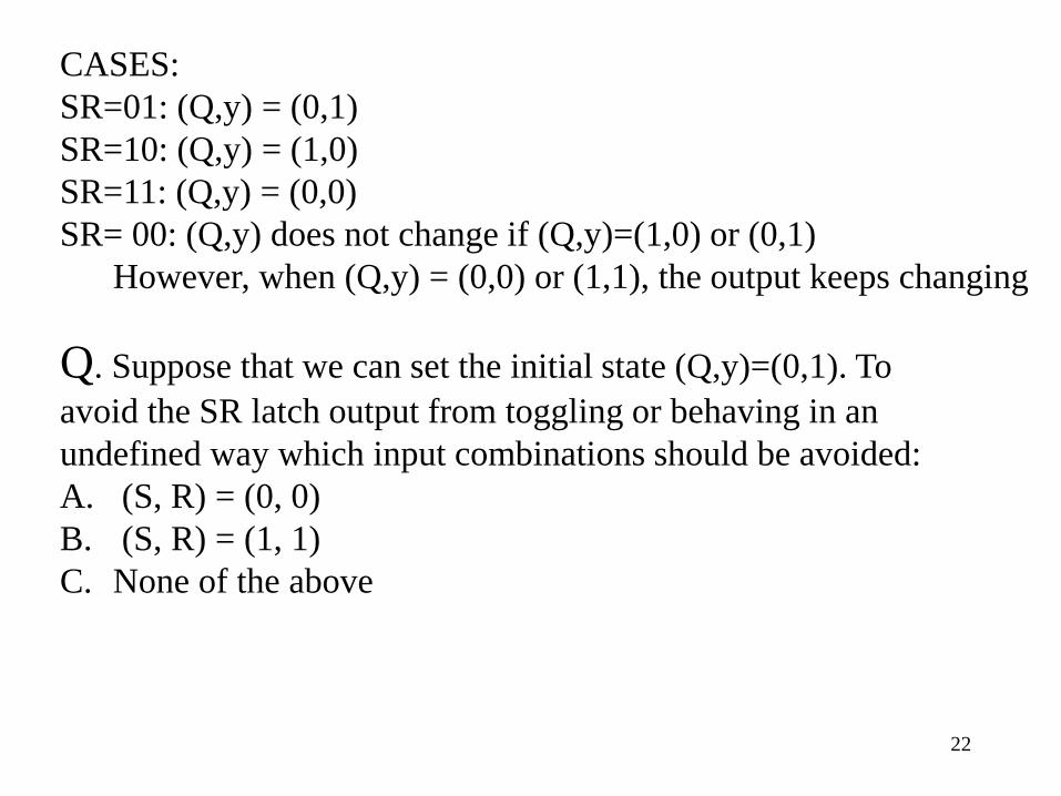
CASES:
SR=01: (Q,y) = (0,1)
SR=10: (Q,y) = (1,0)
SR=11: (Q,y) = (0,0)
SR= 00: (Q,y) does not change if (Q,y)=(1,0) or (0,1)
However, when (Q,y) = (0,0) or (1,1), the output keeps changing
20
Remark: To verify the design, we need to
enumerate all combinations.

21
01
11
00
10
00
10
1001
0000
11
10
01
00
01
11
1011
01
11
Q y
StateSR
Q y
State
TransitionPresent
State
Next
State State diagram
\SR
Qy
00 01 10 11
00 11 01 10 00
01 01 01 10 00
10 10 01 10 00
11 00 01 10 00
State Table and
State Diagram
State Table
CASES:
SR=01: (Q,y) = (0,1)
SR=10: (Q,y) = (1,0)
SR=11: (Q,y) = (0,0)
SR= 00: (Q,y) does not change if (Q,y)=(1,0) or (0,1)
However, when (Q,y) = (0,0) or (1,1), the output keeps changing
22
Q. Suppose that we can set the initial state (Q,y)=(0,1). To
avoid the SR latch output from toggling or behaving in an
undefined way which input combinations should be avoided:
A. (S, R) = (0, 0)
B. (S, R) = (1, 1)
C. None of the above

CASES:
SR=01: (Q,y) = (0,1)
SR=10: (Q,y) = (1,0)
SR=11: (Q,y) = (0,0)
SR= 00: (Q,y) does not change if (Q,y)=(1,0) or (0,1)
However, when (Q,y) = (0,0) or (1,1), the output keeps changing
23
We set the initial state (Q,y)=(0,1) or (1,0). To avoid the state
(Q,y)= (0,0) or (1,1), we block the input SR=11.
Thus, without input SR=11, the state can only be (Q,y)=(0,1)
or (1,0).
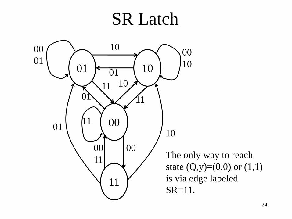
SR Latch
24
01
11
00
10
00
10
1001
0000
11
10
01
00
01
11
101101
11
The only way to reach
state (Q,y)=(0,0) or (1,1)
is via edge labeled
SR=11.

SR Latch
25
01
11
00
10
00
10
1001
0000
11
10
01
00
01
11
101101
11
The only way to reach
state (Q,y)=(0,0) or (1,1)
is via edge labeled
SR=11.
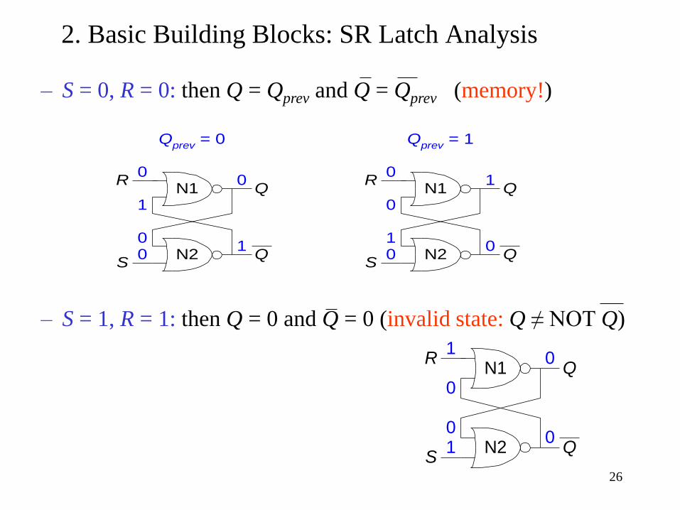
2. Basic Building Blocks: SR Latch Analysis
– S = 0, R = 0: then Q = Qprev and Q = Qprev (memory!)
– S = 1, R = 1: then Q = 0 and Q = 0 (invalid state: Q ≠ NOT Q)
R
S
Q
Q
N1
N2
1
1
0
00
0
R
S
Q
Q
N1
N2
0
0
1
01
0
R
S
Q
Q
N1
N2
0
0
0
10
1
Qprev
= 0 Qprev
= 1
26
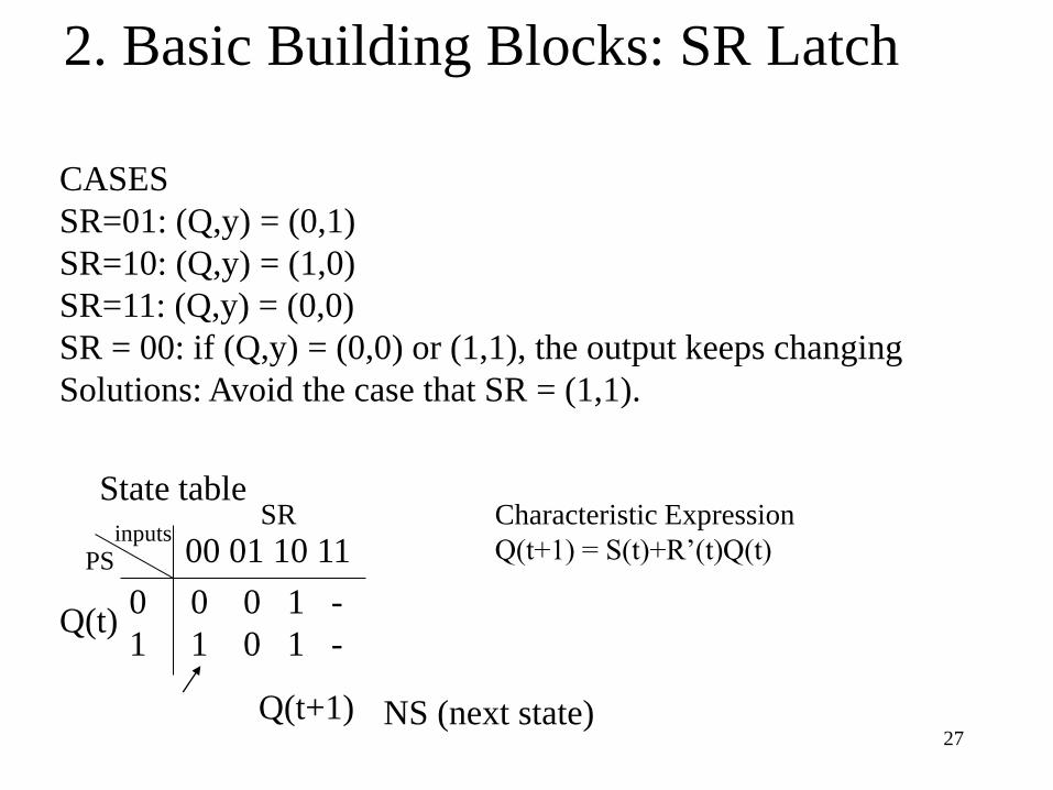
CASES
SR=01: (Q,y) = (0,1)
SR=10: (Q,y) = (1,0)
SR=11: (Q,y) = (0,0)
SR = 00: if (Q,y) = (0,0) or (1,1), the output keeps changing
Solutions: Avoid the case that SR = (1,1).
Characteristic Expression
Q(t+1) = S(t)+R’(t)Q(t)
Q(t+1) NS (next state)
0 0 0 1 -
1 1 0 1 -
PSinputs
00 01 10 11
State tableSR
Q(t)
27
2. Basic Building Blocks: SR Latch
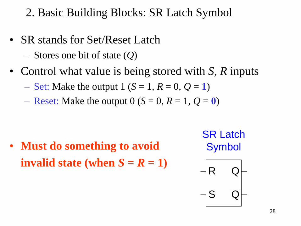
2. Basic Building Blocks: SR Latch Symbol
• SR stands for Set/Reset Latch
– Stores one bit of state (Q)
• Control what value is being stored with S, R inputs
– Set: Make the output 1 (S = 1, R = 0, Q = 1)
– Reset: Make the output 0 (S = 0, R = 1, Q = 0)
• Must do something to avoid
invalid state (when S = R = 1)
S
R Q
Q
SR Latch
Symbol
28

2. Basic Building Blocks: D Latch
D Latch
Symbol
CLK
D Q
Q
• Two inputs: CLK, D
– CLK: controls when the output changes
– D (the data input): controls what the
output changes to
• Function
– When CLK = 1, D passes through to Q
(the latch is transparent)
– When CLK = 0, Q holds its previous
value (the latch is opaque)
• Avoids invalid case when Q ≠ NOT Q
29

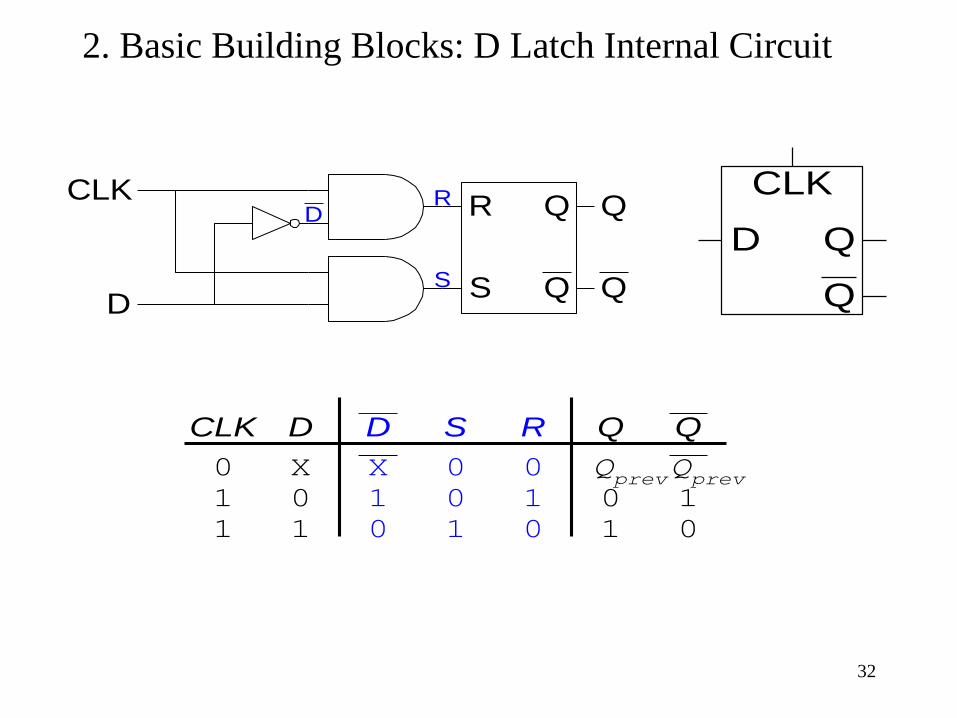
2. Basic Building Blocks: D Latch Internal Circuit
CLK
D Q
Q
30
S
R Q
Q
SR Latch
Symbol

2. Basic Building Blocks: D Latch Internal Circuit
S
R Q
Q
Q
QD
CLKD
R
S
CLK
D Q
Q
S R Q QCLK D
0 X
1 0
1 1
D
31
2. Basic Building Blocks: D Latch Internal Circuit
S
R Q
Q
Q
QD
CLKD
R
S
CLK
D Q
Q
S R Q
0 0 Qprev
0 1 0
1 0 1
Q
1
0
CLK D
0 X
1 0
1 1
D
X
1
0
Qprev
32

2. Basic Building Blocks: D Flip-Flop
• Two inputs: CLK, D
• Function
– The flip-flop “samples” D on the rising
edge of CLK
• When CLK rises from 0 to 1, D
passes through to Q
• Otherwise, Q holds its previous value
– Q changes only on the rising edge of
CLK
• A flip-flop is called an edge-triggered device
because it is activated on the clock edge
D Flip-Flop
Symbols
D Q
Q
33

2. Basic Building Blocks: D FF Internal Circuit
CLK
D Q
Q
CLK
D Q
Q
Q
Q
DN1
CLK
L1 L2
34

D Flip-Flop Internal Circuit
CLK
D Q
Q
CLK
D Q
Q
Q
Q
DN1
CLK
L1 L2
• Two back-to-back latches (L1 and L2) controlled by
complementary clocks
• When CLK = 0
– L1 is transparent, L2 is opaque
– D passes through to N1
• When CLK = 1
– L2 is transparent, L1 is opaque
– N1 passes through to Q
• Thus, on the edge of the clock (when CLK rises from 0 1)
– D passes through to Q
CLK
D Q
Q
CLK
D Q
Q
Q
Q
DN1
CLK
L1 L2
35

D Flip-Flop vs. D Latch
CLK
D Q
Q
D Q
Q
CLK
D
Q (latch)
Q (flop)
36

D Flip-Flop vs. D Latch
CLK
D Q
Q
D Q
Q
CLK
D
Q (latch)
Q (flop)
37
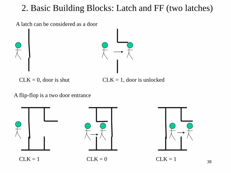
2. Basic Building Blocks: Latch and FF (two latches)
A latch can be considered as a door
CLK = 0, door is shut CLK = 1, door is unlocked
A flip-flop is a two door entrance
CLK = 1 CLK = 0 CLK = 138

2. Basic Building Blocks: D Flip-Flop (Delay)
D
CLK
Q
Q’
Id D Q(t) Q(t+1)
0 0 0 0
1 0 1 0
2 1 0 1
3 1 1 1
Characteristic Expression: Q(t+1) = D(t)
0 0 1
1 0 1
PSD
0 1
State table
NS= Q(t+1)
39
CLK
D Q
Q
CLK
D Q
Q
Q
Q
DN1
CLK
L1 L2

2. Basic Building Blocks: Example
40
Can D flip-flip serve as a memory
component?
A.Yes
B.No
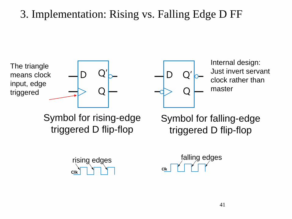
3. Implementation: Rising vs. Falling Edge D FF
41
D Q’
Q
Q’D
Q
Symbol for rising-edge
triggered D flip-flopSymbol for falling-edge
triggered D flip-flop
Clk
rising edgesClk
falling edges
Internal design:
Just invert servant
clock rather than
master
The triangle
means clock
input, edge
triggered
Internal
Circuit
D Q
CLKEN
DQ
0
1D Q
EN
Symbol
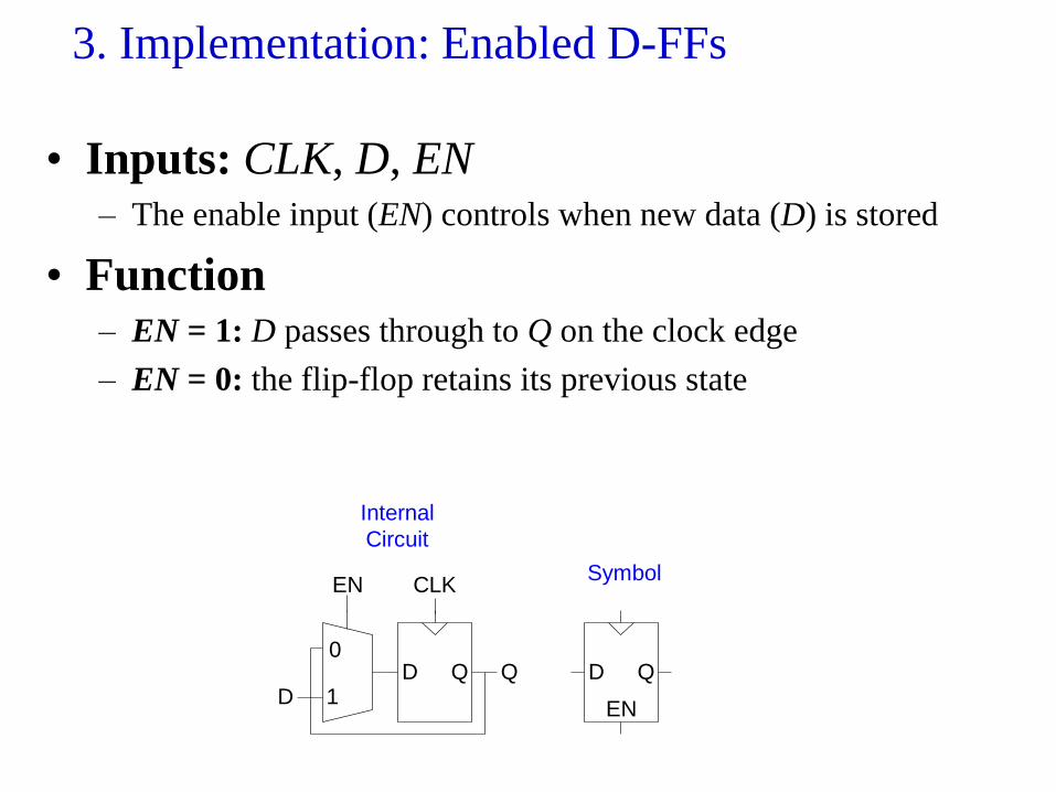
• Inputs: CLK, D, EN– The enable input (EN) controls when new data (D) is stored
• Function– EN = 1: D passes through to Q on the clock edge
– EN = 0: the flip-flop retains its previous state
3. Implementation: Enabled D-FFs

43
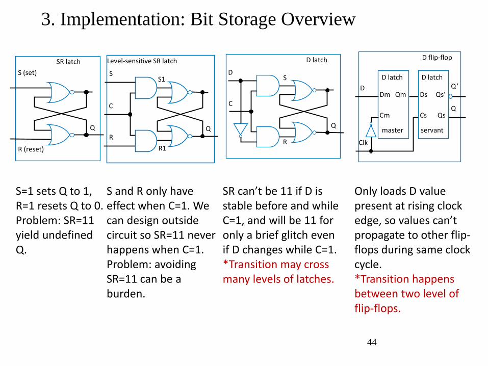
3. Implementation: Bit Storage Overview
44
S
R
D
Q
C
D latch
Only loads D value present at rising clock edge, so values can’t propagate to other flip-flops during same clock cycle.*Transition happens between two level of flip-flops.
SR can’t be 11 if D is stable before and while C=1, and will be 11 for only a brief glitch even if D changes while C=1.*Transition may cross many levels of latches.
S1
R1
S
Q
C
R
Level-sensitive SR latch
S and R only have effect when C=1. We can design outside circuit so SR=11 never happens when C=1. Problem: avoiding SR=11 can be a burden.
R (reset)
S (set)
Q
SR latch
S=1 sets Q to 1, R=1 resets Q to 0. Problem: SR=11 yield undefined Q.
D flip-flop
D latch
master
D latch
servant
Dm Qm
Cm
DsD
Clk
Qs’
Cs Qs
Q ’
Q

45

3. Implementation: Shift register• Holds & shifts samples of input
46
D Q D Q D Q D QIN
OUT1 OUT2 OUT3 OUT4
CLK
Time Input OUT1 OUT2 OUT3 OUT4
0 1 0 0 0 0
1 0
2 1
3 1
4 0
5 0
6 0
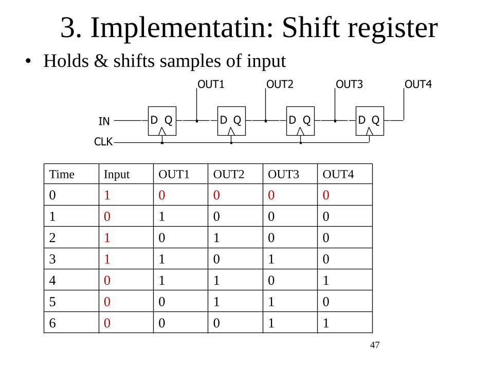
3. Implementatin: Shift register• Holds & shifts samples of input
47
D Q D Q D Q D QIN
OUT1 OUT2 OUT3 OUT4
CLK
Time Input OUT1 OUT2 OUT3 OUT4
0 1 0 0 0 0
1 0 1 0 0 0
2 1 0 1 0 0
3 1 1 0 1 0
4 0 1 1 0 1
5 0 0 1 1 0
6 0 0 0 1 1
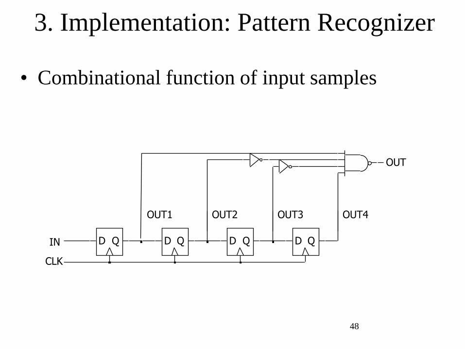
3. Implementation: Pattern Recognizer
• Combinational function of input samples
48
D Q D Q D Q D QIN
OUT1 OUT2 OUT3 OUT4
CLK
OUT

3. Implementation: Counters
49
D Q D Q D Q D QIN
OUT1 OUT2 OUT3 OUT4
CLK
•Sequences through a fixed set of patterns

Appendix: slides on BSV
Describing Sequential Ckts
• State diagrams and next-state tables nor are
suitable for describing very large digital designs
– large circuits must be described in a modular
fashion -- as a collection of cooperating FSMs
• BSV is a modern programming language to
describe cooperating FSMs
– We will give various examples of FSMs in
BSV
CSE 140L
W2017L04-50
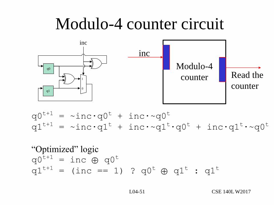
Modulo-4 counter circuit
Modulo-4
counter
inc
Read the
counter
q0t+1 = ~inc∙q0t + inc∙~q0t
q1t+1 = ~inc∙q1t + inc∙~q1t∙q0t + inc∙q1t∙~q0t
“Optimized” logicq0t+1 = inc q0t
q1t+1 = (inc == 1) ? q0t q1t : q1t
q0
inc
1
0q1
CSE 140L W2017L04-51

Modulo-4 counter circuit
q0t+1 = ~inc∙q0t + inc∙~q0t
q1t+1 = ~inc∙q1t + inc∙~q1t∙q0t
+ inc∙q1t∙~q0t
“Optimized” logicq0t+1 =inc q0t
q1t+1 =(inc == 1) ? q0tq1t:q1t
q0
inc
1
0q1
CSE 140L W2017L04-52
PS\input inc=0 inc=1
00 00 01
01 01 10
10 10 11
11 11 00
PS: q1t q0t, NS: q1t+1 q0t+1
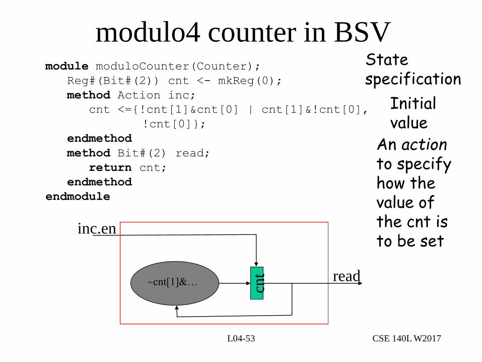
modulo4 counter in BSVmodule moduloCounter(Counter);
Reg#(Bit#(2)) cnt <- mkReg(0);
method Action inc;
cnt <={!cnt[1]&cnt[0] | cnt[1]&!cnt[0],
!cnt[0]};
endmethod
method Bit#(2) read;
return cnt;
endmethod
endmodule
~cnt[1]&…
inc.en
readcn
t
An actionto specify how the value of the cnt is to be set
State specification
CSE 140L W2017L04-53
Initial value

Interface
• Modulo counter has the following interface, i.e., type
• An interface can have many different implementations
– For example, the numbers may be represented as Gray code
interface Counter;
method Action inc;
method Bit#(2) read;
endinterface
CSE 140L W2017L04-54

Modules
• A module in BSV is like a class definition in Java
or C++
– It has internal state
– The internal state can only be read and
manipulated by the (interface) methods
– An action specifies which state elements are to
be modified
– Actions are atomic -- either all the specified
state elements are modified or none of them are
modified (no partially modified state is visible)
CSE 140L W2017L04-55

FIFO Interfaceinterface Fifo#(numeric type size,
type t);
method Bool notFull;
method Bool notEmpty;
method Action enq(t x);
method Action deq;
method t first;
endinterface
xen
en
enq
deq
Fif
o
module
!full
!em
tyfi
rst
notFull
notEmpty
first
- enq should be called only if notFull
returns True;
- deq and first should be called only if
notEmpty returns True
CSE 140L W2017L04-56

module mkCFFifo (Fifo#(1, t));
Reg#(t) d <- mkRegU;
Reg#(Bool) v <- mkReg(False);
method Bool notFull;
return !v;
endmethod
method Bool notEmpty;
return v;
endmethod
method Action enq(t x);
v <= True; d <= x;
endmethod
method Action deq;
v <= False;
endmethod
method t first;
return d;
endmethod
endmodule
One-Element FIFO Implementation
xen
en
enq
deq
Fif
o
module
!full
!em
tyfi
rst
notFull
notEmpty
first
CSE 140L W2017L04-57

FIFO Module:
methods with guarded interfaces
• Every method has a guard (rdy wire); the value returned by a value
method is meaningful only if its guard is true
• Every action method has an enable signal (en wire); an action method is
invoked (en is set to true) only if the guard is true
• Guards make it possible to transfer the responsibility of the correct use of
a method from the user to the compiler
• Guards are extraordinarily convenient for programming and also enhance
modularity of the code
not full
not empty
not empty
n
n
rdy
enab
rdy
enab
rdyen
qd
eqfi
rst
FIFO
interface Fifo#(numeric type size,
type t);
method Action enq(t x);
method Action deq;
method t first;
endinterface
CSE 140L W2017L04-58
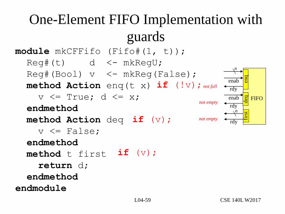
module mkCFFifo (Fifo#(1, t));
Reg#(t) d <- mkRegU;
Reg#(Bool) v <- mkReg(False);
method Action enq(t x)
v <= True; d <= x;
endmethod
method Action deq
v <= False;
endmethod
method t first
return d;
endmethod
endmodule
One-Element FIFO Implementation with
guards
not full
not empty
not empty
n
n
rdy
enab
rdy
enab
rdy
enq
deq
firs
t
FIFO
CSE 140L W2017L04-59
if (!v);
if (v);
if (v);
Related Documents


