ECEN 4517 1 Lecture 6 ECEN 4517/5517 Step-up dc-dc converter with isolation (flyback) Feedback controller to regulate HVDC Experiment 4: inverter system DC-AC inverter (H-bridge) 12 VDC HVDC: 120 - 200 VDC AC load 120 Vrms 60 Hz Battery DC-AC inverter H-bridge DC-DC converter Isolated flyback + – d(t) Feedback controller V ref Digital controller d(t) + v ac (t) –

Welcome message from author
This document is posted to help you gain knowledge. Please leave a comment to let me know what you think about it! Share it to your friends and learn new things together.
Transcript
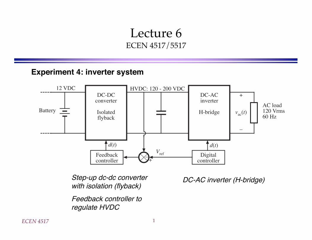
ECEN 4517 1
Lecture 6ECEN 4517/5517
Step-up dc-dc converterwith isolation (flyback)
Feedback controller toregulate HVDC
Experiment 4: inverter system
DC-AC inverter (H-bridge)
12 VDC HVDC: 120 - 200 VDC
AC load120 Vrms60 Hz
Battery
DC-ACinverter
H-bridge
DC-DCconverter
Isolatedflyback
+–
d(t)
Feedbackcontroller
Vref Digitalcontroller
d(t)
+
vac(t)
–

ECEN 4517 2
Due dates
Right now:Prelab assignment for Exp. 3 Part 3 (one from every student)Due within five minutes of beginning of lecture
This week in lab (Feb. 19-21):Nothing due. Try to finish Exp. 3.
Next week in lecture (Feb. 26):Prelab assignment for Exp. 4 Part 1 (one from every student)
Next week in lab (Feb. 26-28):Definitely finish Exp. 3, and begin Exp. 4
The following week in lab (Mar. 4-6):Exp. 3 final report due
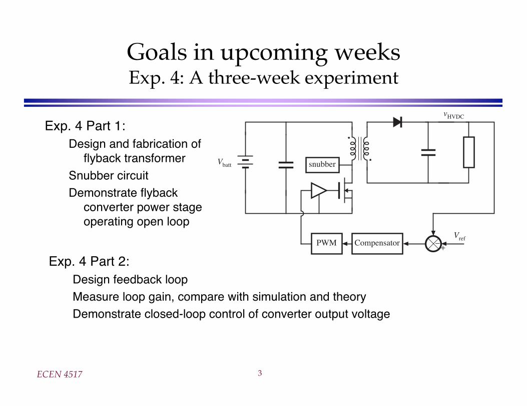
ECEN 4517 3
Goals in upcoming weeksExp. 4: A three-week experiment
Exp. 4 Part 1:Design and fabrication offlyback transformer
Snubber circuitDemonstrate flyback
converter power stageoperating open loop
Exp. 4 Part 2:Design feedback loopMeasure loop gain, compare with simulation and theoryDemonstrate closed-loop control of converter output voltage
snubber
PWM Compensator +– Vref
Vbatt
vHVDC
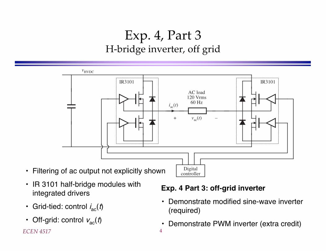
ECEN 4517 4
Exp. 4, Part 3H-bridge inverter, off grid
IR3101 IR3101
vHVDC
AC load120 Vrms
60 Hz
+ vac(t) –
Digitalcontroller
iac(t)
• Filtering of ac output not explicitly shown
• IR 3101 half-bridge modules withintegrated drivers
• Grid-tied: control iac(t)
• Off-grid: control vac(t)
Exp. 4 Part 3: off-grid inverter
• Demonstrate modified sine-wave inverter(required)
• Demonstrate PWM inverter (extra credit)
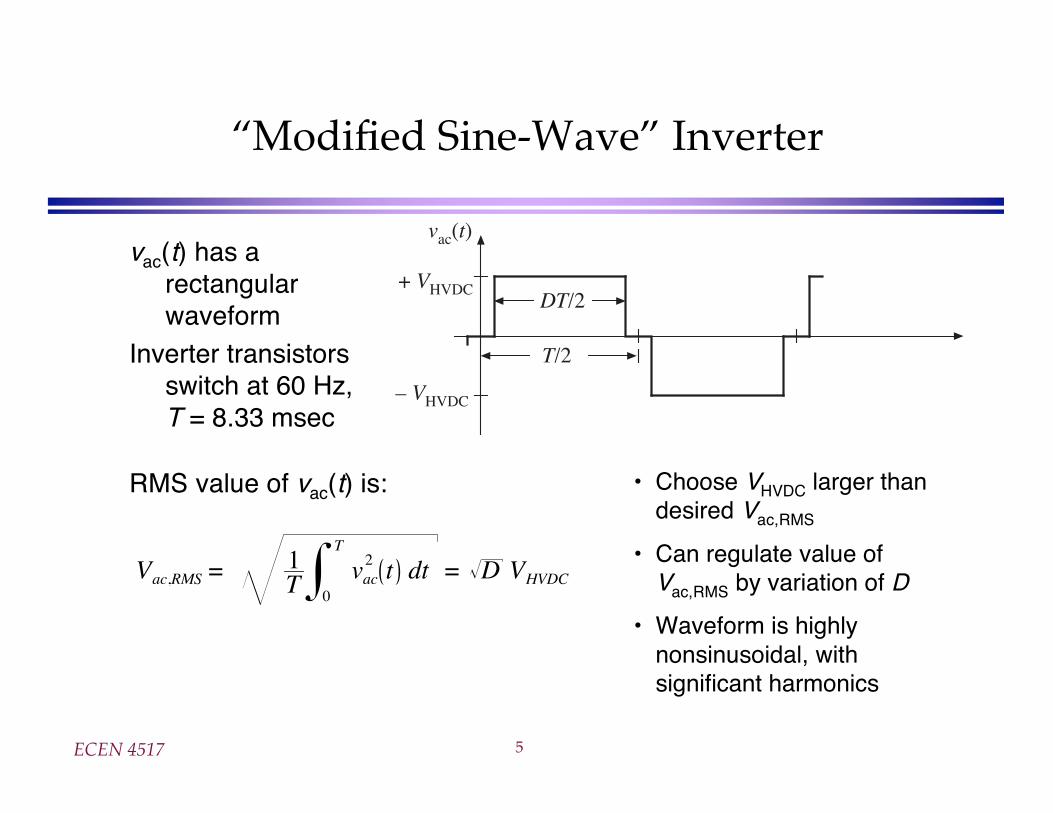
ECEN 4517 5
“Modified Sine-Wave” Inverter
vac(t) has arectangularwaveform
Inverter transistorsswitch at 60 Hz,T = 8.33 msec
T/2
DT/2+ VHVDC
– VHVDC
vac(t)
RMS value of vac(t) is:
Vac,RMS = 1T vac
2 t dt0
T
= D VHVDC
• Choose VHVDC larger thandesired Vac,RMS
• Can regulate value ofVac,RMS by variation of D
• Waveform is highlynonsinusoidal, withsignificant harmonics
ECEN 4517 6
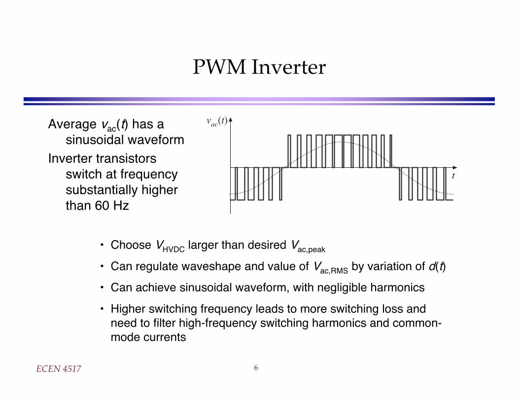
PWM Inverter
Average vac(t) has asinusoidal waveform
Inverter transistorsswitch at frequencysubstantially higherthan 60 Hz
• Choose VHVDC larger than desired Vac,peak
• Can regulate waveshape and value of Vac,RMS by variation of d(t)
• Can achieve sinusoidal waveform, with negligible harmonics
• Higher switching frequency leads to more switching loss andneed to filter high-frequency switching harmonics and common-mode currents
t
vac(t)
ECEN 4517 7
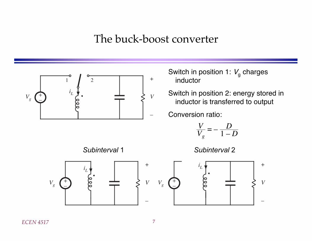
The buck-boost converter
Subinterval 1 Subinterval 2
+–
+
V
–
Vg
iL
+–
+
V
–
Vg
iL
+–
+
V
–
1 2
Vg
iL
VVg
= – D1 – D
Switch in position 1: Vg chargesinductor
Switch in position 2: energy stored ininductor is transferred to output
Conversion ratio:
ECEN 4517 8
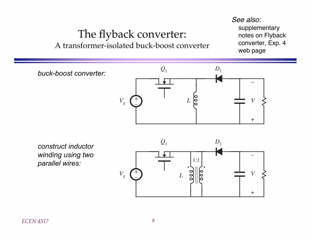
The flyback converter:A transformer-isolated buck-boost converter
buck-boost converter:
construct inductor
winding using two
parallel wires:
+– L
–
V
+
Vg
Q1 D1
+– L
–
V
+
Vg
Q1 D1
1:1
See also:supplementarynotes on Flybackconverter, Exp. 4web page
ECEN 4517 9
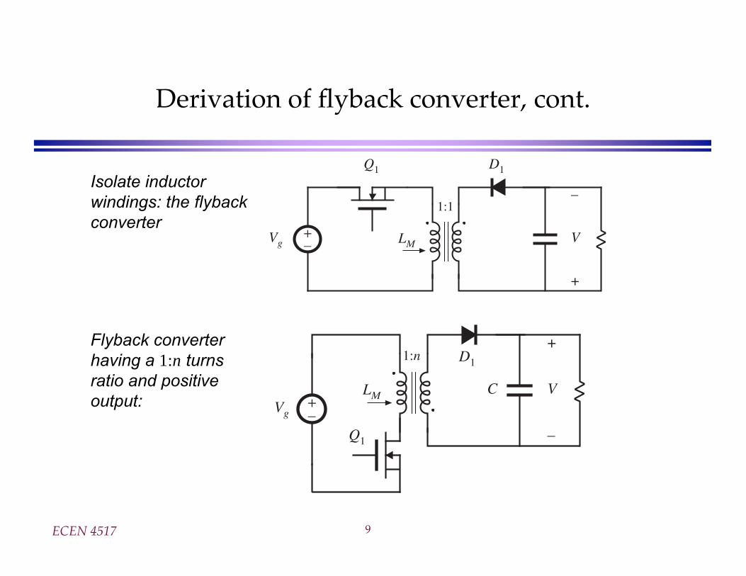
Derivation of flyback converter, cont.
Isolate inductor
windings: the flyback
converter
Flyback converter
having a 1:n turns
ratio and positive
output:
+– LM
–
V
+
Vg
Q1 D1
1:1
+–
LM
+
V
–
Vg
Q1
D11:n
C
ECEN 4517 10
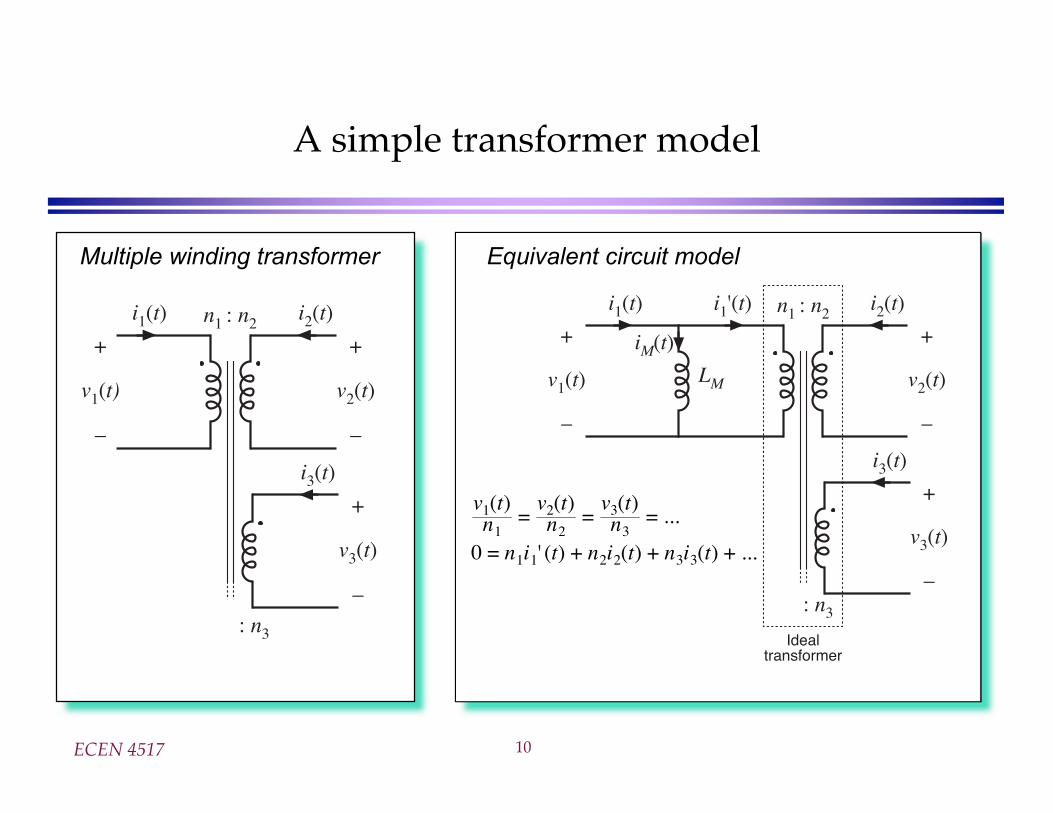
A simple transformer model
Multiple winding transformer Equivalent circuit model
n1 : n2
: n3
+
v1(t)
–
+
v2(t)
–
+
v3(t)
–
i1(t) i2(t)
i3(t)
n1 : n2
: n3
+
v1(t)
–
+
v2(t)
–
+
v3(t)
–
i1(t) i2(t)
i3(t)
Idealtransformer
i1'(t)
LM
iM(t)
v1(t)n1
=v2(t)n2
=v3(t)n3
= ...
0 = n1i1' (t) + n2i2(t) + n3i3(t) + ...
ECEN 4517 11
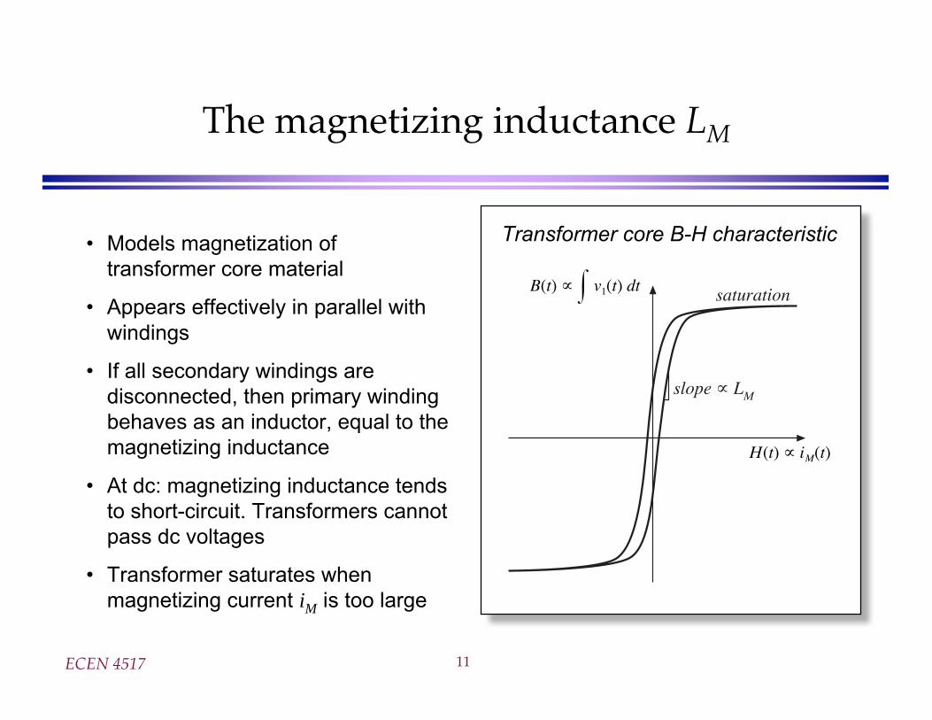
The magnetizing inductance LM
Transformer core B-H characteristic• Models magnetization of
transformer core material
• Appears effectively in parallel with
windings
• If all secondary windings are
disconnected, then primary winding
behaves as an inductor, equal to the
magnetizing inductance
• At dc: magnetizing inductance tends
to short-circuit. Transformers cannot
pass dc voltages
• Transformer saturates when
magnetizing current iM
is too large
B(t) ∝ v1(t) dt
H(t) ∝ iM(t)
slope ∝ LM
saturation
ECEN 4517 12
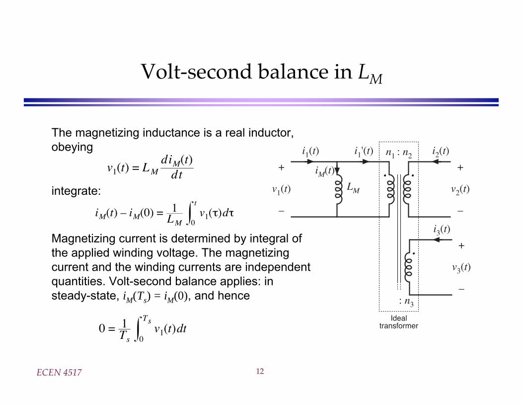
Volt-second balance in LM
The magnetizing inductance is a real inductor,
obeying
integrate:
Magnetizing current is determined by integral of
the applied winding voltage. The magnetizing
current and the winding currents are independent
quantities. Volt-second balance applies: in
steady-state, iM
(Ts) = i
M(0), and hence
n1 : n2
: n3
+
v1(t)
–
+
v2(t)
–
+
v3(t)
–
i1(t) i2(t)
i3(t)
Idealtransformer
i1'(t)
LM
iM(t)v1(t) = L MdiM(t)
dt
iM(t) – iM(0) = 1L M
v1(τ)dτ0
t
0 = 1Ts
v1(t)dt0
Ts
ECEN 4517 13
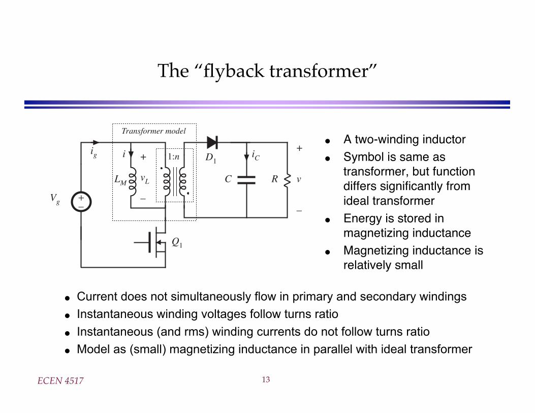
The “flyback transformer”
A two-winding inductorSymbol is same astransformer, but functiondiffers significantly fromideal transformerEnergy is stored inmagnetizing inductanceMagnetizing inductance isrelatively small
Current does not simultaneously flow in primary and secondary windings
Instantaneous winding voltages follow turns ratio
Instantaneous (and rms) winding currents do not follow turns ratio
Model as (small) magnetizing inductance in parallel with ideal transformer
+–
LM
+
v
–Vg
Q1
D11:n
C
Transformer model
iig
R
iC+
vL
–
ECEN 4517 14
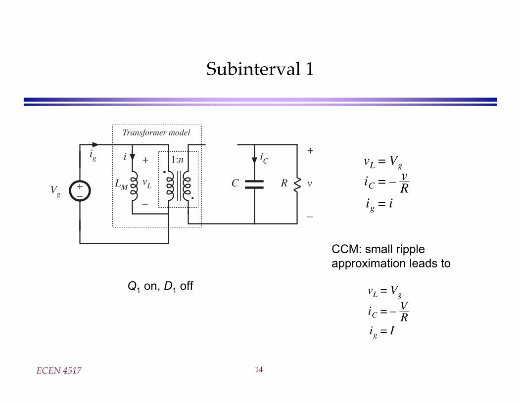
Subinterval 1
CCM: small ripple
approximation leads to
+–
LM
+
v
–
Vg
1:n
C
Transformer model
iig
R
iC+
vL
–
vL = Vg
iC = – vR
ig = i
vL = Vg
iC = – VR
ig = I
Q1 on, D1 off
ECEN 4517 15
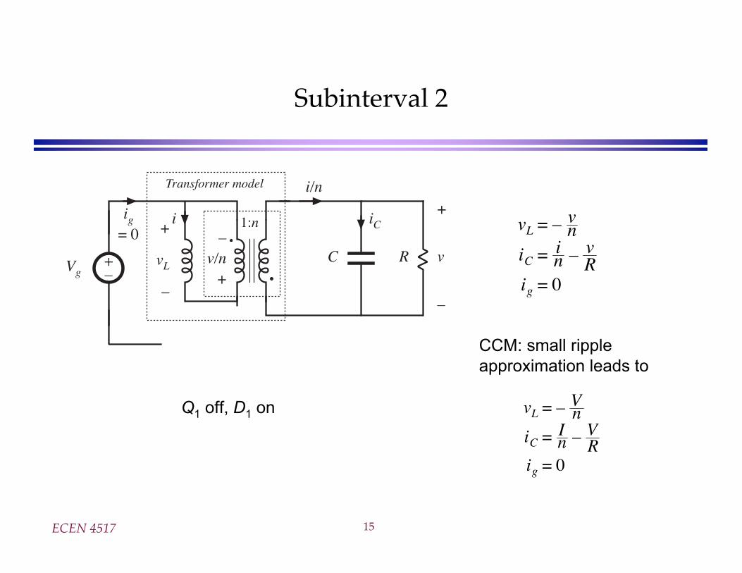
Subinterval 2
CCM: small ripple
approximation leads to
vL = – vn
iC = in – v
Rig = 0
vL = – Vn
iC = In – V
Rig = 0
+–
+
v
–
Vg
1:n
C
Transformer model
i
R
iC
i/n
–v/n
+
+
vL
–
ig= 0
Q1 off, D1 on
ECEN 4517 16
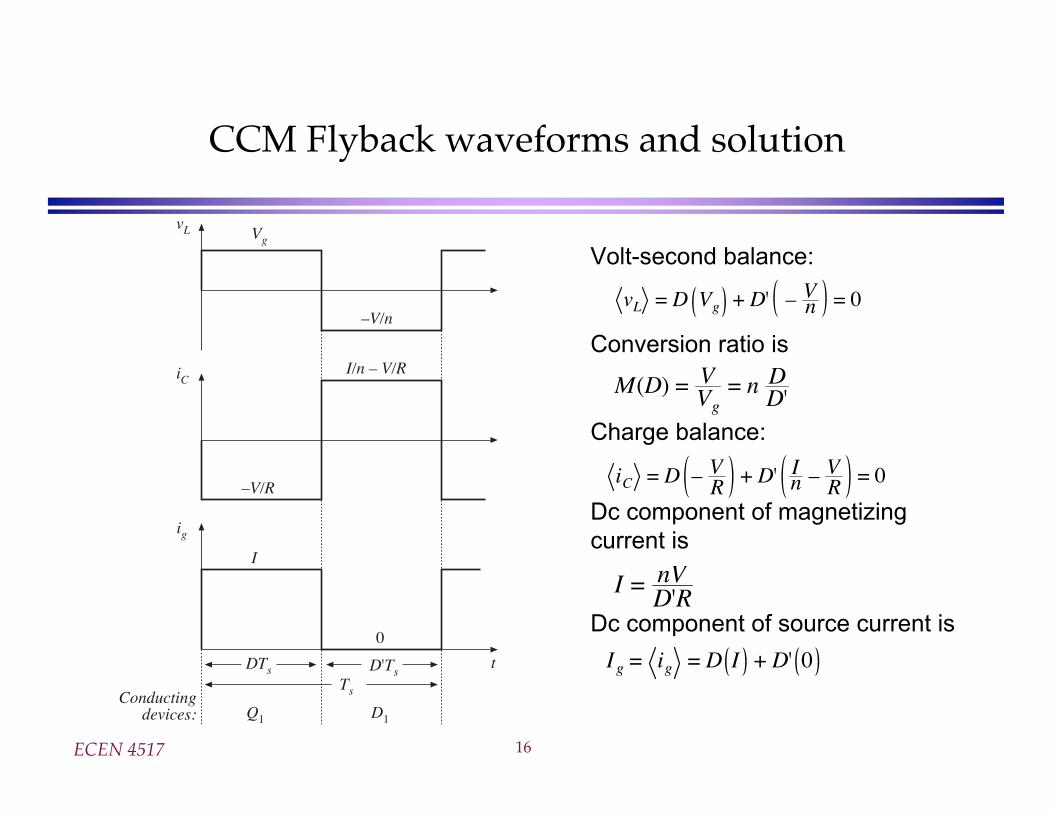
CCM Flyback waveforms and solution
Volt-second balance:
Conversion ratio is
Charge balance:
Dc component of magnetizing
current is
Dc component of source current is
vL
iC
ig
t
Vg
0
DTs D'TsTs
Q1 D1
Conductingdevices:
–V/n
–V/R
I/n – V/R
I
vL = D Vg + D' – Vn = 0
M(D) = VVg
= n DD'
iC = D – VR + D' I
n – VR = 0
I = nVD'R
Ig = ig = D I + D' 0
ECEN 4517 17
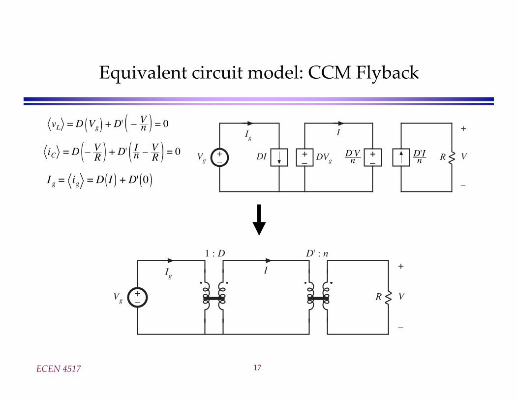
Equivalent circuit model: CCM Flyback
+–
+– R
+
V
–
VgD'In
D'Vn
+–
DVgDI
IIg
+– R
+
V
–
Vg
IIg
1 : D D' : n
vL = D Vg + D' – Vn = 0
iC = D – VR + D' I
n – VR = 0
Ig = ig = D I + D' 0
ECEN 4517 18
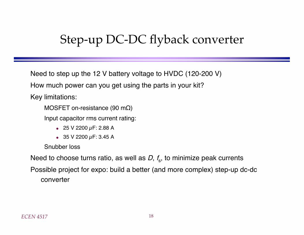
Step-up DC-DC flyback converter
Need to step up the 12 V battery voltage to HVDC (120-200 V)
How much power can you get using the parts in your kit?
Key limitations:
MOSFET on-resistance (90 m )
Input capacitor rms current rating:
25 V 2200 μF: 2.88 A
35 V 2200 μF: 3.45 A
Snubber loss
Need to choose turns ratio, as well as D, fs, to minimize peak currents
Possible project for expo: build a better (and more complex) step-up dc-dcconverter
ECEN 4517 19
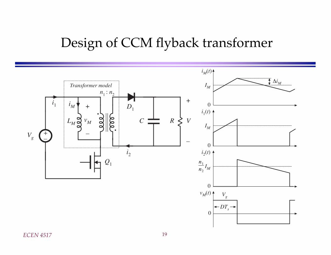
Design of CCM flyback transformer
+–
LM
+
V
–Vg
Q1
D1
n1 : n2
C
Transformer model
iMi1
R
+
vM
–
i2
vM(t)
0
Vg
DTs
iM(t)
IM
0
ΔiM
i1(t)
IM
0i2(t)
IM
0
n1
n2
ECEN 4517 20
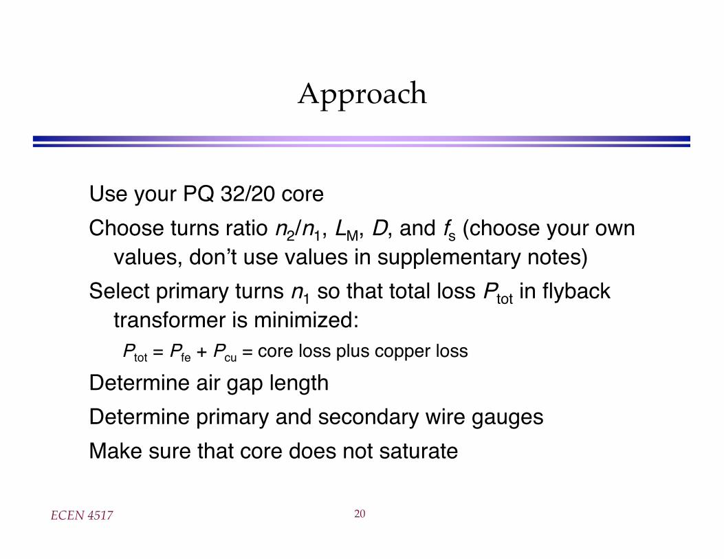
Approach
Use your PQ 32/20 core
Choose turns ratio n2/n1, LM, D, and fs (choose your ownvalues, don t use values in supplementary notes)
Select primary turns n1 so that total loss Ptot in flybacktransformer is minimized:Ptot = Pfe + Pcu = core loss plus copper loss
Determine air gap length
Determine primary and secondary wire gauges
Make sure that core does not saturate
ECEN 4517 21
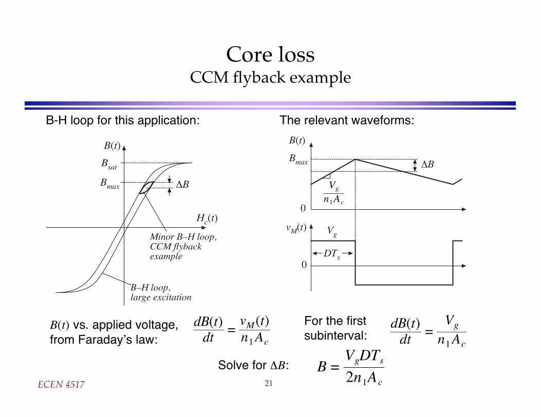
Core lossCCM flyback example
dB(t)dt
=vM (t)n1Ac
dB(t)dt
=Vg
n1Ac
B(t)
Hc(t)
Minor B–H loop,CCM flybackexample
B–H loop,large excitation
Bsat
ΔBBmax
vM(t)
0
Vg
DTs
B(t)
Bmax
0
ΔB
Vg
n1Ac
B-H loop for this application: The relevant waveforms:
B(t) vs. applied voltage,from Faraday s law:
For the firstsubinterval:
Solve for B: �B =VgDTs2n1Ac
ECEN 4517 22
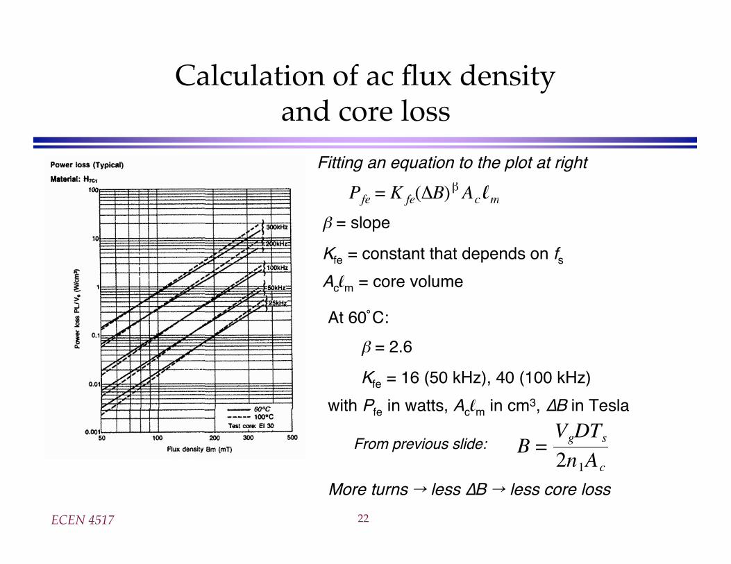
Calculation of ac flux densityand core loss
�B =VgDTs2n1Ac
Pfe = K fe(ΔB)β Ac lm
= slope
Kfe = constant that depends on fsAclm = core volume
Fitting an equation to the plot at right
At 60˚C:
= 2.6
Kfe = 16 (50 kHz), 40 (100 kHz)
with Pfe in watts, Aclm in cm3, B in Tesla
More turns less B less core loss
From previous slide:
ECEN 4517 23
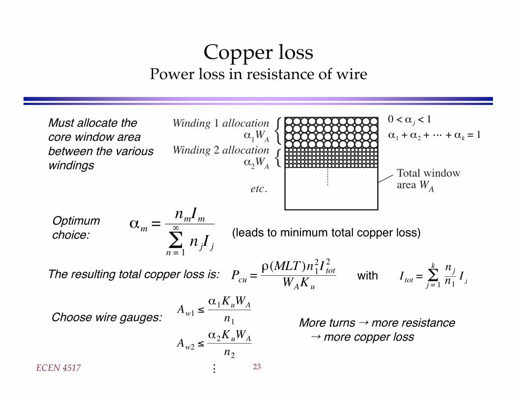
Copper lossPower loss in resistance of wire
Total windowarea WA
Winding 1 allocationα1WA
Winding 2 allocationα2WA
etc.
{{
0 < α j < 1
α1 + α2 + + αk = 1Must allocate thecore window areabetween the variouswindings
αm =nmIm
n jI jΣn = 1
∞Optimumchoice: (leads to minimum total copper loss)
The resulting total copper loss is: Pcu =ρ(MLT )n1
2I tot2
WAK uI tot =
n jn1
I jΣj = 1
k
with
Aw1 ≤α1KuWA
n1
Aw2 ≤α2K uWA
n2
Choose wire gauges: More turns more resistance more copper loss
ECEN 4517 24
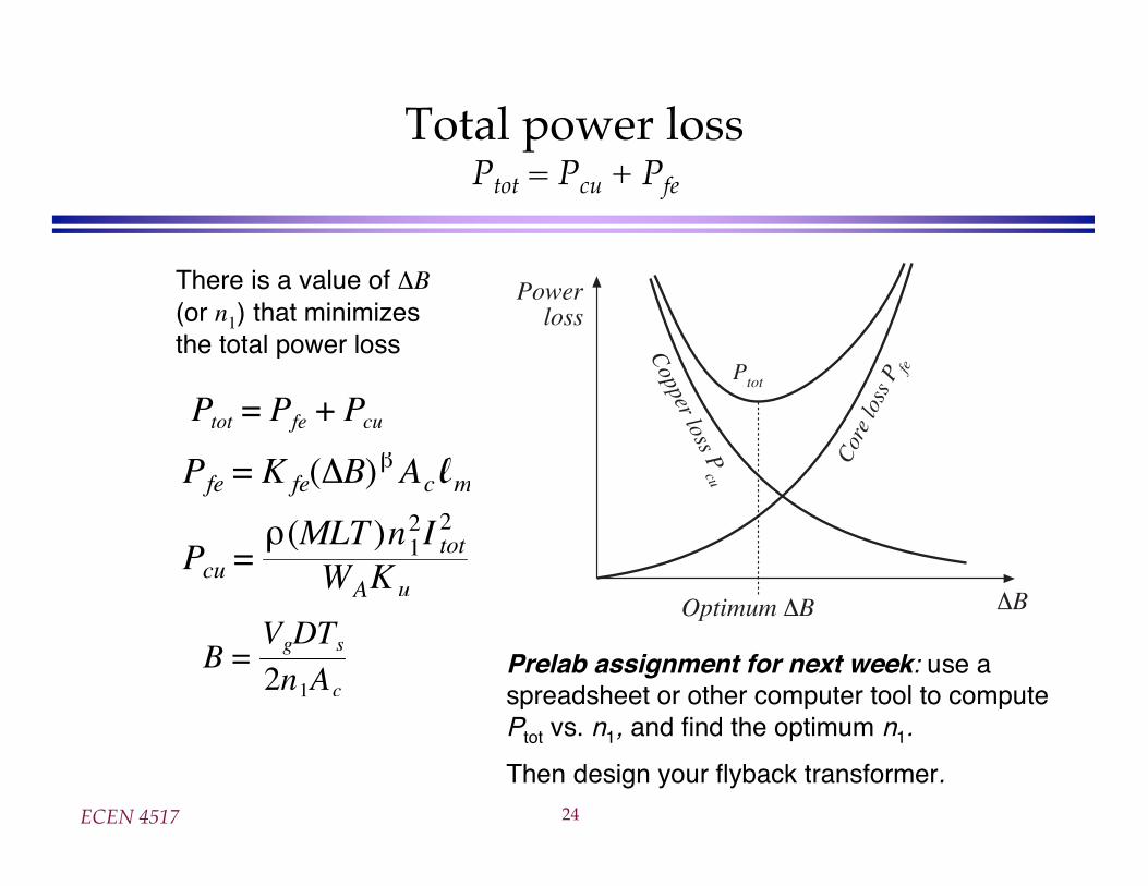
Total power lossPtot = Pcu + Pfe
Ptot = Pfe + Pcu
There is a value of B(or n1) that minimizesthe total power loss
Pfe = K fe(ΔB)β Ac lm
ΔB
Powerloss
Ptot
Copper loss P
cu
Cor
e lo
ss P
fe
Optimum ΔB
Pcu =ρ(MLT )n1
2I tot2
WAK u
�B =VgDTs2n1Ac
Prelab assignment for next week: use aspreadsheet or other computer tool to computePtot vs. n1, and find the optimum n1.
Then design your flyback transformer.
ECEN 4517 25
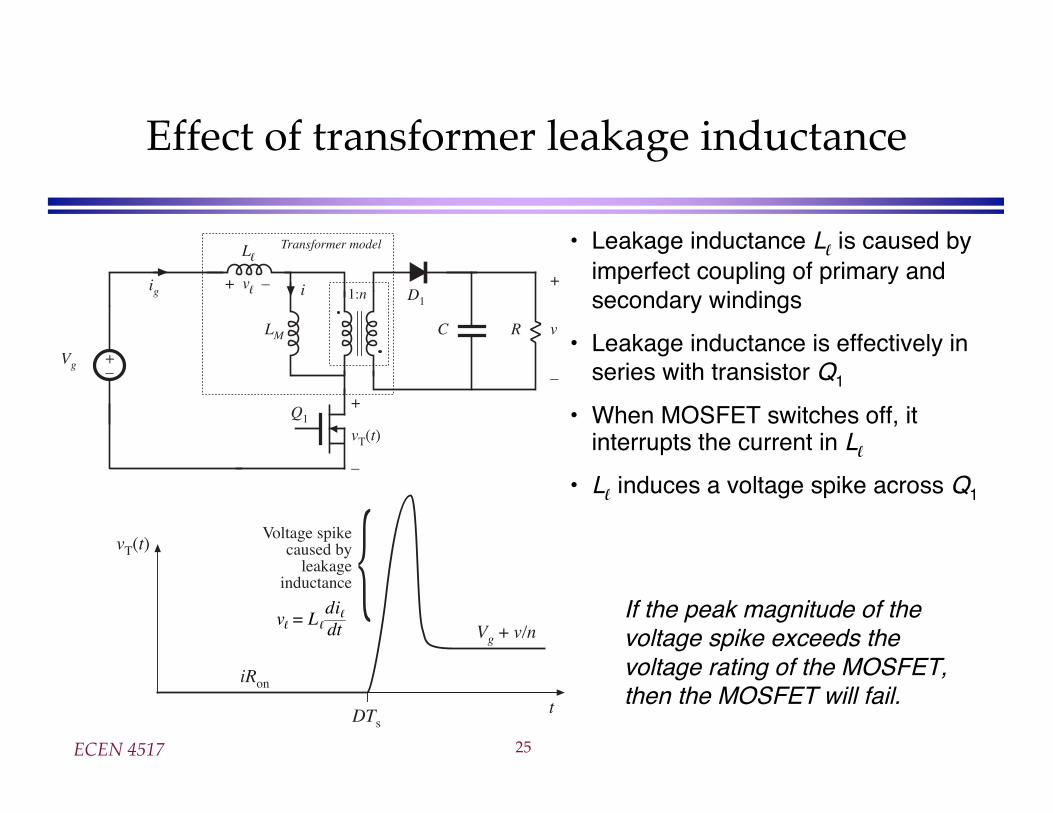
Effect of transformer leakage inductance
+–
LM
+
v
–Vg
Q1
D11:n
C
Transformer model
iig
R
Ll
+ vl –
+
vT(t)
–
• Leakage inductance Ll is caused by
imperfect coupling of primary andsecondary windings
• Leakage inductance is effectively inseries with transistor Q1
• When MOSFET switches off, itinterrupts the current in L
l
• Ll induces a voltage spike across Q1
t
Vg + v/n
vT(t)
iRon
DTs
{Voltage spikecaused by
leakageinductance
vl = L ldildt
If the peak magnitude of thevoltage spike exceeds thevoltage rating of the MOSFET,then the MOSFET will fail.
ECEN 4517 26
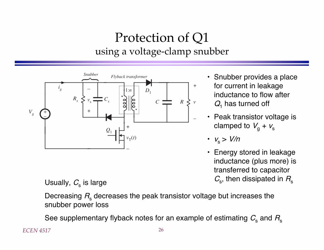
Protection of Q1using a voltage-clamp snubber
+–
+
v
–Vg
Q1
D11:n
C
Flyback transformer
ig
R
+
vT(t)
–
CsRs
–
vs
+
Snubber{ • Snubber provides a placefor current in leakageinductance to flow afterQ1 has turned off
• Peak transistor voltage isclamped to Vg + vs
• vs > V/n
• Energy stored in leakageinductance (plus more) istransferred to capacitorCs, then dissipated in RsUsually, Cs is large
Decreasing Rs decreases the peak transistor voltage but increases thesnubber power loss
See supplementary flyback notes for an example of estimating Cs and Rs
Related Documents