Lecture - 3 PIC18 family architecture and program development

Lecture - 3 PIC18 family architecture and program development.
Dec 24, 2015
Welcome message from author
This document is posted to help you gain knowledge. Please leave a comment to let me know what you think about it! Share it to your friends and learn new things together.
Transcript

Lecture - 3
PIC18 family architecture and program development
Outline
• Overview of the internal PIC architecture.
• The main parts in the PIC microcontroller.
• The register set.
• Assembly language.

Simple microcontroller based system
The PlC microcontroller system normally contains:
• Memory for program and data storage,
• I/O connections to interface with the card reader, LCD display, keyboard, serial interface.
• Timer that can be used as a time-of-day clock and calendar for the system.
• The propose of the system??

Overview of the internal PIC architecture
• The memory in the PlC is divided into two distinct sections: – one for storing the program, and– one for storing data.
• This architecture is called the Harvard architecture.
• The Harvard architecture splits the system memory into two sections to improve system performance.

Harvard vs. von Neumann architecture
• In the traditional von Neumann architecture system, both the data and instructions are fetched through the same bus, which often causes delays because of contentions whenever an instruction manipulates memory data.
• Data and I/O are normally 8 bits in width, whereas instructions are often wider than 8 bits.
• In the Harvard architecture, the data storage and I/O buses are 8 bits wide and the program storage is 16 bits wide.
• This organization allows instructions to be fetched from the program storage in one read cycle or operation to improve efficiency.

Pipelining instructions and executions in the microcontroller
• Because the program memory and data memory are separate, opcode fetches overlap executions.
• This effect is called pipelining.
• During the first instruction cycle clock, instruction 1 is fetched from the memory, then during the second instruction cycle clock, instruction 2 is fetched while instruction 1 executes.
• This overlapping or pipelining allows most instructions to execute in a single clock improving the efficiency of the microcontroller.
•
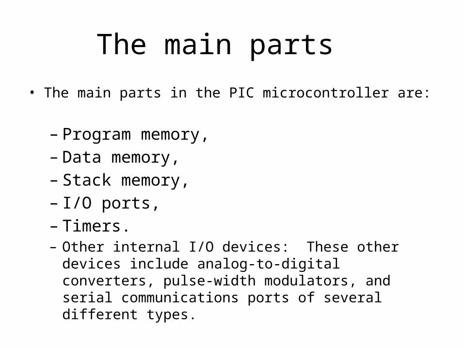
The main parts
• The main parts in the PIC microcontroller are:
– Program memory,– Data memory,– Stack memory,– I/O ports,– Timers.– Other internal I/O devices: These other devices include
analog-to-digital converters, pulse-width modulators, and serial communications ports of several different types.

Program memory (1)• The program memory is 16 bits wide and each location holds most single
word instructions.
• Some instructions require 32 bits of memory or two consecutive memory locations, but most instructions are 16 bits wide.
• The program memory is divided into two parts: – The on-chip program memory.– The external program memory, if needed.
• The amount of on-chip program memory varies between family members from as little as 4K bytes to as much as 128K bytes.
• The on-chip program memory is either flash memory that can be reprogrammed many times in the 18F family or one-time- programmable (OTP) memory in the 18C family.
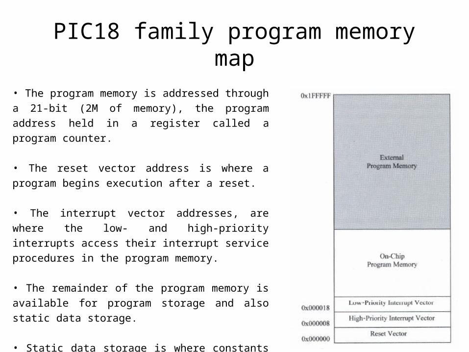
PIC18 family program memory map
• The program memory is addressed through a 21-bit (2M of
memory), the program address held in a register called a
program counter.
• The reset vector address is where a program begins
execution after a reset.
• The interrupt vector addresses, are where the low- and
high-priority interrupts access their interrupt service
procedures in the program memory.
• The remainder of the program memory is available for
program storage and also static data storage.
• Static data storage is where constants and tables of non-
changing data are stored and accessed as data by a program.
Data memory (SRAM)• The data memory is either SRAM or SRAM and EEPROM.
• The data memory provides a place to store transitory data as an application executes and is lost (except for the EEPROM data) when power is removed from the system.
• The data memory SRAM is accessed through a 12-bit address so the largest data memory available is 3968 bytes at address 0x000 through 0xF7F.
• The data memory SRAM also contains addresses that are used to program the special functions of the microcontroller. These special function registers (SFR) are at data memory addresses 0xF80 through 0xFFF or the upper 128 bytes of the data memory space.
• The other data memory locations are called general function registers (GFR) located at addresses 0x000 through 0xF7F. The GFRs are also sometimes called register file locations.

Data memory (EEPROM)
• If a PlC microcontroller contains EEPROM, the EEPROM data
memory is accessed through the special function registers in a
separate address space devoted to the EEPROM.
• The size of the EEPROM is determined by the PlC part number and
ranges from 0 bytes to a maximum of 1024 bytes.
• According to Microchip, a location in the EEPROM can be written
up to one million times.
• The EEPROM locations should only store information that does not
change frequently.
Stack memory
• The stack memory is a small memory of 31 locations, each contains 21-bit.
• The stack memory holds only return addresses from functions.
• The stack is 21 bits wide because it is designed to store program memory addresses.
• 31-deep stack is large enough to function in most applications.
• The only way to use a location on the stack is to call a function.
I/O ports
• The I/O ports are used to interface the microprocessor to the outside world.
• Each I/O port is normally 8 bits in width and can be programmed for inputting or outputting information.
• The number of bits and I/O ports provided varies in different PIC18 family members and is generally determined by the number of pins on the integrated circuit.
• The I/O port programming is accomplished through the special function registers.
Ports directions
• The TRIS register determines the direction (input or output) of each Port pin (TRISA is for Port A, TRISB is for Port B, and so forth).
• When the microcontroller is reset, the TRlS registers are all programmed for input operation, this protects any circuitry attached to the I/O port pin.
• A logic zero in a bit of the TRlS register sets the corresponding Port bit as an output bit, and a logic one in a bit sets the corresponding Port bit as an input bit.
• Once the direction of a port's pins is programmed, the port is accessed by its name, for example, the PORTA register is used to communicate with Port A.

Timers
• Timers are programmable modulus counters which can count events and clock pulses, and perform a variety of services for a program.
• The timers are often programmed to fire (time out) after a certain number of clock pulses have occurred.
• Various PlC family members have between two and five timers.
• Timers are used for a variety of events in a microprocessor, from causing interrupts at a periodic rate for implementing real-time clocks, to measuring unknown frequencies or counting events.
• Timers are also used to generate signals for other devices in a system.

Register set
• The register set controls the microcontroller which contains:
– General purpose registers (GPR).
– Special function registers (SFR).
• The GPR is a set of 8-bit-wide general purpose registers used to store dynamic data.
• All models contains at least GPR locations 0x000 through 0x07F, plus the SFR at 0xF80
through 0xFFF or 256 bytes of SRAM.
• The GPR is accessed through a 12-bit address with the most significant 4 bits containing a
bank location.
• Data memory banks each contain 256 bytes of data memory.
• Data bank 0 contains registers 0x000 through 0x0FF, data bank 1 contains register locations
0x100 through 0x1FF, and so forth.
Access bank
• Access bank: is addressed without using a data bank register, so it is easier to access and more efficient to access in a program.
• These access bank addresses are accessed using a single 8-bit address.
• To access locations in the data RAM outside of the access bank, use a combination of an 8-bit address and the 4-bit bank select register (BSR).
• A bit in an instruction, called the a-bit, selects the access bank (when a = 0) or the bank indicated by the bank select register (when a = 1).
Special Function Registers (SFR)
• The special function registers (SFR) are used to perform a variety of
special tasks in a microcontroller, for example, the bank select
register (BSR).
• SFR can :
– hold a product after a multiplication,
– indicate the status of the outcome of an instruction,
– accumulate results from arithmetic and logic operations, and
– address a location in a program.
• All of the special function registers are located at the top of the data
memory in the access bank. All special function registers have a name
and an address, where either can be used for accessing them.

Accumulator (WREG)
• The accumulator or, as it is often called, the working register (W register or
WREG) is an 8-bit register that is accessed by many instructions.
• This register is most likely called an accumulator because it is where results
accumulate for many instructions.
• Most CPUs contain an accumulator as the main working register. In the PIC18
family, the working register (WREG) is located in the SFR area at address 0xFE8.
• Although this register is assigned an address, many instructions access it without
using its address by its name or implicitly as part of an instruction.
• This implicit form of addressing is why WREG is called the working register or
accumulator.
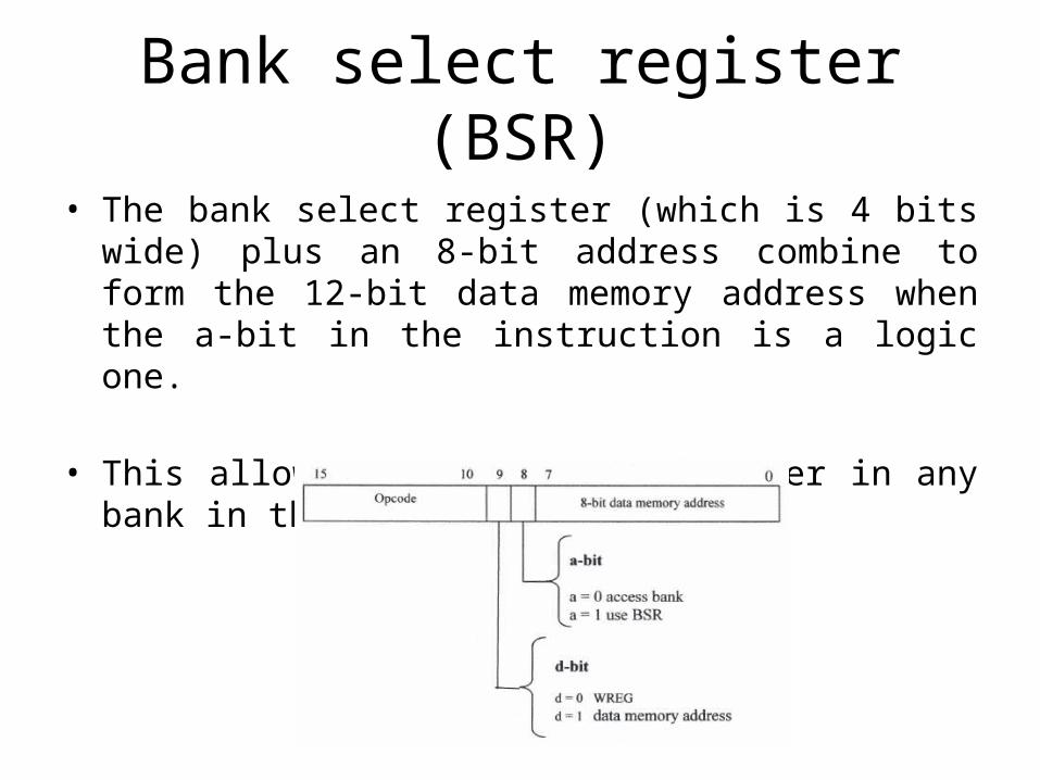
Bank select register (BSR)
• The bank select register (which is 4 bits wide) plus an 8-bit address combine to form the 12-bit data memory address when the a-bit in the instruction is a logic one.
• This allows access to any register in any bank in the data memory.
Product registers
• The product registers hold the result or product after the multiply instruction executes.
• A special register is needed for multiplication because a product is always twice the width of the multiplier.
• The MULLW instruction multiplies the W register by the literal value.
• Because this is an 8-bit microcontroller and the multiplication is 8 bits, the product is 16 bits in width and stored in the PRODL and PRODH registers.
Status registers (SR)
• The status register (SR) indicates the outcome of an operation.
• Only five of the eights bits indicate status and are labeled N (negative),
OV (overflow), Z (zero), DC (digit carry), and C (carry).
• The status bits are tested by the conditional branch instructions that are
most often used to form the if-then-else construct in programming as
well as other programming constructs.
• The status register bits will normally change only for an arithmetic or
logic operation in the PlC.
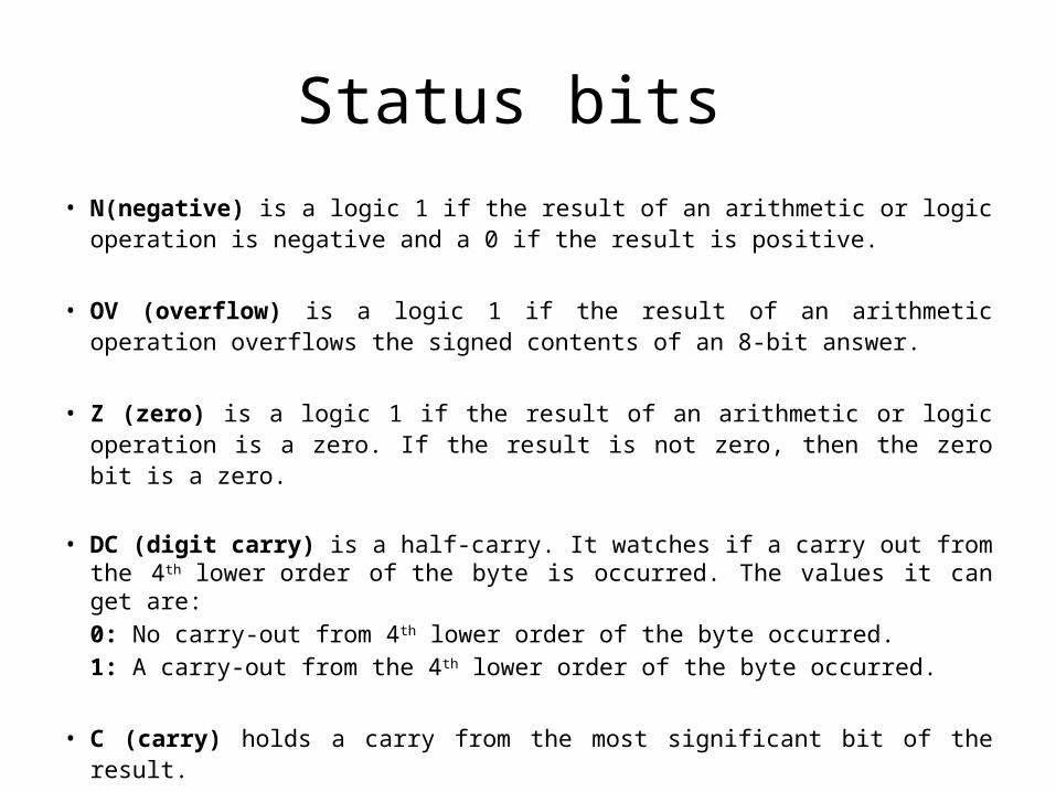
Status bits
• N(negative) is a logic 1 if the result of an arithmetic or logic operation is negative and a 0 if the result is positive.
• OV (overflow) is a logic 1 if the result of an arithmetic operation overflows the signed contents of an 8-bit answer.
• Z (zero) is a logic 1 if the result of an arithmetic or logic operation is a zero. If the result is not zero, then the zero bit is a zero.
• DC (digit carry) is a half-carry. It watches if a carry out from the 4th lower order of the byte is occurred. The values it can get are:
0: No carry-out from 4th lower order of the byte occurred.
1: A carry-out from the 4th lower order of the byte occurred.
• C (carry) holds a carry from the most significant bit of the result.

Program counter (PC)
• The program counter, a 2l-bit register in the PlC 18 family, addresses the next location in the program memory and allows instructions to be accessed sequentially from the program memory.
• The program counter is a counter, but does not count programs. It counts up through the memory to access the next instruction in a program, which is probably why it is named the program counter.
• In some machines, this register is more appropriately called the instruction address register (IAR).
• The flow of a program is modified if the contents of the program counter are changed.

The integrated development environment (IDE)
• The software development system used to generate programs for the PlC microcontroIIer is called the integrated development environment or IDE.
• The IDE provides an editor to: – enter program code, – access to the programmer to program the code onto the PlC
microcontroller, – and access to a simulator to allow a program to be
emulated in the personal computer before it is programmed.

Assembly language
• The assembler is a program that converts assembly language (symbolic machine code) from a source file into numeric machine code stored in an object file.
• The source file for the assembler is usually a file that uses the file extension of .asm, and the object file generated by the assembler usually has the extension of .O.
• The executable program file is a file for flashing the microcontroller, usually in the Intel hex format, which is generated by another program called a linker.
• The linker program combines multiple object files from the assembler and C language into a single executable file.
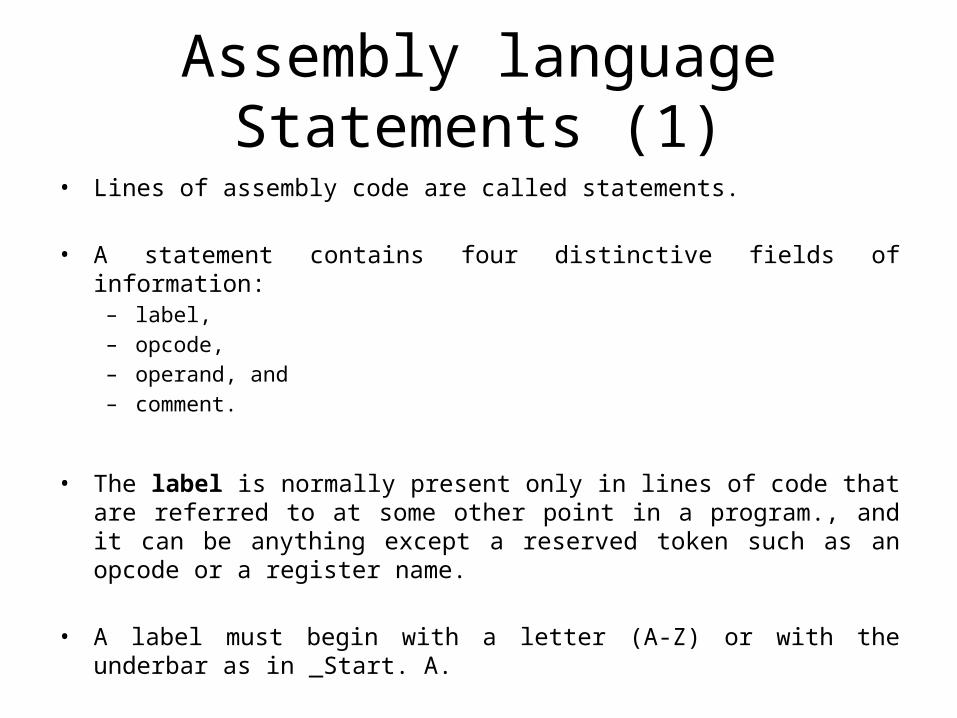
Assembly language Statements (1)
• Lines of assembly code are called statements.
• A statement contains four distinctive fields of information:– label, – opcode, – operand, and – comment.
• The label is normally present only in lines of code that are referred to at some other point in a program., and it can be anything except a reserved token such as an opcode or a register name.
• A label must begin with a letter (A-Z) or with the underbar as in _Start. A.
• label can contain any letter, a number, an underbar, or a question mark. Labels usually end with a colon, but this is optional.
Assembly language Statements (2)
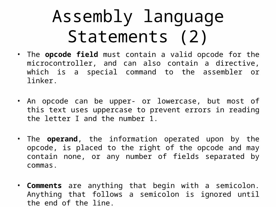
• The opcode field must contain a valid opcode for the microcontroller, and can also contain a directive, which is a special command to the assembler or linker.
• An opcode can be upper- or lowercase, but most of this text uses uppercase to prevent errors in reading the letter I and the number 1.
• The operand, the information operated upon by the opcode, is placed to the right of the opcode and may contain none, or any number of fields separated by commas.
• Comments are anything that begin with a semicolon. Anything that follows a semicolon is ignored until the end of the line.
• Directives are special commands to the assembler that may or may not generate machine code.
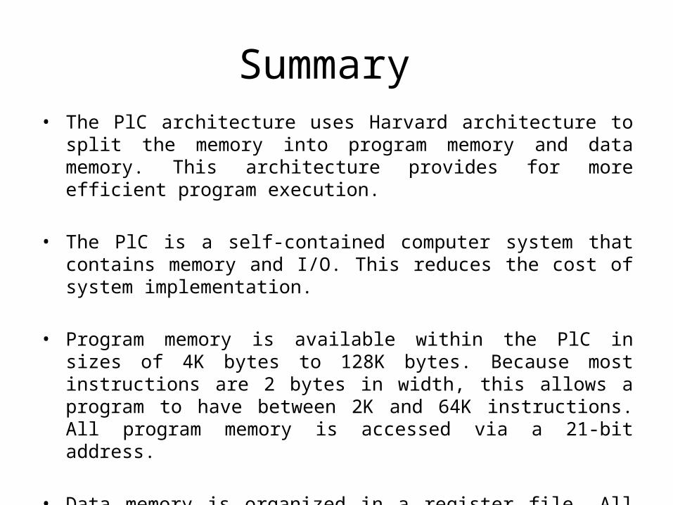
Summary • The PlC architecture uses Harvard architecture to split the memory into
program memory and data memory. This architecture provides for more efficient program execution.
• The PlC is a self-contained computer system that contains memory and I/O. This reduces the cost of system implementation.
• Program memory is available within the PlC in sizes of 4K bytes to 128K bytes. Because most instructions are 2 bytes in width, this allows a program to have between 2K and 64K instructions. All program memory is accessed via a 21-bit address.
• Data memory is organized in a register file. All data memory is 8 bits in width and varies in size from 256 bytes to 3840 bytes plus an additional 128 bytes for the special function registers. All data memory is accessed via a 12-bit address.
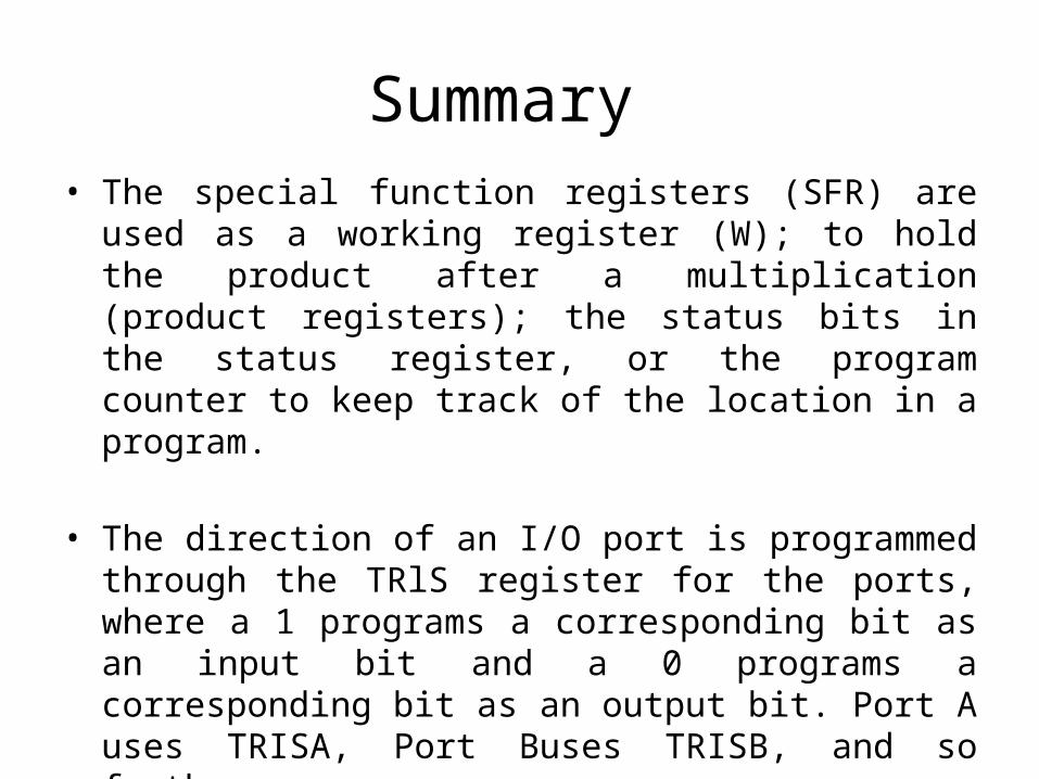
Summary • The special function registers (SFR) are used as a working
register (W); to hold the product after a multiplication (product registers); the status bits in the status register, or the program counter to keep track of the location in a program.
• The direction of an I/O port is programmed through the TRlS register for the ports, where a 1 programs a corresponding bit as an input bit and a 0 programs a corresponding bit as an output bit. Port A uses TRISA, Port Buses TRISB, and so forth.
• Data are read or written to I/O port pins by using the PORTA register for Port A or the PORTB register for Port B.
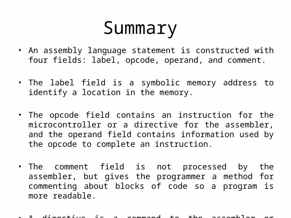
Summary • An assembly language statement is constructed with four fields: label,
opcode, operand, and comment.
• The label field is a symbolic memory address to identify a location in the memory.
• The opcode field contains an instruction for the microcontroller or a directive for the assembler, and the operand field contains information used by the opcode to complete an instruction.
• The comment field is not processed by the assembler, but gives the programmer a method for commenting about blocks of code so a program is more readable.
• A directive is a command to the assembler or linker that often generates no code for the program or data memory.

Questions
1. Select an option that makes the statement TRUE:
- Pipelining:
a. Do not allow most instructions to be executed in a single clock.
b. Improve the efficiency of the microcontroller.
c. Increase the instructions execution time.
d. None of the above.
.
2. Select an option that makes the statement NOT TRUE:
- This is a field in the assembly language statements:
a. label.
b. opcode.
c. comment.
d. PIC part number.
Questions
1. Which of the following labels are valid?
a. 2FAR
b. FAR A WAY
c. FAR_A_WAY
d. FarAWay
2. Given the following assembly language statements, identify the field of each section of the statement:
a. Start: GOTO Heaven
b. ADDLW Ox29 ;add a Ox29
c. Loopyl: MOVFF WREG,0x145 ;a move in action
Questions
3. How is the TRISB register programmed to select the output operation for Port B bits 0 through 2 and input operation for Port B pins 3 through 7?
Related Documents


