Lecture 3 Capacitance Calculation

Lecture 3 Capacitance Calculation. References Detailed Load Capacitance Calculation (Hodges,Section 6.3) Detailed MOS Capacitance Model (West, Section.
Dec 22, 2015
Welcome message from author
This document is posted to help you gain knowledge. Please leave a comment to let me know what you think about it! Share it to your friends and learn new things together.
Transcript

Lecture 3
Capacitance Calculation
References
• Detailed Load Capacitance Calculation (Hodges,Section 6.3)
• Detailed MOS Capacitance Model (West, Section 2.3.2)

Identification of Various Capacitances

Data-Dependent Gate Capacitance
• Effective Gate Capacitance (i.e. capacitance into the gate) in a 0.35 um process

General Capacitance Model
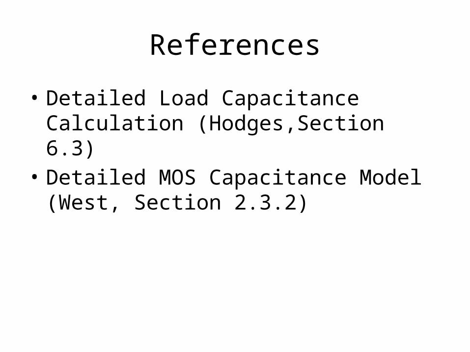
Typo: 2/3
General Capacitance Model:1. Thin-Oxide Capacitance
a. Voltage dependent (Cgs, Cgd, Cgb)b. Voltage independent: Col
2. Junction Capacitance (Cjsb, Cjdb)
Cgs,Cgd and Cgb
Channel extends fromsource to drain
Channel almostfrom source to drain
Cg in series with Cj
C(0V)=0.5Cg
Gate:-QUnder SiO2:Q
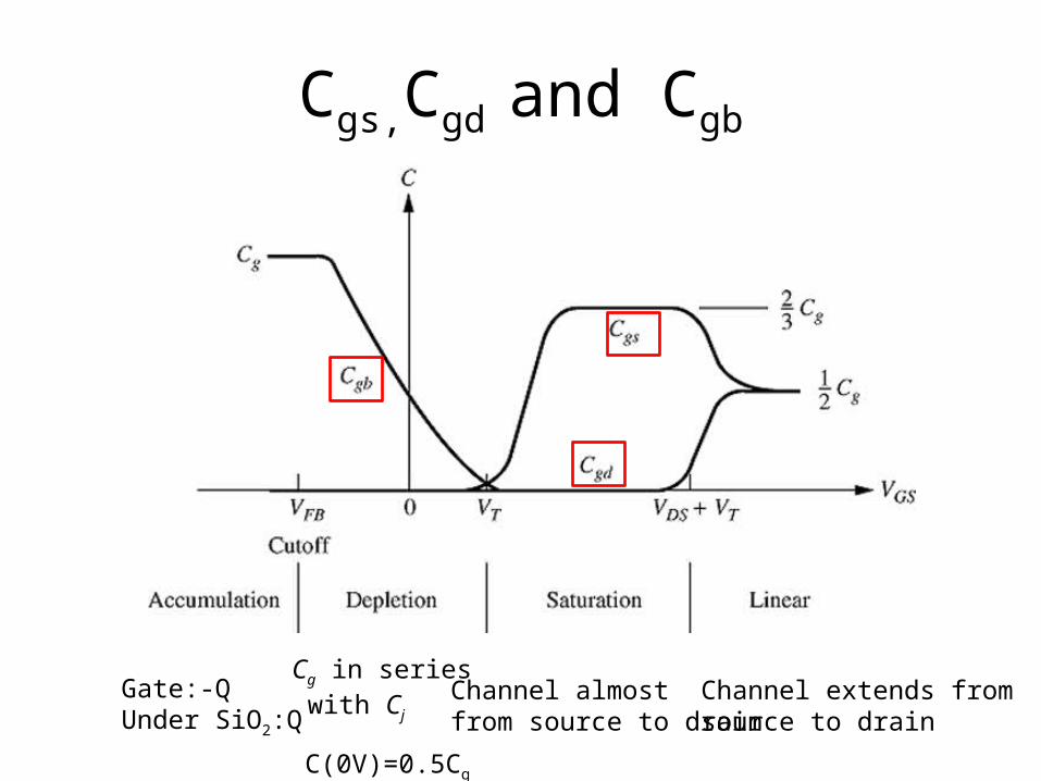
Intuition about Junction Capacitance
• The depletion region is narrower when the diode is forward biased, therefore the junction diode capacitance is higher.
• The depletion region is wider when the diode is reverse biased, therefore the junction diode capacitance is smaller.

Junction capacitance versus applied voltage
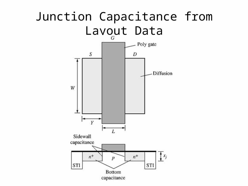
Junction Capacitance from Layout Data
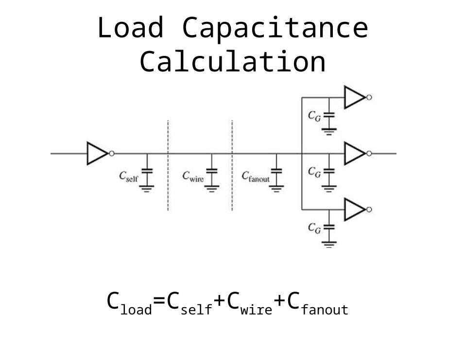
Load Capacitance Calculation
Cload=Cself+Cwire+Cfanout

Fanout Capacitance
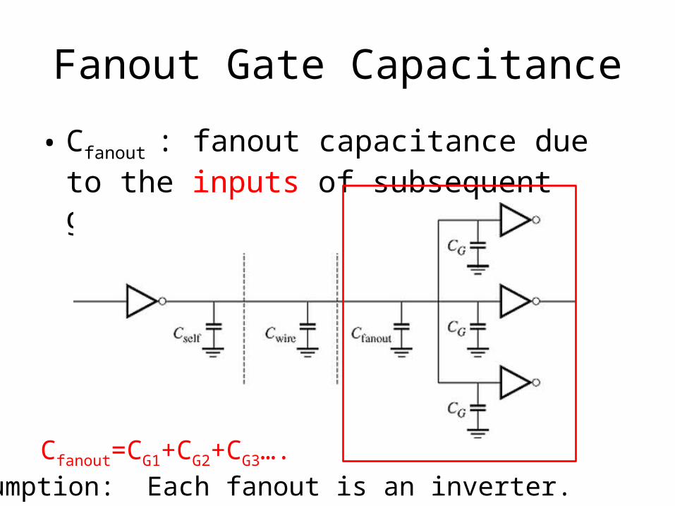
Fanout Gate Capacitance
• Cfanout : fanout capacitance due to the inputs of subsequent gates, CG.
Cfanout=CG1+CG2+CG3….Assumption: Each fanout is an inverter.
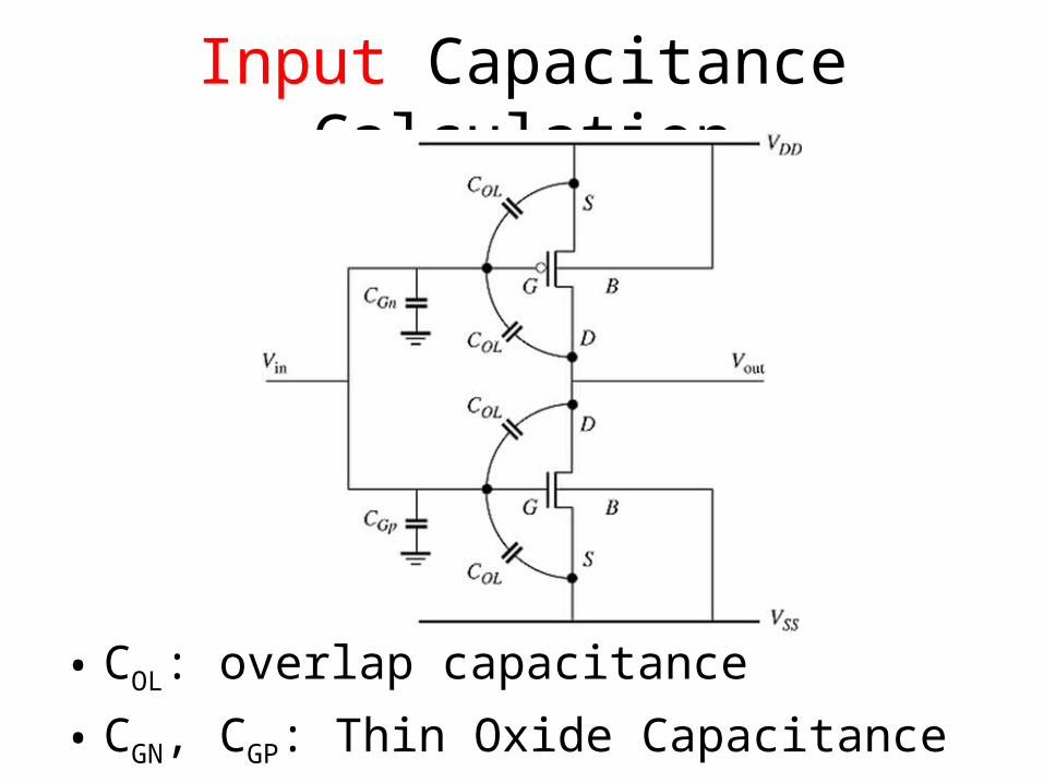
Input Capacitance Calculation
• COL: overlap capacitance
• CGN, CGP: Thin Oxide Capacitance

Worst Case Analysis Assumption
• The thin-oxide capacitance is voltage dependent.
• The worst case analysis uses CoxWL to compute its worst case value.
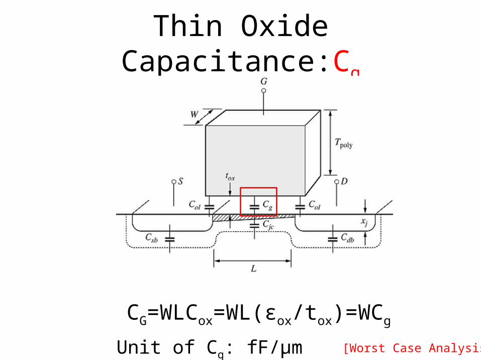
Thin Oxide Capacitance:Cg
CG=WLCox=WL(εox/tox)=WCg
Unit of Cg: fF/μm [Worst Case Analysis]

Cg
tox L Cg
110 nm 5 1.61 fF/μm
7.5 nm 0.35 μm 1.65 fF/μm
2.2 nm 0.1 μm 1.61 fF/μm
Cg is approximately 1.61 fF/μm for the last 25 years.Exception: the 0.18 μm process, which has a Cg of 1.0 fF/ μm.
[Worst Case Analysis]

Thin Oxide Capacitance:Col
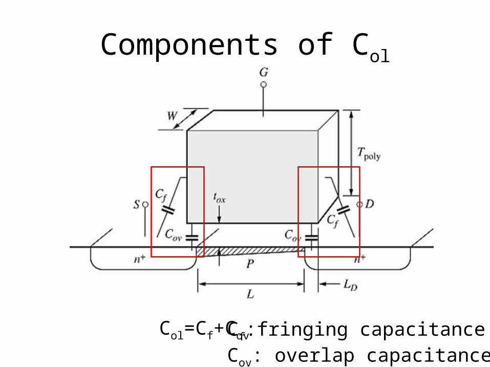
Components of Col
Col=Cf+Cov Cf:fringing capacitanceCov: overlap capacitance

Redefine Cg
• For 0.13 μm,– Cg (due to tox alone): 1.6 fF/μm [Hodges, p.72]
– Col(due to Cov and Cf): 0.25 fF/ μm [Hodges, p.80]– Redefine Cg [Hodges, p.259] as• Cg=CoxL+2Col
• Cg =1.6 fF/μm+ 2 0.25 fF/μm=2 fF/μm
• Cg has been constant for over 20 years
– Multipy Cg by W to obtain the total capacitance due to tox, Cov and Cf
[Worst Case Analysis]
[Worst Case Analysis]

Gate Capacitance of an Inverter
• CG=Cg(Wn+Wp)
• CG=2fF/μm(Wn+Wp)
[Worst Case Analysis]

Fanout Gate capacitance of n Inverters
• Cfanout=2fF/μm[(Wn+Wp)1+(Wn+Wp)2…(Wn+Wp)n]
[Worst Case Analysis]
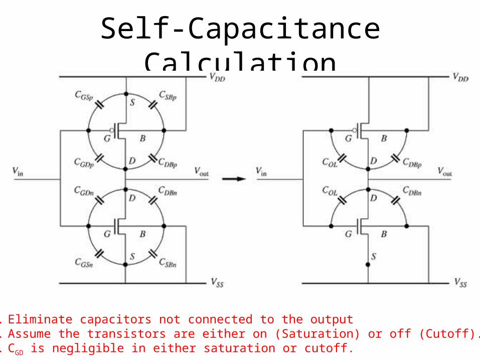
Self-Capacitance Calculation
1. Eliminate capacitors not connected to the output2. Assume the transistors are either on (Saturation) or off (Cutoff). 3. CGD is negligible in either saturation or cutoff.

Miller Capacitance

Derivation of Miller Capacitance
Z1=/Z(1-Vy/Vx)
Z2=/Z(1-Vx/Vy)
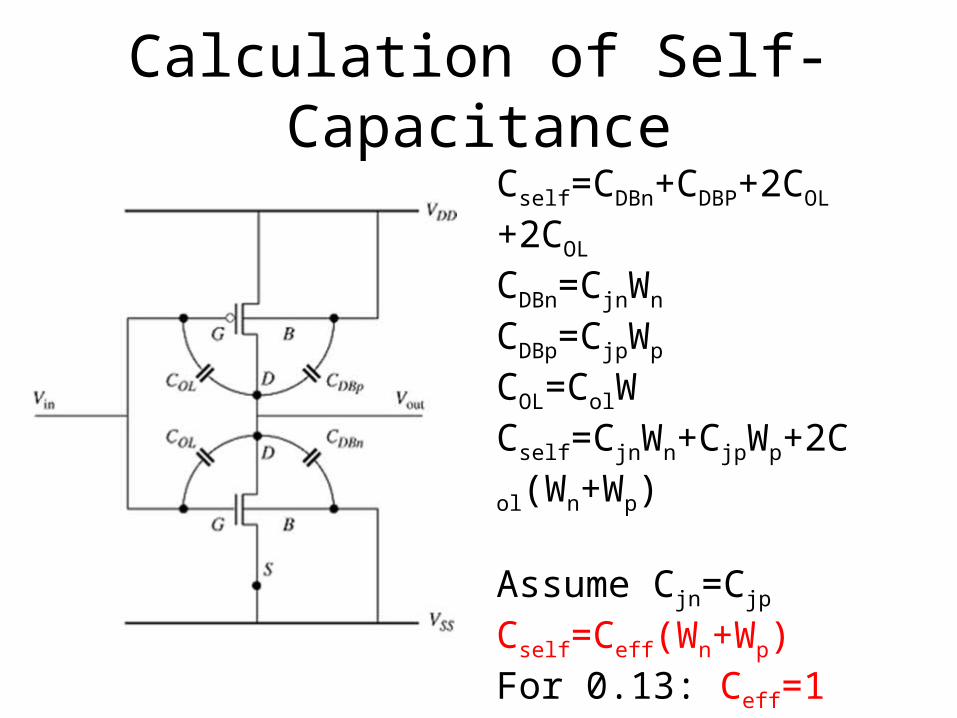
Calculation of Self-CapacitanceCself=CDBn+CDBP+2COL+2CO
L
CDBn=CjnWn
CDBp=CjpWp
COL=ColWCself=CjnWn+CjpWp+2Col(Wn+Wp)
Assume Cjn=Cjp
Cself=Ceff(Wn+Wp)For 0.13: Ceff=1 fF/μm [Hodges, p. 261]

Wire Capacitance
• Ignore wire capacitance if the length of a wire is less than a few microns.
• Include wires longer than a few microns– Cwire=CintLwire
– Cint=0.2 fF/um
• For very long wires use distributed model
Related Documents