1 Electronics II (ELE 343 – Lecture 2)

Welcome message from author
This document is posted to help you gain knowledge. Please leave a comment to let me know what you think about it! Share it to your friends and learn new things together.
Transcript

1
Electronics II
(ELE 343 – Lecture 2)

2
Amplifier Example I
➢ The keys in solving this problem are recognizing the AC
ground between R1 and R2, and Thevenin transformation of
the input network.

3
Current Sources
▪ Ideal Current Sources
II V
V
I
[I-V curve]
(Definition)
A current source is an electronic circuit that delivers or absorbs an electric current
which is independent of the voltage across it.
What is the output impedance for the current source?
➔ Ideally, it’s infinite.
What happens if the output impedance is not infinite?

4
Current Sources
▪Why do we need a Current Source?

5
Current Sources
▪Current source by using BJTs
➢ Ideally, IC does not depend on the collector to emitter voltage.
➢ This property allows the transistor to behave as a constant current source when its base-emitter voltage is fixed.
6
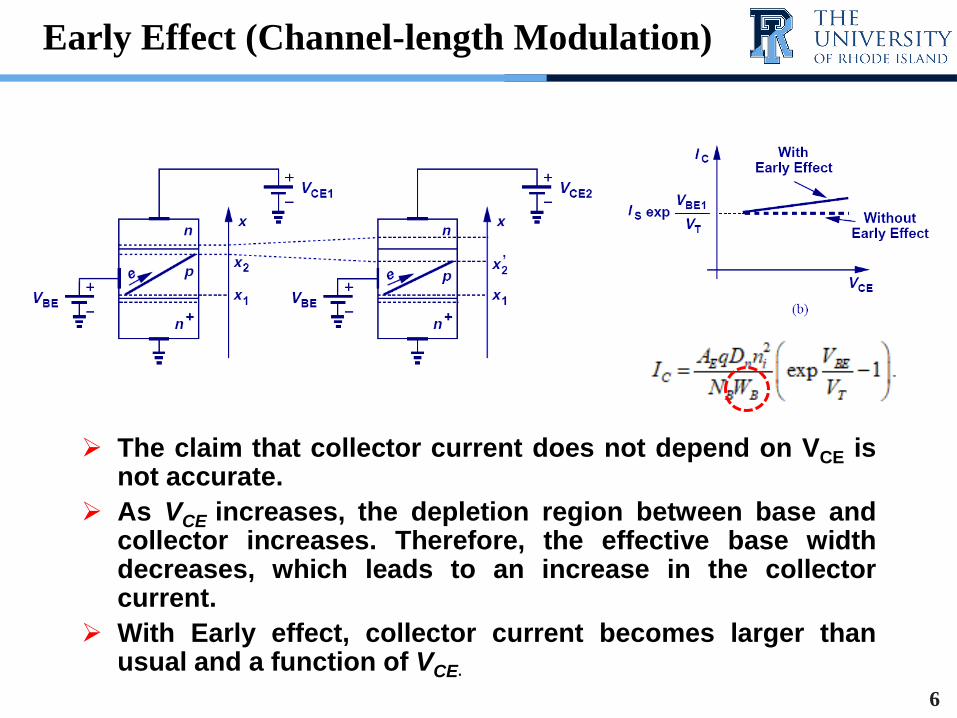
➢ The claim that collector current does not depend on VCE isnot accurate.
➢ As VCE increases, the depletion region between base andcollector increases. Therefore, the effective base widthdecreases, which leads to an increase in the collectorcurrent.
➢ With Early effect, collector current becomes larger thanusual and a function of VCE.
Early Effect (Channel-length Modulation)
7
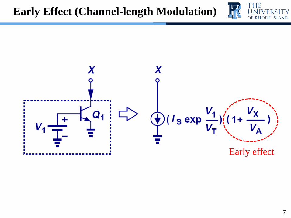
Early Effect (Channel-length Modulation)
Early effect
9
Early Effect (Channel-length Modulation)
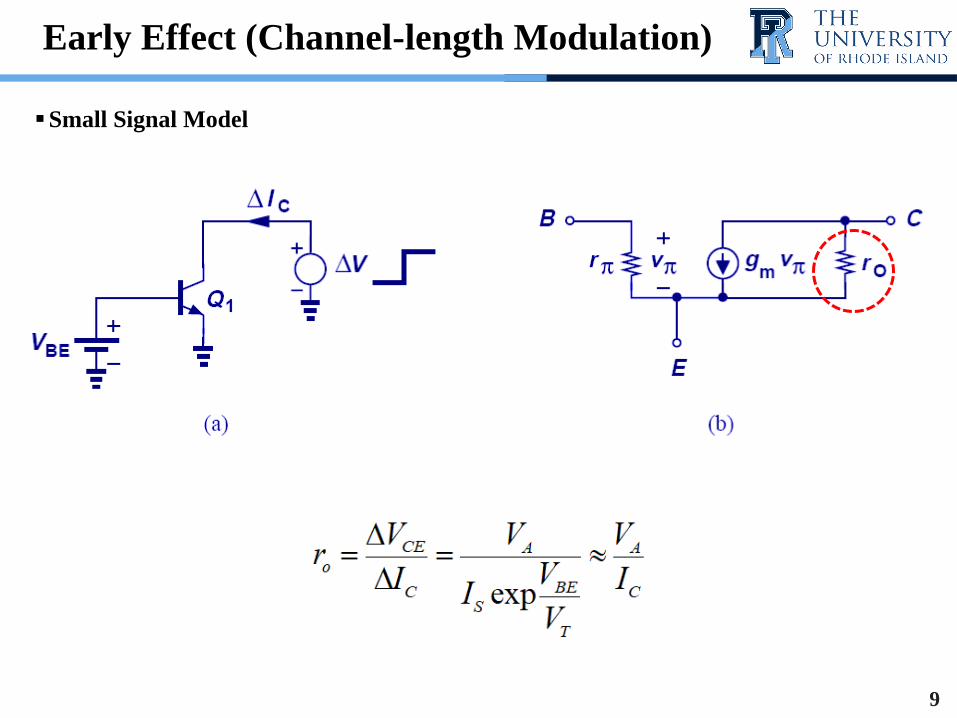
▪Small Signal Model

10
➢ With Early effect, collector current becomes larger than
usual and a function of VCE.
Early Effect (Channel-length Modulation)

11
Output Impedance of Degenerated Stage
➢ Emitter degeneration boosts the output impedance by afactor of 1+gm(RE||r).
➢ This improves the gain of the amplifier and makes thecircuit a better current source.
➢ Rout?

12
Boosted Output Impedances
➢ Pros & Cons of RE / RS
Pros
Large output impedance
➔ Being close to ideal CS
Cons
Narrow operating range

14
Bipolar Cascode Stage
➢ Rout?
Degeneration Tr
Cascode Tr

15
Example 9.1
➢ If Q1 and Q2 are biased at a collector current of 1 mA, determine the
output resistance.
Assume β = 100 and VA = 5 V for both transistors.

16
Max. Bipolar Cascode Output Impedance
➢ The maximum output impedance of a bipolar cascode is
bounded by the ever-present r between emitter and ground
of Q1.
➢ Rout,max?
17
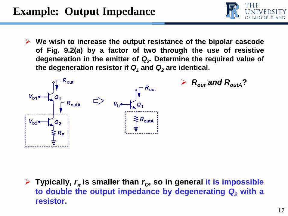
Example: Output Impedance
➢ Typically, r is smaller than rO, so in general it is impossible
to double the output impedance by degenerating Q2 with a
resistor.
➢ We wish to increase the output resistance of the bipolar cascode
of Fig. 9.2(a) by a factor of two through the use of resistive
degeneration in the emitter of Q2. Determine the required value of
the degeneration resistor if Q1 and Q2 are identical.
➢ Rout and RoutA?

18
Example: Mixed BJT/MOS Cascode
2
1
➢ RoutA? ➢ RoutB?

19
PNP Cascode Stage
Degeneration Tr
Cascode Tr
➢ Rout?

20
Another Interpretation of Bipolar Cascode
➢ Instead of treating cascode as Q2 degenerating Q1, we can
also think of it as Q1 stacking on top of Q2 (current source)
to boost Q2’s output impedance.

21
False Cascodes
➢ When the emitter of Q1 is connected to the emitter of Q2, it’s
no longer a cascode since Q2 becomes a diode-connected
device instead of a current source.
➢ Rout?
22
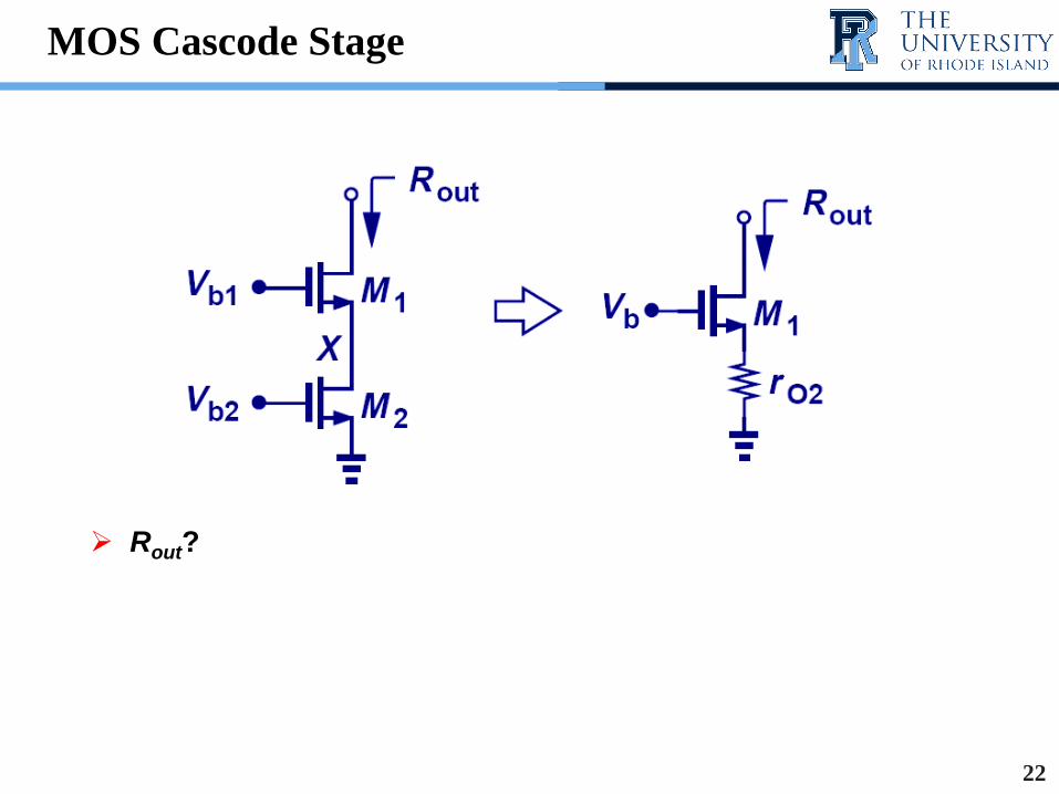
MOS Cascode Stage
➢ Rout?

23
Example: MOS Cascades
➢ Design an NMOS cascode for an output impedance of 500
kΩ and a current of 0.5 mA. For simplicity, assume M1 and
M2 are identical (they need not be).
Assume μnCox = 100 μA/V2 and λ = 0.1V−1.

24
Another Interpretation of MOS Cascode
➢ Similar to its bipolar counterpart, MOS cascode can be thought ofas stacking a transistor on top of a current source.
➢ Unlike bipolar cascode, the output impedance is not limited by .
25
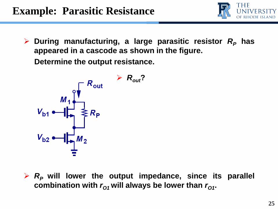
Example: Parasitic Resistance
➢ RP will lower the output impedance, since its parallel
combination with rO1 will always be lower than rO1.
➢ During manufacturing, a large parasitic resistor RP has
appeared in a cascode as shown in the figure.
Determine the output resistance.
➢ Rout?
Related Documents