Lecture 16: Circuit Pitfalls

Welcome message from author
This document is posted to help you gain knowledge. Please leave a comment to let me know what you think about it! Share it to your friends and learn new things together.
Transcript
Lecture 16: Circuit Pitfalls
16: Circuit Pitfalls 2CMOS VLSI DesignCMOS VLSI Design 4th Ed.
OutlineVariationNoise BudgetsReliabilityCircuit Pitfalls
16: Circuit Pitfalls 3CMOS VLSI DesignCMOS VLSI Design 4th Ed.
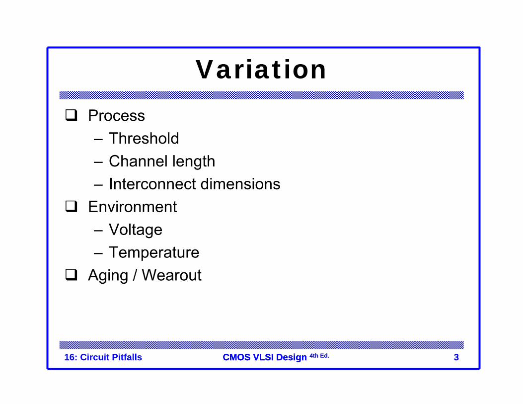
VariationProcess– Threshold– Channel length– Interconnect dimensions
Environment– Voltage– Temperature
Aging / Wearout
16: Circuit Pitfalls 4CMOS VLSI DesignCMOS VLSI Design 4th Ed.
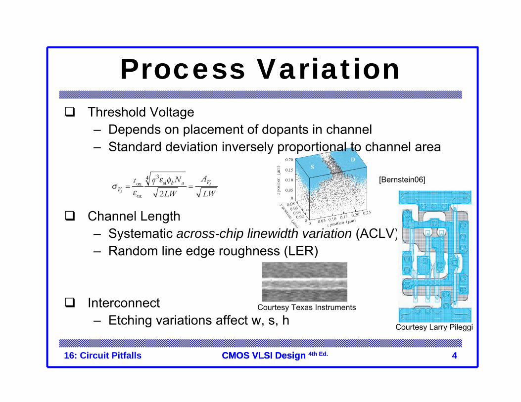
Process VariationThreshold Voltage– Depends on placement of dopants in channel– Standard deviation inversely proportional to channel area
Channel Length– Systematic across-chip linewidth variation (ACLV)– Random line edge roughness (LER)
Interconnect– Etching variations affect w, s, h
[Bernstein06]
Courtesy Texas Instruments
Courtesy Larry Pileggi

16: Circuit Pitfalls 5CMOS VLSI DesignCMOS VLSI Design 4th Ed.
Spatial DistributionVariations show spatial correlation– Lot-to-lot (L2L)– Wafer-to-wafer (W2W)– Die-to-die (D2D) / inter-die– Within-die (WID) / intradie
Closer transistors match better
Courtesy M. Pelgrom

16: Circuit Pitfalls 6CMOS VLSI DesignCMOS VLSI Design 4th Ed.
Environmental VariationVoltage– VDD is usually designed +/- 10%– Regulator error– On-chip droop from
switching activityTemperature– Ambient temperature ranges– On-die temperature elevated
by chip power consumption
Courtesy IBM
[Harris01b]
16: Circuit Pitfalls 7CMOS VLSI DesignCMOS VLSI Design 4th Ed.
AgingTransistors change over time as they wear out– Hot carriers– Negative bias temperature instability– Time-dependent dielectric breakdown
Causes threshold voltage changesMore on this later…
16: Circuit Pitfalls 8CMOS VLSI DesignCMOS VLSI Design 4th Ed.
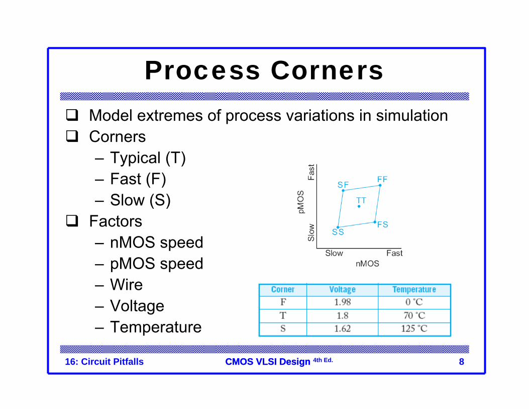
Process CornersModel extremes of process variations in simulationCorners– Typical (T)– Fast (F)– Slow (S)
Factors– nMOS speed– pMOS speed– Wire– Voltage– Temperature
16: Circuit Pitfalls 9CMOS VLSI DesignCMOS VLSI Design 4th Ed.
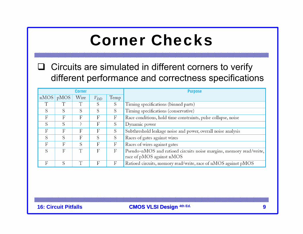
Corner ChecksCircuits are simulated in different corners to verify different performance and correctness specifications
16: Circuit Pitfalls 10CMOS VLSI DesignCMOS VLSI Design 4th Ed.
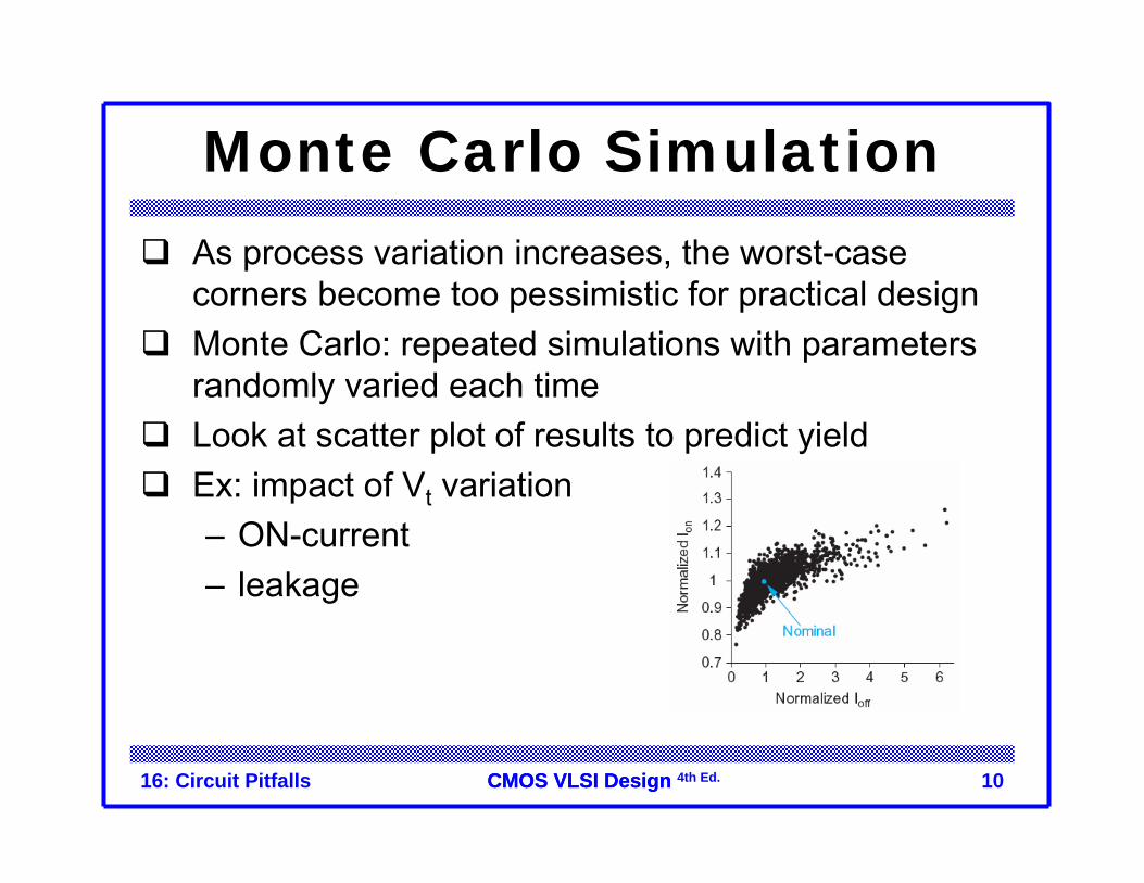
Monte Carlo SimulationAs process variation increases, the worst-case corners become too pessimistic for practical designMonte Carlo: repeated simulations with parameters randomly varied each timeLook at scatter plot of results to predict yieldEx: impact of Vt variation– ON-current– leakage
16: Circuit Pitfalls 11CMOS VLSI DesignCMOS VLSI Design 4th Ed.
NoiseSources– Power supply noise / ground bounce– Capacitive coupling– Charge sharing– Leakage– Noise feedthrough
Consequences– Increased delay (for noise to settle out)– Or incorrect computations
16: Circuit Pitfalls 12CMOS VLSI DesignCMOS VLSI Design 4th Ed.
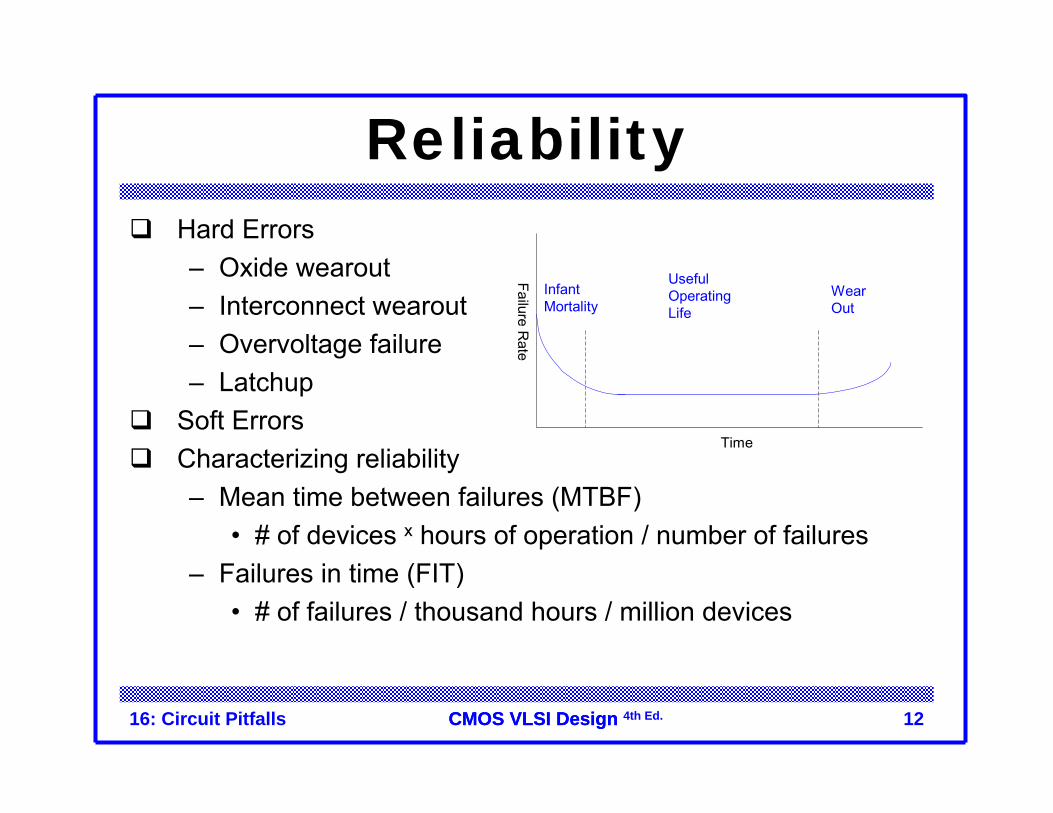
ReliabilityHard Errors– Oxide wearout– Interconnect wearout– Overvoltage failure– Latchup
Soft ErrorsCharacterizing reliability– Mean time between failures (MTBF)
• # of devices x hours of operation / number of failures– Failures in time (FIT)
• # of failures / thousand hours / million devices
Time
Failure Rate
InfantMortality
UsefulOperatingLife
WearOut
16: Circuit Pitfalls 13CMOS VLSI DesignCMOS VLSI Design 4th Ed.
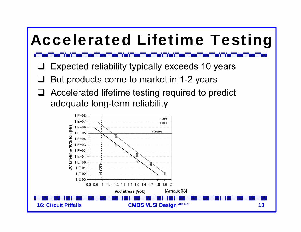
Accelerated Lifetime TestingExpected reliability typically exceeds 10 yearsBut products come to market in 1-2 yearsAccelerated lifetime testing required to predict adequate long-term reliability
[Arnaud08]
16: Circuit Pitfalls 14CMOS VLSI DesignCMOS VLSI Design 4th Ed.
Hot CarriersElectric fields across channel impart high energies to some carriers– These “hot” carriers may be blasted into the gate
oxide where they become trapped– Accumulation of charge in oxide causes shift in Vt
over time– Eventually Vt shifts too far for devices to operate
correctlyChoose VDD to achieve reasonable product lifetime– Worst problems for inverters and NORs with slow
input risetime and long propagation delays

16: Circuit Pitfalls 15CMOS VLSI DesignCMOS VLSI Design 4th Ed.
NBTINegative bias temperature instabilityElectric field applied across oxide forms dangling bonds called traps at Si-SiO2 interfaceAccumulation of traps causes Vt shiftMost pronounced for pMOS transistors with strong negative bias (Vg = 0, Vs = VDD) at high temperature
16: Circuit Pitfalls 16CMOS VLSI DesignCMOS VLSI Design 4th Ed.
TDDBTime-dependent dielectric breakdown– Gradual increase in gate leakage when an
electric field is applied across an oxide– a.k.a stress-induced leakage current
For 10-year life at 125 C, keep Eox below ~0.7 V/nm

16: Circuit Pitfalls 17CMOS VLSI DesignCMOS VLSI Design 4th Ed.
Electromigration“Electron wind” causes movement of metal atoms along wiresExcessive electromigration leads to open circuitsMost significant for unidirectional (DC) current– Depends on current density Jdc (current / area)– Exponential dependence on temperature
– Black’s Equation:
– Typical limits: Jdc < 1 – 2 mA / μm2
aEkT
ndc
eMTTFJ
∝
[Christiansen06]
16: Circuit Pitfalls 18CMOS VLSI DesignCMOS VLSI Design 4th Ed.
Electromigration Video
16: Circuit Pitfalls 19CMOS VLSI DesignCMOS VLSI Design 4th Ed.
Electromigration Video 2

16: Circuit Pitfalls 20CMOS VLSI DesignCMOS VLSI Design 4th Ed.
Self-HeatingCurrent through wire resistance generates heat– Oxide surrounding wires is a thermal insulator– Heat tends to build up in wires– Hotter wires are more resistive, slower
Self-heating limits AC current densities for reliability
– Typical limits: Jrms < 15 mA / μm2
2
0
( )T
rms
I t dtI
T=∫
16: Circuit Pitfalls 21CMOS VLSI DesignCMOS VLSI Design 4th Ed.
Overvoltage FailureHigh voltages can blow out tiny transistorsElectrostatic discharge (ESD)– kilovolts from static electricity when the package
pins are handledOxide breakdown– In a 65 nm process, Vg ≈ 3 V causes arcing
through thin gate oxidesPunchthrough– High Vds causes depletion region between source
and drain to touch, leading to high current flow and destructive overheating
16: Circuit Pitfalls 22CMOS VLSI DesignCMOS VLSI Design 4th Ed.
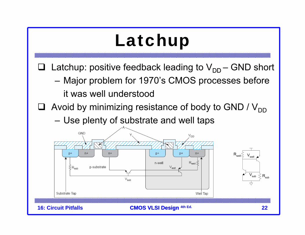
Latchup
Rsub
Rwell
Vsub
Vwell
Latchup: positive feedback leading to VDD DD – GND short– Major problem for 1970’s CMOS processes before
it was well understoodAvoid by minimizing resistance of body to GND / VDD
– Use plenty of substrate and well taps
16: Circuit Pitfalls 23CMOS VLSI DesignCMOS VLSI Design 4th Ed.
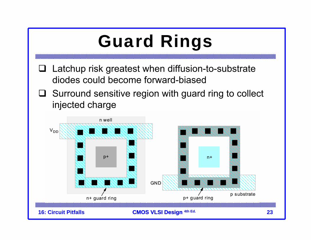
Guard RingsLatchup risk greatest when diffusion-to-substrate diodes could become forward-biasedSurround sensitive region with guard ring to collect injected charge
16: Circuit Pitfalls 24CMOS VLSI DesignCMOS VLSI Design 4th Ed.
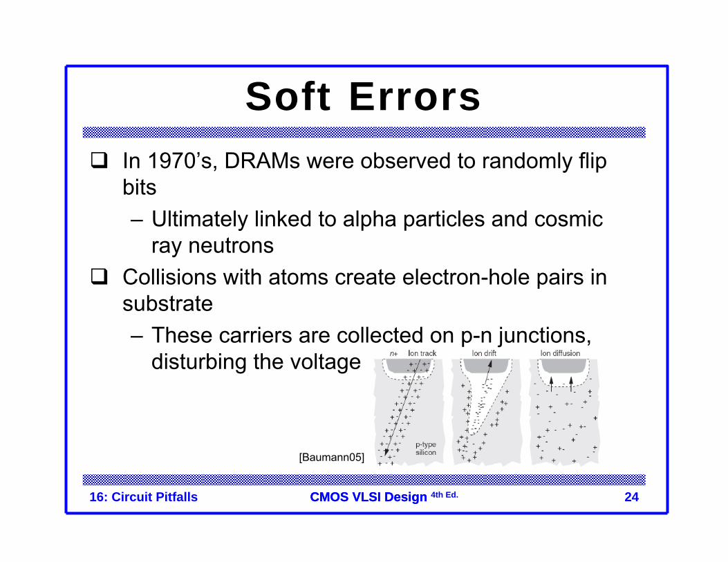
Soft ErrorsIn 1970’s, DRAMs were observed to randomly flip bits– Ultimately linked to alpha particles and cosmic
ray neutronsCollisions with atoms create electron-hole pairs in substrate– These carriers are collected on p-n junctions,
disturbing the voltage
[Baumann05]
16: Circuit Pitfalls 25CMOS VLSI DesignCMOS VLSI Design 4th Ed.
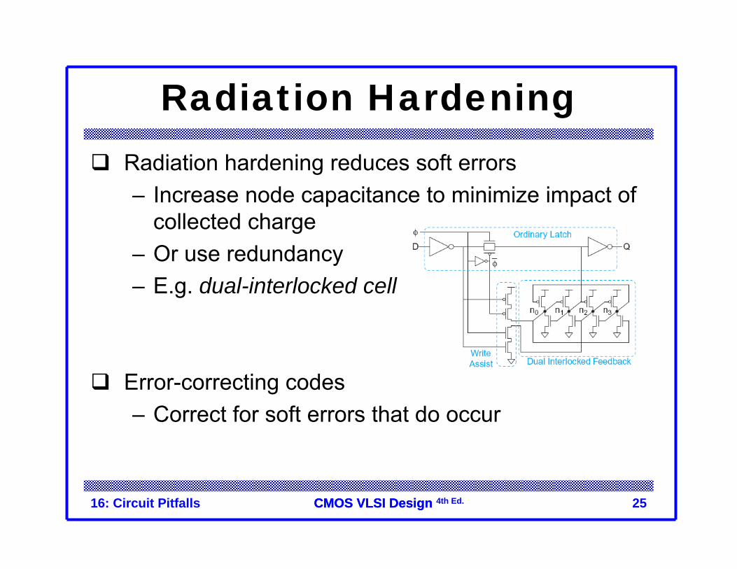
Radiation HardeningRadiation hardening reduces soft errors– Increase node capacitance to minimize impact of
collected charge– Or use redundancy– E.g. dual-interlocked cell
Error-correcting codes– Correct for soft errors that do occur
16: Circuit Pitfalls 26CMOS VLSI DesignCMOS VLSI Design 4th Ed.
Circuit PitfallsDetective puzzle– Given circuit and symptom, diagnose cause and
recommend solution– All these pitfalls have caused failures in real chips
16: Circuit Pitfalls 27CMOS VLSI DesignCMOS VLSI Design 4th Ed.
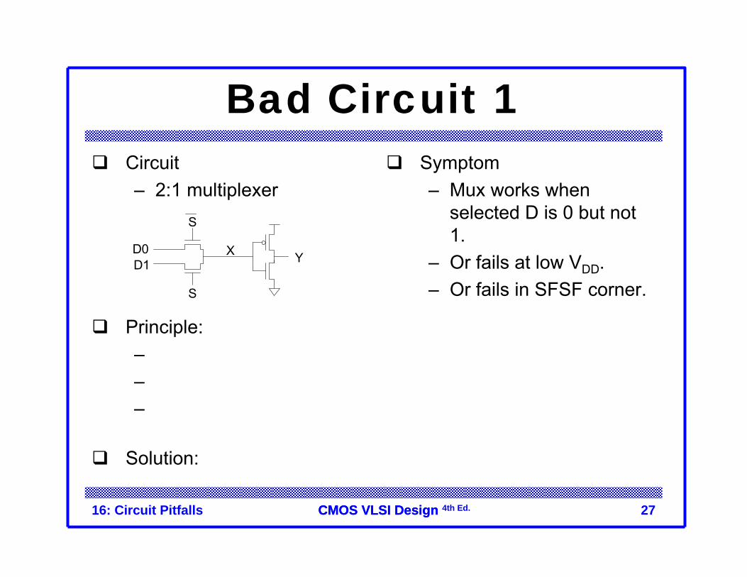
Bad Circuit 1Circuit– 2:1 multiplexer
Symptom– Mux works when
selected D is 0 but not 1.
– Or fails at low VDD.– Or fails in SFSF corner.
XD0YD1
S
S
Principle: Threshold drop– X never rises above VDD-Vt
– Vt is raised by the body effect– The threshold drop is most serious as Vt becomes a greater
fraction of VDD.Solution: Use transmission gates, not pass transistors
16: Circuit Pitfalls 28CMOS VLSI DesignCMOS VLSI Design 4th Ed.
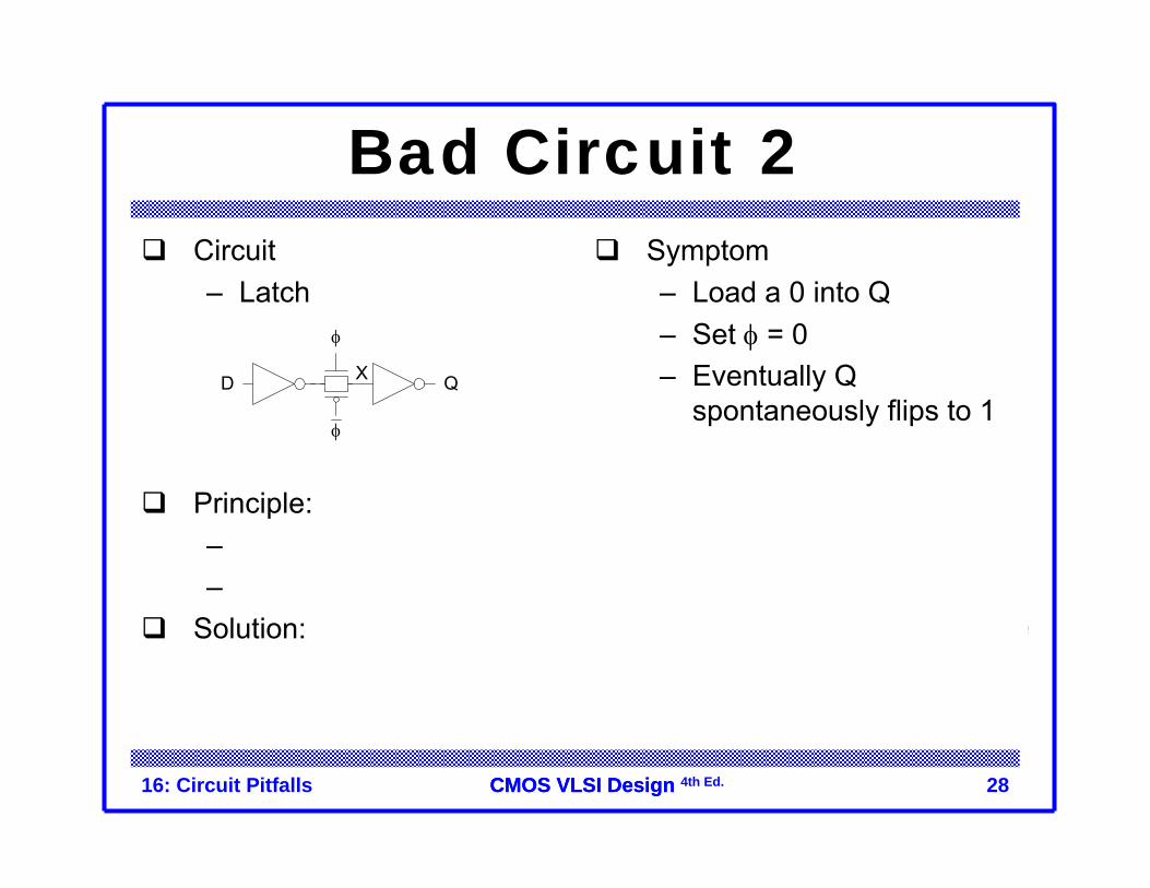
Bad Circuit 2Circuit– Latch
Symptom– Load a 0 into Q– Set φ = 0– Eventually Q
spontaneously flips to 1
Principle: Leakage– X is a dynamic node holding value as charge on the node– Eventually subthreshold leakage may disturb charge
Solution: Staticize node with feedback– Or periodically refresh node (requires fast clock,
not practical processes with big leakage)
D Q
φ
φ
X
φ
φ
Q
D X
φ
φ
16: Circuit Pitfalls 29CMOS VLSI DesignCMOS VLSI Design 4th Ed.
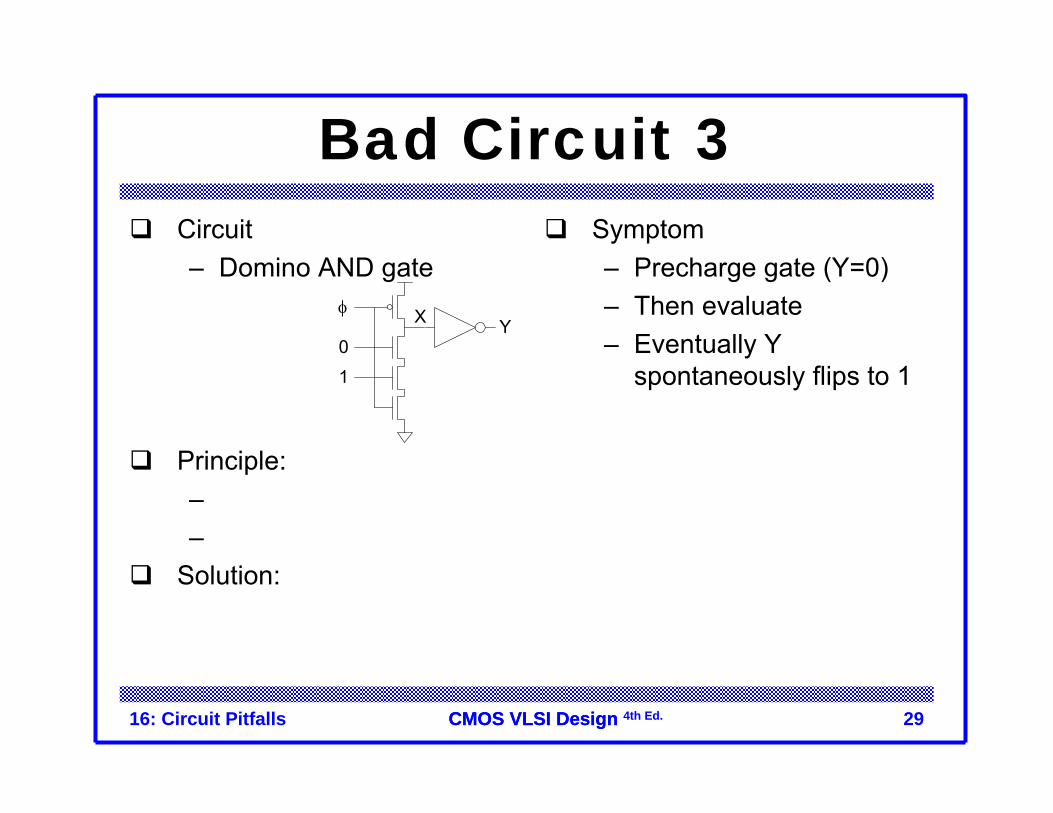
Bad Circuit 3Circuit– Domino AND gate
Symptom– Precharge gate (Y=0)– Then evaluate– Eventually Y
spontaneously flips to 1
Principle: Leakage– X is a dynamic node holding value as charge on the node– Eventually subthreshold leakage may disturb charge
Solution: Keeper
1
0Y
φ X
1
0Y
φ
X
16: Circuit Pitfalls 30CMOS VLSI DesignCMOS VLSI Design 4th Ed.
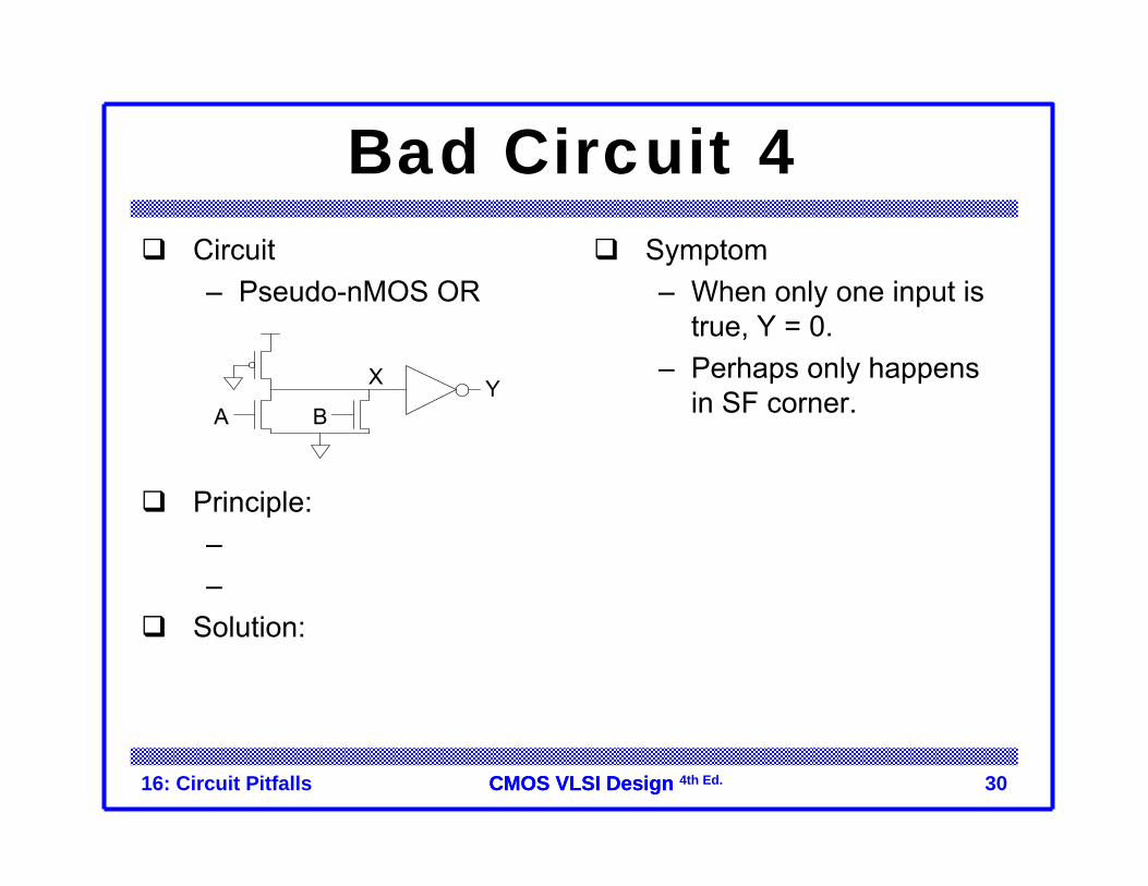
Bad Circuit 4Circuit– Pseudo-nMOS OR
Symptom– When only one input is
true, Y = 0.– Perhaps only happens
in SF corner.
Principle: Ratio Failure– nMOS and pMOS fight each other.– If the pMOS is too strong, nMOS cannot pull X low enough.
Solution: Check that ratio is satisfied in all corners
A BYX
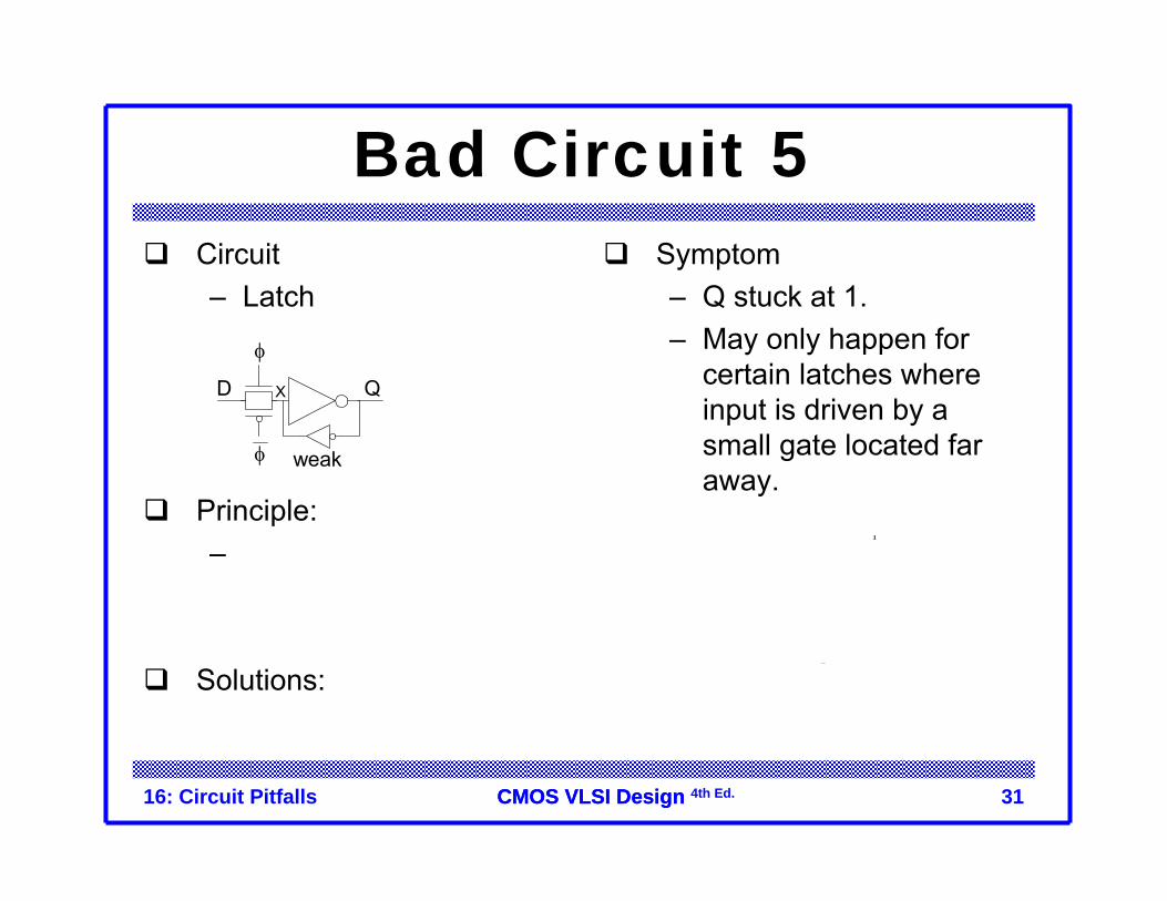
16: Circuit Pitfalls 31CMOS VLSI DesignCMOS VLSI Design 4th Ed.
Bad Circuit 5Circuit– Latch
Symptom– Q stuck at 1.– May only happen for
certain latches where input is driven by a small gate located far away.
Principle: Ratio Failure (again)– Series resistance of D driver, wire
resistance, and tgate must be much less than weak feedback inverter.
Solutions: Check relative strengths– Avoid unbuffered diffusion inputs where driver is unknown
QD
φ
φ weak
X
QD
φ
φ weakstronger
16: Circuit Pitfalls 32CMOS VLSI DesignCMOS VLSI Design 4th Ed.
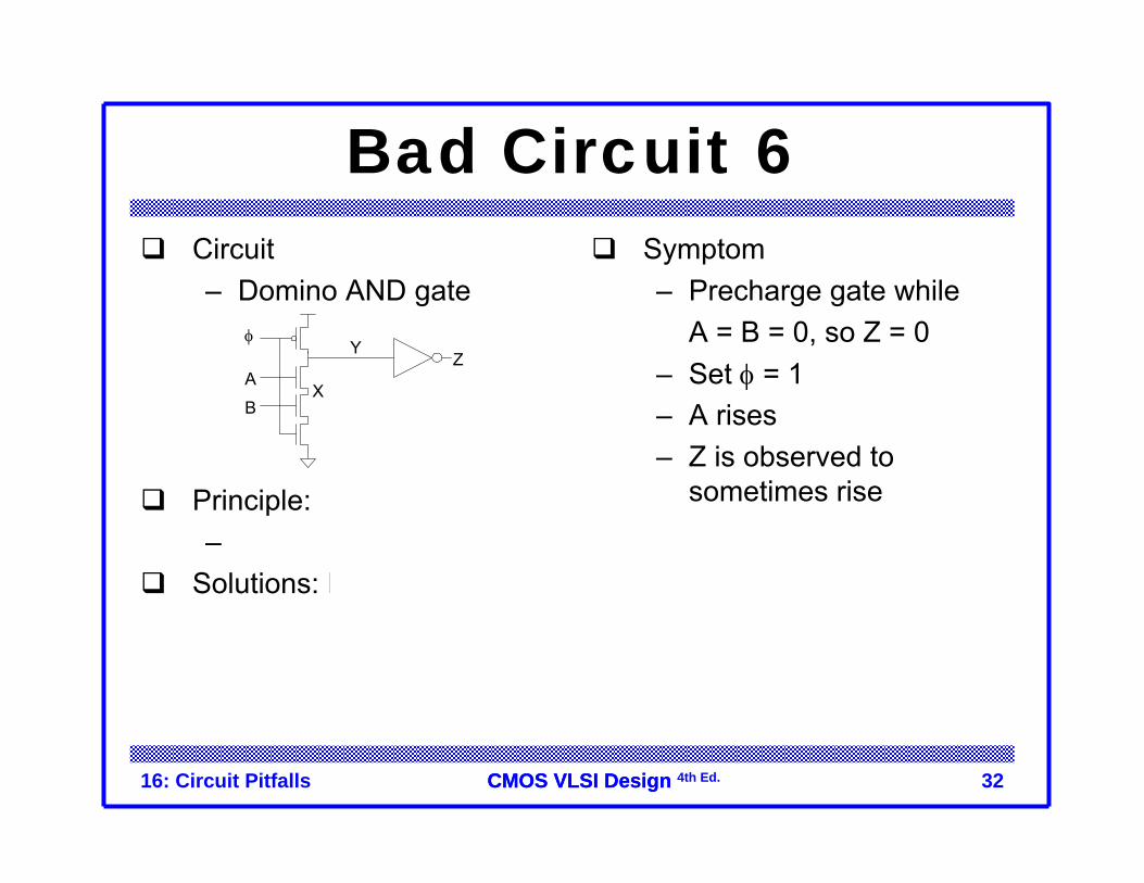
Bad Circuit 6Circuit– Domino AND gate
Symptom– Precharge gate while
A = B = 0, so Z = 0– Set φ = 1– A rises– Z is observed to
sometimes risePrinciple: Charge Sharing– If X was low, it shares charge with Y
Solutions: Limit charge sharing
– Safe if CY >> CX
– Or precharge node X too
B
A
Yφ
X
Z
B
A
Yφ
X
Cx
CY
ZYx Y DD
x Y
CV V VC C
= =+
16: Circuit Pitfalls 33CMOS VLSI DesignCMOS VLSI Design 4th Ed.
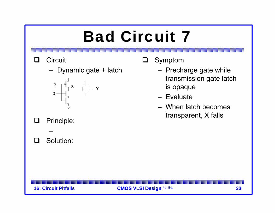
Bad Circuit 7Circuit– Dynamic gate + latch
Symptom– Precharge gate while
transmission gate latch is opaque
– Evaluate– When latch becomes
transparent, X fallsPrinciple: Charge Sharing– If Y was low, it shares charge with X
Solution: Buffer dynamic nodes before driving transmission gate
0
XφY
16: Circuit Pitfalls 34CMOS VLSI DesignCMOS VLSI Design 4th Ed.
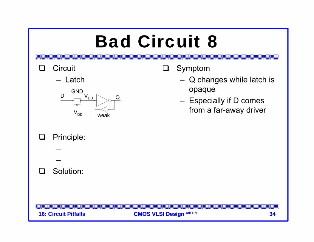
Bad Circuit 8Circuit– Latch
Symptom– Q changes while latch is
opaque– Especially if D comes
from a far-away driver
Principle: Diffusion Input Noise Sensitivity– If D < -Vt, transmission gate turns on– Most likely because of power supply noise or coupling on D
Solution: Buffer D locally
QD
weakVDD
VDD
GND
QD
0
weakVDD
VDD
16: Circuit Pitfalls 35CMOS VLSI DesignCMOS VLSI Design 4th Ed.
SummaryStatic CMOS gates are very robust– Will settle to correct value if you wait long enough
Other circuits suffer from a variety of pitfalls– Tradeoff between performance & robustness
Essential to check circuits for pitfalls– For large chips, you need an automatic checker.– Design rules aren’t worth the paper they are
printed on unless you back them up with a tool.
Related Documents