Lecture 15 • Advanced Technology Platforms – Background and Trends – State-of-the-Art CMOS Platforms Reading: multiple research articles (reference list at the end of this lecture)

Welcome message from author
This document is posted to help you gain knowledge. Please leave a comment to let me know what you think about it! Share it to your friends and learn new things together.
Transcript
Lecture 15• Advanced Technology Platforms
– Background and Trends– State-of-the-Art CMOS Platforms
Reading: multiple research articles (referencelist at the end of this lecture)

Technology and Applications
11/24/2013 2Nuo Xu EE 290D, Fall 2013

http://www.slideshare.net/kleinerperkins/kpcb‐top‐10‐mobile‐trends‐feb‐2011 3http://www.slideshare.net/kleinerperkins/kpcb-top-10-mobile-trends-feb-2011
Evolution of the Mainstream Computing Media
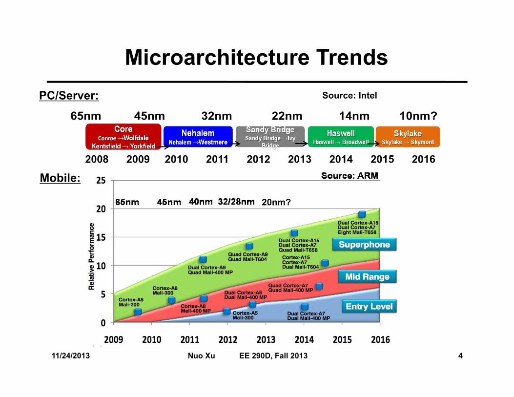
Microarchitecture Trends
11/24/2013 4Nuo Xu EE 290D, Fall 2013
Mobile:
PC/Server:
20nm?
Source: Intel
2008 2009 2010 2011 2012 2013 2014 2015 2016
65nm 45nm 32nm 22nm 14nm 10nm?

State-of-the-Art MPUs
11/24/2013 5Nuo Xu EE 290D, Fall 2013
Mobile:
Server: PC:
A6 ARMv7 32nm Samsung 1.3 GHz
A7 ARMv8a 28nm Samsung 1.8 GHz
Tegra 4 Cortex A15 28nm HPL TSMC
Tegra 4i Cortex A9 32nm LP Samsung 1.7 GHz
Snapdragon 800
Krait 400 28nm LP TSMC 1.9 GHz
Snapdragon600
Krait 300 28nm HPM TSMC 2.3 GHz
Exynos 5 Octa(5410)
Cortex A15 28nm LP Samsung 1.8 GHz
Exynos 4Quad (4412)
Cortex A7 32nm LP Samsung 1.6 GHz
Processor Architecture Technology Foundry Frequency
Xeon E5 Ivy Bridge 22nm TriGate
Intel 2.5-3.6 GHz
Core i7 1.8-3.0 GHz
Opteron 4200 Piledriver 32nm PDSOI
Global-foundries
1.8-3.3 GHz
FX-8350 2.9-4.2 GHz
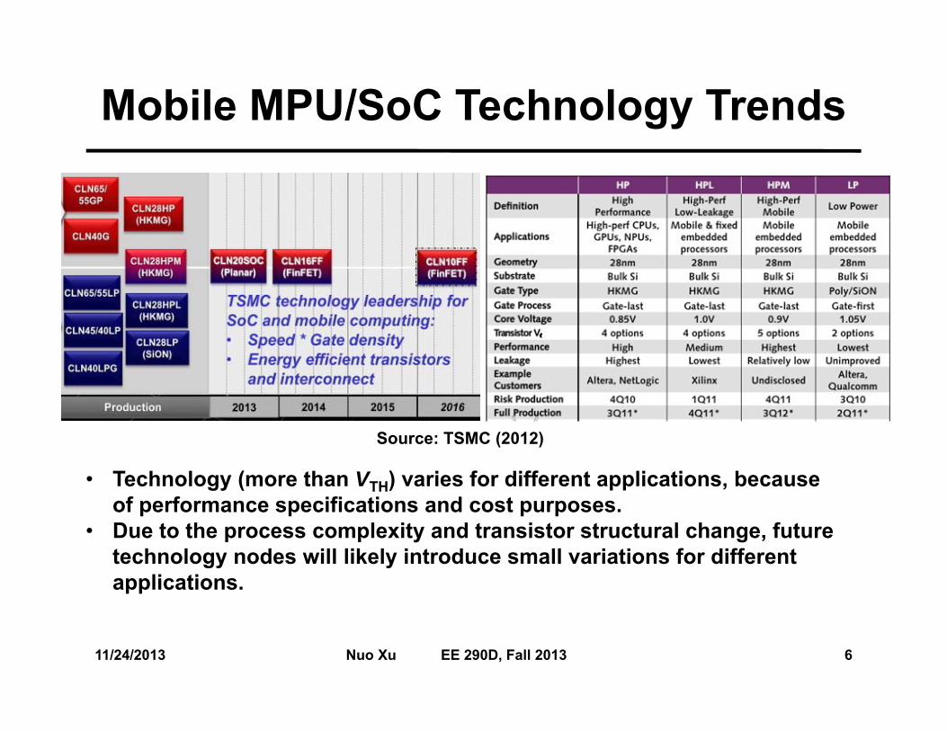
Mobile MPU/SoC Technology Trends
Source: TSMC (2012)
• Technology (more than VTH) varies for different applications, because of performance specifications and cost purposes.
• Due to the process complexity and transistor structural change, future technology nodes will likely introduce small variations for different applications.
11/24/2013 6Nuo Xu EE 290D, Fall 2013

90nm Platforms
11/24/2013 7Nuo Xu EE 290D, Fall 2013
• Structure: planar bulk• Strained-Si technology: eSiGe for PMOS; sCESL for NMOS• VDD = 1.2V; Lg,NMOS = 45nm; Lg,PMOS = 50nm
NMOS XTEM PMOS XTEM Process Flow
Short Channel Effect IOFF vs. ION plots
PMOSNMOS
PMOS
NMOS
T. Ghani, IEDM (2003)

65nm Platforms
11/24/2013 8Nuo Xu EE 290D, Fall 2013
NMOS XTEM PMOS XTEM Mobility Enhancement
NMOS PMOS
90 nm90 nm
65 nm 65 nm
Delay vs. Tech. Gen.
~ 0.73x
Layout Dependent Stress
Architecture Innovation
• Lg = 35nm• Dual-Poly/SiON process
S. Tyagi, IEDM (2005)

45nm Platforms
11/24/2013 9Nuo Xu EE 290D, Fall 2013
• Strained-Si technology: eSiGe for PMOS; SMT for NMOS• High-κ First + Metal Gate Last• VDD = 1.0V; Lg,HP = 35nm; Lg,LP = 45nm
IOFF vs. ION plotsPerf. Improvement over 65nm
NMOS XTEM PMOS XTEM TCAD Simulation of PMOS Sxx
SiGe SiGe
Tensile Contact & Compressive Gate Stress on NMOS
C. Auth, VLSI-T (2008)C.-H. Jan, IEDM (2008)

32nm Platforms
11/24/2013 10Nuo Xu EE 290D, Fall 2013
• Raised Source/Drain• High- κ + Metal Gate Last• Lg,HP = 36nm, the performance benefit by
reducing Lg stops from this node.P. Packan, IEDM (2009)
XTEMs
IOFF vs. Idlin plots
• Gate pitch scaling can continue for some generations…

28nm Foundry Platforms
11/24/2013 11Nuo Xu EE 290D, Fall 2013 C.W. Liang, VLSI-T (2011)
6T SRAM SEM SNM & VDDmin
SiGe SiGe
IOFF vs. ION plotsProcess Flow PMOS XTEM
• Poly Si/SiON gate stack→ EOTelec = 1.93nm
• tCESL+SMT for NMOS; eSiGe for PMOS
• VDD = 1.0/0.7V• Cu/Ultra Low-κ (2.5)/11 MLs
for BEOL• w/o HKMG → Low Cost +
High Yield
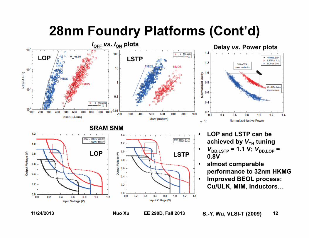
28nm Foundry Platforms (Cont’d)
11/24/2013 12Nuo Xu EE 290D, Fall 2013 S.-Y. Wu, VLSI-T (2009)
IOFF vs. ION plots
SRAM SNM
Delay vs. Power plots
LSTPLOP
• LOP and LSTP can be achieved by VTH tuning
• VDD,LSTP = 1.1 V; VDD,LOP = 0.8V
• almost comparable performance to 32nm HKMG
• Improved BEOL process: Cu/ULK, MIM, Inductors…
LSTPLOP
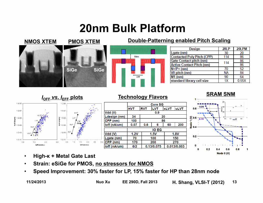
20nm Bulk Platform
• High-κ + Metal Gate Last• Strain: eSiGe for PMOS, no stressors for NMOS• Speed Improvement: 30% faster for LP, 15% faster for HP than 28nm node
11/24/2013 13Nuo Xu EE 290D, Fall 2013 H. Shang, VLSI-T (2012)
NMOS XTEM PMOS XTEM Double-Patterning enabled Pitch Scaling
SiGe SiGe
IOFF vs. IEFF plots Technology Flavors SRAM SNM

28nm UTBB FDSOI Platform
• 12nm-Si/25nm-BOX SOI wafer; Final tSOI=7nm• HKMG First, Tinv=1.5(1.65)nm• Doped GP, causing a splitting of 2 VTH (RVT, LVT);
Dynamic VTH by FBB/RBB?• No HALO doping• N(P)MOS: ION=1070(610)uA/um; IOFF=16(30)nA/um
DIBL=90-95mV; SS=85-90mV/dec @1V VDD
XTEM Pelgrom plots
Lg=40nm for SRAM
11/24/2013 14Nuo Xu EE 290D, Fall 2013
Back Biasing
IOFF vs. ION plots
N. Planes, VLSI-T (2012)
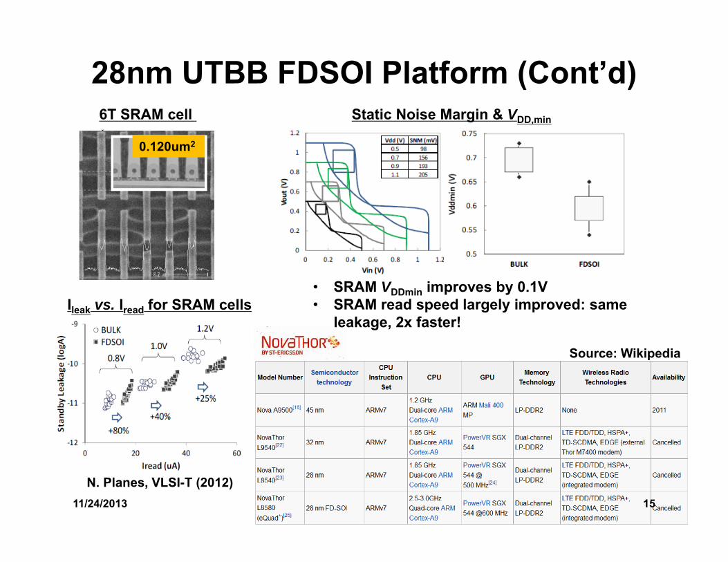
28nm UTBB FDSOI Platform (Cont’d)
Ileak vs. Iread for SRAM cells
6T SRAM cell
0.120um2
• SRAM VDDmin improves by 0.1V• SRAM read speed largely improved: same
leakage, 2x faster!
11/24/2013 15
Static Noise Margin & VDD,min
Source: Wikipedia
N. Planes, VLSI-T (2012)

20nm UTBB FDSOI?
• 20nm FDSOI development goal: 30% performance boost over bulk referenceThis comes from: 8-12% parasite capacitance; 4-6% SS and 8-10% IEFF improvement.
• Biggest difference compared to ST’s 28nm FD: Low VTH FDSOI-PFET uses 27%Ge-SiGe channel, (epi SiGe on top of SOI, then
oxidize) → a VTH lowering of 200mV can be achieved. BOX thickness reduces from 25nm to 20nm. NFET: in-situ P-doped S&D; No LDD, pocket, HALO, HDD implants used
NFET and PFET Current EnhancementChemical analysis of 20nm FD-PFET
20nm FD process wrt 20nm bulk process
M. Haond, Int SOI Conf. (2012)11/24/2013 16Nuo Xu EE 290D, Fall 2013
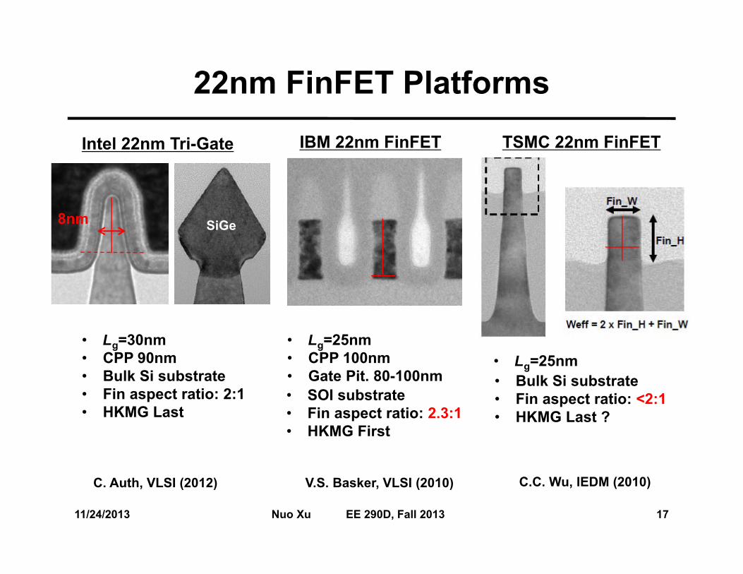
22nm FinFET Platforms
Intel 22nm Tri-Gate IBM 22nm FinFET TSMC 22nm FinFET
C.C. Wu, IEDM (2010)
• Lg=25nm• CPP 100nm• Gate Pit. 80-100nm
• Lg=25nm
• SOI substrate• Fin aspect ratio: 2.3:1• HKMG First
• Bulk Si substrate• Fin aspect ratio: <2:1• HKMG Last ?
C. Auth, VLSI (2012)
8nm
• Lg=30nm• CPP 90nm• Bulk Si substrate• Fin aspect ratio: 2:1• HKMG Last
11/24/2013 17Nuo Xu EE 290D, Fall 2013
V.S. Basker, VLSI (2010)
SiGe

22nm FinFET Performance
Intel 22nm Tri-Gate IBM 22nm FinFET TSMC 22nm FinFET
N: 1.2mA/umP: 1.1mA/um
N: 1.2mA/umP: 950uA/um
VLSI 2010
VLSI 2011 IEDM 2010
IEDM 2009
@IOFF of 100nA/um
@ 1V VDD @ 1V VDD18
N: 1.26mA/umP: 1.10mA/um
@ 0.8V VDD
VLSI 2012
PMOS
NMOS

22nm Bulk FinFET: to Probe Further
• Almost idea electrostatics: N(P) FET DIBL=46(50) mV/V; SS=69(72) mV/dec; @0.8V VDD
• Threshold voltage engineering by tuning Lg + doping• 193nm Immersion litho. to achieve 8nm Fin width, corner rounding (3.5nm radius)• 5th-gen strained-Si tech: Si0.5Ge0.5 S/D + Gate-Last for PFET; “some technique” for
NFET• Misalignment at CESL to form contacts; contact wrap around the fin• 9-layer Cu interconnect; MIM introduced between M8 & M9
NMOS PBTI Improvement
Misaligned-Contacts to avoid Gate/SD Shorting
11/24/2013 19Nuo Xu EE 290D, Fall 2013C. Auth, VLSI-T (2012)C.-H. Jan, IEDM (2012)
Technology Flavors
I/O Devices
Short-Channel Effect

Improvement over 32nm Planar Platforms
11/24/2013 20Nuo Xu EE 290D, Fall 2013
C.-H. Jan, IEDM (2012)K. Kuhn, IEDM (2012)
Delay vs. Power plotsPMOS IEFF Improvement
SRAM Power & Intrinsic Gain Improvement• As compared to precedent
planar platforms, most of the performance enhancement comes from electrostatics improvement!

References1. (Intel 90nm) K. Mistry et al., “Delaying Forever: Uniaxial Strained Silicon Transistors in a 90nm
CMOS Technology,” Symposium on VLSI Technology Dig., pp.50-51, 2004.2. (Intel 65nm) S. Tyagi et al., “An Advanced Low Power, High Performance, Strained Channel 65nm
Technology,” IEEE International Electron Devices Meeting Tech. Dig., pp.1070-1072, 2005.3. (Intel 45nm) C. Auth et al., “45nm High-k+Metal Gate Strain-Enhanced Transistors,” Symposium
on VLSI Technology Dig., pp.128-129, 2008.4. (Intel 32nm) P. Packan et al., “High Performance 32nm Logic Technology Featuring 2nd Generation
High-k + Metal Gate Transistors,” IEEE International Electron Devices Meeting Tech. Dig., pp.659-662, 2009.
5. (UMC 28nm) C.W. Liang et al., “A 28nm Poly/SiON CMOS Technology for Low Power SoCApplications,” Symposium on VLSI Technology Dig., pp.38-39, 2011.
6. (TSMC 28nm) S.-Y. Wu et al., “A Highly Manufacturable 28nm CMOS Low Power PlatformTechnology with Fully Functional 64Mb SRAM Using Dual/Triple Gate Oxide Process,”Symposium on VLSI Technology Digest, pp.210-211, 2009.
7. (IBM 20nm Bulk) H. Shang et al., “High Performance Bulk Planar 20nm CMOS Technology forLow Power Mobile Applications,” Symposium on VLSI Technology Digest, pp. 129-130, 2012.
8. (ST 28nm FDSOI) N. Planes et al., “28nm FDSOI Technology Platform for High-Speed Low-Voltage Digital Applications,” Symp. VLSI Tech. Dig., pp. 133-134, 2012.
9. (ST 20nm FDSOI) M. Haond et al., “20 nm FDSOI Process and Design Platforms for HighPerformance/Low Power Systems on Chip,” IEEE International SOI Conference, 2012.
10. (Intel 22nm Fin) C. Auth et al., “A 22nm High Performance and Low-Power CMOS TechnologyFeaturing Fully-Depleted Tri-Gate Transistors, Self-Aligned Contacts and High Density MIMCapacitors,” Symposium on VLSI Technology Dig., pp. 131-132, 2012.
References11. C.-H. Jan et al., “A 22nm SoC Platform Technology Featuring 3-D Tri-Gate and High-k/Metal Gate,
Optimized for Ultra Low Power, High Performance and High Density SoC Applications,” IEEEInternational Electron Device Meeting Tech. Dig., pp.44-47, 2012.
12. K. Kuhn et al., “The Ultimate CMOS Device and Beyond,” IEEE International Electron DeviceMeeting Tech. Dig., pp. 171-174, 2012.
13. (IBM 22nm Fin) V.S. Basker et al., “A 0.063um2 FinFET SRAM Cell Demonstration withConventional Lithography using a Novel Integration Scheme with Aggressively Scaled Fin andGate Pitch,” Symposium on VLSI Technology Dig., pp.19-20, 2010.
14. (TSMC 22nm Fin) C.C. Wu et al., “High Performance 22/20nm FinFET CMOS Devices withAdvanced High-/Metal Gate Scheme,” IEEE International Electron Device Meeting Tech. Dig.,pp.600-603, 2010.
Related Documents