EE130 Lecture 15, Slide 1 Spring 2003 Lecture #15 OUTLINE The Bipolar Junction Transistor – Fundamentals – Ideal Transistor Analysis Reading: Chapter 10, 11.1 EE130 Lecture 15, Slide 2 Spring 2003 Bipolar Junction Transistors (BJTs) • Over the past 3 decades, the higher layout density and low-power advantage of CMOS technology has eroded away the BJT’s dominance in integrated-circuit products. (higher circuit density better system performance) • BJTs are still preferred in some digital-circuit and analog-circuit applications because of their high speed and superior gain. faster circuit speed larger power dissipation limits integration level to ~10 4 circuits/chip

Welcome message from author
This document is posted to help you gain knowledge. Please leave a comment to let me know what you think about it! Share it to your friends and learn new things together.
Transcript
1
EE130 Lecture 15, Slide 1Spring 2003
Lecture #15
OUTLINE
The Bipolar Junction Transistor– Fundamentals
– Ideal Transistor Analysis
Reading: Chapter 10, 11.1
EE130 Lecture 15, Slide 2Spring 2003
Bipolar Junction Transistors (BJTs)• Over the past 3 decades, the higher layout density and
low-power advantage of CMOS technology has eroded away the BJT’s dominance in integrated-circuit products.
(higher circuit density better system performance)
• BJTs are still preferred in some digital-circuit and analog-circuit applications because of their high speed and superior gain.
faster circuit speedlarger power dissipation
limits integration level to ~104 circuits/chip

2
EE130 Lecture 15, Slide 3Spring 2003
Introduction• The BJT is a 3-terminal device
– 2 types: PNP and NPN
VEB = VE – VBVCB = VC – VBVEC = VE – VC
= VEB - VCB
VBE = VB – VEVBC = VB – VCVCE = VC – VE
= VCB - VEB
• The convention used in the textbook does not follow IEEE convention (currents defined as positive flowing into a terminal)
• We will follow the convention used in the textbook
EE130 Lecture 15, Slide 4Spring 2003
Charge Transport in a BJT• Consider a reverse-biased pn junction:
– Reverse saturation current depends on rate of minority-carrier generation near the junction⇒ can increase reverse current by increasing rate of
minority-carrier generation:Optical excitation of carriers
Electrical injection of minority carriers into the neighborhood of the junction
3
EE130 Lecture 15, Slide 5Spring 2003
ICp
ICn
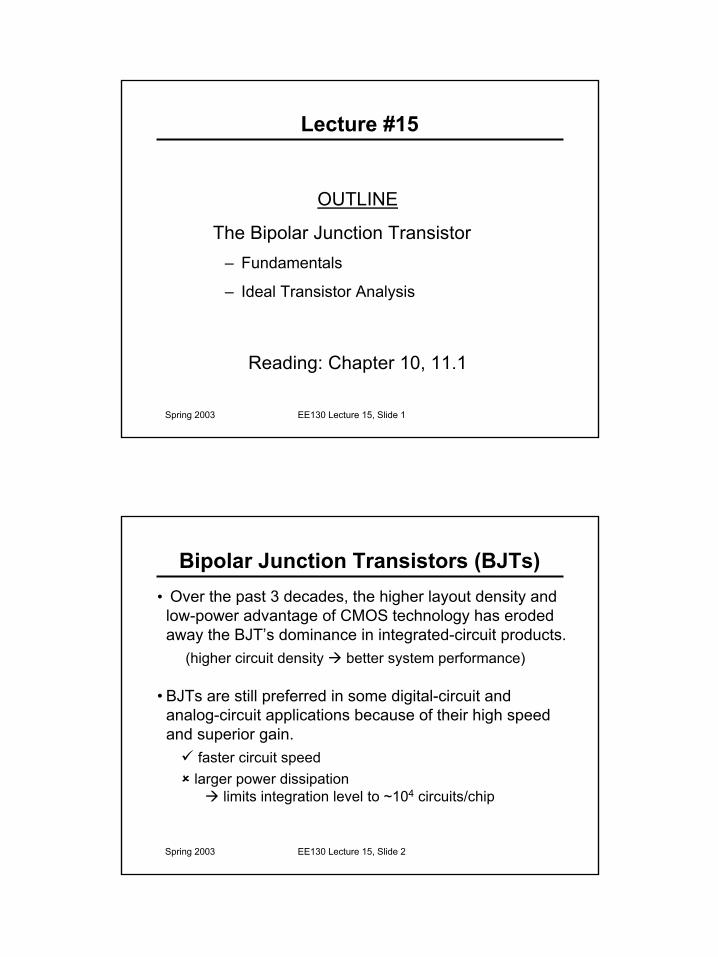
PNP BJT Operation (Qualitative)
B
Cdc I
I≅β
“Active Bias”: VEB > 0 (forward bias), VCB < 0 (reverse bias)
“Emitter”
“Base”
“Collector”
EE130 Lecture 15, Slide 6Spring 2003
• Important features of a good transistor:– Injected minority carriers do not recombine in the
neutral base region
– Emitter current is comprised almost entirely of carriers injected into the base (rather than carriers injected into the emitter
BJT Design
4
EE130 Lecture 15, Slide 7Spring 2003
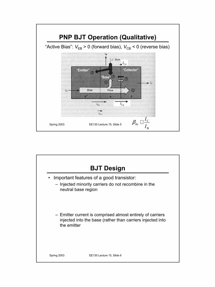
The base current consists of majority carriers supplied for1. Recombination of injected minority carriers in the base2. Injection of carriers into the emitter3. Reverse saturation current in collector junction
• Reduces | IB |4. Recombination in the base-emitter depletion region
Base Current Components
EE130 Lecture 15, Slide 8Spring 2003
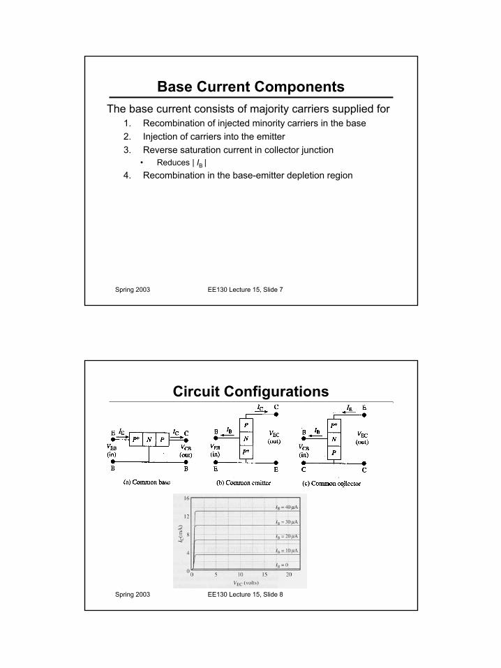
Circuit Configurations

5
EE130 Lecture 15, Slide 9Spring 2003
Modes of OperationCommon-emitter output characteristics
(IC vs. VCE)
EE130 Lecture 15, Slide 10Spring 2003
BJT Electrostatics• Under normal operating conditions, the BJT may be
viewed electrostatically as two independent pn junctions

6
EE130 Lecture 15, Slide 11Spring 2003
• Emitter Efficiency:
– Decrease (5) relative to (1+2)to increase efficiency
• Base Transport Factor:
– Decrease (1) relative to (2)to increase transport factor
BJT Performance Parameters (PNP)
EnEp
Ep
III+=γ
Ep
Cp
T II=α
Tdc γαα ≡• Common-Base d.c. Current Gain:
EE130 Lecture 15, Slide 12Spring 2003
Collector Current (PNP)• The collector current is comprised of
• Holes injected from emitter, which do not recombine in the base ← (2)
• Reverse saturation current of collector junction ← (3)
where ICB0 is the collector current which flows when IE = 0
( )
0
0
0
α1α1
αα
CEB
dc
CBB
dc
dcC
CBBCdcC
IβI
III
IIII
+=−
+−
=
++=
0α CBEdcC III +=
• Common-Emitter d.c. Current Gain:
dc
dc1dc ααβ −=
7
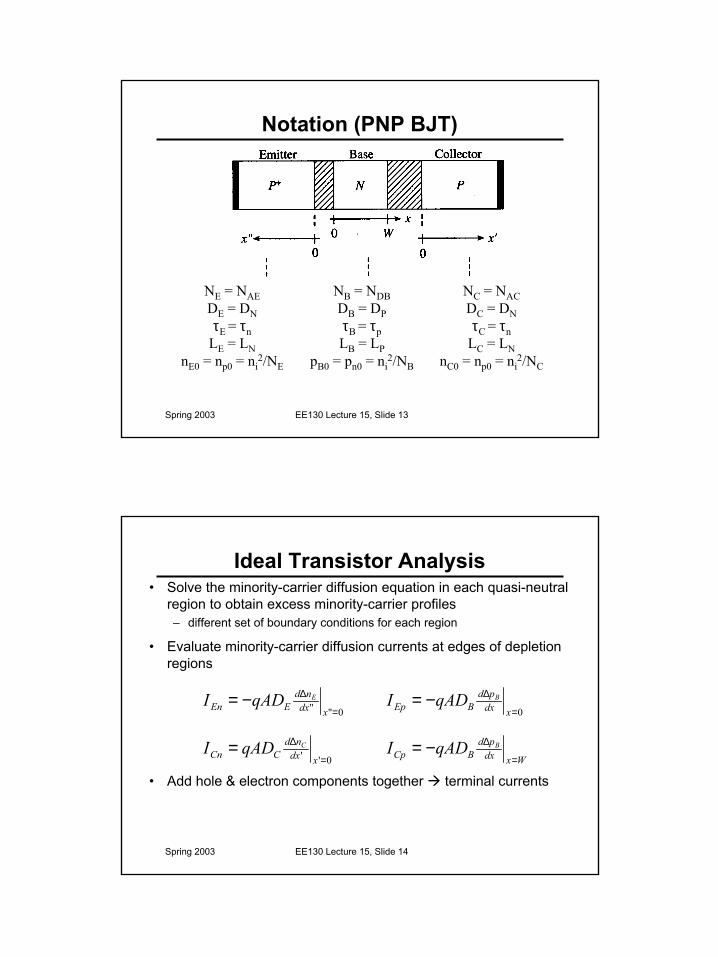
EE130 Lecture 15, Slide 13Spring 2003
Notation (PNP BJT)
NE = NAEDE = DNτE = τn
LE = LNnE0 = np0 = ni
2/NE
NB = NDBDB = DPτB = τpLB = LP
pB0 = pn0 = ni2/NB
NC = NACDC = DNτC = τn
LC = LNnC0 = np0 = ni
2/NC
EE130 Lecture 15, Slide 14Spring 2003
Ideal Transistor Analysis• Solve the minority-carrier diffusion equation in each quasi-neutral
region to obtain excess minority-carrier profiles– different set of boundary conditions for each region
• Evaluate minority-carrier diffusion currents at edges of depletion regions
• Add hole & electron components together terminal currents
0"" =
∆−=xdx
ndEEn
EqADI0=
∆−=xdx
pdBEp
BqADI
Wxdxpd
BCpBqADI
=
∆−=0'' =
∆=xdx
ndCCn
CqADI

8
EE130 Lecture 15, Slide 15Spring 2003
Emitter Region Formulation• Diffusion equation:
• Boundary Conditions:
E
EE ndxnd
ED τ∆∆ −= 2
2
"0
)1()0"(
0)"(/
0 −==∆
=∞→∆kTqV
EE
E
EBenxn
xn
EE130 Lecture 15, Slide 16Spring 2003
Base Region Formulation• Diffusion equation:
• Boundary Conditions:
B
BB pdxpd
BD τ∆∆ −= 2
2
0
)1()(
)1()0(/
0
/0
−=∆
−=∆kTqV
BB
kTqVBB
CB
EB
epWp
epp

9
EE130 Lecture 15, Slide 17Spring 2003
Collector Region Formulation• Diffusion equation:
• Boundary Conditions:
C
CC ndxnd
CD τ∆∆ −= 2
2
'0
)1()0'(
0)'(/
0 −==∆
=∞→∆kTqV
CC
C
CBenxn
xn
EE130 Lecture 15, Slide 18Spring 2003
Current Formulation
0"" =
∆−=xdx
ndEEn
EqADI
0=
∆−=xdx
pdBEp
BqADI
Wxdxpd
BCpBqADI
=
∆−=
0'' =
∆=xdx
ndCCn
CqADI
10
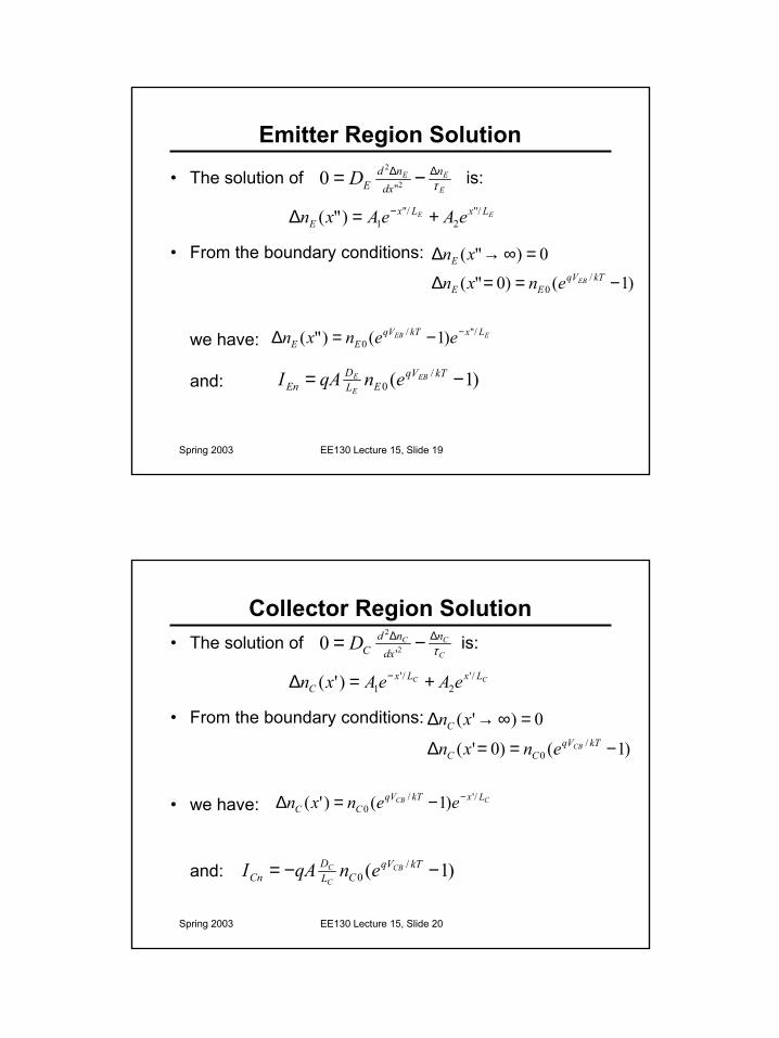
EE130 Lecture 15, Slide 19Spring 2003
Emitter Region Solution• The solution of is:
• From the boundary conditions:
we have:
and:
E
EE ndxnd
ED τ∆∆ −= 2
2
"0
EE LxLxE eAeAxn /"
2/"
1)"( +=∆ −
)1()0"(
0)"(/
0 −==∆
=∞→∆kTqV
EE
E
EBenxn
xn
EEB LxkTqVEE eenxn /"/
0 )1()"( −−=∆
)1( /0 −= kTqVEL
DEn
EB
E
E enqAI
EE130 Lecture 15, Slide 20Spring 2003
Collector Region Solution• The solution of is:
• From the boundary conditions:
• we have:
and:
CC LxLxC eAeAxn /'
2/'
1)'( +=∆ −
CCB LxkTqVCC eenxn /'/
0 )1()'( −−=∆
)1( /0 −−= kTqV
CLD
CnCB
C
C enqAI
C
CC ndxnd
CD τ∆∆ −= 2
2
'0
)1()0'(
0)'(/
0 −==∆
=∞→∆kTqV
CC
C
CBenxn
xn
11
EE130 Lecture 15, Slide 21Spring 2003
Base Region Solution• The solution of is:
• From the boundary conditions:
we have:
BB LxLxB eAeAxp /
2/
1)( +=∆ −
B
BB pdxnd
BD τ∆∆ −= 2
2
0
)1()(
)1()0(/
0
/0
−=∆
−=∆kTqV
BB
kTqVBB
CB
EB
epWp
epp
( )( )BLWBLW
BLxBLxCB
BLWBLWBLxWBLxW
EB
eeeekTqV
B
eeeekTqV
BB
ep
epxp
//
//
//
/)(/)(
)1(
)1()(/
0
/0
−
−
−
−−−
−−
−−
−+
−=∆
EE130 Lecture 15, Slide 22Spring 2003
• Now, we know• Therefore, we can write:
as
( ) 2sinh ξξξ −−= ee
( )( )BLWBLW
BLxBLxCB
BLWBLWBLxWBLxW
EB
eeeekTqV
B
eeeekTqV
BB
ep
epxp
//
//
//
/)(/)(
)1(
)1()(/
0
/0
−
−
−
−−−
−−
−−
−+
−=∆
( )[ ]( )
[ ]( )
B
BCB
B
BEB
LW
Lx
kTqVB
LW
LxW
kTqVBB
ep
epxp
sinhsinh
)1(
sinhsinh
)1()(
/0
/0
−+
−=∆−

12
EE130 Lecture 15, Slide 23Spring 2003
• We know• Therefore, we have:
and:
( ) 2cosh ξξξ −+= ee
( )[ ]1)1( /)/sinh(
1/)/sinh(
/cosh(0
) −−−= kTqVLW
kTqVLWLW
BLD
EpCB
B
EB
B
B
B
B eepqAI
( )[ ]1)1( /)/sinh(
/cosh(/)/sinh(
10
) −−−= kTqVLWLWkTqV
LWBLD
CpCB
B
BEB
BB
B eepqAI
EE130 Lecture 15, Slide 24Spring 2003
Terminal Currents• We know:
• Therefore:
( )[ ]1)1( /)/sinh(
1/)/sinh(
/cosh(0
) −−−= kTqVLW
kTqVLWLW
BLD
EpCB
B
EB
B
B
B
B eepqAI
)1( /0 −= kTqVEL
DEn
EB
E
E enqAI
( )[ ]1)1( /)/sinh(
/cosh(/)/sinh(
10
) −−−= kTqVLWLWkTqV
LWBLD
CpCB
B
BEB
BB
B eepqAI
)1( /0 −−= kTqV
CLD
CnCB
C
C enqAI
( ) ( )( )[ ]1)1( /)/sinh(
10
/)/sinh(
/cosh(00
) −−−+= kTqVLWBL
DkTqVLWLW
BLD
ELD
ECB
BB
BEB
B
B
B
B
E
E epepnqAI
( ) ( )( )[ ]1)1( /)/sinh(
/cosh(00
/)/sinh(
10
) −+−−= kTqVLWLW
BLD
CLDkTqV
LWBLD
CCB
B
B
B
B
C
CEB
BB
B epnepqAI

13
EE130 Lecture 15, Slide 25Spring 2003
Simplification• In real BJTs, we make W << LB for high gain.
Then, since
we have:
( )( ) 1for 1cosh
1for sinh
2
2
<<+→
<<→
ξξ
ξξξξ
( )( )WxkTqV
B
WxkTqV
BB
CB
EB
ep
epxp
)1(
1)1()(/
0
/0
−+
−−≅∆
EE130 Lecture 15, Slide 26Spring 2003
Performance Parameters (Active Mode)
( )
( )
( )221
221
221
2
2
2
2
2
2
1
11
11
11
BEE
B
B
E
Bi
Ei
BEE
B
B
E
Bi
Ei
B
EE
B
B
E
Bi
Ei
LW
LW
NN
DD
n
dc
LW
LW
NN
DD
n
dc
LWT
LW
NN
DD
n
n
n
n
+=
++=
+=
+=
β
α
α
γ Assumptions: • emitter junction forward biased, collector junction reverse biased• W << LB
Related Documents