EE 371 Lecture 14 M Horowitz 1 Lecture 14 Design for Testability Computer Systems Laboratory Stanford University [email protected] Copyright © 2006 Ron Ho, Mark Horowitz EE 371 Lecture 14 M Horowitz 2 Testing Basics • Testing and debug in commercial systems have many parts – What do I do in my design for testability? – How do I actually debug a chip? – What do I do once I’ve debugged a chip? • Two rules always hold true in testing/debug – If you design a testability feature, you probably won’t need to use it • Corollary: If you omit a testability feature, you WILL need to use it – If you don’t test it, it won’t work, guaranteed

Welcome message from author
This document is posted to help you gain knowledge. Please leave a comment to let me know what you think about it! Share it to your friends and learn new things together.
Transcript

EE 371 Lecture 14M Horowitz 1
Lecture 14
Design for Testability
Computer Systems Laboratory
Stanford University
Copyright © 2006 Ron Ho, Mark Horowitz
EE 371 Lecture 14M Horowitz 2
Testing Basics
• Testing and debug in commercial systems have many parts– What do I do in my design for testability?
– How do I actually debug a chip?
– What do I do once I’ve debugged a chip?
• Two rules always hold true in testing/debug– If you design a testability feature, you probably won’t need to use it
• Corollary: If you omit a testability feature, you WILL need to use it
– If you don’t test it, it won’t work, guaranteed

EE 371 Lecture 14M Horowitz 3
Two Checks
• There are two basic forms of validation– Functional test: Does this chip design produce the correct results?
– Manufacturing test: Does this particular die work? Can I sell it?
• What’s the difference?– Functional test seeks logical correctness
• >1 year effort, up to 50 people, to ensure that the design is good
– Manufacturing test is done on each die prior to market release• Send your parts through a burn-in oven and a tester before selling them
• The distinction is in the testing, not in the problem– Ex: A circuit marginality (such as charge-sharing in a domino gate)
• Can show up in either functional or manufacture test
EE 371 Lecture 14M Horowitz 4
Testing Costs Are High
• Functional test consumes lots of people and lots of $$– “Architecture Validation” (AV) teams work for many years
• Write lots of RTL tests in parallel with the chip design effort
• Reuse RTL tests from prior projects (backwards compatibility helps!)
– First 12 months after silicon comes back from fab• Large team (50+) gathered specifically for debug, usually pulling shifts
• First “root-cause” a problem, then do “onion-peeling” to find “many-rats”
• Manufacture test constrains high-volume production flow– Must run as many tests as needed to identify frequency bins
• Including the “zero-frequency” bin for keychains
– Automated test equipment (ATE) can cost $1-10 million
EE 371 Lecture 14M Horowitz 5
The Stakes Are Higher
• Recall of a defective part can sink a company– Or at least cost a lot of money: Intel FDIV recall cost nearly $500M
• Not just CPUs: NHTSA 97V034.001 recall– Izuzu Trooper had a bad voltage regulator IC, nearly 120,000 cars
• Time-to-market, or time-to-money, pressures are paramount– Industry littered with “missed windows” (Intel LCoS, Sun Millenium)
• How long does it take to “root-cause” a problem? (from Ron Ho)– Bad test, or layout-vs-schematic error, on ATE: 2 person-weeks
– Marginal circuit with intermittent error, on ATE: 2 person-months
– Logic error, or any error seen only on a system: 2 person-years
EE 371 Lecture 14M Horowitz 6
Testability in Design
• Build a number of test and debug features at design time
• This can include “debug-friendly” layout– For wirebond parts, isolate important nodes near the top
– For face-down/C4 parts, isolate important node diffusions
• This can also include special circuit modifications or additions– Scan chains that connect all of your flops/latches
– Built-in self-test (BIST)
– Analog probe circuits
– Spare gates
• Focus on the circuit modifications and debugging circuit issues– Spent time in EE271 on logical/functional testing
EE 371 Lecture 14M Horowitz 7
Scan Chains
• Lots and lots of flops/latches in a high-end chip– 200,000 latches on 2nd gen Itanium (static + dynamic)
• Scan chains offer two benefits for these latches and flops– Observability: you can stop the chip and read out all their states
– Controllability: you can stop the chip and set all of their states
• Critical for debugging circuit issues too– They are your easiest “probe” points in the circuit
– Can trace back errors to see where they first appear• Great with simulator or when a part fails in some condition
– Even more useful with a flexible clock generator• Can stress certain clock cycles, and look at which bits fail
EE 371 Lecture 14M Horowitz 8
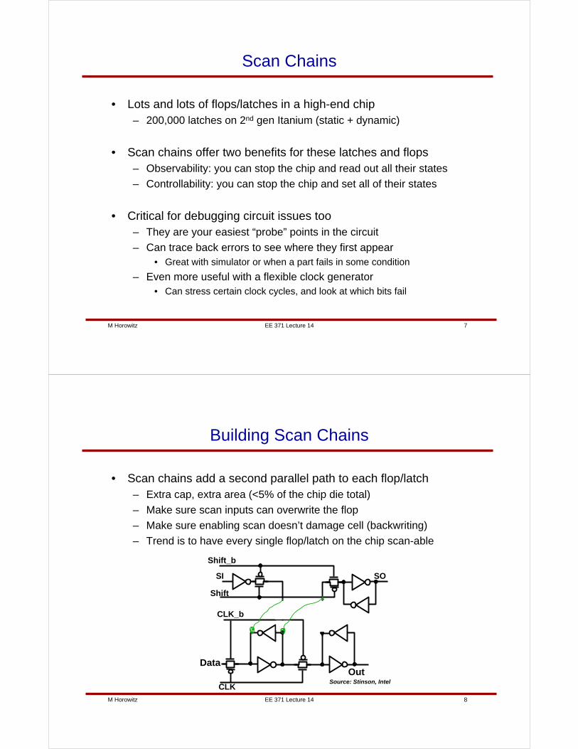
Building Scan Chains
• Scan chains add a second parallel path to each flop/latch– Extra cap, extra area (<5% of the chip die total)
– Make sure scan inputs can overwrite the flop
– Make sure enabling scan doesn’t damage cell (backwriting)
– Trend is to have every single flop/latch on the chip scan-able
CLK_b
CLK
OutData
SI SO
Shift
Shift_b
Source: Stinson, Intel

EE 371 Lecture 14M Horowitz 9
Other Scan Chains
• Previous scan flop had a dedicated shift in/out line– Can also share the outputs and clk– Simpler, but scanning out can “mess with” the rest of the chip
• Key: If nothing else works, make sure your scan chain does!– It is how you debug most everything on your chip
Flo
p
QD
CLK
SI
SCAN
scan out
scan-in
inputs outputs
Flo
pF
lop
Flo
pF
lop
Flo
pF
lop
Flo
pF
lop
Flo
pF
lop
Flo
pF
lop
LogicCloud
LogicCloud
Source: Harris, Addison-Wesley
EE 371 Lecture 14M Horowitz 10
Challenges with Scan, BIST, and ATPG
• Initialization states need to be clean – X’s corrupt signatures– Especially true for memory blocks; write to the array, then do test
• Logic can have “don’t care” states that the test may not realize
• Example: MUTEX– FF outputs cannot both be “1”
– But FFs are on the scan chain
– Scan can set up contention
– Tester sees “X” on the bus
• Must constrain ATPG/BIST
FF
FF
scan
EE 371 Lecture 14M Horowitz 11
Analog Test Facilities
• Scan/BIST facilities look at digital signals only– Sometimes analog signal levels are important to probe as well
– Clock, PLL filter cap voltage, low-swing signals, etc.
• We have a couple of tools for analog probing on silicon– But generally require access to the chip metal layers (top of the die)
• Pico-probing and E-Beam probing
– Other tools (laser probing, IR emission) only probe digital signals• They can tell us when nodes transition, not what voltage they are
• We can also use test circuits to probe analog circuits– If we know in advance what we want to probe
– Not a general post-fab debug technique
EE 371 Lecture 14M Horowitz 12
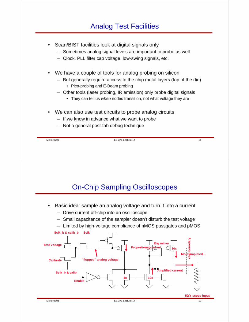
On-Chip Sampling Oscilloscopes
• Basic idea: sample an analog voltage and turn it into a current– Drive current off-chip into an oscilloscope
– Small capacitance of the sampler doesn’t disturb the test voltage
– Limited by high-voltage compliance of nMOS passgates and pMOS
50Ω 'scope input
chip
bo
un
dar
y
Big mirror
1x 10x
1x 10x
SclkSclk_b
Enable
Test Voltage
Calibrate
& calib_b
Sclk_b & calib
"flopped" analog voltage
Proportional current
Amplified current
More amplified…

EE 371 Lecture 14M Horowitz 13
Using Sampling Oscilloscopes
• Put the chip in a repeating mode, so the test waveform repeats
• Can run the sampler in “accurate mode”– Sampler clock has same frequency as chip clock (no LPF)
– Gradually walk the phase offsets between sampler and chip clocks
• Or, can run the sampler in “pretty mode”– Run sampler clock at slightly different frequency as chip clock
– “Walk” through the waveforms, and plot the curve on the scope
– Less accurate due to LPF at the input (charge-sharing)
• In both modes, jitter of sampler clock limits the BW of system
EE 371 Lecture 14M Horowitz 14
Sampling Oscilloscope Results
• Calibration is important – each sampler on the chip is different
• Sampled bitlines on a low-power memory compared to sims
Source: Ho, VLSI Symp ‘98
EE 371 Lecture 14M Horowitz 15
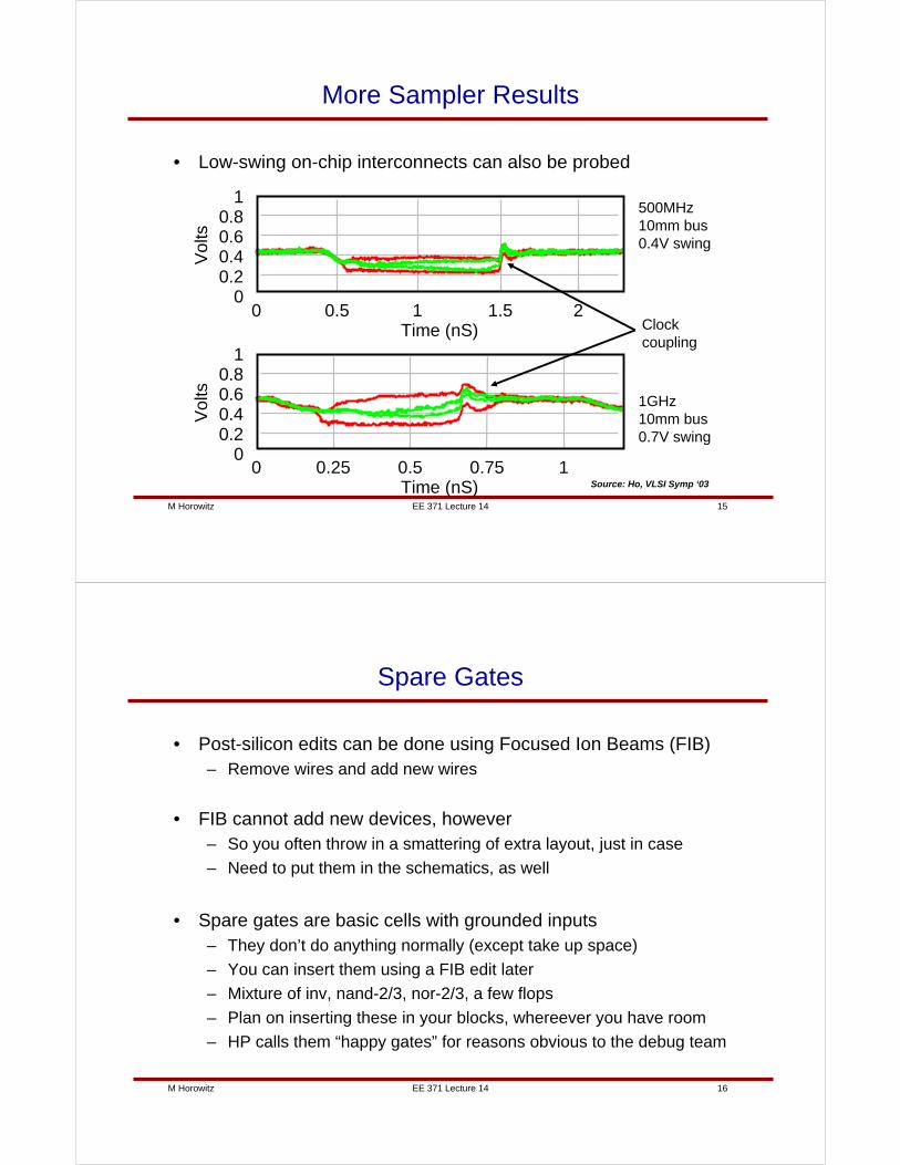
More Sampler Results
• Low-swing on-chip interconnects can also be probed
00.20.40.60.8
1
0 0.5 1 1.5 2
Vol
ts
Time (nS)
00.20.40.60.8
1
0 0.25 0.5 0.75 1
Vol
ts
Time (nS)
500MHz10mm bus0.4V swing
1GHz10mm bus0.7V swing
Clockcoupling
Source: Ho, VLSI Symp ‘03
EE 371 Lecture 14M Horowitz 16
Spare Gates
• Post-silicon edits can be done using Focused Ion Beams (FIB)– Remove wires and add new wires
• FIB cannot add new devices, however– So you often throw in a smattering of extra layout, just in case
– Need to put them in the schematics, as well
• Spare gates are basic cells with grounded inputs– They don’t do anything normally (except take up space)
– You can insert them using a FIB edit later
– Mixture of inv, nand-2/3, nor-2/3, a few flops
– Plan on inserting these in your blocks, whereever you have room
– HP calls them “happy gates” for reasons obvious to the debug team
EE 371 Lecture 14M Horowitz 17
Debugging a Chip
• Run parts on tester and exercise the clock shrink mechanisms– ODCS was discussed in the clocking section
– Can move an arbitrary clock early or late to test speedpath theories
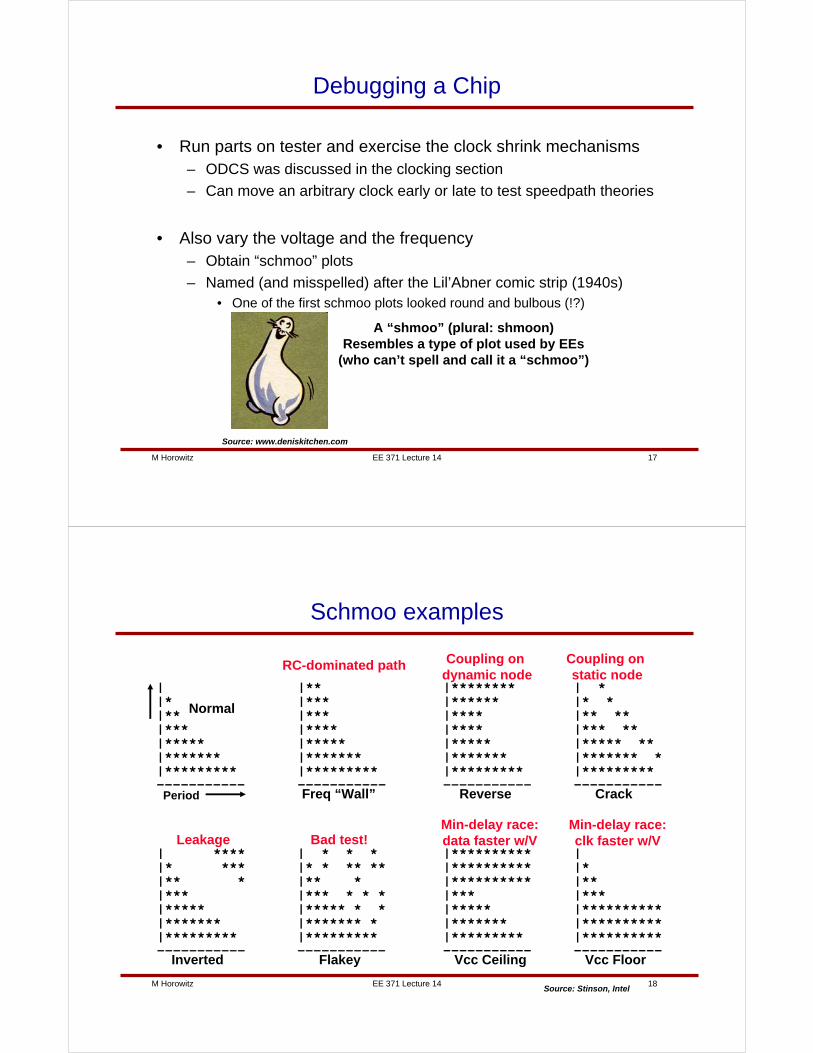
• Also vary the voltage and the frequency– Obtain “schmoo” plots
– Named (and misspelled) after the Lil’Abner comic strip (1940s)• One of the first schmoo plots looked round and bulbous (!?)
A “shmoo” (plural: shmoon)Resembles a type of plot used by EEs
(who can’t spell and call it a “schmoo”)
Source: www.deniskitchen.com
EE 371 Lecture 14M Horowitz 18
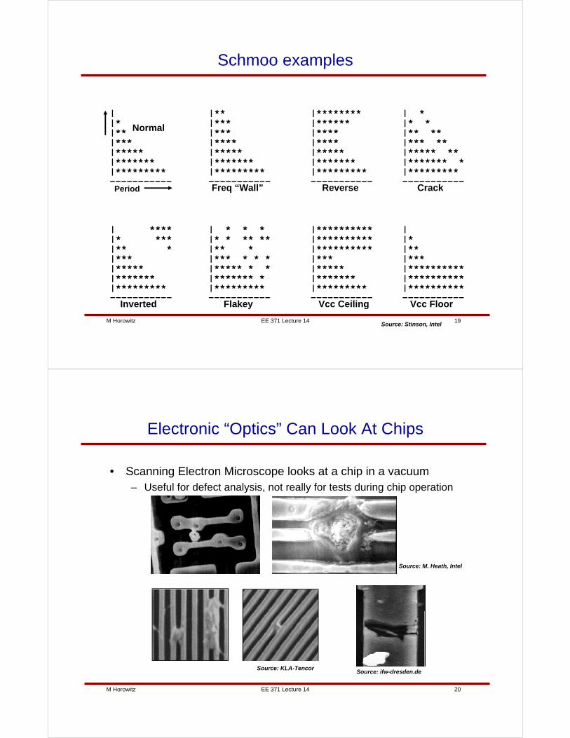
Schmoo examples
| |* |** |*** |***** |******* |*********-----------
Period
|** |*** |*** |**** |***** |******* |*********-----------
|**********|**********|**********|*** |***** |******* |*********-----------
| |* |** |*** |**********|**********|**********-----------
| * |* * |** ** |*** ** |***** ** |******* *|*********-----------
| ****|* ***|** *|*** |***** |******* |*********-----------
|******** |****** |**** |**** |***** |******* |*********-----------
| * * * |* * ** **|** * |*** * * *|***** * *|******* * |*********-----------
Freq “Wall” Reverse Crack
Inverted Flakey Vcc Ceiling Vcc Floor
Normal
RC-dominated path
Min-delay race:data faster w/V
Min-delay race:clk faster w/V
Coupling on dynamic node
Coupling on static node
Leakage Bad test!
Source: Stinson, Intel
EE 371 Lecture 14M Horowitz 19
Schmoo examples
| |* |** |*** |***** |******* |*********-----------
Period
|** |*** |*** |**** |***** |******* |*********-----------
|**********|**********|**********|*** |***** |******* |*********-----------
| |* |** |*** |**********|**********|**********-----------
| * |* * |** ** |*** ** |***** ** |******* *|*********-----------
| ****|* ***|** *|*** |***** |******* |*********-----------
|******** |****** |**** |**** |***** |******* |*********-----------
| * * * |* * ** **|** * |*** * * *|***** * *|******* * |*********-----------
Freq “Wall” Reverse Crack
Inverted Flakey Vcc Ceiling Vcc Floor
Normal
Source: Stinson, Intel
EE 371 Lecture 14M Horowitz 20
Electronic “Optics” Can Look At Chips
• Scanning Electron Microscope looks at a chip in a vacuum– Useful for defect analysis, not really for tests during chip operation
Source: M. Heath, Intel
Source: KLA-TencorSource: ifw-dresden.de

EE 371 Lecture 14M Horowitz 21
E-beam Probing and Controlling
• E-beam probing is a technique that requires face access– Shoot electrons at the chip and measure reflected electrons
– Grounded metals look bright; high-voltage metals look dark
– Can probe metals this way to find out their voltages
– Can also pulse e-beams at higher energy to charge up nodes• Mild form of controllability to go along with observability
Source: www.necel.com
EE 371 Lecture 14M Horowitz 22
Backside Access More Important Today
• Most chips are face-down and flip-chip bonded to package
• Covered already in the clock skew lecture, but briefly mention– PICA (IBM) and TRE (Intel)
• Capture photons (10-6/s rate) emitted from transistors that are switching
• Integrate over many many loops of the chip to build up a “movie”
– LVP (Intel): Laser voltage probing• Just like e-beam, but through a thinned back and aimed at diffusions
• Can see transitions, not voltage levels
• Should put a “probe diode” near a gate you believe will be critical
• In both techniques, it’s important to have alignment fiducials– The back of a die is otherwise flat, featureless, and boring

EE 371 Lecture 14M Horowitz 23
Laser Voltage Probe (LVP)
• Basic idea– Have picosecond pulse laser aimed at silicon
– Measure the reflectance (complex)
– Reflectance depends on carrier density• Which depends on depletion width, which depends on voltage
• Energy (light) absorbed by carriers in conduction band– Laser pointed at “backside” of transistors
• Requires “flip-chip” packaging
• Laser photon energy close to silicon band edge
• Wavelength kept in IR or NIR band (transparent thru silicon)
– Laser can induce carriers in conduction band• Need to keep intensity low enough to prevent inducing current
– Laser must be mode-locked to test• Must be sync’d to test loop length
EE 371 Lecture 14M Horowitz 24
Time Resolved Emission (TRE)
• Detects photons emitted by switching xtors (also called PICA)– Carriers in the channel “thermalize”, emitting NIR light
• Silicon is transparent to IR
– Need a REALLY good detector• Single photon per 10K switching events
• Photons go in all directions; detector only at one angle
• Need great timing resolution
– Completely non-invasive
– Collection times are significant• Longer time = better signal-to-noise ratio (SNR)
Pn+
Vgs > Vgs-Vt
-Pinch-off region

EE 371 Lecture 14M Horowitz 25
Light Emission from CMOS Circuits: Transient
A
B C
From P. Sanda
EE 371 Lecture 14M Horowitz 26
PICA Movie

EE 371 Lecture 14M Horowitz 27
LADA: Laser-Assisted Device Alteration
• Lasers can not only probe the voltages of diffusions– They can also control the behavior of the circuits
• Aim a 1.3μm wavelength laser at a circuit: heats up the circuits– Slows everything down
• Aim a 1.06μm wavelength laser at a circuit: generates e-/h+ pairs– nMOS devices have more current (in parallel with the device)
– pMOS devices have lower Vt (reduce rise delay, increase fall delay)
EE 371 Lecture 14M Horowitz 28
Using LADA
• Generate a theory why your chip fails – that circuit X is bad
• Run the ATE in a repeated mode and set environment “right”– Establish temperature, voltage, frequency so test *just* fails
– Now scan the laser, raster-style, over the block containing X
– See if the test passes; if so, note where laser was aimed
– Aha! The device at that location was critical
• Beware multiple unintended side effects– Leakage, conflicting speedpaths, etc.
EE 371 Lecture 14M Horowitz 29
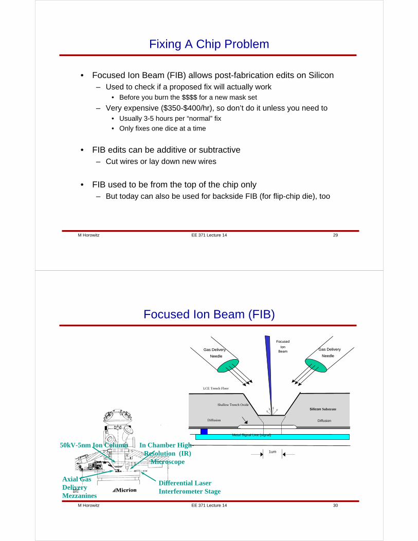
Fixing A Chip Problem
• Focused Ion Beam (FIB) allows post-fabrication edits on Silicon– Used to check if a proposed fix will actually work
• Before you burn the $$$$ for a new mask set
– Very expensive ($350-$400/hr), so don’t do it unless you need to• Usually 3-5 hours per “normal” fix
• Only fixes one dice at a time
• FIB edits can be additive or subtractive– Cut wires or lay down new wires
• FIB used to be from the top of the chip only– But today can also be used for backside FIB (for flip-chip die), too
EE 371 Lecture 14M Horowitz 30
Focused Ion Beam (FIB)
In Chamber High-Resolution (IR)
Microscope
Axial GasDeliveryMezzanines
Differential LaserInterferometer Stage
50kV-5nm Ion Column
Gas DeliveryGas Delivery
NeedleNeedle
Diffusion Diffusion
Shallow Trench Oxide
Metal Signal Line (signal)
Silicon Substrate
Gas DeliveryGas Delivery
NeedleNeedle
FocusedFocused
IonIonBeamBeam
LCE Trench Floor
1um

EE 371 Lecture 14M Horowitz 31
FIB example
A
B
C
FIB MetalDeposition
Old Signal
New Signal
FIB MetalDeposition
FIB Dielectric Deposition
FIB SignalCut
Location C
FIB ConnectionLocations A
& B
Diffusion
(new signal)
Silicon Substrate
Diffusion
(old signal)
Metal Line
FIB Cut Location
C
FIB Connection Location A
FIB Connection Location B
Source: Stinson, Intel
EE 371 Lecture 14M Horowitz 32
FIB for Probe
• The ability to do backside FIB enables mechanical probe– FIB a metal probe pad on the back of the silicon; tie to a diffusion
– Now you can break out those picoprobes that you had stored away
• Not great for high-bandwidth signals– Lots of extra cap, potentially inductance problems as well
– Better for Vdd and Gnd

EE 371 Lecture 14M Horowitz 33
Summary
• Debug is a huge and expensive effort
• Plan for debug in your design– Use scan, BIST, ATPG
– Build analog samplers if you know you’ll need to probe some node
– Insert spare gates in your blocks; you’ll probably need them
• Debug itself uses tester results and probing– Schmoos and clock shrinking can get you pretty far
– Test theories with mechanical or e-beam probing and lasers
• When you find the problem, call your FIB operator– FIB first before respinning the chip, to ensure the fix “takes”
EE 371 Lecture 14M Horowitz 34
Reliability
• Failure rates of devices follow a bathtub curve– Infant mortality: gross defects, poor manufacturing tolerances
– Useful life: problems arising from wear and tear, random errors
– Wear out: slower slope than infant side, but accelerated failures
Time
Fai
lure
rat
e, λ
λ Constant
Useful life Wear outInfantMortality
Source: klabs.org
EE 371 Lecture 14M Horowitz 35
Burn-In Ovens
• Can we accelerate the infant mortality portion of the curve?– Push all the parts into the “useful life” region
– Discard the ones that die and sell the rest with high confidence
• Use burn-in ovens to heat and simultaneously exercise the parts– Bump up temperature and voltage to get “acceleration factors”
– Temp held to 150o-200o and voltage to 1.5x-2x nominal (typically)
• Temperature depends on burn-in oven package solution– Package has a thermal resistivity, say ¼ oC/W (for example)
– Holding oven at 125oC for 100W parts means 150oC junction temp
EE 371 Lecture 14M Horowitz 36
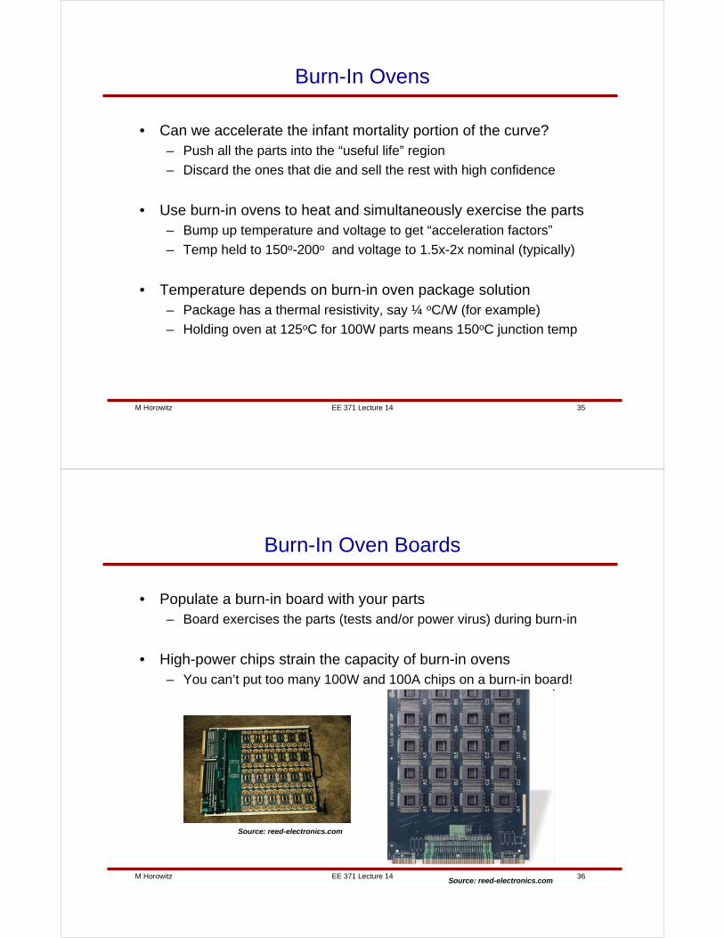
Burn-In Oven Boards
• Populate a burn-in board with your parts– Board exercises the parts (tests and/or power virus) during burn-in
• High-power chips strain the capacity of burn-in ovens– You can’t put too many 100W and 100A chips on a burn-in board!
Source: reed-electronics.com
Source: reed-electronics.com

EE 371 Lecture 14M Horowitz 37
Burn-In and Design
• Chips in the burn-in oven should work at those temps & voltages– Don’t want the artificial environment of burn-in to cause failures
• For example, higher leakage in burn-in shouldn’t cause failures– Domino gate with big nMOS
– Use a secondary keeper• Only in burn-in
• Combats elevated leakage
• Also an issue for > Vdd nodes– Burn in increases Vdd
Source: Chen, Broadcom
EE 371 Lecture 14M Horowitz 38
Reliability and Design
• Two examples of how designers worry about reliability
• Wires have reliability issues relating to wear-out– Electromigration for unidirectional current (depends on Iavg)
– Self-heating for bidirectional current (depends on Irms)
– Copper wires better than Aluminum, but still have limits
– Use minimum width rules based on total capacitance for layout
• Gates have reliability rules relating to hot-carrier degradation– Electrons in the channel can smack into the gate and “stick”
– Shift in Vt over time from charge trapping and general muckiness
– Regulate this by ensuring circuits are not “on” all the time
– Limit risetime of signals to be 20% of the cycle time (for example)

EE 371 Lecture 14M Horowitz 39
• The basic semantic for reliability is the FIT, or failure rate– “Failure in time” = failures per billion hours (note: 8760 hrs/yr)
• Time-to-failure uses Arrhenius’s model (1903 Nobel laureate)– Time-to-failure = (FIT)-1 = Const eEa/(kT) (k=8.6x10⁻⁵ eV/oK)
– Empirically estimate the activation energy Ea
– Gives the ratio of failure rates at different temps (Const drops out)
• Ex: test 900 parts for 1000 hours, and find 8 rejects at 100oC– If Ea was 1eV, what will be the failure rate at 30oC?
– 8 rejects/(900*1000) = 8.9x10⁻⁶ failure rate
– Ratio of TTFs from 100oC to 30oC = 1300, so FIT scales by 1/1300
– Failure rate at 30oC is about 6.84x10⁻⁹, or 6.84 FIT
Long-Term Reliability
EE 371 Lecture 14M Horowitz 40
• How cheesy is this, using Arrhenius’s equation? – Why do IC failures obey a chemical reaction rate model?
• Quite surprisingly, not that cheesy– Many failures initiated by atomic or molecular changes, e.g.:
Oxide/dielectric breakdown Ea = 0.8 eV
Electromigration Ea = 0.5 – 0.7 eV
Hot-carrier Vt degradation Ea = -0.2 eV (negative!)
– Physical failure modes are diverse, but obey temp relationship
• Some failures do NOT obey this model well– Solder ball stress fatigue, bad manufacturing tolerances, etc.
– Much more complex models out there
Long-Term Reliability
EE 371 Lecture 14M Horowitz 41
Other Reliability Issues
• Soft-errors and their prevention/mitigation affects design– Cosmic rays or α-particles smack into your silicon, inject electrons
– We will examine this in more depth next week
• Usually set design and layout rules based on a 10-year lifespan– Not well publicized; typical consumer believes ICs work forever
– Military specifications may well be different
Related Documents