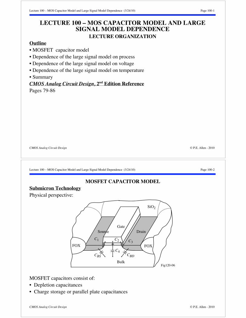
Lecture 100 – MOS Capacitor Model and Large Signal Model Dependence (3/24/10) Page 100-1 CMOS Analog Circuit Design © P.E. Allen - 2010 LECTURE 100 – MOS CAPACITOR MODEL AND LARGE SIGNAL MODEL DEPENDENCE LECTURE ORGANIZATION Outline • MOSFET capacitor model • Dependence of the large signal model on process • Dependence of the large signal model on voltage • Dependence of the large signal model on temperature • Summary CMOS Analog Circuit Design, 2 nd Edition Reference Pages 79-86 Lecture 100 – MOS Capacitor Model and Large Signal Model Dependence (3/24/10) Page 100-2 CMOS Analog Circuit Design © P.E. Allen - 2010 MOSFET CAPACITOR MODEL Submicron Technology Physical perspective: SiO 2 Bulk Source Drain Gate C BS C BD C 4 C 1 C 2 C 3 Fig120-06 FOX FOX MOSFET capacitors consist of: • Depletion capacitances • Charge storage or parallel plate capacitances

Welcome message from author
This document is posted to help you gain knowledge. Please leave a comment to let me know what you think about it! Share it to your friends and learn new things together.
Transcript
Lecture 100 – MOS Capacitor Model and Large Signal Model Dependence (3/24/10) Page 100-1
CMOS Analog Circuit Design © P.E. Allen - 2010
LECTURE 100 – MOS CAPACITOR MODEL AND LARGESIGNAL MODEL DEPENDENCE
LECTURE ORGANIZATIONOutline• MOSFET capacitor model• Dependence of the large signal model on process• Dependence of the large signal model on voltage• Dependence of the large signal model on temperature• SummaryCMOS Analog Circuit Design, 2nd Edition ReferencePages 79-86
Lecture 100 – MOS Capacitor Model and Large Signal Model Dependence (3/24/10) Page 100-2
CMOS Analog Circuit Design © P.E. Allen - 2010
MOSFET CAPACITOR MODELSubmicron TechnologyPhysical perspective:
SiO2
Bulk
Source DrainGate
CBS CBD
C4
C1 C2 C3
Fig120-06
FOX FOX
MOSFET capacitors consist of:• Depletion capacitances• Charge storage or parallel plate capacitances

Lecture 100 – MOS Capacitor Model and Large Signal Model Dependence (3/24/10) Page 100-3
CMOS Analog Circuit Design © P.E. Allen - 2010
Deep Submicron TechnologyPhysical perspective:
MOSFET capacitors consist of:• Depletion capacitances• Charge storage or parallel plate capacitances
Lecture 100 – MOS Capacitor Model and Large Signal Model Dependence (3/24/10) Page 100-4
CMOS Analog Circuit Design © P.E. Allen - 2010
MOSFET Depletion CapacitorsModel:1.) vBS FC·PB
CBS = CJ·AS
1 -vBSPB
MJ + CJSW·PS
1 -vBSPB
MJSW,
and2.) vBS> FC·PB
CBS = CJ·AS
1- FC1+MJ 1 - (1+MJ)FC + MJ
VBSPB
+ CJSW·PS
1 - FC1+MJSW 1 - (1+MJSW)FC + MJSW
VBSPB
SiO2
Polysilicon gate
Bulk
A B
CD
EF
GH
Drain bottom = ABCDDrain sidewall = ABFE + BCGF + DCGH + ADHE
Source Drain
Fig. 120-07
FC·PB
PB
vBS
CBS
vBS ≤ FC·PBvBS ≥ FC·PB
Fig. 120-08
whereAS = area of the sourcePS = perimeter of the sourceCJSW = zero bias, bulk source sidewall capacitanceMJSW = bulk-source sidewall grading coefficient
For the bulk-drain depletion capacitance replace "S" by "D" in the above.

Lecture 100 – MOS Capacitor Model and Large Signal Model Dependence (3/24/10) Page 100-5
CMOS Analog Circuit Design © P.E. Allen - 2010
SM Charge Storage (Parallel Plate) MOSFET Capacitances - C1, C2, C3 and C4
Overlap capacitances:C1 = C3 = LD·Weff·Cox = CGSO or CGDO(LD 0.015 μm for LDD structures)
Channel capacitances:C2 = gate-to-channel = CoxW eff·(L-2LD) =
CoxW eff·LeffC4 = voltage dependent channel-
bulk/substrate capacitanceBulk
LDMask
W
Oxide encroachment
ActualL (Leff)
Gate
Mask L
Source-gate overlapcapacitance CGS (C1)
Drain-gate overlapcapacitance CGD (C3)
ActualW (Weff)
Fig. 120-09
Source
Gate
Drain
Gate-ChannelCapacitance (C2)
Channel-BulkCapacitance (C4)
FOX FOX
Lecture 100 – MOS Capacitor Model and Large Signal Model Dependence (3/24/10) Page 100-6
CMOS Analog Circuit Design © P.E. Allen - 2010
SM Charge Storage (Parallel Plate) MOSFET Capacitances - C5View looking down the channel from source to drain
Bulk
Overlap Overlap
Source/DrainGate
FOX FOXC5 C5
Fig120-10
C5 = CGBOCapacitance values based on an oxide thickness of 140 Å or Cox=24.7 10-4 F/m2:
Type P-Channel N-Channel UnitsCGSO 220 10-12 220 10-12 F/mCGDO 220 10-12 220 10-12 F/mCGBO 700 10-12 700 10-12 F/mCJ 560 10-6 770 10-6 F/m2
CJSW 350 10-12 380 10-12 F/mMJ 0.5 0.5MJSW 0.35 0.38
Lecture 100 – MOS Capacitor Model and Large Signal Model Dependence (3/24/10) Page 100-7
CMOS Analog Circuit Design © P.E. Allen - 2010
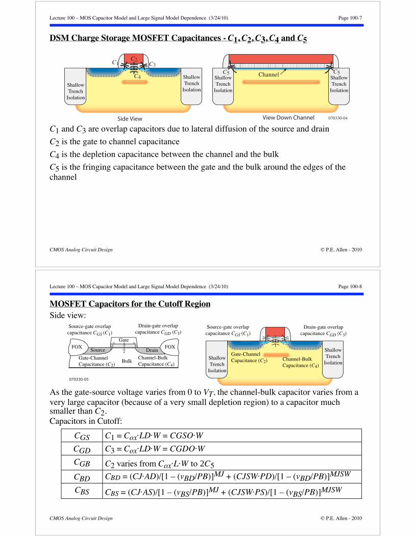
DSM Charge Storage MOSFET Capacitances - C1, C2, C3, C4 and C5
ShallowTrench
IsolationShallowTrench
Isolation
ShallowTrench
Isolation
ShallowTrench
Isolation
C1
C5C5
C2
C4
C3
Side View View Down Channel 070330-04
Channel
C1 and C3 are overlap capacitors due to lateral diffusion of the source and drain
C2 is the gate to channel capacitance
C4 is the depletion capacitance between the channel and the bulk
C5 is the fringing capacitance between the gate and the bulk around the edges of thechannel
Lecture 100 – MOS Capacitor Model and Large Signal Model Dependence (3/24/10) Page 100-8
CMOS Analog Circuit Design © P.E. Allen - 2010
MOSFET Capacitors for the Cutoff RegionSide view:
Bulk
Source-gate overlapcapacitance CGS (C1)
Drain-gate overlapcapacitance CGD (C3)
Source
Gate
Drain
Gate-ChannelCapacitance (C2)
Channel-BulkCapacitance (C4)
FOX FOX
ShallowTrench
Isolation
ShallowTrench
Isolation
Source-gate overlapcapacitance CGS (C1)
Drain-gate overlapcapacitance CGD (C3)
Gate-ChannelCapacitance (C2) Channel-Bulk
Capacitance (C4)
070330-05
As the gate-source voltage varies from 0 to VT, the channel-bulk capacitor varies from avery large capacitor (because of a very small depletion region) to a capacitor muchsmaller than C2.Capacitors in Cutoff:
CGS C1 = Cox·LD·W = CGSO·W
CGD C3 = Cox·LD·W = CGDO·W
CGB C2 varies from Cox·L·W to 2C5
CBD CBD = (CJ·AD)/[1 – (vBD/PB)]MJ + (CJSW·PD)/[1 – (vBD/PB)]MJSW
CBS CBS = (CJ·AS)/[1 – (vBS/PB)]MJ + (CJSW·PS)/[1 – (vBS/PB)]MJSW

Lecture 100 – MOS Capacitor Model and Large Signal Model Dependence (3/24/10) Page 100-9
CMOS Analog Circuit Design © P.E. Allen - 2010
MOSFET Capacitors for the Saturation RegionSide view:
Bulk
Source-gate overlapcapacitance CGS (C1)
Drain-gate overlapcapacitance CGD (C3)
Source
Gate
DrainGate-ChannelCapacitance (C2)
FOX FOXShallowTrench
Isolation
ShallowTrench
Isolation
070330-06
Source-gate overlapcapacitance CGS (C1)
Drain-gate overlapcapacitance CGD (C3)
Gate-ChannelCapacitance (C2)
In the saturation region, C4, becomes small and is not shown above.
Capacitors in Saturation:
CGS C1 = Cox·LD·W + (2/3)Cox·L·W = [CGSO + (2/3)Cox·L]W
CGD C3 = Cox·LD·W = CGDO·W
CGB 2C5 = 2·CGBO·W
CBD CBD = (CJ·AD)/[1 – (vBD/PB)]MJ + (CJSW·PD)/[1 – (vBD/PB)]MJSW
CBS CBS = (CJ·AS)/[1 – (vBS/PB)]MJ + (CJSW·PS)/[1 – (vBS/PB)]MJSW
Lecture 100 – MOS Capacitor Model and Large Signal Model Dependence (3/24/10) Page 100-10
CMOS Analog Circuit Design © P.E. Allen - 2010
MOSFET Capacitors for the Active RegionSide view:
Bulk
Source-gate overlapcapacitance CGS (C1)
Drain-gate overlapcapacitance CGD (C3)
Source
Gate
Drain
Gate-ChannelCapacitance (C2)
FOX FOXShallowTrench
Isolation
ShallowTrench
Isolation
070330-07
Source-gate overlapcapacitance CGS (C1)
Drain-gate overlapcapacitance CGD (C3)
Gate-ChannelCapacitance (C2)
In the saturation region, C4, becomes small and is not shown above.
Capacitors in Active:
CGS C1 = Cox·LD·W + (1/2)Cox·L·W = [CGSO + (1/2)Cox·L]W
CGD C3 = Cox·LD·W + (1/2)Cox·L·W = [CGSO + (1/2)Cox·L]W
CGB 2C5 = 2·CGBO·W
CBD CBD = (CJ·AD)/[1 – (vBD/PB)]MJ + (CJSW·PD)/[1 – (vBD/PB)]MJSW
CBS CBS = (CJ·AS)/[1 – (vBS/PB)]MJ + (CJSW·PS)/[1 – (vBS/PB)]MJSW

Lecture 100 – MOS Capacitor Model and Large Signal Model Dependence (3/24/10) Page 100-11
CMOS Analog Circuit Design © P.E. Allen - 2010
Illustration of CGD, CGS and CGBComments on the variation of CBG in the cutoff region:
CBG = 1
1C2 +
1C4
+ 2C5
1.) For vGS 0, CGB C2 + 2C5
(C4 is large because of the thin
inversion layer in weak inversion
where VGS is slightly less than VT))
2.) For 0 < vGS VT, CGB 2C5(C4 is small because of the thickerinversion layer in strong inversion)
0 vGS
CGS
CGS, CGD
CGDCGB
CGS, CGD
C2 + 2C5
C1+ 0.67C2
C1, C32C5
VT vDS +VT
Off Saturation Non-Saturation
vDS = constant vBS = 0
Capacitance
C1+ 0.5C2
Fig120-12
C4 Large
C4 Small
Lecture 100 – MOS Capacitor Model and Large Signal Model Dependence (3/24/10) Page 100-12
CMOS Analog Circuit Design © P.E. Allen - 2010
DEPENDENCE OF THE LARGE SIGNAL MODEL ON PROCESSHow Does Technology Vary?1.) Thickness variations in layers (dielectrics and metal)
060225-01
tox(min) tox(max)
2.) Doping variations
3.) Process biases – differences betweenthe drawn and actual dimensions due to process (etching, lateral diffusion, etc.)
060225-03
Drawn Dimension
Actual Dimension
060225-02
n-well
p+n+ p+
Diffusion Differences

Lecture 100 – MOS Capacitor Model and Large Signal Model Dependence (3/24/10) Page 100-13
CMOS Analog Circuit Design © P.E. Allen - 2010
Large Signal Model Dependence on Process Variations1.) Threshold voltage
VT = VT0 + |-2 F + vSB| - |-2 F|
where
VT0 = MS - 2 F - Qb0
Cox -
QSS
Cox and =
2q siNA
Cox
If VBS = 0, then VT is dependent on doping and oxide thickness because
F = kTq ln
NSUBni
and Cox 1
tox
(Recall that the threshold is also determined by the threshold implant during processing)
2.) Transconductance parameter
K’ = μoCox 1
tox
For short channel devices, the mobility is degraded as given by
μeff = μo
1 + (VGS - VT) and 2x10⁻⁹m/V
tox
Lecture 100 – MOS Capacitor Model and Large Signal Model Dependence (3/24/10) Page 100-14
CMOS Analog Circuit Design © P.E. Allen - 2010
Process Variation “Corners”For strong inversion operation, the primary influence is the oxide thickness, tox. We seethat K’ will tend to increase with decreasing oxide thickness whereas VT tends todecrease.If the “speed” of a transistor is increasedby increasing K’ and decreasing VT, thenthe variation of technology can beexpressed on a two-dimensional graphresulting in a rectangular area of“acceptable” process limitation.
Three corner versus five corner models060118-10
PMOSSpeed
NMOS Speed
Fast PMOS
SlowPMOS
SlowNMOS
FastNMOS
AcceptableTechnologyParameters
Large KʼSmall VT
Small KʼLarge VT
Lecture 100 – MOS Capacitor Model and Large Signal Model Dependence (3/24/10) Page 100-15
CMOS Analog Circuit Design © P.E. Allen - 2010
DEPENDENCE OF THE LARGE SIGNAL MODEL ON VOLTAGEWhat is Voltage Variation?Voltage variation is the influence of power supply voltage on the component.(There is also power supply influence on the circuit called power supply rejection ratio,PSRR. We will deal with this much later.)Power supply variation comes from:1.) Influence of depletion region widths on components.2.) Nonlinearity3.) Breakdown voltage
Note: Because the large-signal model for the MOSFET includes all the influences ofvoltage on the transistor, we will focus on passive components except for breakdown.
Lecture 100 – MOS Capacitor Model and Large Signal Model Dependence (3/24/10) Page 100-16
CMOS Analog Circuit Design © P.E. Allen - 2010
Models for Voltage Dependence of a Component1.) ith-order Voltage Coefficients
In general a variable y = f(v) which is a function of voltage, v, can be expressed as aTaylor series,
y(v = V0) y(V0) + a1(v- V0) + a2(v- V0)2+ a3(v- V0)3 + ···where the coefficients, ai, are defined as,
a1 = df(v)dv
|v=V0 , a2 =
12
d2f(v)dv2
|v=V0 , ….
The coefficients, ai, are called the first-order, second-order, …. voltage coefficients.
2.) Fractional Voltage Coefficient or Voltage CoefficientGenerally, only the first-order coefficients are of interest.In the characterization of temperature dependence, it is common practice to use a termcalled fractional voltage coefficient, VCF, which is defined as,
VCF(v=V0) = 1
f(v=V0) df(v)dv
|v=V0 parts per million/V (ppm/V)
or more simply,
VCF = 1
f(v) df(v)dv parts per million/V (ppm/V)

Lecture 100 – MOS Capacitor Model and Large Signal Model Dependence (3/24/10) Page 100-17
CMOS Analog Circuit Design © P.E. Allen - 2010
Influence of Voltage on a Diffused Resistor – Depletion Region
Influence of the depletion region on the p+ resistor:
060305-01
p- substrate
p+
Older LOCOS Technology
p+
n-well
STI STI
p+
Depletion region
Thickness ofp+ Resistor
n- well
FOX FOX
Thickness ofp+ Resistor
As the voltage at the terminals of the resistor become smaller than the n-well potential,the depletion region will widen causing the thickness of the resistor to decrease.
R = L
t W VR
where VR is the reverse bias voltage from the resistor to the well.
This effect is worse for well resistors because the doping concentration of the resistor issmaller.Voltage coefficient for diffused resistors 200-800 ppm/VVoltage coefficient for well resistors 8000 ppm/V
Lecture 100 – MOS Capacitor Model and Large Signal Model Dependence (3/24/10) Page 100-18
CMOS Analog Circuit Design © P.E. Allen - 2010
Voltage Coefficient of Polysilicon ResistorsWhy should polysilicon resistors be sensitive to voltage?There is a small depletion region between the polysilicon and its surrounding materialthat has a very small dependence on the voltage between the polysilicon and thesurrounding material.

Lecture 100 – MOS Capacitor Model and Large Signal Model Dependence (3/24/10) Page 100-19
CMOS Analog Circuit Design © P.E. Allen - 2010
Voltage Nonlinearity and Breakdown VoltageConductivity modulation:As the current in a resistor increases, the conductivity becomes modulated and theresistance increases.Example of a n-well resistor:
As the reverse bias voltage across a pn junctionbecomes large, at some point, called the breakdownvoltage, the current will rapidly increase. Bothtransistors, diodes and depletion capacitors experiencethis breakdown.Model for current multiplication factor:
M = 1
1 +vRBV
n
060311-01
i
v
i = vR
Conductivitymodulation
0.1A
060311-02
iR
vR
Breakdownvoltage
BV
Lecture 100 – MOS Capacitor Model and Large Signal Model Dependence (3/24/10) Page 100-20
CMOS Analog Circuit Design © P.E. Allen - 2010
DEPENDENCE OF THE LARGE SIGNAL MODEL ON TEMPERATURETemperature Dependence of the MOSFETTransconductance parameter:
K’(T) = K’(T0) (T/T0)-1.5 (Exponent becomes +1.5 below 77°K)
Threshold Voltage:VT(T) = VT(T0) + (T-T0) + ···
Typically NMOS = -2mV/°C to –3mV/°C from 200°K to 400°K (PMOS has a + sign)
ExampleFind the value of ID for a NMOS transistor at 27°C and 100°C if VGS = 2V and W/L =
5μm/1μm if K’(T0) = 110μA/V2 and VT(T0) = 0.7V and T0 = 27°C and NMOS = -2mV/°C.
SolutionAt room temperature, the value of drain current is,
ID(27°C) = 110μA/V2·5μm
2·1μm (2-0.7)2 = 465μA
At T = 100°C (373°K), K’(100°C)=K’(27°C) (373/300)-1.5=110μA/V2·0.72=79.3μA/V2
and VT(100°C) = 0.7 – (.002)(73°C) = 0.554V
ID(100°C) = 79.3μA/V2·5μm
2·1μm (2-0.554)2 = 415μA (Repeat with VGS = 2.0855V)
Lecture 100 – MOS Capacitor Model and Large Signal Model Dependence (3/24/10) Page 100-21
CMOS Analog Circuit Design © P.E. Allen - 2010
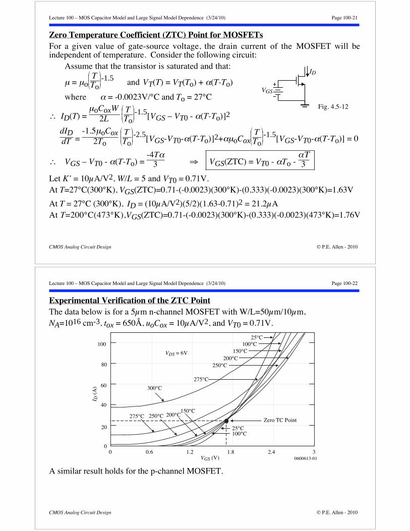
Zero Temperature Coefficient (ZTC) Point for MOSFETsFor a given value of gate-source voltage, the drain current of the MOSFET will beindependent of temperature. Consider the following circuit:
Assume that the transistor is saturated and that:
μ = μo
TTo
-1.5 and VT(T) = VT(To) + (T-To)
where = -0.0023V/°C and To = 27°C
ID(T) = μoCoxW
2L TTo
-1.5[VGS – VT0 - (T-To)]2
dIDdT =
-1.5μoCox
2To
TTo
-2.5[VGS-VT0- (T-To)]2+ μoCox
TTo
-1.5[VGS-VT0- (T-To)] = 0
VGS – VT0 - (T-To) = -4T
3 VGS(ZTC) = VT0 - To - 3
Let K’ = 10μA/V2, W/L = 5 and VT0 = 0.71V.At T=27°C(300°K), VGS(ZTC)=0.71-(-0.0023)(300°K)-(0.333)(-0.0023)(300°K)=1.63V
At T = 27°C (300°K), ID = (10μA/V2)(5/2)(1.63-0.71)2 = 21.2μAAt T=200°C(473°K),VGS(ZTC)=0.71-(-0.0023)(300°K)-(0.333)(-0.0023)(473°K)=1.76V
ID
VGS
Fig. 4.5-12
Lecture 100 – MOS Capacitor Model and Large Signal Model Dependence (3/24/10) Page 100-22
CMOS Analog Circuit Design © P.E. Allen - 2010
Experimental Verification of the ZTC PointThe data below is for a 5μm n-channel MOSFET with W/L=50μm/10μm,NA=1016 cm-3, tox = 650Å, uoCox = 10μA/V2, and VT0 = 0.71V.
0600613-01
0
20
40
60
80
100
0 0.6 1.2 1.8 2.4 3
25°C100°C
150°C200°C250°C275°C
300°C
VDS = 6V
Zero TC Point
25°C100°C
150°C200°C
250°C
275°C
VGS (V)
I D (
A)
A similar result holds for the p-channel MOSFET.

Lecture 100 – MOS Capacitor Model and Large Signal Model Dependence (3/24/10) Page 100-23
CMOS Analog Circuit Design © P.E. Allen - 2010
ZTC Point for UDSM Technology50 nm CMOS:
0 0.1 0.2 0.3 0.4 0.5 0.6 0.7 0.8 0.9 1.0
0
0.1
0.2
0.3
0.4
0.5
0.6
0.7
Nor
mal
ized
Dra
in C
urre
nt
Gate Source Voltage
25°C
50°C
100°C
140°CNMOS
L=500nm
Zero TemperatureCoefficient
071108-02
0.8
0.9
1.0
Note that the ZTC point is close to VDD.
PMOS will have similar characteristics.
0 0.1 0.2 0.3 0.4 0.5 0.6 0.7 0.8 0.9 1.00
0.1
0.2
0.3
0.4
0.5
0.6
0.7
Nor
mal
ized
Dra
in C
urre
nt
Gate Source Voltage
25°C50°C100°C140°C
NMOSL=50nm
Zero TemperatureCoefficient
071108-01
Lecture 100 – MOS Capacitor Model and Large Signal Model Dependence (3/24/10) Page 100-24
CMOS Analog Circuit Design © P.E. Allen - 2010
Bulk-Drain (Bulk-Source) Leakage Currents
Cross-section of a NMOS in a p-well:VGS>VT:
VGS<VT:
���Polysilicon
p+
n- substrate
Fig.3.6-5
VG > VT VD > VDS(sat)
��������������n+n+
DepletionRegion
B S
p-well
����
���������Polysilicon
p+
n- substrate
Fig.3.6-6
VG <VT VD > VDS(sat)
n+n+
DepletionRegion
B S
p-well

Lecture 100 – MOS Capacitor Model and Large Signal Model Dependence (3/24/10) Page 100-25
CMOS Analog Circuit Design © P.E. Allen - 2010
Temperature Modeling of the PN JunctionPN Junctions (Reverse-biased only):
iD Is = qA Dppno
Lp+
DnnpoLn
qAD
L n
2i
N = KT 3exp VGo
Vt
Differentiating with respect to temperature gives,dIs
dT = 3KT 3
T exp VGo
Vt +
qKT 3VGo
KT 2 exp VGo
Vt =
3Is
T + Is
T VGo
Vt
TCF = dIs
IsdT = 3T +
1T
VGoVt
ExampleAssume that the temperature is 300° (room temperature) and calculate the reversediode current change and the TCF for a 5° increase.SolutionThe TCF can be calculated from the above expression as TCF = 0.01 + 0.155 = 0.165.Since the TCF is change per degree, the reverse current will increase by a factor of 1.165for every degree (or °C) change in temperature. Multiplying by 1.165 five times givesan increase of approximately 2. Thus, the reverse saturation current approximatelydoubles for every 5°C temperature increase.Experimentally, the reverse current doubles for every 8°C increase in temperaturebecause the reverse current is in part leakage current.
Lecture 100 – MOS Capacitor Model and Large Signal Model Dependence (3/24/10) Page 100-26
CMOS Analog Circuit Design © P.E. Allen - 2010
Experimental Verification of the PN Junction Temperature Dependence
Theory:
Is(T) T 3 expVG(T)
kT

Lecture 100 – MOS Capacitor Model and Large Signal Model Dependence (3/24/10) Page 100-27
CMOS Analog Circuit Design © P.E. Allen - 2010
Temperature Modeling of the PN Junction – ContinuedPN Junctions (Forward biased – vD constant):
iD Is exp vDVt
Differentiating this expression with respect to temperature and assuming that the diodevoltage is a constant (vD = VD) gives
diDdT =
iDIs
dIsdT -
1T
VDVt
iD
The fractional temperature coefficient for iD is1iD
diDdT =
1Is
dIsdT -
VDTVt
= 3T +
VGo - VDTVt
If VD is assumed to be 0.6 volts, then the fractional temperature coefficient is equal to0.01+(0.155-0.077) = 0.0879. The forward diode current will approx. double for a 10°C.PN Junctions (Forward biased – iD constant):
VD = Vt ln(ID/Is)Differentiating with respect to temperature gives
dvDdT =
vDT - Vt
1Is
dIsdT =
vDT -
3VtT -
VGoT = -
VGo - vDT -
3VtT
Assuming that vD = VD = 0.6 V the temperature dependence of the forward diode voltageat room temperature is approximately -2.3 mV/°C.
Lecture 100 – MOS Capacitor Model and Large Signal Model Dependence (3/24/10) Page 100-28
CMOS Analog Circuit Design © P.E. Allen - 2010
Resistor Dependence on TemperatureDiffused Resistors:The temperature dependence of resistors depends mostly on the doping level of diffusedand implanted resistors. As the doping level or sheet resistance increases from 100 /to 400 / , the temperature coefficient varies from about +1000 ppm/°C to +4000ppm/°C. Diffused and implanted resistors have good thermal conduction to the substrateor well.Polysilicon Resistors:
Typically has a sheet resistance of 20 / to 80 / and has poor thermal conductionbecause it is electrically isolated by oxide layers.Metal:Metal is often used for resistors and has a positive temperature coefficient.Temperature Coefficients of Resistors:
n-well = 4000 ppm/°C Diffusion = +1500 ppm/°CPolysilicon = 500-2000 ppm/°C Ion implanted = +400 ppm/°CMetal = +3800 ppm/°C (aluminum)

Lecture 100 – MOS Capacitor Model and Large Signal Model Dependence (3/24/10) Page 100-29
CMOS Analog Circuit Design © P.E. Allen - 2010
SUMMARY• The large signal capacitance model includes depletion and parallel plate capacitors• The depletion capacitors CBD and CBS vary with their reverse bias voltage
• The capacitors CGD, CGS, and CGB have different values for the regions of cutoff, activeand saturated
• The large signal model varies with process primarily through μo and tox
• Voltage dependence of resistors and capacitors is primarily due to the influence ofdepletion regions
• The temperature dependent large signal model of the MOSFET yields a gate-sourcevoltage where the derivative of drain current with respect to temperature is zero
• Other MOSFET temperature dependence comes from the leakage currents acrossreverse biased pn junctions
Related Documents