Lecture 09 NAND and XOR Implementations

Welcome message from author
This document is posted to help you gain knowledge. Please leave a comment to let me know what you think about it! Share it to your friends and learn new things together.
Transcript

Lecture 09
NAND and XOR Implementations
Overview
° Developing NAND circuits
° Two-level implementations• Convert from AND/OR to NAND (again!)
° Multi-level NAND implementations• Convert from a network of AND/ORs
° Exclusive OR • Comparison with SOP
° Parity checking and detecting circuitry• Efficient with XOR gates!

Gates
A X X = (A + B)’B
AND A X = A • B X orB X = AB
0 0 0 0 1 0 1 0 0 1 1 1
0 0 0 0 1 1 1 0 1 1 1 1
OR A X X = A + BB
I A X X = A’0 11 0
Buffer A X X = A A X0 01 1
NANDA X X = (AB)’B
0 0 10 1 11 0 11 1 0
NOR0 0 10 1 01 0 01 1 0
XORExclusive OR
A X = A B X orB X = A’B + AB’
0 0 00 1 11 0 11 1 0
A X = (A B)’ X orB X = A’B’+ AB
0 0 10 1 01 0 01 1 1
XNORExclusive NORor Equivalence
A B X
A B X
A X
A B X
A B X
A B X
A B X

Axioms and Graphical representation of DeMorgan's Law
Y X Y X 14B)
Y X YX 14A)
YXYXX 13D)
YXYXX 13C)
YXXYX 13B)
YXYXX 13A)
YZYWXZXWZWYX 12B)
XZXYZYX 12A)
ZYXZY X 11B)
ZXYYZX 11A)
X Y Y X 10B)
X Y Y X 10A)
Commutative
Law
Associative Law
Distributive Law
Consensus Theorem

nand
nor
and
or
not
• Recall that symbolic DeMorgan’s duals exist for all gate primitives
• The above alternate symbols can be used to facilitate the analysis and design of NAND and NOR gate networks.
Network Conversion Using Alternate Gate Symbols

NAND-NAND & NOR-NOR Networks
DeMorgan’s Law:
(a + b)’ = a’ b’ (a b)’ = a’ + b’
a + b = (a’ b’)’ (a b) = (a’ + b’)’
push bubbles or introduce in pairs or remove pairs.
= =
==

NAND-NAND & NOR-NOR Networks
= =
==

NAND-NAND Networks
° Mapping from AND/OR to NAND/NAND
ab
cd
a) b)
c) d)

NAND-NAND Networks

Implementations of Two-level Logic
° Sum-of-products• AND gates to form product terms
(minterms)
• OR gate to form sum
° Product-of-sums• OR gates to form sum terms
(maxterms)
• AND gates to form product

Two-level Logic using NAND Gates
° Replace minterm AND gates with NAND gates
° Place compensating inversion at inputs of OR gate

Two-level Logic using NAND Gates (cont’d)
° OR gate with inverted inputs is a NAND gate• de Morgan's: A' + B' = (A • B)'
° Two-level NAND-NAND network• Inverted inputs are not counted
• In a typical circuit, inversion is done once and signal distributed

Two-level Logic using NAND Gates (cont’d)
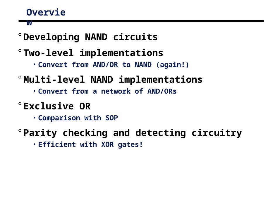
Conversion Between Forms
° Convert from networks of ANDs and ORs to networks of NANDs and NORs
• Introduce appropriate inversions ("bubbles")
° Each introduced "bubble" must be matched by a corresponding "bubble"
• Conservation of inversions
• Do not alter logic function
° Example: AND/OR to NAND/NAND
A
B
C
D
Z
A
B
C
D
Z
NAND
NAND
NAND

Z = [ (A • B)' • (C • D)' ]'
= [ (A' + B') • (C' + D') ]'
= [ (A' + B')' + (C' + D')' ]
= (A • B) + (C • D)
Conversion Between Forms (cont’d)
° Example: verify equivalence of two forms
A
B
C
D
Z
A
B
C
D
Z
NAND
NAND
NAND

Conversion to NAND Gates
° Start with SOP (Sum of Products)• circle 1s in K-maps
° Find network of OR and AND gates

ABC
DE
FG
X
Multi-level Logic
° x = A D F + A E F + B D F + B E F + C D F + C E F + G• Reduced sum-of-products form – already simplified
• 6 x 3-input AND gates + 1 x 7-input OR gate (may not exist!)
• 25 wires (19 literals plus 6 internal wires)
° x = (A + B + C) (D + E) F + G• Factored form – not written as two-level S-o-P
• 1 x 3-input OR gate, 2 x 2-input OR gates, 1 x 3-input AND gate
• 10 wires (7 literals plus 3 internal wires)

Level 1 Level 2 Level 3 Level 4
originalAND-OR network
A
CD
B
BC ’
F
introduction andconservation of
bubblesA
CD
B
BC ’
F
redrawn in termsof conventional
NAND gates A
CD
B ’
BC ’
F
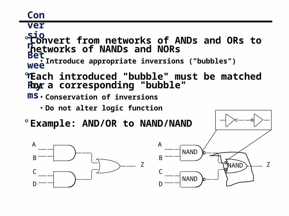
Conversion of Multi-level Logic to NAND Gates° F = A (B + C D) + B C'
A
XBCD
F(a)
Original circuit
A
XBC
D
F(b)
Add double bubbles at inputs
D ’
A
X ’
BC
F(c)
Distribute bubblessome mismatches
D ’
AX
BC
FX ’
(d)
Insert inverters to fix mismatches
Conversion Between Forms
° Example

Making NAND circuits (Ex)° The easiest way to make a NAND circuit is to start with
a regular, primitive gate-based diagram.
° Two-level circuits are trivial to convert, so here is a slightly more complex random example.

Converting to a NAND° Step 1: Convert all AND gates to NAND gates and
convert all OR gates to NAND gates.
AND
AND
AND
AND
OR
OR

Converting to NAND° Step 2: Cancel all pairs of inverters ((x’)’ = x)..
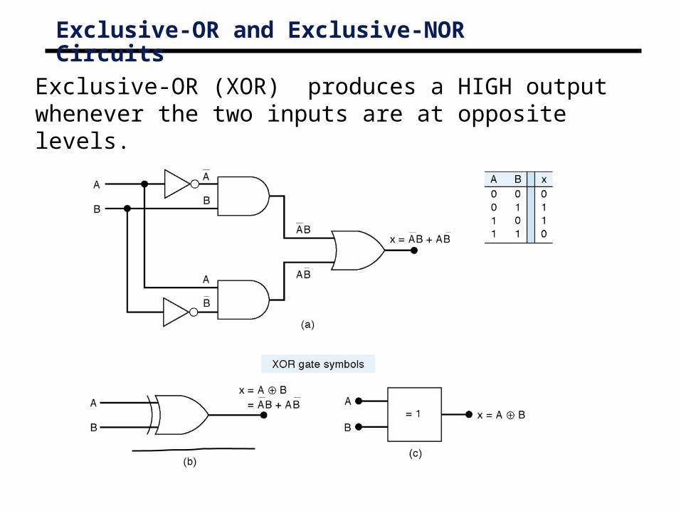
Exclusive-OR and Exclusive-NOR Circuits
Exclusive-OR (XOR) produces a HIGH output whenever the two inputs are at opposite levels.
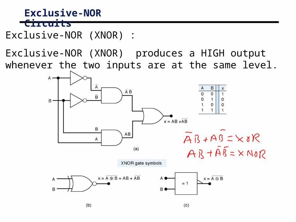
Exclusive-NOR (XNOR) :
Exclusive-NOR (XNOR) produces a HIGH output whenever the two inputs are at the same level.
Exclusive-NOR Circuits

XNOR gate may be used to simplify circuit implementation.
Exclusive-NOR Circuits

XOR Function° XOR function can also be implemented with AND/OR gates (also NANDs).

FIGURE 4-25 XOR gates used to implement the parity generator and the parity checker for an even-parity system.
Parity Generation and Checking

Summary
° Follow rules to convert between AND/OR representation and symbols
° Conversions are based on DeMorgan’s Law
° NOR gate implementations are also possible
° XORs provide straightforward implementation for some functions
° Used for parity generation and checking• XOR circuits could also be implemented using AND/Ors
° Next time: Hazards
Related Documents