1/26 VHDL VHDL Structural Modeling Digital Logic

Welcome message from author
This document is posted to help you gain knowledge. Please leave a comment to let me know what you think about it! Share it to your friends and learn new things together.
Transcript
1/26
VHDL VHDL Structural Modeling
Digital Logic
2/26
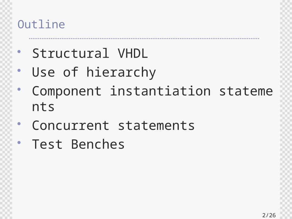
Outline
Structural VHDL Use of hierarchy Component instantiation statements
Concurrent statements Test Benches
3/26
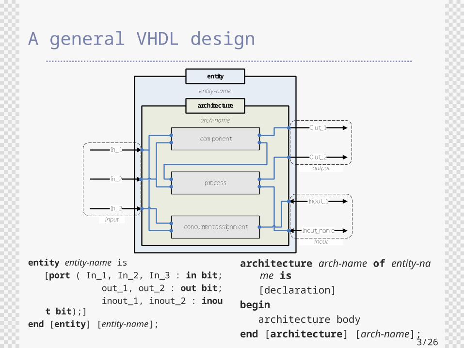
A general VHDL design
output
entity
architecture
entity-name
Out_1
Out_2
inoutInout_nam e
input
In_1
In_2
In_3
arch-name
com ponent
process
concurrent assignm ent
Inout_1
entity entity-name is [port ( In_1, In_2, In_3 : in bit; out_1, out_2 : out bit; inout_1, inout_2 : inou
t bit);] end [entity] [entity-name];
architecture arch-name of entity-name is
[declaration]begin architecture bodyend [architecture] [arch-name];
4/26
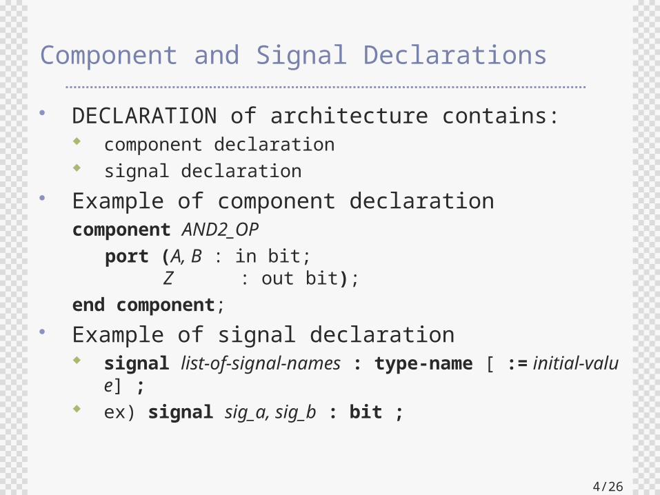
Component and Signal Declarations
DECLARATION of architecture contains: component declaration signal declaration
Example of component declarationcomponent AND2_OP port (A, B : in bit;
Z : out bit);end component;
Example of signal declaration signal list-of-signal-names : type-name [ := initial-valu
e] ; ex) signal sig_a, sig_b : bit ;
5/26
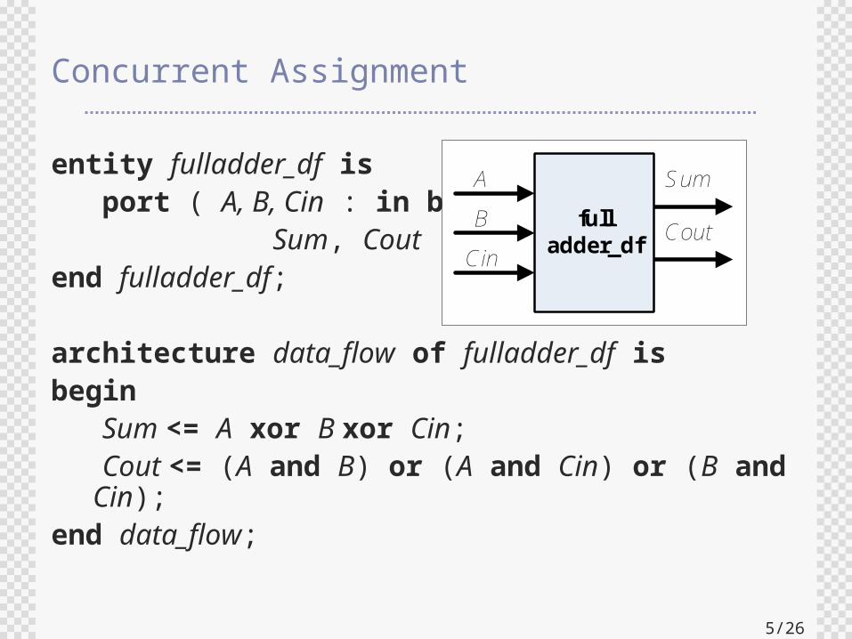
Concurrent Assignment
entity fulladder_df is port ( A, B, Cin : in bit; Sum, Cout : out bit);end fulladder_df;
architecture data_flow of fulladder_df isbegin Sum <= A xor B xor Cin; Cout <= (A and B) or (A and Cin) or (B and
Cin); end data_flow;
ABC in
fulladder_df
S um
Cout
6/26
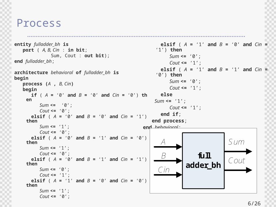
Processentity fulladder_bh is port ( A, B, Cin : in bit; Sum, Cout : out bit);end fulladder_bh;
architecture behavioral of fulladder_bh isbegin process (A , B, Cin) begin if ( A = ‘0’ and B = ‘0’ and Cin = ‘0’) th
en Sum <= ‘0’; Cout <= ‘0’; elsif ( A = ‘0’ and B = ‘0’ and Cin = ‘1’)
then Sum <= ‘1’; Cout <= ‘0’; elsif ( A = ‘0’ and B = ‘1’ and Cin = ‘0’)
then Sum <= ‘1’; Cout <= ‘0’; elsif ( A = ‘0’ and B = ‘1’ and Cin = ‘1’)
then Sum <= ‘0’; Cout <= ‘1’; elsif ( A = ‘1’ and B = ‘0’ and Cin = ‘0’)
then Sum <= ‘1’; Cout <= ‘0’;
elsif ( A = ‘1’ and B = ‘0’ and Cin = ‘1’) then
Sum <= ‘0’; Cout <= ‘1’; elsif ( A = ‘1’ and B = ‘1’ and Cin =
‘0’) then Sum <= ‘0’; Cout <= ‘1’; else Sum <= ‘1’; Cout <= ‘1’; end if; end process;end behavioral;
ABC in
fulladder_bh
S um
Cout
7/26
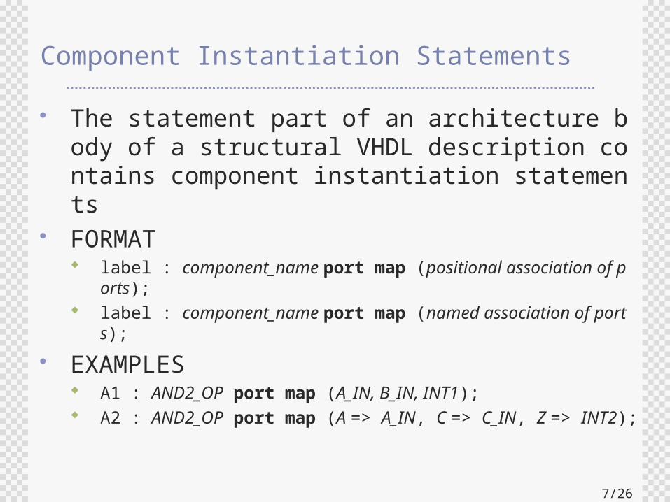
Component Instantiation Statements
The statement part of an architecture body of a structural VHDL description contains component instantiation statements
FORMAT label : component_name port map (positional association of p
orts); label : component_name port map (named association of port
s); EXAMPLES
A1 : AND2_OP port map (A_IN, B_IN, INT1); A2 : AND2_OP port map (A => A_IN, C => C_IN, Z => INT2);
8/26
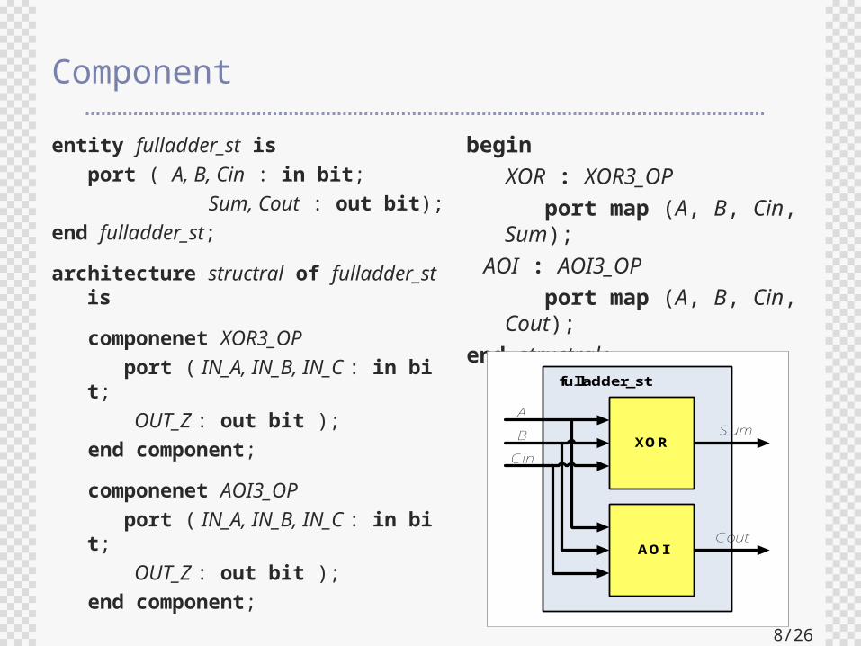
Component
entity fulladder_st is port ( A, B, Cin : in bit; Sum, Cout : out bit);end fulladder_st;
architecture structral of fulladder_st is
componenet XOR3_OP port ( IN_A, IN_B, IN_C : in bi
t; OUT_Z : out bit ); end component;
componenet AOI3_OP port ( IN_A, IN_B, IN_C : in bi
t; OUT_Z : out bit ); end component;
begin XOR : XOR3_OP port map (A, B, Cin,
Sum); AOI : AOI3_OP port map (A, B, Cin,
Cout);end structral;
ABC in
XORS um
AOICout
fulladder_st
9/26
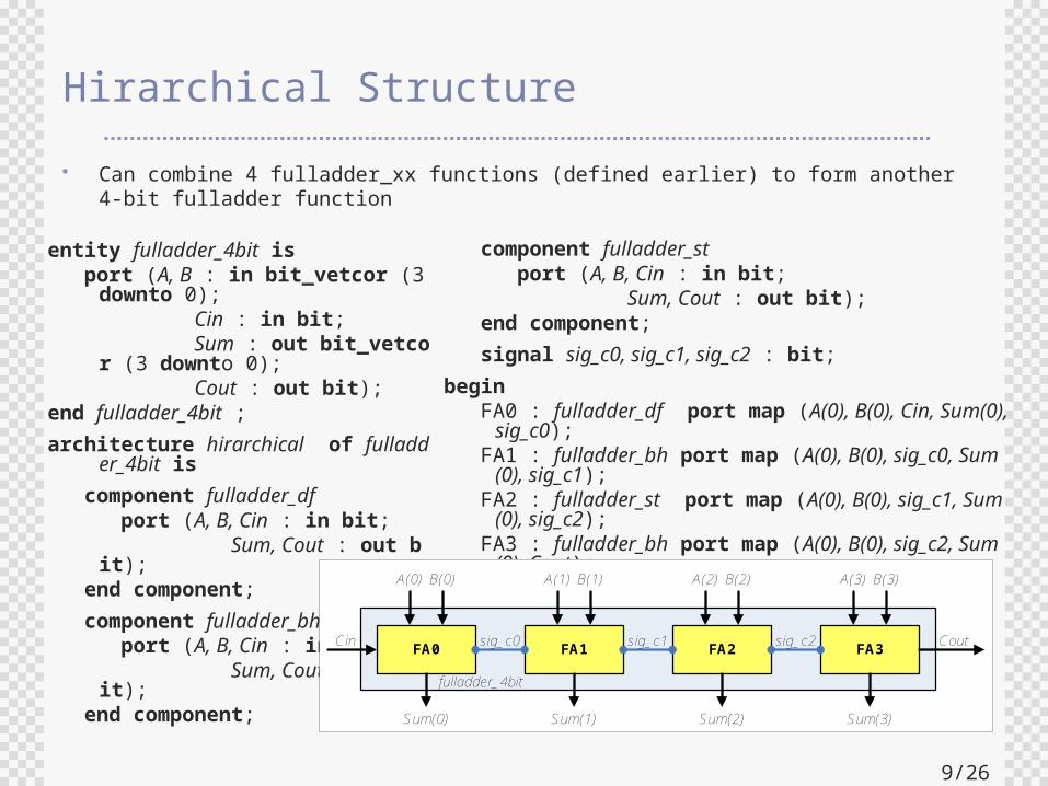
Hirarchical Structure Can combine 4 fulladder_xx functions (defined earlier) to form another
4-bit fulladder function
component fulladder_st port (A, B, Cin : in bit; Sum, Cout : out bit); end component; signal sig_c0, sig_c1, sig_c2 : bit;begin FA0 : fulladder_df port map (A(0), B(0), Cin, Sum(0),
sig_c0); FA1 : fulladder_bh port map (A(0), B(0), sig_c0, Sum
(0), sig_c1); FA2 : fulladder_st port map (A(0), B(0), sig_c1, Sum
(0), sig_c2); FA3 : fulladder_bh port map (A(0), B(0), sig_c2, Sum
(0), Cout);end hirarchical;
entity fulladder_4bit is port (A, B : in bit_vetcor (3
downto 0); Cin : in bit; Sum : out bit_vetco
r (3 downto 0); Cout : out bit);end fulladder_4bit ;architecture hirarchical of fulladd
er_4bit is component fulladder_df port (A, B, Cin : in bit; Sum, Cout : out b
it); end component; component fulladder_bh port (A, B, Cin : in bit; Sum, Cout : out b
it); end component;
FA0 FA1 FA2 FA3
B(3)A (3)B(2)A (2)B(1)A (1)B(0)A (0)
C in Cout
S um(3)S um(2)S um(1)S um(0)
sig_ c0 sig_ c1 sig_ c2
fulladder_ 4bit
10/26
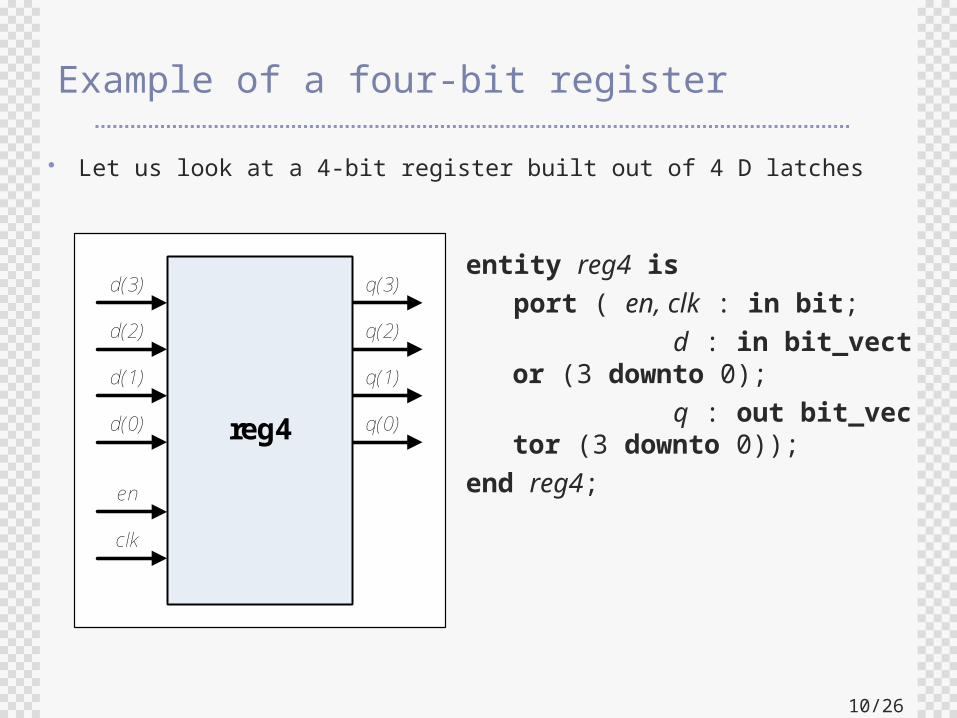
Example of a four-bit register
reg4
d(3)
d(2)
d(1)
d(0)
en
clk
q(3)
q(2)
q(1)
q(0)
entity reg4 is port ( en, clk : in bit; d : in bit_vect
or (3 downto 0); q : out bit_vec
tor (3 downto 0));end reg4;
Let us look at a 4-bit register built out of 4 D latches
11/26
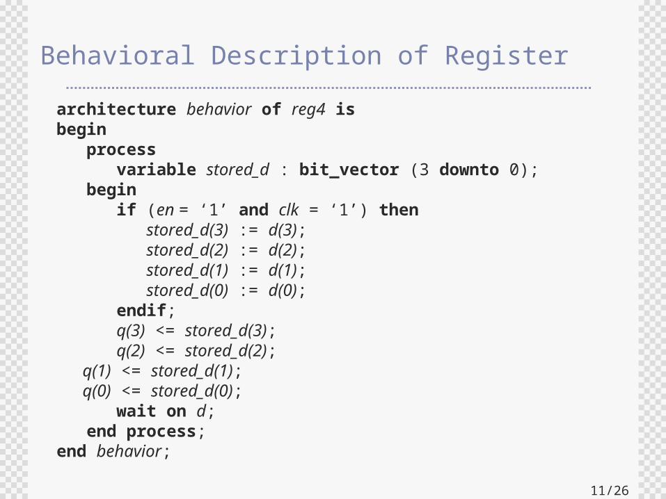
Behavioral Description of Registerarchitecture behavior of reg4 isbegin process variable stored_d : bit_vector (3 downto 0); begin if (en = ‘1’ and clk = ‘1’) then stored_d(3) := d(3); stored_d(2) := d(2); stored_d(1) := d(1); stored_d(0) := d(0); endif; q(3) <= stored_d(3); q(2) <= stored_d(2); q(1) <= stored_d(1); q(0) <= stored_d(0); wait on d; end process;end behavior;
12/26
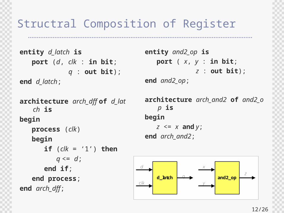
Structral Composition of Register
entity d_latch is port (d, clk : in bit; q : out bit);end d_latch;
architecture arch_dff of d_latch is
begin process (clk) begin if (clk = ‘1’) then q <= d; end if; end process;end arch_dff;
entity and2_op is port ( x, y : in bit; z : out bit);end and2_op;
architecture arch_and2 of and2_op is
begin z <= x and y;end arch_and2;
d
clkd_latch q
x
yand2_op
z
13/26
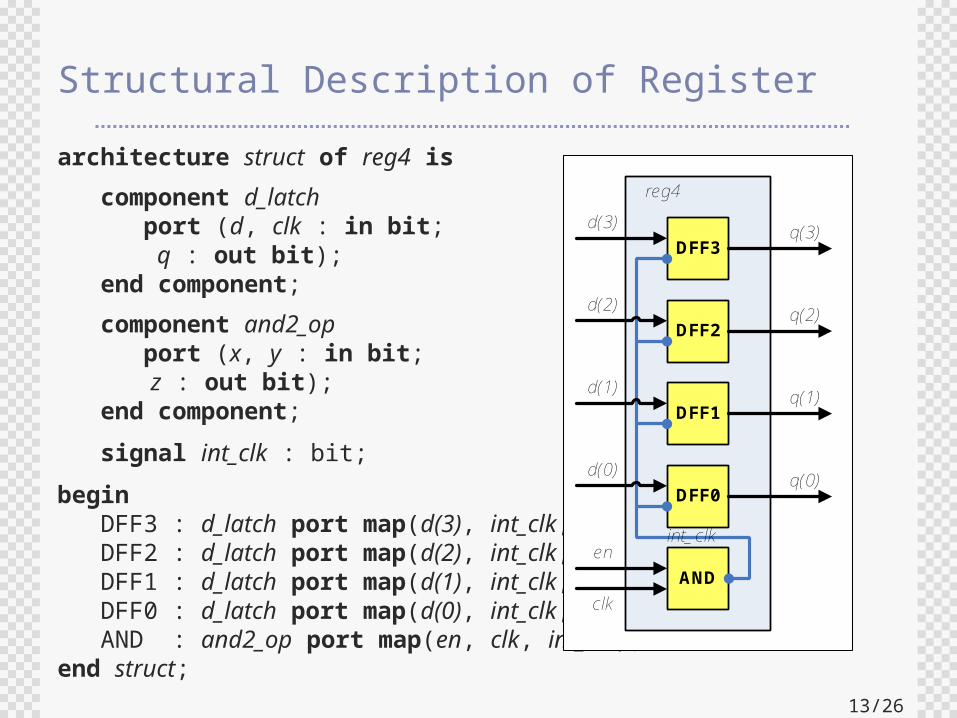
Structural Description of Registerarchitecture struct of reg4 is component d_latch port (d, clk : in bit; q : out bit); end component; component and2_op port (x, y : in bit; z : out bit); end component; signal int_clk : bit;begin DFF3 : d_latch port map(d(3), int_clk, q(3)); DFF2 : d_latch port map(d(2), int_clk, q(2)); DFF1 : d_latch port map(d(1), int_clk, q(1)); DFF0 : d_latch port map(d(0), int_clk, q(0)); AND : and2_op port map(en, clk, int_clk);end struct;
d(3)
d(1)
q(3)
DFF2
DFF1
DFF0
DFF3
d(2)
d(0)
en
clkAND
q(2)
q(1)
q(0)
reg4
int_ clk
14/26
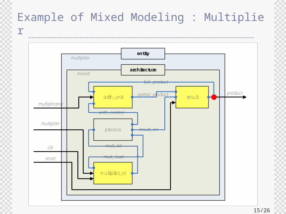
Mixed Models
Models need not be purely structural or behavioral
Often it is useful to specify a model with some parts composed of interconnected component instances and other parts using processes
Use signals as a way to join component instances and processes
A signal can be associated with a port of a component instance and can be assigned to or read in a process
15/26
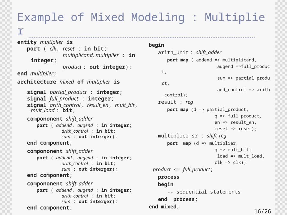
Example of Mixed Modeling : Multiplier
product
entity
architecture
multiplier
mixed
arith_unit
m ultiplier_sr
clk
reset
multiplicand
multiplierprocess
resultpartial_ product
full_ product
arith_ control
mult_ bit
mult_ load
result_ en
16/26
Example of Mixed Modeling : Multiplierentity multiplier is port ( clk, reset : in bit; multiplicand, multiplier : in
integer; product : out integer);end multiplier;architecture mixed of multiplier is signal partial_product : integer; signal full_product : integer; signal arith_control, result_en, mult_bit,
mult_load : bit; compononent shift_adder port ( addend, augend : in integer; arith_control : in bit; sum : out interger); end component;
compononent shift_adder port ( addend, augend : in integer; arith_control : in bit; sum : out interger); end component;
compononent shift_adder port ( addend, augend : in integer; arith_control : in bit; sum : out interger); end component;
begin arith_unit : shift_adder port map ( addend => multiplicand, augend =>full_produc
t, sum => partial_produ
ct, add_control => arith
_control); result : reg port map (d => partial_product, q => full_product, en => result_en, reset => reset); multiplier_sr : shift_reg port map (d => multiplier, q => mult_bit, load => mult_load, clk => clk); product <= full_product; process begin -- sequential statements end process;end mixed;
17/26
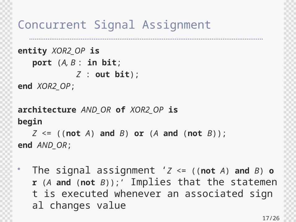
Concurrent Signal Assignment
entity XOR2_OP is port (A, B : in bit; Z : out bit);end XOR2_OP;
architecture AND_OR of XOR2_OP isbegin Z <= ((not A) and B) or (A and (not B));end AND_OR;
The signal assignment ‘Z <= ((not A) and B) or (A and (not B));’ Implies that the statement is executed whenever an associated signal changes value
18/26
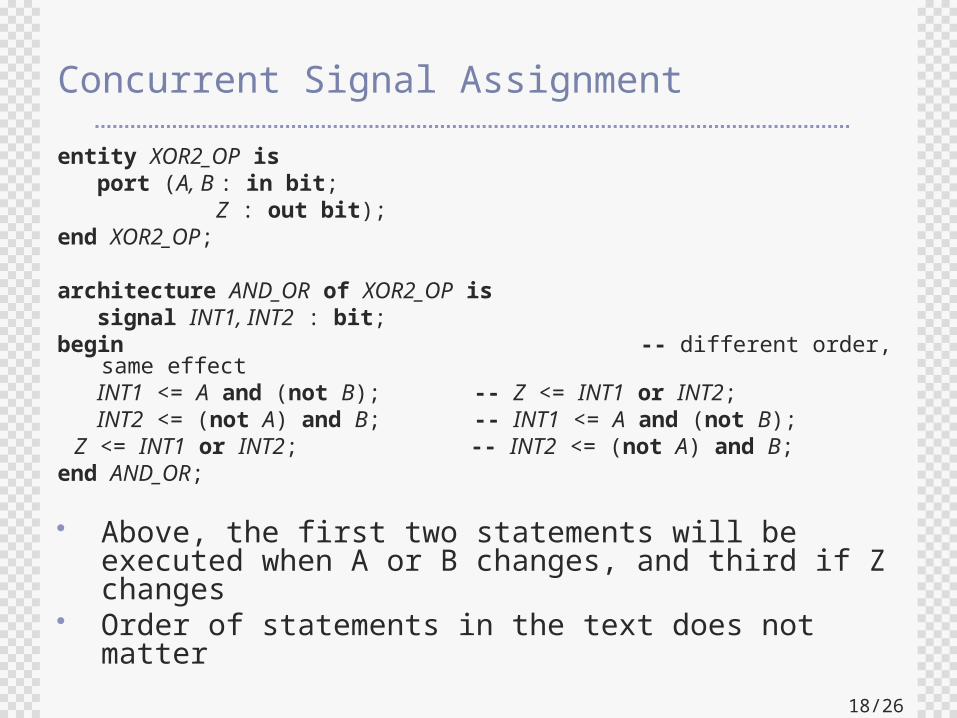
Concurrent Signal Assignmententity XOR2_OP is port (A, B : in bit; Z : out bit);end XOR2_OP;
architecture AND_OR of XOR2_OP is signal INT1, INT2 : bit;begin -- different order,
same effect INT1 <= A and (not B); -- Z <= INT1 or INT2; INT2 <= (not A) and B; -- INT1 <= A and (not B); Z <= INT1 or INT2; -- INT2 <= (not A) and B;end AND_OR;
Above, the first two statements will be executed when A or B changes, and third if Z changes
Order of statements in the text does not matter
19/26
Concurrent and Sequential Statements
VHDL provide both concurrent and sequential signal assignments
Example SIG_A <= IN_A and IN_B; SIG_B <= IN_A nor IN_C; SIG_C <= not IN_D;
The above sequence of statements can be concurrent or sequential depending on context
If above appears inside an architecture body, it is a concurrent signal assignment
If above appears inside a process statement, they will be executed sequentially
20/26
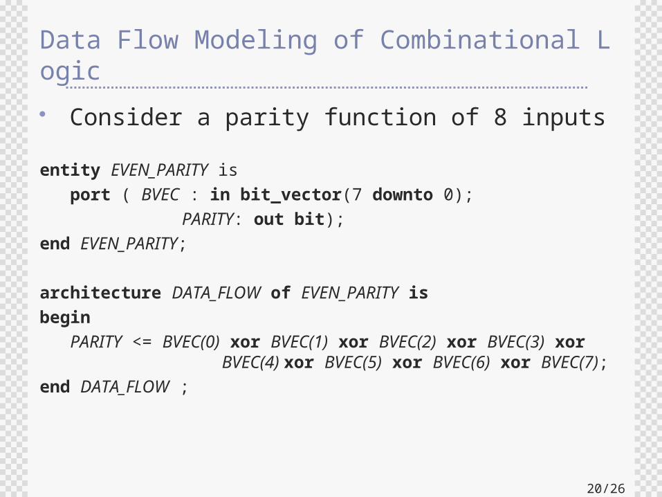
Data Flow Modeling of Combinational Logic Consider a parity function of 8 inputs
entity EVEN_PARITY is port ( BVEC : in bit_vector(7 downto 0); PARITY: out bit);end EVEN_PARITY;
architecture DATA_FLOW of EVEN_PARITY isbegin PARITY <= BVEC(0) xor BVEC(1) xor BVEC(2) xor BVEC(3) xor
BVEC(4) xor BVEC(5) xor BVEC(6) xor BVEC(7);end DATA_FLOW ;
21/26
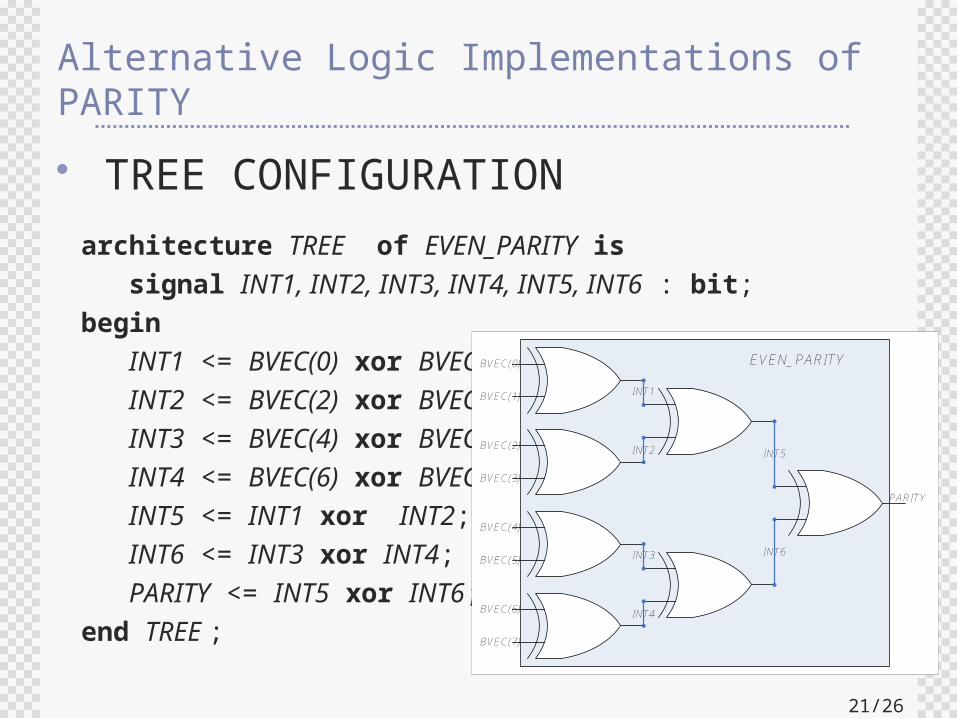
Alternative Logic Implementations of PARITY TREE CONFIGURATIONarchitecture TREE of EVEN_PARITY is signal INT1, INT2, INT3, INT4, INT5, INT6 : bit;begin INT1 <= BVEC(0) xor BVEC(1) ; INT2 <= BVEC(2) xor BVEC(3) ; INT3 <= BVEC(4) xor BVEC(5) ; INT4 <= BVEC(6) xor BVEC(7) ; INT5 <= INT1 xor INT2; INT6 <= INT3 xor INT4; PARITY <= INT5 xor INT6;end TREE ;
BVEC (0)
BVEC (1)
BVEC (2)
BVEC (3)
BVEC (4)
BVEC (5)
BVEC (6)
BVEC (7)
INT1
INT2
INT3
INT4
INT5
INT6
PAR ITY
EVEN_ PAR ITY
22/26
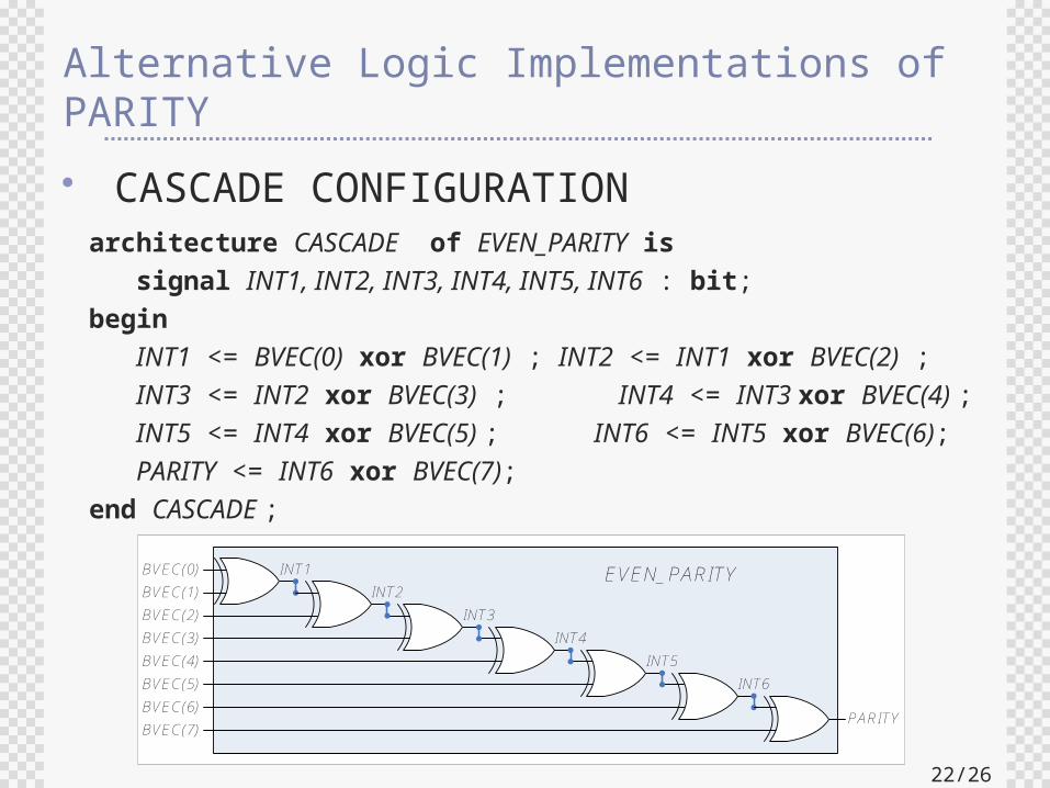
Alternative Logic Implementations of PARITY CASCADE CONFIGURATIONarchitecture CASCADE of EVEN_PARITY is signal INT1, INT2, INT3, INT4, INT5, INT6 : bit;begin INT1 <= BVEC(0) xor BVEC(1) ; INT2 <= INT1 xor BVEC(2) ; INT3 <= INT2 xor BVEC(3) ; INT4 <= INT3 xor BVEC(4) ; INT5 <= INT4 xor BVEC(5) ; INT6 <= INT5 xor BVEC(6); PARITY <= INT6 xor BVEC(7);end CASCADE ;
BVEC (0)BVEC (1)BVEC (2)BVEC (3)BVEC (4)BVEC (5)BVEC (6)BVEC (7)
INT1INT2
PAR ITY
EVEN_ PAR ITY
INT3INT4
INT6INT5
23/26
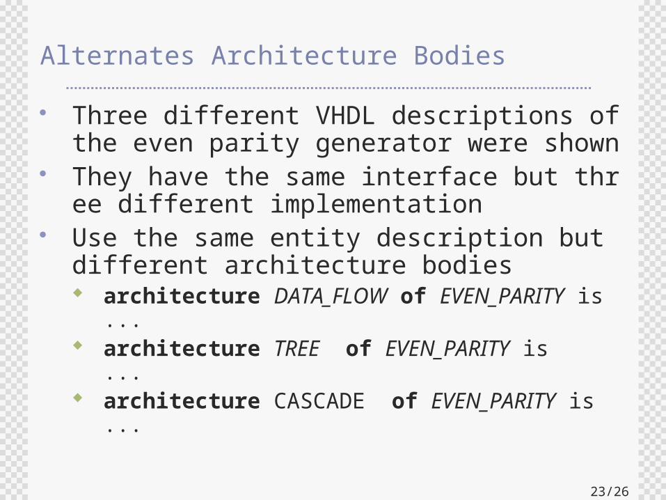
Alternates Architecture Bodies
Three different VHDL descriptions of the even parity generator were shown
They have the same interface but three different implementation
Use the same entity description but different architecture bodies architecture DATA_FLOW of EVEN_PARITY is
... architecture TREE of EVEN_PARITY is
... architecture CASCADE of EVEN_PARITY is
...
24/26
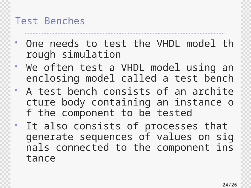
Test Benches
One needs to test the VHDL model through simulation
We often test a VHDL model using an enclosing model called a test bench
A test bench consists of an architecture body containing an instance of the component to be tested
It also consists of processes that generate sequences of values on signals connected to the component instance
25/26
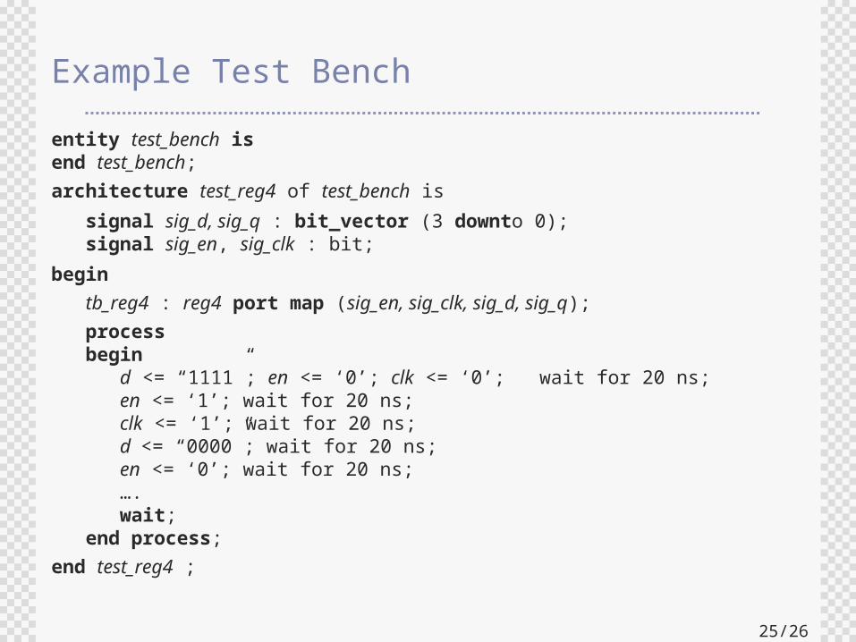
Example Test Benchentity test_bench isend test_bench;architecture test_reg4 of test_bench is signal sig_d, sig_q : bit_vector (3 downto 0); signal sig_en, sig_clk : bit;begin tb_reg4 : reg4 port map (sig_en, sig_clk, sig_d, sig_q);
process begin d <= “1111”; en <= ‘0’; clk <= ‘0’; wait for 20 ns; en <= ‘1’; wait for 20 ns; clk <= ‘1’; wait for 20 ns; d <= “0000”; wait for 20 ns; en <= ‘0’; wait for 20 ns; …. wait; end process;end test_reg4 ;
26/26
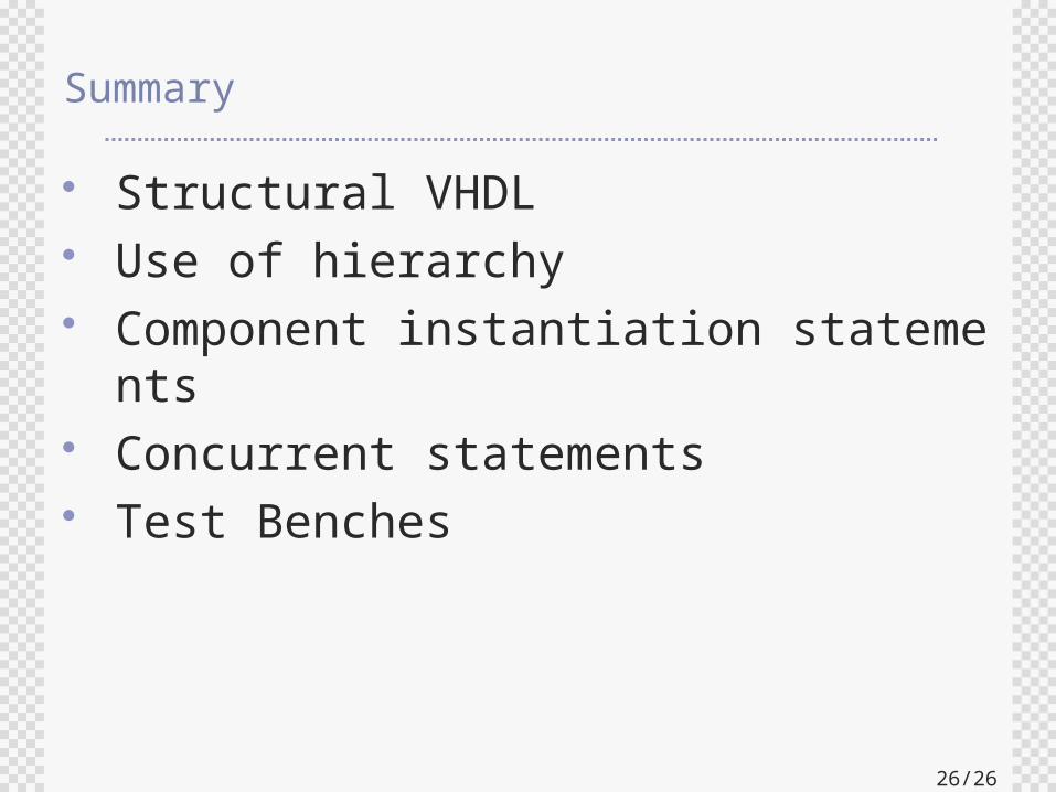
Summary
Structural VHDL Use of hierarchy Component instantiation statements
Concurrent statements Test Benches
Related Documents