Leaded MLCC for Automotive with AEC-Q200 RCE Series Reference Specification Product specifications in this catalog are as of Dec. 2017, and are subject to change or obsolescence without notice. Please consult the approval sheet before ordering.Please read rating and Cautions first.

Welcome message from author
This document is posted to help you gain knowledge. Please leave a comment to let me know what you think about it! Share it to your friends and learn new things together.
Transcript

Leaded MLCC for Automotive with AEC-Q200
RCE Series
Reference Specification
Product specifications in this catalog are as of Dec. 2017, and are subject to change or obsolescence without notice. Please consult the approval sheet before ordering.Please read rating and Cautions first.

Reference only
EGLEDMNO03 1 / 19
CAUTION 1. OPERATING VOLTAGE
When DC-rated capacitors are to be used in AC or ripple current circuits, be sure to maintain the Vp-p value of the applied voltage or the Vo-p which contains DC bias within the rated voltage range. When the voltage is started to apply to the circuit or it is stopped applying, the irregular voltage may be generated for a transit period because of resonance or switching. Be sure to use a capacitor within rated voltage containing these irregular voltage. When DC-rated capacitors are to be used in input circuits from commercial power source (AC filter), be sure to use Safety Recognized Capacitors because various regulations on withstand voltage or impulse withstand established for each equipment should be taken into considerations.
Voltage DC Voltage DC+AC Voltage AC Voltage Pulse Voltage(1) Pulse Voltage(2)
Positional Measurement
2. OPERATING TEMPERATURE AND SELF-GENERATED HEAT Keep the surface temperature of a capacitor below the upper limit of its rated operating temperature range. Be sure to take into account the heat generated by the capacitor itself. When the capacitor is used in a high-frequency current, pulse current or the like, it may have the self- generated heat due to dielectric-loss. In case of Class 2 capacitors (Temp.Char. : X7R,X7S,X8L, etc.), applied voltage should be the load such as self-generated heat is within 20 C on the condition of atmosphere temperature 25 C. Please contact us if self-generated heat is occurred with Class 1 capacitors (Temp.Char. : C0G,U2J,X8G, etc.). When measuring, use a thermocouple of small thermal capacity-K of 0.1mm and be in the condition where capacitor is not affected by radiant heat of other components and wind of surroundings. Excessive heat may lead to deterioration of the capacitor’s characteristics and reliability.
3. Fail-safe Be sure to provide an appropriate fail-safe function on your product to prevent a second damage that may be caused by the abnormal function or the failure of our product.
4. OPERATING AND STORAGE ENVIRONMENT The insulating coating of capacitors does not form a perfect seal; therefore, do not use or store capacitors in a corrosive atmosphere, especially where chloride gas, sulfide gas, acid, alkali, salt or the like are present. And avoid exposure to moisture. Before cleaning, bonding, or molding this product, verify that these processes do not affect product quality by testing the performance of a cleaned, bonded or molded product in the intended equipment. Store the capacitors where the temperature and relative humidity do not exceed 5 to 40 C and 20 to 70%. Use capacitors within 6 months.
5. VIBRATION AND IMPACT Do not expose a capacitor or its leads to excessive shock or vibration during use.
6. SOLDERING When soldering this product to a PCB/PWB, do not exceed the solder heat resistance specification of the capacitor. Subjecting this product to excessive heating could melt the internal junction solder and may result in thermal shocks that can crack the ceramic element.
7. BONDING AND RESIN MOLDING, RESIN COAT In case of bonding, molding or coating this product, verify that these processes do not affect the quality of capacitor by testing the performance of a bonded or molded product in the intended equipment. In case of the amount of applications, dryness / hardening conditions of adhesives and molding resins containing organic solvents (ethyl acetate, methyl ethyl ketone, toluene, etc.) are unsuitable, the outer coating resin of a capacitor is damaged by the organic solvents and it may result, worst case, in a short circuit. The variation in thickness of adhesive or molding resin may cause a outer coating resin cracking and/or ceramic element cracking of a capacitor in a temperature cycling.
8. TREATMENT AFTER BONDING AND RESIN MOLDING, RESIN COAT When the outer coating is hot (over 100 C) after soldering, it becomes soft and fragile. So please be careful not to give it mechanical stress.
Vp-p Vp-pVp-pVo-p Vo-p
Reference only
EGLEDMNO03 2 / 19
Failure to follow the above cautions may result, worst case, in a short circuit and cause fuming or partial dispersion when the product is used.
9. LIMITATION OF APPLICATIONS
Please contact us before using our products for the applications listed below which require especially high reliability for the prevention of defects which might directly cause damage to the third party’s life, body or property.
1. Aircraft equipment 2. Aerospace equipment 3. Undersea equipment 4. Power plant control equipment 5. Medical equipment 6. Transportation equipment (vehicles, trains, ships, etc.) 7. Traffic signal equipment 8. Disaster prevention / crime prevention equipment 9. Data-processing equipment exerting influence on public 10. Application of similar complexity and/or reliability requirements to the applications listed in the above.
NOTICE 1. CLEANING (ULTRASONIC CLEANING)
To perform ultrasonic cleaning, observe the following conditions. Rinse bath capacity : Output of 20 watts per liter or less. Rinsing time : 5 min maximum. Do not vibrate the PCB/PWB directly. Excessive ultrasonic cleaning may lead to fatigue destruction of the lead wires.
2. Soldering and Mounting
Insertion of the Lead Wire • When soldering, insert the lead wire into the PCB without mechanically stressing the lead wire. • Insert the lead wire into the PCB with a distance appropriate to the lead space.
3. CAPACITANCE CHANGE OF CAPACITORS
• Class 2 capacitors (Temp.Char. : X7R,X7S,X8L, etc.) Class 2 capacitors an aging characteristic, whereby the capacitor continually decreases its capacitance slightly if the capacitor leaves for a long time. Moreover, capacitance might change greatly depending on a surrounding temperature or an applied voltage. So, it is not likely to be able to use for the time constant circuit. Please contact us if you need a detail information.
NOTE 1. Please make sure that your product has been evaluated in view of your specifications with our product
being mounted to your product. 2. You are requested not to use our product deviating from this specification.
Reference only
ETRCE01D 3 / 19
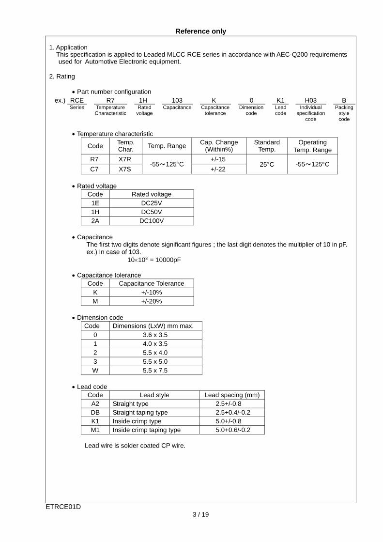
1. Application This specification is applied to Leaded MLCC RCE series in accordance with AEC-Q200 requirements
used for Automotive Electronic equipment. 2. Rating Part number configuration
ex.) RCE R7 1H 103 K 0 K1 H03 B Series Temperature
Characteristic Rated
voltage Capacitance Capacitance
toleranceDimension
code Lead code
Individualspecification
code
Packingstyle code
Temperature characteristic
Code Temp. Char. Temp. Range Cap. Change
(Within%) Standard
Temp. Operating
Temp. Range
R7 X7R -55~125C
+/-15 25C -55~125C
C7 X7S +/-22 Rated voltage
Code Rated voltage 1E DC25V 1H DC50V 2A DC100V
Capacitance The first two digits denote significant figures ; the last digit denotes the multiplier of 10 in pF. ex.) In case of 103. 10103 = 10000pF Capacitance tolerance
Code Capacitance Tolerance K +/-10% M +/-20%
Dimension code
Code Dimensions (LxW) mm max. 0 3.6 x 3.5 1 4.0 x 3.5 2 5.5 x 4.0 3 5.5 x 5.0 W 5.5 x 7.5
Lead code
Code Lead style Lead spacing (mm)A2 Straight type 2.5+/-0.8 DB Straight taping type 2.5+0.4/-0.2 K1 Inside crimp type 5.0+/-0.8 M1 Inside crimp taping type 5.0+0.6/-0.2
Lead wire is solder coated CP wire.

Reference only
ETRCE01D 4 / 19
Individual specification code Murata’s control code Please refer to Part number list . Packing style code
Code Packing style A Taping type of Ammo B Bulk type
3. Marking Temp. char. : Letter code : C (X7R/X7S Char. Except dimension code : 0,1) Capacitance : 3 digit numbers Capacitance tolerance : Code Rated voltage : Letter code : 2 (DC25V only.) Letter code : 5 (DC50V only. Except dimension code : 0,1) Letter code : 1 (DC100V only. Except dimension code : 0,1) Company name code : Abbreviation : (Except dimension code : 0,1)
(Ex.)
Rated voltage
Dimension code 25V 50V 100V
0,1
2
3,W
103K 104K
335K5C
225 K1C
226M2C
475K2C
105K5C
105 K1C
105K

Reference only
5 / 19
4. Part number list
Unit : mm
Customer Part Number Murata Part Number T.C.
DC Rated Volt. (V)
Cap.Cap. tol.
Dimension (mm) Size Lead Code
Pack qty.
(pcs)L W W1 F T
RCER71E104K0A2H03B X7R 25 0.1µF ±10% 3.6 3.5 - 2.5 2.5 0A2 500
RCER71E154K0A2H03B X7R 25 0.15µF ±10% 3.6 3.5 - 2.5 2.5 0A2 500
RCER71E224K0A2H03B X7R 25 0.22µF ±10% 3.6 3.5 - 2.5 2.5 0A2 500
RCER71E334K1A2H03B X7R 25 0.33µF ±10% 4.0 3.5 - 2.5 2.5 1A2 500
RCER71E474K1A2H03B X7R 25 0.47µF ±10% 4.0 3.5 - 2.5 2.5 1A2 500
RCER71E684K1A2H03B X7R 25 0.68µF ±10% 4.0 3.5 - 2.5 2.5 1A2 500
RCER71E105K1A2H03B X7R 25 1.0µF ±10% 4.0 3.5 - 2.5 2.5 1A2 500
RCER71E155K2A2H03B X7R 25 1.5µF ±10% 5.5 4.0 - 2.5 3.15 2A2 500
RCER71E225K2A2H03B X7R 25 2.2µF ±10% 5.5 4.0 - 2.5 3.15 2A2 500
RCER71E335K2A2H03B X7R 25 3.3µF ±10% 5.5 4.0 - 2.5 3.15 2A2 500
RCER71E475K2A2H03B X7R 25 4.7µF ±10% 5.5 4.0 - 2.5 3.15 2A2 500
RCER71E106K3A2H03B X7R 25 10µF ±10% 5.5 5.0 - 2.5 4.0 3A2 500
RCER71H221K0A2H03B X7R 50 220pF ±10% 3.6 3.5 - 2.5 2.5 0A2 500
RCER71H331K0A2H03B X7R 50 330pF ±10% 3.6 3.5 - 2.5 2.5 0A2 500
RCER71H471K0A2H03B X7R 50 470pF ±10% 3.6 3.5 - 2.5 2.5 0A2 500
RCER71H681K0A2H03B X7R 50 680pF ±10% 3.6 3.5 - 2.5 2.5 0A2 500
RCER71H102K0A2H03B X7R 50 1000pF ±10% 3.6 3.5 - 2.5 2.5 0A2 500
RCER71H152K0A2H03B X7R 50 1500pF ±10% 3.6 3.5 - 2.5 2.5 0A2 500
RCER71H222K0A2H03B X7R 50 2200pF ±10% 3.6 3.5 - 2.5 2.5 0A2 500
RCER71H332K0A2H03B X7R 50 3300pF ±10% 3.6 3.5 - 2.5 2.5 0A2 500
RCER71H472K0A2H03B X7R 50 4700pF ±10% 3.6 3.5 - 2.5 2.5 0A2 500
RCER71H682K0A2H03B X7R 50 6800pF ±10% 3.6 3.5 - 2.5 2.5 0A2 500
RCER71H103K0A2H03B X7R 50 10000pF ±10% 3.6 3.5 - 2.5 2.5 0A2 500
RCER71H153K0A2H03B X7R 50 15000pF ±10% 3.6 3.5 - 2.5 2.5 0A2 500
RCER71H223K0A2H03B X7R 50 22000pF ±10% 3.6 3.5 - 2.5 2.5 0A2 500
RCER71H333K0A2H03B X7R 50 33000pF ±10% 3.6 3.5 - 2.5 2.5 0A2 500
RCER71H473K0A2H03B X7R 50 47000pF ±10% 3.6 3.5 - 2.5 2.5 0A2 500
RCER71H683K0A2H03B X7R 50 68000pF ±10% 3.6 3.5 - 2.5 2.5 0A2 500
RCER71H104K0A2H03B X7R 50 0.1µF ±10% 3.6 3.5 - 2.5 2.5 0A2 500
RCER71H154K1A2H03B X7R 50 0.15µF ±10% 4.0 3.5 - 2.5 2.5 1A2 500
RCER71H224K1A2H03B X7R 50 0.22µF ±10% 4.0 3.5 - 2.5 2.5 1A2 500
RCER71H334K1A2H03B X7R 50 0.33µF ±10% 4.0 3.5 - 2.5 2.5 1A2 500
RCER71H474K1A2H03B X7R 50 0.47µF ±10% 4.0 3.5 - 2.5 2.5 1A2 500
RCER71H684K2A2H03B X7R 50 0.68µF ±10% 5.5 4.0 - 2.5 3.15 2A2 500
RCEC71H105K1A2H03B X7S 50 1.0µF ±10% 4.0 3.5 - 2.5 2.5 1A2 500
RCER71H105K2A2H03B X7R 50 1.0µF ±10% 5.5 4.0 - 2.5 3.15 2A2 500
RCER71H155K2A2H03B X7R 50 1.5µF ±10% 5.5 4.0 - 2.5 3.15 2A2 500
RCER71H225K2A2H03B X7R 50 2.2µF ±10% 5.5 4.0 - 2.5 3.15 2A2 500
RCER71H335K3A2H03B X7R 50 3.3µF ±10% 5.5 5.0 - 2.5 4.0 3A2 500

Reference only
6 / 19
Unit : mm
Customer Part Number Murata Part Number T.C.
DC Rated Volt. (V)
Cap.Cap. tol.
Dimension (mm) Size Lead Code
Pack qty.
(pcs)L W W1 F T
RCEC71H475K2A2H03B X7S 50 4.7µF ±10% 5.5 4.0 - 2.5 3.15 2A2 500
RCER71H475K3A2H03B X7R 50 4.7µF ±10% 5.5 5.0 - 2.5 4.0 3A2 500
RCEC71H106K3A2H03B X7S 50 10µF ±10% 5.5 5.0 - 2.5 4.0 3A2 500
RCER72A221K0A2H03B X7R 100 220pF ±10% 3.6 3.5 - 2.5 2.5 0A2 500
RCER72A331K0A2H03B X7R 100 330pF ±10% 3.6 3.5 - 2.5 2.5 0A2 500
RCER72A471K0A2H03B X7R 100 470pF ±10% 3.6 3.5 - 2.5 2.5 0A2 500
RCER72A681K0A2H03B X7R 100 680pF ±10% 3.6 3.5 - 2.5 2.5 0A2 500
RCER72A102K0A2H03B X7R 100 1000pF ±10% 3.6 3.5 - 2.5 2.5 0A2 500
RCER72A152K0A2H03B X7R 100 1500pF ±10% 3.6 3.5 - 2.5 2.5 0A2 500
RCER72A222K0A2H03B X7R 100 2200pF ±10% 3.6 3.5 - 2.5 2.5 0A2 500
RCER72A332K0A2H03B X7R 100 3300pF ±10% 3.6 3.5 - 2.5 2.5 0A2 500
RCER72A472K0A2H03B X7R 100 4700pF ±10% 3.6 3.5 - 2.5 2.5 0A2 500
RCER72A682K0A2H03B X7R 100 6800pF ±10% 3.6 3.5 - 2.5 2.5 0A2 500
RCER72A103K0A2H03B X7R 100 10000pF ±10% 3.6 3.5 - 2.5 2.5 0A2 500
RCER72A153K0A2H03B X7R 100 15000pF ±10% 3.6 3.5 - 2.5 2.5 0A2 500
RCER72A223K0A2H03B X7R 100 22000pF ±10% 3.6 3.5 - 2.5 2.5 0A2 500
RCER72A333K1A2H03B X7R 100 33000pF ±10% 4.0 3.5 - 2.5 2.5 1A2 500
RCER72A473K1A2H03B X7R 100 47000pF ±10% 4.0 3.5 - 2.5 2.5 1A2 500
RCER72A683K1A2H03B X7R 100 68000pF ±10% 4.0 3.5 - 2.5 2.5 1A2 500
RCER72A104K1A2H03B X7R 100 0.1µF ±10% 4.0 3.5 - 2.5 2.5 1A2 500
RCER72A154K2A2H03B X7R 100 0.15µF ±10% 5.5 4.0 - 2.5 3.15 2A2 500
RCER72A224K2A2H03B X7R 100 0.22µF ±10% 5.5 4.0 - 2.5 3.15 2A2 500
RCER72A334K1A2H03B X7R 100 0.33µF ±10% 4.0 3.5 - 2.5 2.5 1A2 500
RCER72A474K2A2H03B X7R 100 0.47µF ±10% 5.5 4.0 - 2.5 3.15 2A2 500
RCER72A684K2A2H03B X7R 100 0.68µF ±10% 5.5 4.0 - 2.5 3.15 2A2 500
RCER72A105K2A2H03B X7R 100 1.0µF ±10% 5.5 4.0 - 2.5 3.15 2A2 500
RCEC72A155K3A2H03B X7S 100 1.5µF ±10% 5.5 5.0 - 2.5 4.0 3A2 500
RCEC72A225K3A2H03B X7S 100 2.2µF ±10% 5.5 5.0 - 2.5 4.0 3A2 500
RCER71E104K0K1H03B X7R 25 0.1µF ±10% 3.6 3.5 6.0 5.0 2.5 0K1 500
RCER71E154K0K1H03B X7R 25 0.15µF ±10% 3.6 3.5 6.0 5.0 2.5 0K1 500
RCER71E224K0K1H03B X7R 25 0.22µF ±10% 3.6 3.5 6.0 5.0 2.5 0K1 500
RCER71E334K1K1H03B X7R 25 0.33µF ±10% 4.0 3.5 5.0 5.0 2.5 1K1 500
RCER71E474K1K1H03B X7R 25 0.47µF ±10% 4.0 3.5 5.0 5.0 2.5 1K1 500
RCER71E684K1K1H03B X7R 25 0.68µF ±10% 4.0 3.5 5.0 5.0 2.5 1K1 500
RCER71E105K1K1H03B X7R 25 1.0µF ±10% 4.0 3.5 5.0 5.0 2.5 1K1 500
RCER71E155K2K1H03B X7R 25 1.5µF ±10% 5.5 4.0 6.0 5.0 3.15 2K1 500
RCER71E225K2K1H03B X7R 25 2.2µF ±10% 5.5 4.0 6.0 5.0 3.15 2K1 500
RCER71E335K2K1H03B X7R 25 3.3µF ±10% 5.5 4.0 6.0 5.0 3.15 2K1 500
RCER71E475K2K1H03B X7R 25 4.7µF ±10% 5.5 4.0 6.0 5.0 3.15 2K1 500
RCER71E106K3K1H03B X7R 25 10µF ±10% 5.5 5.0 7.5 5.0 4.0 3K1 500
RCER71E226MWK1H03B X7R 25 22µF ±20% 5.5 7.5 10.0 5.0 4.0 WK1 500

Reference only
7 / 19
Unit : mm
Customer Part Number Murata Part Number T.C.
DC Rated Volt. (V)
Cap.Cap. tol.
Dimension (mm) Size Lead Code
Pack qty.
(pcs)L W W1 F T
RCER71H221K0K1H03B X7R 50 220pF ±10% 3.6 3.5 6.0 5.0 2.5 0K1 500
RCER71H331K0K1H03B X7R 50 330pF ±10% 3.6 3.5 6.0 5.0 2.5 0K1 500
RCER71H471K0K1H03B X7R 50 470pF ±10% 3.6 3.5 6.0 5.0 2.5 0K1 500
RCER71H681K0K1H03B X7R 50 680pF ±10% 3.6 3.5 6.0 5.0 2.5 0K1 500
RCER71H102K0K1H03B X7R 50 1000pF ±10% 3.6 3.5 6.0 5.0 2.5 0K1 500
RCER71H152K0K1H03B X7R 50 1500pF ±10% 3.6 3.5 6.0 5.0 2.5 0K1 500
RCER71H222K0K1H03B X7R 50 2200pF ±10% 3.6 3.5 6.0 5.0 2.5 0K1 500
RCER71H332K0K1H03B X7R 50 3300pF ±10% 3.6 3.5 6.0 5.0 2.5 0K1 500
RCER71H472K0K1H03B X7R 50 4700pF ±10% 3.6 3.5 6.0 5.0 2.5 0K1 500
RCER71H682K0K1H03B X7R 50 6800pF ±10% 3.6 3.5 6.0 5.0 2.5 0K1 500
RCER71H103K0K1H03B X7R 50 10000pF ±10% 3.6 3.5 6.0 5.0 2.5 0K1 500
RCER71H153K0K1H03B X7R 50 15000pF ±10% 3.6 3.5 6.0 5.0 2.5 0K1 500
RCER71H223K0K1H03B X7R 50 22000pF ±10% 3.6 3.5 6.0 5.0 2.5 0K1 500
RCER71H333K0K1H03B X7R 50 33000pF ±10% 3.6 3.5 6.0 5.0 2.5 0K1 500
RCER71H473K0K1H03B X7R 50 47000pF ±10% 3.6 3.5 6.0 5.0 2.5 0K1 500
RCER71H683K0K1H03B X7R 50 68000pF ±10% 3.6 3.5 6.0 5.0 2.5 0K1 500
RCER71H104K0K1H03B X7R 50 0.1µF ±10% 3.6 3.5 6.0 5.0 2.5 0K1 500
RCER71H154K1K1H03B X7R 50 0.15µF ±10% 4.0 3.5 5.0 5.0 2.5 1K1 500
RCER71H224K1K1H03B X7R 50 0.22µF ±10% 4.0 3.5 5.0 5.0 2.5 1K1 500
RCER71H334K1K1H03B X7R 50 0.33µF ±10% 4.0 3.5 5.0 5.0 2.5 1K1 500
RCER71H474K1K1H03B X7R 50 0.47µF ±10% 4.0 3.5 5.0 5.0 2.5 1K1 500
RCER71H684K2K1H03B X7R 50 0.68µF ±10% 5.5 4.0 6.0 5.0 3.15 2K1 500
RCEC71H105K1K1H03B X7S 50 1.0µF ±10% 4.0 3.5 5.0 5.0 2.5 1K1 500
RCER71H105K2K1H03B X7R 50 1.0µF ±10% 5.5 4.0 6.0 5.0 3.15 2K1 500
RCER71H155K2K1H03B X7R 50 1.5µF ±10% 5.5 4.0 6.0 5.0 3.15 2K1 500
RCER71H225K2K1H03B X7R 50 2.2µF ±10% 5.5 4.0 6.0 5.0 3.15 2K1 500
RCER71H335K3K1H03B X7R 50 3.3µF ±10% 5.5 5.0 7.5 5.0 4.0 3K1 500
RCEC71H475K2K1H03B X7S 50 4.7µF ±10% 5.5 4.0 6.0 5.0 3.15 2K1 500
RCER71H475K3K1H03B X7R 50 4.7µF ±10% 5.5 5.0 7.5 5.0 4.0 3K1 500
RCEC71H106K3K1H03B X7S 50 10µF ±10% 5.5 5.0 7.5 5.0 4.0 3K1 500
RCER71H106MWK1H03B X7R 50 10µF ±20% 5.5 7.5 10.0 5.0 4.0 WK1 500
RCEC71H226MWK1H03B X7S 50 22µF ±20% 5.5 7.5 10.0 5.0 4.0 WK1 500
RCER72A221K0K1H03B X7R 100 220pF ±10% 3.6 3.5 6.0 5.0 2.5 0K1 500
RCER72A331K0K1H03B X7R 100 330pF ±10% 3.6 3.5 6.0 5.0 2.5 0K1 500
RCER72A471K0K1H03B X7R 100 470pF ±10% 3.6 3.5 6.0 5.0 2.5 0K1 500
RCER72A681K0K1H03B X7R 100 680pF ±10% 3.6 3.5 6.0 5.0 2.5 0K1 500
RCER72A102K0K1H03B X7R 100 1000pF ±10% 3.6 3.5 6.0 5.0 2.5 0K1 500
RCER72A152K0K1H03B X7R 100 1500pF ±10% 3.6 3.5 6.0 5.0 2.5 0K1 500
RCER72A222K0K1H03B X7R 100 2200pF ±10% 3.6 3.5 6.0 5.0 2.5 0K1 500
RCER72A332K0K1H03B X7R 100 3300pF ±10% 3.6 3.5 6.0 5.0 2.5 0K1 500

Reference only
8 / 19
Unit : mm
Customer Part Number Murata Part Number T.C.
DC Rated Volt. (V)
Cap.Cap. tol.
Dimension (mm) Size Lead Code
Pack qty.
(pcs)L W W1 F T
RCER72A472K0K1H03B X7R 100 4700pF ±10% 3.6 3.5 6.0 5.0 2.5 0K1 500
RCER72A682K0K1H03B X7R 100 6800pF ±10% 3.6 3.5 6.0 5.0 2.5 0K1 500
RCER72A103K0K1H03B X7R 100 10000pF ±10% 3.6 3.5 6.0 5.0 2.5 0K1 500
RCER72A153K0K1H03B X7R 100 15000pF ±10% 3.6 3.5 6.0 5.0 2.5 0K1 500
RCER72A223K0K1H03B X7R 100 22000pF ±10% 3.6 3.5 6.0 5.0 2.5 0K1 500
RCER72A333K1K1H03B X7R 100 33000pF ±10% 4.0 3.5 5.0 5.0 2.5 1K1 500
RCER72A473K1K1H03B X7R 100 47000pF ±10% 4.0 3.5 5.0 5.0 2.5 1K1 500
RCER72A683K1K1H03B X7R 100 68000pF ±10% 4.0 3.5 5.0 5.0 2.5 1K1 500
RCER72A104K1K1H03B X7R 100 0.1µF ±10% 4.0 3.5 5.0 5.0 2.5 1K1 500
RCER72A154K2K1H03B X7R 100 0.15µF ±10% 5.5 4.0 6.0 5.0 3.15 2K1 500
RCER72A224K2K1H03B X7R 100 0.22µF ±10% 5.5 4.0 6.0 5.0 3.15 2K1 500
RCER72A334K1K1H03B X7R 100 0.33µF ±10% 4.0 3.5 5.0 5.0 2.5 1K1 500
RCER72A474K2K1H03B X7R 100 0.47µF ±10% 5.5 4.0 6.0 5.0 3.15 2K1 500
RCER72A684K2K1H03B X7R 100 0.68µF ±10% 5.5 4.0 6.0 5.0 3.15 2K1 500
RCER72A105K2K1H03B X7R 100 1.0µF ±10% 5.5 4.0 6.0 5.0 3.15 2K1 500
RCEC72A155K3K1H03B X7S 100 1.5µF ±10% 5.5 5.0 7.5 5.0 4.0 3K1 500
RCEC72A225K3K1H03B X7S 100 2.2µF ±10% 5.5 5.0 7.5 5.0 4.0 3K1 500
RCEC72A475MWK1H03B X7S 100 4.7µF ±20% 5.5 7.5 10.0 5.0 4.0 WK1 500

Reference only
9 / 19
Unit : mm
Customer Part Number Murata Part Number T.C.
DC Rated volt. (V)
Cap. Cap. tol.Dimension (mm) Size
Lead Code
Pack qty.
(pcs)L W W1 F T H0
RCER71E104K0DBH03A X7R 25 0.1µF ±10% 3.6 3.5 - 2.5 2.5 16.0 0DB 2000
RCER71E154K0DBH03A X7R 25 0.15µF ±10% 3.6 3.5 - 2.5 2.5 16.0 0DB 2000
RCER71E224K0DBH03A X7R 25 0.22µF ±10% 3.6 3.5 - 2.5 2.5 16.0 0DB 2000
RCER71E334K1DBH03A X7R 25 0.33µF ±10% 4.0 3.5 - 2.5 2.5 16.0 1DB 2000
RCER71E474K1DBH03A X7R 25 0.47µF ±10% 4.0 3.5 - 2.5 2.5 16.0 1DB 2000
RCER71E684K1DBH03A X7R 25 0.68µF ±10% 4.0 3.5 - 2.5 2.5 16.0 1DB 2000
RCER71E105K1DBH03A X7R 25 1.0µF ±10% 4.0 3.5 - 2.5 2.5 16.0 1DB 2000
RCER71E155K2DBH03A X7R 25 1.5µF ±10% 5.5 4.0 - 2.5 3.15 16.0 2DB 2000
RCER71E225K2DBH03A X7R 25 2.2µF ±10% 5.5 4.0 - 2.5 3.15 16.0 2DB 2000
RCER71E335K2DBH03A X7R 25 3.3µF ±10% 5.5 4.0 - 2.5 3.15 16.0 2DB 2000
RCER71E475K2DBH03A X7R 25 4.7µF ±10% 5.5 4.0 - 2.5 3.15 16.0 2DB 2000
RCER71E106K3DBH03A X7R 25 10µF ±10% 5.5 5.0 - 2.5 4.0 16.0 3DB 1500
RCER71H221K0DBH03A X7R 50 220pF ±10% 3.6 3.5 - 2.5 2.5 16.0 0DB 2000
RCER71H331K0DBH03A X7R 50 330pF ±10% 3.6 3.5 - 2.5 2.5 16.0 0DB 2000
RCER71H471K0DBH03A X7R 50 470pF ±10% 3.6 3.5 - 2.5 2.5 16.0 0DB 2000
RCER71H681K0DBH03A X7R 50 680pF ±10% 3.6 3.5 - 2.5 2.5 16.0 0DB 2000
RCER71H102K0DBH03A X7R 50 1000pF ±10% 3.6 3.5 - 2.5 2.5 16.0 0DB 2000
RCER71H152K0DBH03A X7R 50 1500pF ±10% 3.6 3.5 - 2.5 2.5 16.0 0DB 2000
RCER71H222K0DBH03A X7R 50 2200pF ±10% 3.6 3.5 - 2.5 2.5 16.0 0DB 2000
RCER71H332K0DBH03A X7R 50 3300pF ±10% 3.6 3.5 - 2.5 2.5 16.0 0DB 2000
RCER71H472K0DBH03A X7R 50 4700pF ±10% 3.6 3.5 - 2.5 2.5 16.0 0DB 2000
RCER71H682K0DBH03A X7R 50 6800pF ±10% 3.6 3.5 - 2.5 2.5 16.0 0DB 2000
RCER71H103K0DBH03A X7R 50 10000pF ±10% 3.6 3.5 - 2.5 2.5 16.0 0DB 2000
RCER71H153K0DBH03A X7R 50 15000pF ±10% 3.6 3.5 - 2.5 2.5 16.0 0DB 2000
RCER71H223K0DBH03A X7R 50 22000pF ±10% 3.6 3.5 - 2.5 2.5 16.0 0DB 2000
RCER71H333K0DBH03A X7R 50 33000pF ±10% 3.6 3.5 - 2.5 2.5 16.0 0DB 2000
RCER71H473K0DBH03A X7R 50 47000pF ±10% 3.6 3.5 - 2.5 2.5 16.0 0DB 2000
RCER71H683K0DBH03A X7R 50 68000pF ±10% 3.6 3.5 - 2.5 2.5 16.0 0DB 2000
RCER71H104K0DBH03A X7R 50 0.1µF ±10% 3.6 3.5 - 2.5 2.5 16.0 0DB 2000
RCER71H154K1DBH03A X7R 50 0.15µF ±10% 4.0 3.5 - 2.5 2.5 16.0 1DB 2000
RCER71H224K1DBH03A X7R 50 0.22µF ±10% 4.0 3.5 - 2.5 2.5 16.0 1DB 2000
RCER71H334K1DBH03A X7R 50 0.33µF ±10% 4.0 3.5 - 2.5 2.5 16.0 1DB 2000
RCER71H474K1DBH03A X7R 50 0.47µF ±10% 4.0 3.5 - 2.5 2.5 16.0 1DB 2000
RCER71H684K2DBH03A X7R 50 0.68µF ±10% 5.5 4.0 - 2.5 3.15 16.0 2DB 2000
RCEC71H105K1DBH03A X7S 50 1.0µF ±10% 4.0 3.5 - 2.5 2.5 16.0 1DB 2000
RCER71H105K2DBH03A X7R 50 1.0µF ±10% 5.5 4.0 - 2.5 3.15 16.0 2DB 2000
RCER71H155K2DBH03A X7R 50 1.5µF ±10% 5.5 4.0 - 2.5 3.15 16.0 2DB 2000
RCER71H225K2DBH03A X7R 50 2.2µF ±10% 5.5 4.0 - 2.5 3.15 16.0 2DB 2000
RCER71H335K3DBH03A X7R 50 3.3µF ±10% 5.5 5.0 - 2.5 4.0 16.0 3DB 1500
RCER71H475K3DBH03A X7R 50 4.7µF ±10% 5.5 5.0 - 2.5 4.0 16.0 3DB 1500

Reference only
10 / 19
Unit : mm
Customer Part Number Murata Part Number T.C.
DC Rated volt. (V)
Cap. Cap. tol.Dimension (mm) Size
Lead Code
Pack qty.
(pcs)L W W1 F T H0
RCEC71H475K2DBH03A X7S 50 4.7µF ±10% 5.5 4.0 - 2.5 3.15 16.0 2DB 2000
RCEC71H106K3DBH03A X7S 50 10µF ±10% 5.5 5.0 - 2.5 4.0 16.0 3DB 1500
RCER72A221K0DBH03A X7R 100 220pF ±10% 3.6 3.5 - 2.5 2.5 16.0 0DB 2000
RCER72A331K0DBH03A X7R 100 330pF ±10% 3.6 3.5 - 2.5 2.5 16.0 0DB 2000
RCER72A471K0DBH03A X7R 100 470pF ±10% 3.6 3.5 - 2.5 2.5 16.0 0DB 2000
RCER72A681K0DBH03A X7R 100 680pF ±10% 3.6 3.5 - 2.5 2.5 16.0 0DB 2000
RCER72A102K0DBH03A X7R 100 1000pF ±10% 3.6 3.5 - 2.5 2.5 16.0 0DB 2000
RCER72A152K0DBH03A X7R 100 1500pF ±10% 3.6 3.5 - 2.5 2.5 16.0 0DB 2000
RCER72A222K0DBH03A X7R 100 2200pF ±10% 3.6 3.5 - 2.5 2.5 16.0 0DB 2000
RCER72A332K0DBH03A X7R 100 3300pF ±10% 3.6 3.5 - 2.5 2.5 16.0 0DB 2000
RCER72A472K0DBH03A X7R 100 4700pF ±10% 3.6 3.5 - 2.5 2.5 16.0 0DB 2000
RCER72A682K0DBH03A X7R 100 6800pF ±10% 3.6 3.5 - 2.5 2.5 16.0 0DB 2000
RCER72A103K0DBH03A X7R 100 10000pF ±10% 3.6 3.5 - 2.5 2.5 16.0 0DB 2000
RCER72A153K0DBH03A X7R 100 15000pF ±10% 3.6 3.5 - 2.5 2.5 16.0 0DB 2000
RCER72A223K0DBH03A X7R 100 22000pF ±10% 3.6 3.5 - 2.5 2.5 16.0 0DB 2000
RCER72A333K1DBH03A X7R 100 33000pF ±10% 4.0 3.5 - 2.5 2.5 16.0 1DB 2000
RCER72A473K1DBH03A X7R 100 47000pF ±10% 4.0 3.5 - 2.5 2.5 16.0 1DB 2000
RCER72A683K1DBH03A X7R 100 68000pF ±10% 4.0 3.5 - 2.5 2.5 16.0 1DB 2000
RCER72A104K1DBH03A X7R 100 0.1µF ±10% 4.0 3.5 - 2.5 2.5 16.0 1DB 2000
RCER72A154K2DBH03A X7R 100 0.15µF ±10% 5.5 4.0 - 2.5 3.15 16.0 2DB 2000
RCER72A224K2DBH03A X7R 100 0.22µF ±10% 5.5 4.0 - 2.5 3.15 16.0 2DB 2000
RCER72A334K1DBH03A X7R 100 0.33µF ±10% 4.0 3.5 - 2.5 2.5 16.0 1DB 2000
RCER72A474K2DBH03A X7R 100 0.47µF ±10% 5.5 4.0 - 2.5 3.15 16.0 2DB 2000
RCER72A684K2DBH03A X7R 100 0.68µF ±10% 5.5 4.0 - 2.5 3.15 16.0 2DB 2000
RCER72A105K2DBH03A X7R 100 1.0µF ±10% 5.5 4.0 - 2.5 3.15 16.0 2DB 2000
RCEC72A155K3DBH03A X7S 100 1.5µF ±10% 5.5 5.0 - 2.5 4.0 16.0 3DB 1500
RCEC72A225K3DBH03A X7S 100 2.2µF ±10% 5.5 5.0 - 2.5 4.0 16.0 3DB 1500
RCER71E104K0M1H03A X7R 25 0.1µF ±10% 3.6 3.5 6.0 5.0 2.5 16.0 0M1 2000
RCER71E154K0M1H03A X7R 25 0.15µF ±10% 3.6 3.5 6.0 5.0 2.5 16.0 0M1 2000
RCER71E224K0M1H03A X7R 25 0.22µF ±10% 3.6 3.5 6.0 5.0 2.5 16.0 0M1 2000
RCER71E334K1M1H03A X7R 25 0.33µF ±10% 4.0 3.5 5.0 5.0 2.5 16.0 1M1 2000
RCER71E474K1M1H03A X7R 25 0.47µF ±10% 4.0 3.5 5.0 5.0 2.5 16.0 1M1 2000
RCER71E684K1M1H03A X7R 25 0.68µF ±10% 4.0 3.5 5.0 5.0 2.5 16.0 1M1 2000
RCER71E105K1M1H03A X7R 25 1.0µF ±10% 4.0 3.5 5.0 5.0 2.5 16.0 1M1 2000
RCER71E155K2M1H03A X7R 25 1.5µF ±10% 5.5 4.0 6.0 5.0 3.15 16.0 2M1 2000
RCER71E225K2M1H03A X7R 25 2.2µF ±10% 5.5 4.0 6.0 5.0 3.15 16.0 2M1 2000
RCER71E335K2M1H03A X7R 25 3.3µF ±10% 5.5 4.0 6.0 5.0 3.15 16.0 2M1 2000
RCER71E475K2M1H03A X7R 25 4.7µF ±10% 5.5 4.0 6.0 5.0 3.15 16.0 2M1 2000
RCER71E106K3M1H03A X7R 25 10µF ±10% 5.5 5.0 7.5 5.0 4.0 16.0 3M1 1500
RCER71E226MWM1H03A X7R 25 22µF ±20% 5.5 7.5 10.0 5.0 4.0 16.0 WM1 1500

Reference only
11 / 19
Unit : mm
Customer Part Number Murata Part Number T.C.
DC Rated volt. (V)
Cap. Cap. tol.Dimension (mm) Size
Lead Code
Pack qty.
(pcs)L W W1 F T H0
RCER71H221K0M1H03A X7R 50 220pF ±10% 3.6 3.5 6.0 5.0 2.5 16.0 0M1 2000
RCER71H331K0M1H03A X7R 50 330pF ±10% 3.6 3.5 6.0 5.0 2.5 16.0 0M1 2000
RCER71H471K0M1H03A X7R 50 470pF ±10% 3.6 3.5 6.0 5.0 2.5 16.0 0M1 2000
RCER71H681K0M1H03A X7R 50 680pF ±10% 3.6 3.5 6.0 5.0 2.5 16.0 0M1 2000
RCER71H102K0M1H03A X7R 50 1000pF ±10% 3.6 3.5 6.0 5.0 2.5 16.0 0M1 2000
RCER71H152K0M1H03A X7R 50 1500pF ±10% 3.6 3.5 6.0 5.0 2.5 16.0 0M1 2000
RCER71H222K0M1H03A X7R 50 2200pF ±10% 3.6 3.5 6.0 5.0 2.5 16.0 0M1 2000
RCER71H332K0M1H03A X7R 50 3300pF ±10% 3.6 3.5 6.0 5.0 2.5 16.0 0M1 2000
RCER71H472K0M1H03A X7R 50 4700pF ±10% 3.6 3.5 6.0 5.0 2.5 16.0 0M1 2000
RCER71H682K0M1H03A X7R 50 6800pF ±10% 3.6 3.5 6.0 5.0 2.5 16.0 0M1 2000
RCER71H103K0M1H03A X7R 50 10000pF ±10% 3.6 3.5 6.0 5.0 2.5 16.0 0M1 2000
RCER71H153K0M1H03A X7R 50 15000pF ±10% 3.6 3.5 6.0 5.0 2.5 16.0 0M1 2000
RCER71H223K0M1H03A X7R 50 22000pF ±10% 3.6 3.5 6.0 5.0 2.5 16.0 0M1 2000
RCER71H333K0M1H03A X7R 50 33000pF ±10% 3.6 3.5 6.0 5.0 2.5 16.0 0M1 2000
RCER71H473K0M1H03A X7R 50 47000pF ±10% 3.6 3.5 6.0 5.0 2.5 16.0 0M1 2000
RCER71H683K0M1H03A X7R 50 68000pF ±10% 3.6 3.5 6.0 5.0 2.5 16.0 0M1 2000
RCER71H104K0M1H03A X7R 50 0.1µF ±10% 3.6 3.5 6.0 5.0 2.5 16.0 0M1 2000
RCER71H154K1M1H03A X7R 50 0.15µF ±10% 4.0 3.5 5.0 5.0 2.5 16.0 1M1 2000
RCER71H224K1M1H03A X7R 50 0.22µF ±10% 4.0 3.5 5.0 5.0 2.5 16.0 1M1 2000
RCER71H334K1M1H03A X7R 50 0.33µF ±10% 4.0 3.5 5.0 5.0 2.5 16.0 1M1 2000
RCER71H474K1M1H03A X7R 50 0.47µF ±10% 4.0 3.5 5.0 5.0 2.5 16.0 1M1 2000
RCER71H684K2M1H03A X7R 50 0.68µF ±10% 5.5 4.0 6.0 5.0 3.15 16.0 2M1 2000
RCEC71H105K1M1H03A X7S 50 1.0µF ±10% 4.0 3.5 5.0 5.0 2.5 16.0 1M1 2000
RCER71H105K2M1H03A X7R 50 1.0µF ±10% 5.5 4.0 6.0 5.0 3.15 16.0 2M1 2000
RCER71H155K2M1H03A X7R 50 1.5µF ±10% 5.5 4.0 6.0 5.0 3.15 16.0 2M1 2000
RCER71H225K2M1H03A X7R 50 2.2µF ±10% 5.5 4.0 6.0 5.0 3.15 16.0 2M1 2000
RCER71H335K3M1H03A X7R 50 3.3µF ±10% 5.5 5.0 7.5 5.0 4.0 16.0 3M1 1500
RCEC71H475K2M1H03A X7S 50 4.7µF ±10% 5.5 4.0 6.0 5.0 3.15 16.0 2M1 2000
RCER71H475K3M1H03A X7R 50 4.7µF ±10% 5.5 5.0 7.5 5.0 4.0 16.0 3M1 1500
RCEC71H106K3M1H03A X7S 50 10µF ±10% 5.5 5.0 7.5 5.0 4.0 16.0 3M1 1500
RCER71H106MWM1H03A X7R 50 10µF ±20% 5.5 7.5 10.0 5.0 4.0 16.0 WM1 1500
RCEC71H226MWM1H03A X7S 50 22µF ±20% 5.5 7.5 10.0 5.0 4.0 16.0 WM1 1500
RCER72A221K0M1H03A X7R 100 220pF ±10% 3.6 3.5 6.0 5.0 2.5 16.0 0M1 2000
RCER72A331K0M1H03A X7R 100 330pF ±10% 3.6 3.5 6.0 5.0 2.5 16.0 0M1 2000
RCER72A471K0M1H03A X7R 100 470pF ±10% 3.6 3.5 6.0 5.0 2.5 16.0 0M1 2000
RCER72A681K0M1H03A X7R 100 680pF ±10% 3.6 3.5 6.0 5.0 2.5 16.0 0M1 2000
RCER72A102K0M1H03A X7R 100 1000pF ±10% 3.6 3.5 6.0 5.0 2.5 16.0 0M1 2000
RCER72A152K0M1H03A X7R 100 1500pF ±10% 3.6 3.5 6.0 5.0 2.5 16.0 0M1 2000
RCER72A222K0M1H03A X7R 100 2200pF ±10% 3.6 3.5 6.0 5.0 2.5 16.0 0M1 2000
RCER72A332K0M1H03A X7R 100 3300pF ±10% 3.6 3.5 6.0 5.0 2.5 16.0 0M1 2000

Reference only
12 / 19
Unit : mm
Customer Part Number Murata Part Number T.C.
DC Rated volt. (V)
Cap. Cap. tol.Dimension (mm) Size
Lead Code
Pack qty.
(pcs)L W W1 F T H0
RCER72A472K0M1H03A X7R 100 4700pF ±10% 3.6 3.5 6.0 5.0 2.5 16.0 0M1 2000
RCER72A682K0M1H03A X7R 100 6800pF ±10% 3.6 3.5 6.0 5.0 2.5 16.0 0M1 2000
RCER72A103K0M1H03A X7R 100 10000pF ±10% 3.6 3.5 6.0 5.0 2.5 16.0 0M1 2000
RCER72A153K0M1H03A X7R 100 15000pF ±10% 3.6 3.5 6.0 5.0 2.5 16.0 0M1 2000
RCER72A223K0M1H03A X7R 100 22000pF ±10% 3.6 3.5 6.0 5.0 2.5 16.0 0M1 2000
RCER72A333K1M1H03A X7R 100 33000pF ±10% 4.0 3.5 5.0 5.0 2.5 16.0 1M1 2000
RCER72A473K1M1H03A X7R 100 47000pF ±10% 4.0 3.5 5.0 5.0 2.5 16.0 1M1 2000
RCER72A683K1M1H03A X7R 100 68000pF ±10% 4.0 3.5 5.0 5.0 2.5 16.0 1M1 2000
RCER72A104K1M1H03A X7R 100 0.1µF ±10% 4.0 3.5 5.0 5.0 2.5 16.0 1M1 2000
RCER72A154K2M1H03A X7R 100 0.15µF ±10% 5.5 4.0 6.0 5.0 3.15 16.0 2M1 2000
RCER72A224K2M1H03A X7R 100 0.22µF ±10% 5.5 4.0 6.0 5.0 3.15 16.0 2M1 2000
RCER72A334K1M1H03A X7R 100 0.33µF ±10% 4.0 3.5 5.0 5.0 2.5 16.0 1M1 2000
RCER72A474K2M1H03A X7R 100 0.47µF ±10% 5.5 4.0 6.0 5.0 3.15 16.0 2M1 2000
RCER72A684K2M1H03A X7R 100 0.68µF ±10% 5.5 4.0 6.0 5.0 3.15 16.0 2M1 2000
RCER72A105K2M1H03A X7R 100 1.0µF ±10% 5.5 4.0 6.0 5.0 3.15 16.0 2M1 2000
RCEC72A155K3M1H03A X7S 100 1.5µF ±10% 5.5 5.0 7.5 5.0 4.0 16.0 3M1 1500
RCEC72A225K3M1H03A X7S 100 2.2µF ±10% 5.5 5.0 7.5 5.0 4.0 16.0 3M1 1500
RCEC72A475MWM1H03A X7S 100 4.7µF ±20% 5.5 7.5 10.0 5.0 4.0 16.0 WM1 1500

Reference only
ESRCE01C 13 / 19
5. AEC-Q200 Murata Standard Specifications and Test Methods
No. AEC-Q200 Test Item
Specification AEC-Q200 Test Method
1 Pre-and Post-Stress Electrical Test
-
2 High Temperature Exposure (Storage)
Appearance No defects or abnormalities Sit the capacitor for 1,00012h at 1503C. Let sit for 242h at *room condition then measure. •Pretreatment Perform the heat treatment at 150+0/-10°C for 60±5 min and then let sit for 24±2 h at *room condition.
CapacitanceChange
within ±12.5%
D.F. 0.04 max.
I.R. More than 1,000M or 50 MF (Whichever is smaller)
3 Temperature Cycling
Appearance No defects or abnormalities Perform the 1,000 cycles according to the four heat treatments listed in the following table. Let sit for 24±2 h at *room condition, then measure. •Pretreatment Perform the heat treatment at 150+0/-10°C for 60±5 min and then let sit for 24±2 h at *room condition.
CapacitanceChange
within ±12.5%
D.F. 0.05 max. I.R. 1,000M or 50M·F min.
(Whichever is smaller)
4 Moisture Resistance
Appearance No defects or abnormalities Apply the 24h heat (25 to 65C) and humidity (80 to 98%) treatment shown below, 10 consecutive times. Let sit for 24±2 h at *room condition, then measure. Hours •Pretreatment Perform the heat treatment at 150+0/-10°C for 60±5 min and then let sit for 24±2 h at *room condition.
CapacitanceChange
within ±12.5%
D.F. 0.05 max. I.R. 500M or 25M·F min.
(Whichever is smaller)
5 Biased Humidity
Appearance No defects or abnormalities Apply the rated voltage and DC1.3+0.2/-0 V (add 100k resistor)at 853C and 80 to 85% humidity for 1,00012h. Remove and let sit for 24±2 h at *room condition, then measure.The charge/discharge current is less than 50mA. •Pretreatment Perform the heat treatment at 150+0/-10°C for 60±5 min and then let sit for 24±2 h at *room condition.
CapacitanceChange
within ±12.5%
D.F. 0.05 max. I.R. 500M or 25M·F min.
(Whichever is smaller)
6 Operational Life
Appearance No defects or abnormalities Apply 200% of the rated voltage * 1 for 1,00012h at 1253C. Let sit for 24±2 h at *room condition, then measure. The charge/discharge current is less than 50mA. •Pretreatment Apply test voltage for 60±5 min at test temperature. Remove and let sit for 24±2 h at *room condition.
CapacitanceChange
within ±12.5%
D.F. 0.04 max. I.R. 1,000M or 50M·F min.
(Whichever is smaller) * “room condition” Temperature:15 to 35°C, Relative humidity:45 to 75%, Atmosphere pressure:86 to 106kPa * 1 : below parts are applicable in rated voltage×150%.
Step 1 2 3 4 Temp. (C)
-55+0/-3 Room Temp.
125+3/-0Room Temp.
Time(min.)
153 1 153 1
Tem
pe
ratu
re
Humidity 8098
Humidity8098
70
65
60
55
50
45
40
35
30
25
20
15
10
5
0
-5
-10
Temperature C Humidity
9098 Humidity 9098
Initial measurement
+10 - 2 C
One cycle 24 hours
0 1 2 3 4 5 6 7 8 9 10 11 12 13 14 15 16 17 18 19 20 21 22 23 24
Humidity9098
Char. Rated
Voltage Capacitance Dimensions
C7 1H 105 1
C7 1H 475 2
C7 1H 106 3
C7 1H 226 W
R7 2A 334 1
R7 2A 474-105 2
C7 2A 155-225 3
C7 2A 475 W

Reference only
ESRCE01C 14 / 19
No. AEC-Q200 Test Item
Specification AEC-Q200 Test Method
7 External Visual No defects or abnormalities Visual inspection 8 Physical Dimension Within the specified dimensions Using calipers and micrometers. 9 Marking To be easily legible. Visual inspection 10 Resistance to
Solvents Appearance No defects or abnormalities Per MIL-STD-202 Method 215
Solvent 1 : 1 part (by volume) of isopropyl alcohol 3 parts (by volume) of mineral spirits Solvent 2 : Terpene defluxer Solvent 3 : 42 parts (by volume) of water 1part (by volume) of propylene glycol monomethyl ether 1 part (by volume) of monoethanolamine
Capacitance Within the specified tolerance D.F. 0.025 max. I.R. More than 10,000M or 500 MF
(Whichever is smaller)
11 Mechanical Shock
Appearance No defects or abnormalities Three shocks in each direction should be applied along 3 mutually perpendicular axes of the test specimen (18 shocks). The specified test pulse should be Half-sine and should have a duration :0.5ms, peak value:1,500G and velocity change: 4.7m/s.
Capacitance Within the specified tolerance
D.F. 0.025 max.
12 Vibration Appearance No defects or abnormalities The capacitor should be subjected to a simple harmonic motion having a total amplitude of 1.5mm, the frequency being varied uniformly between the approximate limits of 10 and 2,000Hz. The frequency range, from 10 to 2,000Hz and return to 10Hz, should be traversed in approximately 20 min. This motion should be applied for 12 items in each 3 mutually perpendicular directions (total of 36 times).
Capacitance Within the specified tolerance
D.F. 0.025 max.
13-1 Resistance to Soldering Heat (Non- Preheat)
Appearance No defects or abnormalities The lead wires should be immersed in the melted solder 1.5 to 2.0mm from the root of terminal at 2605C for 101 seconds. • Pre-treatment
Capacitor should be stored at 150+0/-10C for one hour, then place at *room condition for 242 hours before initial measurement.
• Post-treatment Capacitor should be stored for 242 hours at *room condition.
Capacitance Change
Within 7.5%
Dielectric Strength (Between terminals)
No defects
13-2 Resistance to Soldering Heat (On- Preheat)
Appearance No defects or abnormalities First the capacitor should be stored at 120+0/-5C for 60+0/-5 seconds. Then, the lead wires should be immersed in the melted solder 1.5 to 2.0mm from the root of terminal at 2605C for 7.5+0/-1 seconds. • Pre-treatment
Capacitor should be stored at 150+0/-10C for one hour, then place at *room condition for 242 hours before initial measurement.
• Post-treatment Capacitor should be stored for 242 hours at *room condition.
Capacitance Change
Within 7.5%
Dielectric Strength (Between terminals)
No defects
13-3 Resistance to Soldering Heat (soldering iron method)
Appearance No defects or abnormalities Test condition Termperature of iron-tip : 35010C Soldering time : 3.50.5 seconds Soldering position Straight Lead:1.5 to 2.0mm from the root of terminal.
Crimp Lead:1.5 to 2.0mm from the end of lead bend. • Pre-treatment
Capacitor should be stored at 150+0/-10C for one hour, then place at *room condition for 242 hours before initial measurement.
• Post-treatment Capacitor should be stored for 242 hours at *room condition.
Capacitance Change
Within 7.5%
Dielectric Strength (Between terminals)
No defects
14 Thermal Shock Appearance No defects or abnormalities Perform the 300 cycles according to the two heat treatments listed in the following table(Maximum transfer time is 20s.). Let sit for 24±2 h at *room condition, then measure. •Pretreatment Perform the heat treatment at 150+0/-10°C for 60±5 min and then let sit for 24±2 h at *room condition.
Capacitance Change
within ±12.5%
D.F. 0.05 max.
I.R. 1,000M or 50M·F min. (Whichever is smaller)
* “room condition” Temperature:15 to 35°C, Relative humidity:45 to 75%, Atmosphere pressure:86 to 106kPa
Step 1 2 Temp. (C)
-55+0/-3 125+3/-0
Time (min.) 153 153

Reference only
ESRCE01C 15 / 19
No. AEC-Q200 Test Item
Specifications AEC-Q200 Test Method
15 ESD Appearance No defects or abnormalities Per AEC-Q200-002
Capacitance Within the specified tolerance
D.F. 0.025 max.
I.R. More than 10,000M or 500 MF (Whichever is smaller)
16 Solderability Lead wire should be soldered with uniform coating on the axial direction over 95% of the circumferential direction.
Should be placed into steam aging for 8h15 min. The terminal of capacitor is dipped into a solution of ethanol (JIS K 8101) and rosin (JIS K 5902) (25% rosin in weight propotion).Immerse in solder solution for 20.5 seconds.
In both cases the depth of dipping is up to about 1.5 to 2mm from the terminal body.
Temp. of solder : 2455C Lead Free Solder(Sn-3.0Ag-0.5Cu) 2355C H60A or H63A Eutectic Solder
17 Electrical Characte- rization
Apperance No defects or abnormalities Visual inspection.
Capacitance Within the specified tolerance The capacitance/D.F. should be measured at 25C at the frequency and voltage shown in the table.
D.F. 0.025 max.
I.R. Between Terminals
10,000M or 500MF min. (Whichever is smaller)
The insulation resistance should be measured with a DC voltage not exceeding the rated voltage at 25 C within 2 min. of charging.
Dielectric Strength
Between Terminals
No defects or abnormalities The capacitor should not be damaged when DC voltage of 250% of the rated voltage is applied between the terminations for 1 to 5 seconds. (Charge/Discharge current 50mA.)
Body Insulation
No defects or abnormalities The capacitor is placed in a container with metal balls of 1mm diameter so that each terminal, short-circuit is kept approximately 2mm from the balls, and 250% of the rated DC voltage is impressed for 1 to 5 seconds between capacitor terminals and metal balls. (Charge/Discharge current 50mA.)
18 Terminal Strength
Tensile Strength
Termination not to be broken or loosened As in the figure, fix the capacitor body, apply the force gradually to each lead in the radial direction of the capacitor until reaching 10N and then keep the force applied for 101 seconds.
Bending Strength
Termination not to be broken or loosened Each lead wire should be subjected to a force of 2.5N and then be bent 90° at the point of egress in one direction. Each wire is then returned to the original position and bent 90° in the oppositedirection at the rate of one bend per 2 to 3 seconds.
19 Capacitance Temperature Characteristics
Char.X7R: Within ±15% Char.X7S: Within ±22%
The capacitance change should be measured after 5min. at each specified temperature step. The ranges of capacitance change compared with the above 25°C value over the temperature ranges shown in the table should be within the specified ranges. •Pretreatment Perform the heat treatment at 150+0/-10°C for 60±5 min and then let sit for 24±2 h at *room condition. Perform the initial measurement.
* “room condition” Temperature:15 to 35°C, Relative humidity:45 to 75%, Atmosphere pressure:86 to 106kPa
Step Temperature(C)
1 252
2 -553
3 252
4 1253
5 252
F
Frequency Voltage
10.1kHz 10.2V(r.m.s.)
Reference only
EKBCRPE01 16 / 19
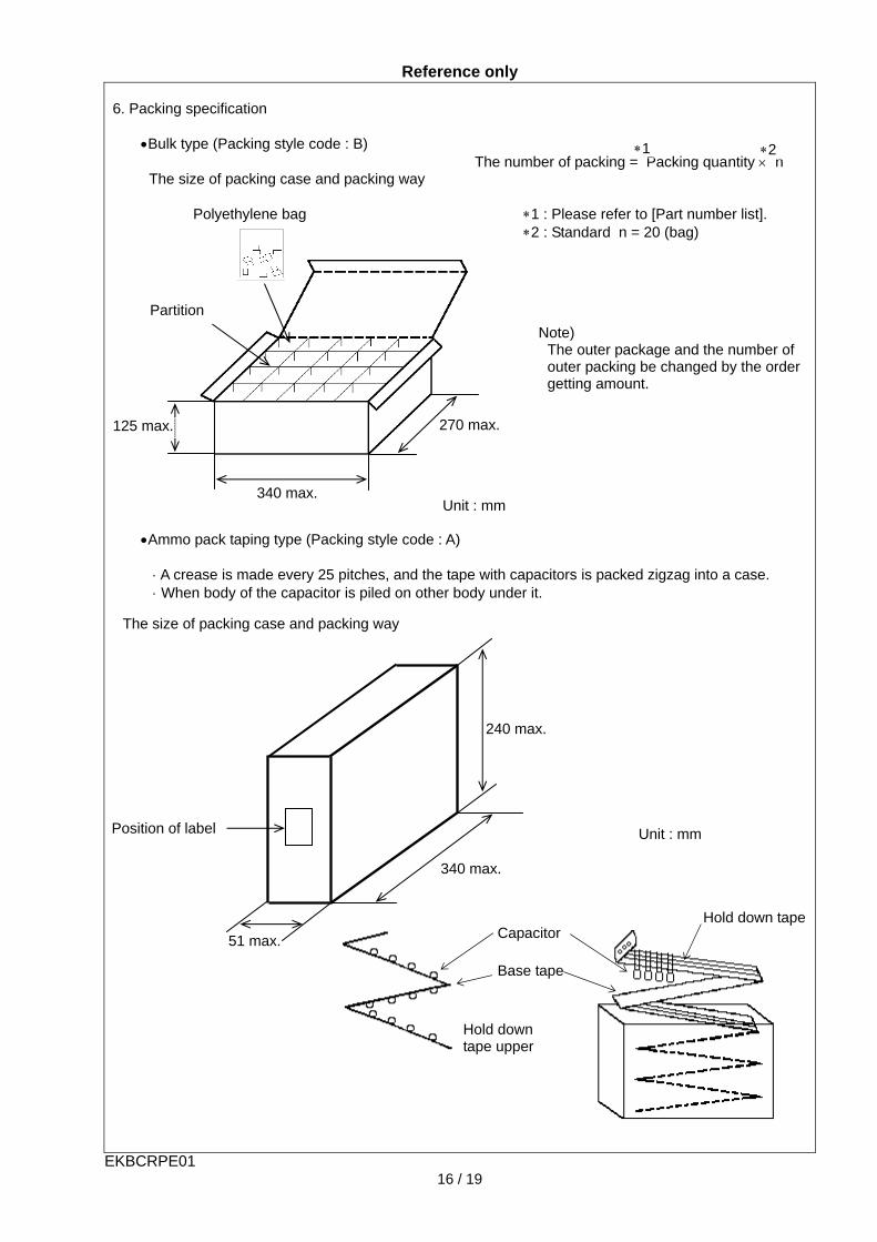
6. Packing specification Bulk type (Packing style code : B) The number of packing = Packing quantity n The size of packing case and packing way 1 : Please refer to [Part number list]. 2 : Standard n = 20 (bag) Ammo pack taping type (Packing style code : A) A crease is made every 25 pitches, and the tape with capacitors is packed zigzag into a case. When body of the capacitor is piled on other body under it.
1 2
240 max.
340 max.
Position of label
51 max.
The size of packing case and packing way
Unit : mm
Capacitor
Base tape
Hold down tape
Hold downtape upper
Unit : mm 340 max.
125 max. 270 max.
Partition
Polyethylene bag
Note) The outer package and the number of outer packing be changed by the order getting amount.

Reference only
ETP1M101 17 / 19
7. Taping specification 7-1. Dimension of capacitors on tape Inside crimp taping type < Lead code : M1 > Pitch of component 12.7mm / Lead spacing 5.0mm
Unit : mm
Item Code Dimensions Remarks
Pitch of component P 12.7+/-1.0
Pitch of sprocket hole P0 12.7+/-0.2
Lead spacing F 5.0+0.6/-0.2
Length from hole center to component center P2 6.35+/-1.3 Deviation of progress direction
Length from hole center to lead P1 3.85+/-0.7
Deviation along tape, left or right defect S 0+/-2.0 They include deviation by lead bend .
Carrier tape width W 18.0+/-0.5
Position of sprocket hole W1 9.0+0/-0.5 Deviation of tape width direction
Lead distance between reference and bottom
plane H0 16.0+/-0.5
Protrusion length 0.5 max.
Diameter of sprocket hole D0 4.0+/-0.1
Lead diameter d 0.50+/-0.05
Total tape thickness t1 0.6+/-0.3 They include hold down tape thickness.
Total thickness of tape and lead wire t2 1.5 max.
Deviation across tape h1 2.0 max.(Dimension code:W)
1.0 max.(except as above) h2
Portion to cut in case of defect L 11.0+0/-1.0
Hold down tape width W0 9.5 min.
Hold down tape position W2 1.5+/-1.5
Coating extension on lead e Up to the end of crimp
P2 P
P1
P0
L D0
H0
W0 W
1
W
0
h1 h2 S
t1 t2
Marking
W2 F
e
d

Reference only
ETP1DB02 18 / 19
Straight taping type < Lead code : DB > Pitch of component 12.7mm / Lead spacing 2.5mm
Unit : mm
Item Code Dimensions Remarks
Pitch of component P 12.7+/-1.0
Pitch of sprocket hole P0 12.7+/-0.2
Lead spacing F 2.5+0.4/-0.2
Length from hole center to component center P2 6.35+/-1.3 Deviation of progress direction
Length from hole center to lead P1 5.1+/-0.7
Deviation along tape, left or right defect S 0+/-2.0 They include deviation by lead bend .
Carrier tape width W 18.0+/-0.5
Position of sprocket hole W1 9.0+0/-0.5 Deviation of tape width direction Lead distance between reference and bottom plane H 16.0+/-0.5
Protrusion length 0.5 max.
Diameter of sprocket hole D0 4.0+/-0.1
Lead diameter d 0.50+/-0.05
Total tape thickness t1 0.6+/-0.3 They include hold down tape thickness.
Total thickness of tape and lead wire t2 1.5 max.
Deviation across tape h1
1.0 max. h2
Portion to cut in case of defect L 11.0+0/-1.0
Hold down tape width W0 9.5 min.
Hold down tape position W2 1.5+/-1.5
Coating extension on lead e 1.5 max.
P2 P
P1
P0
L D0
H
W0 W
1
W
0 h1 h2 S
t1 t2
Marking
W2 F e
d

Reference only
ETP2R01 19 / 19
7-2. Splicing way of tape
1) Adhesive force of tape is over 3N at test condition as below.
2) Splicing of tape a) When base tape is spliced
Base tape shall be spliced by cellophane tape. (Total tape thickness shall be less than 1.05mm.)
b) When hold down tape is spliced Hold down tape shall be spliced with overlapping. (Total tape thickness shall be less than 1.05mm.)
ape are spliced Base tape and adhesive tape shall be spliced with splicing tape.
c) When both tape are spliced Base tape and hold down tape shall be spliced with splicing tape.
Hold down tape
Base tape
W
Unit : mm
Progress direction in production line Hold down tape
Base tape
Cellophane tapeAbout 30 to 50
Progress direction in production line
Hold down tape
Base tape
20 to 30
Unit : mm
No lifting for the direction of progressing

Appendix
EU RoHS and Halogen Free
This products of the following crresponds to EU RoHS and Halogen Free
(1) RoHS
EU RoHs 2011/65/EC compliance
maximum concentration values tolerated by weight in homogeneous materials ・1000 ppm maximum Lead ・1000 ppm maximum Mercury ・100 ppm maximum Cadmium ・1000 ppm maximum Hexavalent chromium ・1000 ppm maximum Polybrominated biphenyls (PBB) ・1000 ppm maximum Polybrominated diphenyl ethers (PBDE)
(2) Halogen-Free
The International Electrochemical Commission’s (IEC) Definition of Halogen-Free (IEC 61249-2-21) compliance ・900 ppm maximum chlorine ・900 ppm maximum bromine ・1500 ppm maximum total chlorine and bromine
Related Documents