University of Wollongong Research Online University of Wollongong esis Collection University of Wollongong esis Collections 2013 Lead-free piezoelectric materials Abolfazl Jalalian University of Wollongong Research Online is the open access institutional repository for the University of Wollongong. For further information contact the UOW Library: [email protected] Recommended Citation Jalalian, Abolfazl, Lead-free piezoelectric materials, Doctor of Philosophy thesis, Institute for Superconducting and Electronic Materials, University of Wollongong, 2013. hp://ro.uow.edu.au/theses/4037

Welcome message from author
This document is posted to help you gain knowledge. Please leave a comment to let me know what you think about it! Share it to your friends and learn new things together.
Transcript

University of WollongongResearch Online
University of Wollongong Thesis Collection University of Wollongong Thesis Collections
2013
Lead-free piezoelectric materialsAbolfazl JalalianUniversity of Wollongong
Research Online is the open access institutional repository for theUniversity of Wollongong. For further information contact the UOWLibrary: [email protected]
Recommended CitationJalalian, Abolfazl, Lead-free piezoelectric materials, Doctor of Philosophy thesis, Institute for Superconducting and ElectronicMaterials, University of Wollongong, 2013. http://ro.uow.edu.au/theses/4037


Department of
Institute for Superconducting and Electronic Materials
Lead-Free Piezoelectric Materials
ABOLFAZL JALALIAN
"This thesis is presented as part of the requirements for the award of the Degree of Doctor of Philosophy
of the University of Wollongong"
Sep. / 2013

i
DECLARATION
I, Abolfazl Jalalian, declare that this thesis, submitted in partial fulfilment of the
requirements for the award of Doctor of Philosophy, in the Institute for
Superconducting & Electronic Materials, University of Wollongong, is entirely my
own work unless otherwise referenced or acknowledged. The document has not been
submitted for qualifications at any other academic institution.
Abolfazl Jalalian
September, 2013

ii
ABSTRACT
Quasi-one-dimensional (1D) materials, including nanofibers, nanotubes, nanowires,
and nanobelts, have been exploited widely in nanogenerators, sensors, transducers,
microelectromechanical systems (MEMS) devices, and other applications, such as
microwave varactors and ferroelectric field effect transistors. Currently available
nanostructured piezoelectric materials show a low piezoelectric coefficient d33 of
merely 100 pm V-1, with Pb(Zr, Ti)O3 (PZT)-based materials at the high end. The
health impact of lead poisoning is well known, however, and intensive efforts have
begun to discover new lead-free piezoelectric compounds which possess comparable
piezoelectric performances to those of the lead-based piezoelectric materials.
Recently, a lead-free (1-x)Ba(Ti0.80Zr0.20)O3-x(Ba0.70Ca0.30)TiO3 ((1-x)BTZ-xBCT)
piezoelectric system with optimal composition of x = 0.5 was reported to show
superior room temperature piezoelectricity, with the piezoelectric coefficient d33 =
620 pC N-1, the piezoelectric voltage constant g33 = 15.38 × 10⁻³ Vm N-1, and the
electromechanical (converse piezoelectric) response as high as 1140 pm V-1. These
superior piezoelectric properties are comparable to or higher than those of state-of-
the-art PZT or other lead-free piezoelectric compounds, due to the low polarization
anisotropy and low energy barrier for lattice distortions in the morphotropic phase
boundary (MPB) region.
The main work presented in this dissertation is focused on the synthesis and
characterization of Ba (Ti0.80Zr0.20) O3-(Ba0.70Ca0.30) TiO3 (BTZ-BCT) in different
forms including ceramics, thin films, and nanofibers.
Different structural analysis techniques, including X-ray diffraction (XRD), Raman
spectroscopy, and transmission electron microscopy (TEM), have been employed to
aj393
Highlight
aj393
Highlight

iii
investigate the evolution of the crystal structure and phase content in the samples.
The coexistence of two ferroelectric phases, tetragonal and rhombohedral, and
crystallization of the ceramics, the fibers, and the thin films in the vicinity of the
MPB region have been demonstrated. The lattice constants have been defined using
the Rietveld method. The impact of lattice parameter variations on the ferroelectric
properties of the (1-x)BTZ-xBCT ceramics has been investigated.
Different scanning probe microscopy techniques, including piezoresponse force
microscopy (PFM), scanning capacitance microscopy (SCM), and scanning
spreading resistance microscopy (SSRM), have been employed to study the
piezoelectric, ferroelectric domain switching, and the electrical properties of the
nanofibers and thin films. Very large piezoelectricity in low-dimensional BTZ-BCT
sintered as thin films (d33 = 141 pm V-1) and nanofibers (d33 = 180 pm V-1) has been
achieved. These values are comparable to those of PZT films and nanofibers.
Observations of ferroelectric nanodomains with high spatial resolution using SCM
and PFM techniques are also presented. The influences of lateral size, geometry, and
the clamping effect on the piezoelectric performance are investigated for both the
thin films and the nanofibers. The current distribution and resistivity have been
studied by SSRM. The results show a uniform distribution of resistance and very
high resistance of 1010 ohms in the BTZ-BCT nanofibers. Combining a high
piezoelectric coefficient with environmental benefits, the BTZ-BCT nanostructures
provide the superior functions that are in demand for highly efficient piezoelectric
devices and electromechanical systems.
In the last chapter of the thesis, the synthesis and characterization of biocompatible
and piezoelectric (Na,K)NbO3 (NKN) nanofibers are presented. The X-ray
diffraction pattern of the nanofibers reveals a pure single phase with polar structure
aj393
Highlight
aj393
Highlight
aj393
Highlight
aj393
Highlight

iv
after annealing at 700°C. TEM images and electron diffraction patterns show the
growth of NKN single crystals in the form of nanofibers. The ferroelectric domain
switching and piezoelectric response of the nanofibers have been investigated using
PFM. A higher piezoelectric response is achieved in NKN nanofibers (d33 = 58 pm
V-1) than in its thin films (d33 = 40 pm V-1). Owing to the existence of permanently
charged regions in the NKN nanofibers known as ferroelectric domains, electrical
signals can be generated in them via the piezoelectric effect to provide a new
opportunity for construction of a smart biocompatible scaffold that can be used for
repair, engineering, and regeneration of damaged tissues.

v
ACKNOWLEDGEMENTS
Firstly, I would like to express my sincere gratitude to my supervisor, Prof. S.X.
Dou, and my co-supervisor, Prof. X.L. Wang, for their continuous academic
guidance and support during my PhD study at the Institute for Superconducting and
Electronic Materials (ISEM), University of Wollongong.
It is my pleasure to pay tribute to Prof. A.M. Grishin, head of the Department of
Condensed Matter Physics, at the Royal Institute of Technology (KTH), Sweden, for
giving me the opportunity to work in his laboratory as a visiting PhD student and
providing me with the opportunity to attend very worthwhile courses and workshops
in scanning probe microscopy techniques. Furthermore, I would also like to thank
Dr. S. Khartsev for his technical assistance and Prof. A. Hallen and Dr. A. Srinivasan
for the use of an atomic force microscope with a scanning capacitance module.
I acknowledge Dr. Tania Silver for her help in proofreading and correction the
English in the thesis and Dr. Z.X. Cheng for his review and comments on my thesis.
I am grateful to Dr. D. Wexler, Mr. D. Attard, and Dr. M. Higgins for their
invaluable guidance and training courses in microscopy techniques in ISEM. I am
also thankful to the administrative assistants, Ms. Roberta Lynch and Mrs. Crystal
Mahfouz. I thank all my friends for the memorable times that we had together.
I would especially like to convey my gratitude to my fiancée, Ms. Nioosha Nasseh,
and all my family for their warmth, enthusiasm, love, and boundless moral support
over my entire PhD journey. Their support and care helped me to stay focused on my
work.
Finally, I would like to acknowledge the Australian Research Council (ARC) for
Discovery grant DP0879070, and the University of Wollongong and ISEM for

vi
providing me with a Matching Scholarship and International Postgraduate Tuition
Award during my PhD study.

vii
TABLE OF CONTENTS
ABSTRACT ……………………………………………………………………………... ii ACKNOWLEDGEMENTS ………………………………………………………...…... v TABLE OF CONTENTS ………………………………………………..............……... vii LIST OF FIGURES ..…………...………………………………………………….….... x LIST OF TABLES …………………………………………………………..………….. vii
Chapter 1. Literature Review ………………..…………………………………........... 1
1.1 Piezoelectricity ………………….……………………………………..... 1
1.1.1 Pyroelec.ricity ………………………………………………....... 4
1.1.2 Ferroelectricity ………………………………………………...... 7
1.1.3 Other important piezoelectric parameters …………………….... 7
1.2 Lead-based piezoelectric materials …………………………………....... 9
1.2.1 Lead titanate (PbTiO3) ………………………………………..... 9
1.2.2 Lead zirconate titanate ( Pb(Zr, Ti)O3) ………………………..... 10
1.2.3 Other lead-based materials …………………………………….... 12
1.2.4 Environmental issues ………………………………………….... 12
1.3 Lead-free piezoelectric materials ……………………………..………..... 12
1.3.1 Bismuth based layered perovskite structures ……….…………... 13
1.3.2 Potassium sodium niobates ………………………….………...... 15
1.3.3 Barium titanates …………………………………….………….... 16
1.3.4 Other lead-free piezoelectric materials ……..…………………... 22
1.4 Low-dimensional piezoelectric properties measurements ………............. 23
1.5 Research motivation …………………………………………………....... 25
viii
1.6 References…………………………………………………………….... 28
Chapter 2. BTZ-BCT Ceramics ……………………………………………….…...... 35
2.1 Introduction ………………………………………..………………...... 35
2.2 Experimental procedure ……………………………..……………....... 36
2.3 Results and discussions …………………….………………………..... 36
2.3.1 Crystalline structure and vibration modes …………………...... 36
2.3.2 Ferroelectric and piezoelectric properties ……………………... 42
2.4 Conclusions ………………………………………………………......... 46
2.5 References ……………………………………………………………... 47
Chapter 3. BTZ- BCT Nanofibers ………………………………………..................... 49
3.1 Introduction …………………………………………………………..... 49
3.2 Experimental procedure ………………………………………….......... 50
3.3 Results and discussion …………………………………………............ 52
3.3.1 Microstructure and crystalline phase evolution ……………...... 52
3.3.2 Vibration modes ……………………………………………….. 56
3.3.3 Crystalline phase observations by TEM ……………………...... 58
3.3.4 Piezoelectric and ferroelectric measurements by PFM ……….... 59
3.3.5 Ferroelectric nanodomain imaging by SCM ………………….... 65
3.3.6 Electric resistance measurements by SSRM ………………….... 67
3.4 Conclusions ……………………………………………………..................... 69
3.5 References …………………………………………………………….. 70
aj393
Highlight
aj393
Highlight

ix
Chapter 4. BTZ -BCT Thin Films ……………………………………….................... 74
4.1 Introduction ………………………………………………………........ 74
4.2 Experimental procedure …………………………………................. 75
4.3 Results and discussion ……………………………………………....... 76
4.3.1 Morphology studies using FE-SEM and AFM ……………...... 76
4.3.2 Phase content investigation using XRD and Raman spectroscopy 77
4.3.3 Piezoelectric and ferroelectric properties investigation by PFM 78
4.4 Conclusions ………………………………………………………........ 84
4.5 References ……………….………………………………………......... 84
Chapter 5. Biocompatible Piezoelectric Nanofibers …………………………........... 87
5.1 Introduction ………………………………………………………........ 87
5.2 Experimental procedure ……………………………………………..... 89
5.3 Results and discussions ……………………………………………..... 90
5.3.1 Morphology and Crystalline phase evolution ………………... 90
5.3.2 Nanostructure studies by TEM ……………………...………... 94
5.3.3 Piezoelectric and ferroelectric properties ………………..….... 95
5.4 Conclusions …………………………………………………...…….... 99
5.5 References ………………………………………………………...….. 100
CONCLUSIONS RECOMMENDATIONS..................................................................... 103
PUBLICATIONS ……………………………………………………………………... 107
aj393
Highlight

x
LIST OF FIGURES
Figure 1.1 Symmetry hierarchy for piezoelectricity according to the
crystallographic point groups.
2
Figure 1.2 Schematic representation of the direct piezoelectric effect. 3
Figure 1.3 Schematic representation of the inverse piezoelectric effect. 3
Figure 1.4 Directions in a piezoelectric unit cell according to the Cartesian
coordinates system.
4
Figure 1.5 (a) Hexagonal structure of β-quartz and its coordination vectors. (b)
Schematic illustration of the piezoelectric phenomenon in quartz as
a non-polar piezoelectric material.
6
Figure 1.6 Phase diagram of lead zirconate titanate. 10
Figure 1.7 Schematic illustration of possible domain orientations in (a)
tetragonal structure: 6 directions and (b) rhombohedral structure: 8
directions.
11
Figure 1.8 Bismuth layered structure in BLSF [27]. 13
F igure 1.9 (a) Effect of Nb5+ doping on the resistivity and (b) effect of V5+ on
the dielectric permittivity of the Bi4Ti3O13 .
14
Figure 1.10 Equilibrium phase diagram of the KNbO3-NaNbO3 system. 15
Figure 1.11 (a) Barium titanate crystalline structures at different temperatures.
(b) Dielectric constant of BaTiO3 as a function of temperature.
17
Figure 1.12 (a) Tetragonal perovskite structure of BaTiO3. (b) Piezoelectric
effects in a BaTiO3 unit cell due to Ti displacement under an
external electric field E .
18
Figure 1.13 (a) Equilibrium phase diagram of the BaTiO3-CaTiO3 system [45]. (b)
Piezoelectric constants of <100>c oriented (Ba,Ca)TiO3 single
crystals and zone-melt biphasic polycrystals.
19
Figure 1.14 (a) Hysteresis loops of 40BCT, 40BCT,and 60BCT. (b1) Saturation
polarization, Pm, (b2) remnant polarization, Pr, (b3) coercive field,
Ec, (b4) permittivity, (b5) piezoelectric coefficient, d33, and (b6)
converse piezoelectric coefficient d = S/E. Values of various PZTs
are also shown as a reference. (c) Comparison of d33 among BZT-
50BCT and other non-Pb piezoelectrics, and yjr PZT family. (d)
20

xi
Comparison of the electrostrain versus electric field among BZT-
50BCT and various PZTs. (e1) Temperature dependence of the direct
piezoelectric coefficient in BZT-50BCT. (e2) Temperature
dependence of the direct piezoelectric coefficient in BZT-45BCT
(f) Phase diagram of pseudo-binary ferroelectric system
Ba(Zr0.20Ti0.80) O3-(Ba0.70Ca0.30)TiO3, abbreviated as BZT-BCT.
Figure 1.15 (a) Schematic illustration of the tilted MPB developed in the BZT-
xBCT system. Point b represents the TCP and c, d, and e identify
three different molar ratios x at different temperatures along the
MPB. (b),(c),(d), and (e) represent the 1D free energy barrier plot
against the polarization rotation from rhombohedral (PR) to
tetragonal (PT) and vice versa. (f) Dielectric constant vs.
temperature change in Ba(Zr0.15Ti0.85)O3 (rhombohedral phase) and
(Ba0.80Ca0.20)TiO3 (tetragonal phase) .
21
Figure 1.16 ZnO unit cell in the wurtzite structure. 22
Figure 1.17 (a) Schematic illustration of the PFM experimental set up. (b)
Surface displacement of a piezoelectric sample due to the inverse
piezoelectric effect exhibited by the ferroelectric domains under
applied electric field.
23
Figure 1.18 (a) Schematic illustration of the a-domains and c-domains in a
crystal. (b) Possible movements of the cantilever due to a force
developed by the interaction of different domains with the applied
AC signal, in which Fdefl results in deflection, Fbuck leads to buckling,
and Ftor creates torsion in the cantilever. (c) Side- and top-view of
the cantilever movement. (d) Possible movements of the laser spot
on the photodetector. Fdefl and Fbuck result in a vertical signal, while
only Ftor results in a lateral signal.
25
Figure 2.1 XRD patterns (left) of the (1-x)BTZ-xBCT ceramics sintered at
1450°C for 2 h in air and enlarged peaks located at 2θ ≈ 31.5º fitted
by the Lorentzian function for different x values. Coexistence of two
polar phases, both tetragonal (T) and rhombohedral (R), confirms
the crystallization of BTZ-BCT ceramics in yjr vicinity of the MPB
region. The peak shifts observed in different samples can be
37
aj393
Highlight
aj393
Highlight
aj393
Highlight
aj393
Highlight

xii
attributed to the internal strain developed by the substitution of Ca2+
in the Ba+2 sites and Ti+4 in the Zr4+ sites in the BTZ ceramics.
Figure 2.2 Refinement patterns of the (a) BTZ, (b) 0.9BTZ-0.1BCT, (c)
0.8BTZ-0.2BCT, (d) 0.7BTZ-0.3BCT, and (e) 0.6BTZ-0.4BCT
ceramics sintered at 1450°C for 2 h in air. The symbols mark the
experimental results for the XRD pattern that is fitted in red. The
short blue vertical lines mark the line positions of the standard, and
the green spectrum at the bottom is the difference spectrum between
the fit and the experimental results.
38
Figure 2.3 (a) FE-SEM image of the particle size distribution and morphology
of the grains in the BTZ-BCT ceramic sintered at 1450°C for 2 h in
the air. (b) Higher magnification image of the area indicated by the
square in (a) that shows the growth steps in individual grains.
41
Figure 2.4 Different vibration modes in the (1-x)BTZ-xBCT system were
investigated by Raman spectroscopy at room temperature.
41
Figure 2.5 Typical polarization versus electric field hysteresis loop (P-E loop)
in a ferroelectric material.
43
Figure 2.6 (a) Maximum polarization Ps is increased by introducing BCT into
the BTZ structure, and the maximum Ps= 13.32 μC cm-2 at x = 0.5 in
the (1-x)BTZ-xBCT system. (b) Correlation of the polarization
saturation enhancement with the decrease in the unit cell volume in
the (1-x)BTZ-xBCT ceramics. (c) The BTZ-BCT ceramic achieved
the maximum spontaneous polarization Ps = 13.86 μC cm-2 under
an electric field E = 40 kV cm-1 at room temperature. (d)
Piezoelectric response enhancement in the BTZ-BCT ceramic
compared to other compositions in this system.
45
Figure 3.1 FE-SEM images of the BTZ-BCT nanofibers (a) calcined at 500°C,
(b) at 600°C (c) at 700°C. And (d) at 800°C for 1 hour. Insets:
highly magnified views of annealed BTZ-BCT nanofibers. All
images were collected under 0.5 kV acceleration voltage and 3.7
mm working distance without conductive coating.
53
Figure 3.2 Energy dispersive X-ray spectroscopy (EDS) of the BTZ-BCT
nanofibres annealed at 700°C. The inset table shows the
54
aj393
Highlight
aj393
Highlight
aj393
Highlight
aj393
Highlight
aj393
Highlight
aj393
Highlight
aj393
Highlight
aj393
Highlight
aj393
Highlight
aj393
Highlight
aj393
Highlight

xiii
concentrations of the different elements.
Figure 3.3 (a) XRD patterns of the BTZ-BCT nanofibers annealed at different
temperatures with corresponding Miller indices of BaTiO3.
Enlarged scans of Bragg diffraction reflections (b) for {110} at 2θ =
31.7 ° and (c) {200} at 2θ = 45.5 ° for the BTZ-BCT nanofibers
annealed at 700 °C. The peaks are fitted by Lorentzian functions.
Coexistence of rhombohedral and tetragonal phases proves that
crystallization of the nanofibers has occurred in the vicinity of the
morphotropic phase boundary.
55
Figure 3.4 Raman scattering spectra of the BTZ-BCT nanofibers annealed at
500, 600, 700, and 800 °C for 1 hour in air. Since the [A1(TO)] peak
at 164 cm-1 exists only in the rhombohedral phase of BaTiO3
nanocrystals, it indicates the coexistence of rhombohedral (R) and
tetragonal (T) phases in the MPB region at temperatures above
700°C.
56
Figure 3.5 TEM results obtained from sample heat-treated at 700° C: (a) low
magnification image of a nanofibre containing larger tetragonal and
smaller rhombohedral particles, with inset selected area electron
diffraction pattern; (b) indexing of the regions indicated in red and
green in (a) of {110} group reflections according to the indicated
rhombohedral (R) and tetragonal (T) phase reflections; (c) a second
selected area diffraction pattern with rhombohedral and tetragonal
reflections as indicated; (d) high magnification image with region
containing fine twins indicated.
58
Figure 3.6 . Force-distance curve recorded from the surface of a silicon
substrate using the cantilever employed in our PFM measurements.
This plot was used for the optical sensitivity calibration of the
cantilever.
60
Figure 3.7 (a) Local PFM phase hysteresis loops and (b) piezoelectric butterfly
loops of the BTZ-BCT nanofiber obtained by switching the dc-bias
voltage from -5 to +5 volts. 180° domain switching in the phase
hysteresis loop shows the switching of spontaneous electrical
61
aj393
Highlight
aj393
Highlight

xiv
dipoles built up in the BTZ-BCT fiber. (c) d33 hysteresis loop
calculated by using the converse piezoelectric equation, Δz = d33V,
which indicates a significant enhancement of d33 = 180 pmV-1 in the
BTZ-BCT nanofiber. (d) 3D topographic atomic force microscope
(AFM) image of the nanofiber used for the PFM measurements.
Figure 3.8 Comparison of piezoelectric coefficient d33 in nanostructured
components used to build piezoelectric generators with d33 in our
BTZ-BCT films and fibers.
63
Figure 3.9 (a) Topographical (AFM), (b) SCM images, obtained in contact
mode, of a single BTZ-BCT nanofiber annealed at 700°C on a
Si/SiO2/Ti/Ir conductive substrate. The two distinct types of regions
in black and white represent opposite out-of-plane electric domains,
averaging 24 nm in size and (c) schematic illustration of the SCM
measurement. The sign and magnitude of the C-V slope in the SCM
image is recorded while the AC bias is applied to a local capacitor
constructed by the nanofiber and conductive tip, and the substrate as
top and bottom electrodes, respectively. The ferroelectric domain
polarities and their configurations are developed in the dC/dV image
in the SCM as a result of different trends in the dC/dV with respect
to the polarization states.
66
Figure 3.10 (a) Topographical (AFM), (b) SSRM images, obtained in contact
mode, of a single BTZ-BCT nanofiber annealed at 700°C on a
Si/SiO2/Ti/Ir conductive substrate. The two distinct types of regions
in dark and bright colours represent the current distribution in the
conducting substrate and ferroelectric nanofiber. (c) Section analysis
of the SSRM image, and (d) reference transfer curve of the SSRM
logarithmic current amplifier in different biases.
68
Figure 4.1 (a) FE-SEM image of BTZ-BCT thin film deposited on the
Si/SiO2/Ti/Ir substrate and annealed at 700°C for 1 hour in air. Inset:
magnified view of the thin film surface. (b) FE-SEM image of cross-
section of BTZ-BCT thin film about 200 nm in thickness with an
average particle size of 33 nm. (c) 3D AFM image of topography of
BTZ-BCT thin film annealed at 700°C for 1 hour, showing 2 nm
76
aj393
Highlight
xv
rms surface roughness.
Figure 4.2 (a) X-ray diffraction pattern of the BTZ-BCT thin film annealed at
700°C on the Si substrate. (b) Raman spectrum of BTZ-BCT 200
nm thick BTZ-BCT film spin-coated on Si/SiO2/Ti/Ir substrate
annealed at 700°C for 1 hour in air. The spectrum of the substrate
alone is included for reference. All features are characteristic of the
polar structure of BaTiO3 and indicate successful evolution of the
perovskite structure in all samples. The existence of a peak at 164
cm-1 [A1(TO)] is only observed in the rhombohedral symmetry,
while the other peaks, which appear in both tetragonal and
rhombohedral symmetries, indicate the crystallization in
morphotropic phase boundary (MPB) region.
78
Figure 4.3 3D PFM phase (a) and amplitude (b) images of the surface of 200
nm thick BTZ-BCT film. Ferroelectric domain patterns in the phase
image (a) display the opposite polarity of ferroelectric domains 20 to
40 nm in size. These domains are revealed by 180° phase difference
contrast. The amplitude image (b) reproduces the domain shape.
Sharp contrast around domains visualizes domain boundaries. In (c),
phase and amplitude profiles recorded along the marked lines in (a)
and (b) are overlaid on an AFM topographical image. All three
images were collected simultaneously under 1.0 V ac modulation
voltage.
79
Figure 4.4 (a) Local PFM phase hysteresis loops and (b) piezoelectric
butterfly loops of the BTZ-BCT thin film obtained by switching the
bias voltage from -5 to +5 volts (±300 kV cm-1 electric field). 180°
domain switching in the phase hysteresis loop shows the switching
phenomenon of spontaneous electrical dipoles built up in the BTZ-
BCT thin film. (c) d33 hysteresis loop calculated by using the
converse piezoelectric equation, Δz = d33V, which indicates the
piezoelectric coefficient d33 = 141 pmV-1 in the BTZ-BCT thin film.
(d) Schematic illustration of lateral size and contact area in the thin
film and nanofiber.
80
Figure 4.5 Polarization versus electric field (P-E) loop obtained at 1 kHz of the 83
aj393
Highlight
aj393
Highlight
aj393
Highlight

xvi
BTZ-BCT thin film with about 200 nm thickness deposited on the
Si/SiO2/Ti/Ir substrate.
Figure 5. 1 FE-SEM images of (Na,K)NbO3 nanofibers mat (a) annealed at 600
°C, (b) 700 °C and (c) 800 °C in air. (d) Thermogravimetric analysis
of NKN nanofibers from room temperature up to 800 °C in air. 62
wt% of the NKN precursor evaporates or burns out during the
annealing process at different stages.
90
Figure 5.2 Energy dispersive x-ray spectroscopy (EDS) spectrum of the NKN
nanofibers annealed at 800°C. Inset: quantitative analysis of the
EDS that approves the existence of the constructive elements in the
(Na, K) NbO3 nanofibers which follow the stoichiometric ratios with
reasonable accuracy.
91
Figure 5.3 XRD patterns of the (Na, K) NbO3 nanofibers annealed at 700 and
800°C reveal the crystallization of the nanofibers in a monoclinic
structure. All peaks are indexed according to the PDF-card number
77-0038 corresponds to the (Na0.35K0.65) NbO3.
92
Figure 5.4 Experimental Raman spectrum of the NKN-nanofibers annealed at
800 °C for 1 hour in air.
93
Figure 5.5 TEM results obtained from sample heat treated at 800° C; (a) low
magnification image of a nanofiber containing single crystals. (b)
Selected area electron diffraction pattern which reveals the single
crystal. (c) High resolution TEM image of the NKN nanofiber. (d)
Schematic of a monoclinic structure.
95
Figure 5.6 3D-PFM (a) topography, (b) phase and (c) amplitude images of the
NKN nanofiber. Ferroelectric domain pattern in the phase image (b)
displays the opposite polarity of ferroelectric domains. These
domains are revealed by 180° phase difference contrast. The
amplitude image (c) represents the piezoelectric response of the
NKN nanofiber generated by the movement of the nanofiber under
alternate electric field developed between the tip and conducting
substrate. The PFM-phase and amplitude images are overlaid on the
topography image and collected simultaneously under 1.2 V ac
modulation voltage. (d) Displays the interaction of ferroelectric
98
aj393
Highlight

xvii
domains with essential elements for the tissue growth and
osteoconduction including fibrins and calcium ions respectively.
Figure 5.7 (a) Local PFM phase hysteresis loop and (b) piezoelectric butterfly
loop of the NKN nanofiber obtained by switching the bias voltage
from -5 to +5 volts at 25 Hz. 180° domain switching in the phase
hysteresis loop shows the switching phenomenon of spontaneous
electrical dipoles built up in the NKN nanofiber. (c) d33 hysteresis
loop calculated by using the converse piezoelectric equation, Δz =
d33V, indicates a significant enhancement of d33 = 58 pmV-1 in the
NKN nanofiber. (d) 3D topographical image of the NKN nanofiber
with 200 nm width and 100 nm height, used in PFM measurements.
99

xviii
LIST OF TABLES
Table 1.1 Centrosymmetric and non-centrosymmetric point groups in crystals. 5
Table 1.2 Comparison of piezoelectric properties in different BLSF
compositions.
14
Table 1.3 Piezoelectric coefficients of ZnO, AlN, and GaN in the forms of thin
films and single crystal.
22
Table 2.1 Lattice parameters and unit cell volumes of the (1-x)BTZ-xBCT
ceramics extracted from the Rietveld refinement results on the
ceramics.
40
Table 3.1 Comparison of the piezoelectric coefficient d33 of the BTZ-BCT
nanofibres with lead-based and lead-free piezoelectric nanofibres.
62
Table 3.2 Calculated effective stress induced by electric field in the nanofiber-
substrate interface.
65
Table 4.1 Comparison of the piezoelectric coefficient d33 in some Pb-based and
Pb-free piezoelectric thin films.
81
Table 4.2 Calculated effective stress induced by electric field in the thin film −
substrate interface.
82
aj393
Highlight
aj393
Highlight

xix

1
Chapter 1. Literature Review
1.1 Piezoelectricity
Piezoelectricity was discovered by the Curie brothers, Jacques and Pierre Curie, in
1880[1]. They observed electrical charges generated on the surfaces of some crystals,
including quartz (SiO2), the boron silicate crystal mineral group (tourmaline), topaz
(Al2SiO4(F,OH)2), cane sugar (C12H22O11), and Rochelle salt (KNaC4H4O6·4H2O),
when an appropriate load (stress) was applied to them. The phenomenon, which
involves the generation of electricity by mechanical deformation (strain) in some
materials, was called piezoelectricity, and the behaviour was considered as a direct
piezoelectric response. In 1881, Lippmann mathematically predicted an inverse
piezoelectric phenomenon, in which an electric field leads to a mechanical
deformation. He established the fundamental thermodynamic principles to represent
the converse piezoelectricity. The Curie brothers immediately confirmed the
converse piezoelectric phenomenon experimentally in 1881.
Just after the discovery of piezoelectricity, much more work was done to define the
crystallographic principles of this effect. In 1910, the piezoelectric effect was defined
with respect to crystallographic point groups in the first textbook published on
physical crystallography by Voigt[1]. Among the 32 crystallographic point groups,
only 21 are non-centrosymmetric structures, and apart from the 432 point group, the
other 20 groups are categorized as piezoelectric materials (Figure 1.1).

2
Figure 1.1 Symmetry hierarchy for piezoelectricity according to the crystallographic
point groups.
In the direct piezoelectric effect, the generated charge Q is proportional to the
applied force. The charge density D (dielectric displacement) is calculated using
Equation (1.1):
𝐷 = 𝑑𝑇 (1.1)
Where d is the piezoelectric coefficient in coulombs/Newton (C/N) and T in
Newtons/unit area is the applied stress. Changing from a compressive to a tensile
stress or vice versa reverses the sign of the direct piezoelectric coefficient. Figure
(1.2) shows the direct piezoelectric effect schematically in a piezoelectric material.

3
Figure 1.2 Schematic representation of the direct piezoelectric effect.
In the inverse piezoelectric effect, the induced strain S is proportional to the applied
electric field E
𝑆 = 𝑑𝐸 (1.2)
Where the inverse piezoelectric coefficient is expressed by d with units of meter/volt.
When the strain changes from a contraction to an expansion or vice versa, the sign
changes for the converse piezoelectric coefficient. The inverse piezoelectric
phenomenon is illustrated in Figure 1.3.
Figure 1.3 Schematic representation of the inverse piezoelectric effect.
Since the piezoelectric response is an anisotropic phenomenon, the piezoelectric
constant and other related parameters are represented by ij indices such as dij, in
which i denotes the direction of the polarization or electrical input/output and j

4
represents the direction of the strain or mechanical deformation developed or
applied. The subscripts are defined in a Cartesian coordinates system including X, Y,
and Z (Figure 1.4). The numbers 1-3 are assigned to the longitudinal parameters and
4-6 represent the shear mode.
Figure 1.4 Directions in a piezoelectric unit cell according to the Cartesian
coordinates system.
For example, the d31 mode identifies a mechanical deformation (strain) along the 1
(X) axis when an electric field is applied along the 3 (Z) axis, and d33 describes the
generated charge (electric field) along the 3 (Z) direction while a mechanical stress is
applied along the same direction as the electric field in the direct piezoelectric
phenomenon and vice versa in the inverse piezoelectric response.
1.1.1 Pyroelectricity
A subgroup of the piezoelectric materials consisting of 10 point groups possesses a
unique polar axis in a certain crystal direction due to an existing electric dipole. The
dipole moment can be changed by exposing these materials to uniform heat that leads
to a surface electric charge. Changing the magnitude of the dipole with temperature

5
is demonstrated in this subgroup of the piezoelectric materials as the pyroelectricity.
An electric dipole is constructed by separation of positive and negative charges in a
unit cell. Pyroelectric materials possess a spontaneous polarization, PS, which cannot
be reoriented by an external electric field. When these materials are heated,
increasing the temperature leads to a change in the spontaneous polarization and can
be detected according to Equation (1.3)
𝑑𝑃𝑠 = −𝑝 𝑑𝑇 (1.3)
Where 𝑑𝑃𝑠 is the polarization change created by the 𝑑𝑇 temperature variation. The
pyroelectric effect is defined by 𝑝 . The polarization is suppressed in the pyroelectric
materials when the temperature increases, and it is represented by the negative sign
in Equation 1.3.
Table 1.1 Centrosymmetric and non-centrosymmetric point groups in crystals [2].
Crystal
structure Point group
Centro-
symmetric
Non-centrosymmetric (Piezoelectric)
Non-polar Polar
Triclinic 1�, 1 1� ― 1
Monoclinic 2, m, 2/m 2/m ― 2,m
Orthorhombic 222, mm2, mmm mmm 222 mm2
Tetragonal 4, 4/m, 422, 4mm, 4�,
4/mmm, 4�2m or 4�m2 4/m, 4/mmm
422, 4�, 4�2m
or 4�m2
4,
4mm
Rhombohedral 3, 3�, 32, 3m, 3�m 3�m, 3� 32 3,3m
Hexagonal 6, 6/m, 622, 6mm, 6/mmm,
6�, 6�m2 or 6�2m 6/m, 6/mmm
622, 6�, 6�m2
or 6�2m
6,
6mm
Cubic 23, m3, 432, m3m, 4�3m m3, m3m 23, 432, 4�3m ―

6
In piezoelectric crystals apart from the pyroelectrics, dipoles are arranged in
compensating directions in such a way that the net crystal dipole moment is zero.
These crystals are polarized when the load (stress) is applied, and a net crystal dipole
is developed in a favoured direction. Crystallographic point groups in polar and non-
polar piezoelectric materials are represented in Table 1.1. Quartz is a well know non-
polar piezoelectric material. Figure 1.5 demonstrates the piezoelectric response
mechanism in quartz crystal.
Figure 1.5 (a) Hexagonal structure of β-quartz and its coordination vectors. (b)
Schematic illustration of the piezoelectric phenomenon in quartz as a non-polar
piezoelectric material.
The favoured direction for the polarization in quartz is along the a-axis in its unit
cell. Regarding the hexagonal structure in the β-quartz, there are three polarization
directions separated by 120° from each other (Figure 1.5(a)). It should be noted that
in a non-polar crystal, when a uniform hydrostatic pressure is applied to the crystal,
the net polarization is zero and only by applying the pressure in an individual
polarization direction, is a non-zero net polarization developed (Figure 1.5(b)).
(a) (b)

7
1.1.2 Ferroelectricity
Ferroelectric materials are a subclass of the pyroelectrics and consequently, the
piezoelectric materials. The spontaneous polarization in ferroelectrics is reversible
and switchable under an alternated electric field, whereas in the non-ferroelectric
pyroelectric materials, it remains unchanged when an external electric field is
applied. In the other words, there must be more than one equilibrium state for the
spontaneous polarization in ferroelectrics, so that the polarization vector can be
switched between those states. In the non-ferroelectric pyroelectric materials,
however, there is only one possible state. It should be noted, as is demonstrated in
Figure 1.1, that all ferroelectric materials are pyroelectric and consequently
piezoelectric, but all pyroelectric and piezoelectric materials are not ferroelectric.
1.1.3 Other important piezoelectric parameters
Piezoelectric voltage constant
The piezoelectric voltage constant, g, is defined as the electric field developed by a
stress in a piezoelectric material in units of mV N-1 that can be calculated using
Equations (1.4) and (1.5)
𝑔33 = 𝑑33𝜀0𝐾3𝑇
(1.4)
Where K is the relative dielectric constant and
𝑔31 = 𝑑31𝜀0𝐾3𝑇
(1.5)
Mechanical quality factor Qm
The mechanical quality factor, Qm, is the ratio of the stored energy to the wasted
energy in a cycle when a piezoelectric material is subjected to a periodic vibration,
and Qm-1 represents the mechanical loss[3]. It is also demonstrated that mechanical

8
strain in a piezoelectric resonant is amplified by a factor proportional to Qm at its
resonance frequency compared to the strains in off-resonance frequencies. In a
highly efficient actuator, a high Qm and low loss are essential.
The mechanical quality factor can be calculated in piezoelectric materials by using
Equation (1.6)
𝑄𝑚 = 12𝜋𝑓𝑟𝑍𝑚𝐶0
� 𝑓𝑎2
𝑓𝑎2 − 𝑓𝑟2� (1.6)
Where fr and fa are the resonance and anti-resonance frequencies. Zm is the minimum
impedance at resonance frequency and C0 represents the low frequency capacitance.
Coupling factor K
The electromechanical coupling factor, K, demonstrates the efficiency of a
piezoelectric material in the conversion of the mechanical energy into electricity and
vice versa. Three important coupling factors in piezoelectric materials are the planar
coupling coefficient Kp, the length extensional coupling coefficient K31, and the
thickness extensional coupling coefficient K33. These coefficients are calculated by
Equations (1.7)-(1.10) using the resonance and anti-resonance frequencies.
𝐾332 = 𝜋2
1+𝑓𝑎−𝑓𝑟𝑓𝑟
tan �𝜋(𝑓𝑎−𝑓𝑟)
2𝑓𝑟
1+(𝑓𝑎−𝑓𝑟)𝑓𝑟
� (1.7)
And if
𝜓 = 𝜋2�1 + 𝑓𝑎−𝑓𝑟
𝑓𝑟� tan �𝜋(𝑓𝑎−𝑓𝑟)
2𝑓𝑟� (1.8)
Then
𝐾312 = 𝜓𝜓+1
(1.9)
And
𝐾𝑝 = 𝑓𝑎2 − 𝑓𝑟2
𝑓𝑟2 (1.10)

9
1.2 Lead-based piezoelectric materials
1.2.1 Lead titanate (PbTiO3)
Lead titanate is one of the essential basic compounds used in commercially
employed piezoelectric materials, however, its pure form is not of interest to
industry. PbTiO3 is crystallized in the tetragonal structure with c/a ratio of 1.06 in the
P4mm space group at room temperature[4].
There have been few practical results on the piezoelectric and ferroelectric properties
of the PbTiO3 single crystals due to their high electrical conductivity, which could
originate from a high concentration of Pb vacancies, especially in high temperature
processes. They possess a piezoelectric constant d33 = 84-117 pC N-1 and dielectric
constant k33 = 80-126 [2, 5, 6].
In PbTiO3 ceramics, low resistivity together with the mechanical fracturing caused
by thermal expansion anisotropy and large spontaneous strain during the cubic to
tetragonal phase transition results in low dielectric and piezoelectric properties. In
modified PbTiO3 structures, however, introducing a variety of additives, mainly rare
earths ((Pb1-3/2xRex) TiO3) and alkaline elements ((Pb1-xCax)TiO3), has improved the
electrical resistivity and reduced the spontaneous strain by decreasing the Curie
temperature and tetragonality of pure PbTiO3 and made the doped compounds
appropriate dielectrics with useful electromechanical properties[7-10]. In the modified
lead titanate ceramics, the piezoelectric coefficient has been improved up to more
than 90 pC N-1 .
1.2.2 Lead zirconate titanate ( Pb(Zr,Ti)O3)
Lead zirconate titanate (PZT) is a solid solution of lead zirconate (PbZrO3) and lead
titanate (PbTiO3). PbZrO3 is an antiferroelectric. According the definition presented

10
by Kittel, in the antiferroelectric materials, spontaneous electric polarizations are
arranged in the antiparallel direction, so that the net polarization is zero and they are
not piezoelectric [11]. Interestingly, a pseudo binary system PbZrO3-x PbTiO3 (Pb(Zr1-
xTix)O3) or PZT exhibits very useful piezoelectric and ferroelectric properties. The
phase diagram of Pb(Zr1-xTix)O3 is shown in Figure 1.6. The rhombohedral region
contains two symmetries, including a low temperature rhombohedral form with R3c
symmetry and a high temperature one with R3m symmetry. As is mentioned in
Figure 1.6, the Ti-rich tetragonal region undergoes a direct phase transition from
tetragonal to cubic, however, the Zr-rich rhombohedral phase experiences a phase
change from the low temperature rhombohedral to the high temperature
rhombohedral structure before crystallizing in a cubic structure.
Figure 1.6 Phase diagram of lead zirconate titanate[12].
PZT with molar ratio x = 0.47-0.50 is crystallized in a unique region in its phase
diagram called the morphotropic phase boundary (MPB), so that two polar structures,
including the rhombohedral (R3m) and tetragonal (P4mm), can coexist.

11
Enormous attempts have been undertaken to understand the role of the MPB in the
superior piezoelectric performance of PZT, where d33=290 pC N-1, Qm=1000, Kt =
0.47, ε33=1300, and tan 𝛿 = 0.005 [12-16].
The most plausible explanation refers to the large amount of active polarization
orientation that exists in the MPB region and the flattening of the free energy profile
for switching spontaneous polarization vectors. Figure 1.7 shows 14 possible domain
orientations: 6 directions in tetragonal <001> (Figure 1.7(a)) and 8 directions in
rhombohedral <111> (Figure 1.7(b)) structures. This means there are 14 (6+8 = 14)
variants for switching of spontaneous polarization vectors in the vicinity of the MPB.
Variability of polarization switching and flattening of the free energy profile provide
efficient polarization reorientation during the poling procedure and remarkably
enhance the piezoelectric properties in the MPB region [17-20].
Figure 1.7 Schematic illustration of possible domain orientations in (a) tetragonal
structure: 6 directions and (b) rhombohedral structure: 8 directions.
PZT-based materials exhibit outstanding piezoelectric and ferroelectric properties
and have been used widely in different aspects of science and technology.

12
1.2.3 Other lead-based materials
The outstanding piezoelectric and ferroelectric properties of PZT have attracted
many attempts to investigate the other possible lead-based piezoelectric materials.
Many compositions and complex systems have been studied, and some of them have
become objects of interest because of their interesting performances. Compositions
such as Pb2Nb2O6 [21], Pb(Zn1/3Nb2/3)O3–PbTiO3(PZN–PT) [22, 23], Pb(Mg1/3,Nb1/3)O3–
PbTiO3 (PMN–PT) [24], Pb (Ni1/3Nb1/3)O3–Pb(Zr,Ti)O3 (PNN–PZT) [25], and
Pb(Sc1/2Nb1/2)O3-PbTiO3 [26] have been investigated, and the results were published.
1.2.4 Environmental issues
Lead (Pb) is one of the most toxic materials known, and continuous exposure to an
environment contaminated by this element has potential hazards. Being in contact
with Pb can cause serious damages to vital human organs such as the kidney, heart,
and brain. Since most commercial piezoelectric materials are based on PZT
containing about 60 wt% lead, intensive efforts have been undertaken to eliminate
the Pb and find good replacement candidates[27].
1.3 Lead-free piezoelectric materials
There has been a growing interest in developing alternative lead-free piezoelectric
materials that can eventually replace the current lead-based ones. Intensive research
efforts have been spent on related studies all around the world for over two decades.
In the following sections, current lead-free piezoelectric materials will be reviewed.
1.3.1 Bismuth based layered perovskite structures
Bismuth layered perovskite structure ferroelectrics (BLSF) with the chemical
formula Bi2Ax-1BxO3x+3 is another group of lead-free piezoelectric materials. This

13
structure comprises perovskite layers periodically separated by (Bi2O2)2+ layers
(Figure 1.8). As demonstrated in Figure 1.8 the layered structure in the BLSF leads
to a plate-like morphology in its microstructure [28, 29].
Figure 1.8 Bismuth layered structure in BLSF [27].
The high Curie temperatures (600°C ─ 900°C) in BLSF compositions, much higher
than those of the lead-based materials (200°C ─ 400°C), mak e the BLSF materials
good candidates as pyroelectric sensors and high temperature piezoelectric materials.
Due to the anisotropic nature of their structures, however, their electrical
conductivity is highly anisotropic and is also high because of the Bi volatility at high
temperatures during the sintering. Moreover, the switching of the spontaneous
polarization within the materials during poling is limited to within a two-dimensional
plane. Thus, poling the BLSF ceramics is not efficient enough and leads to a low
piezoelectric constant with a d33 of ~ 20 pC N-1 and a large coercive field [28].
Bi4Ti3O13 (A = Bi, B = Ti, and x = 3) is one of the most studied compositions in this
group. Further studies on this system have indicated that doping with Nb5+ and V5+
ions could increase the resistivity in this structure, thus improving the piezoelectric,
dielectric, and ferroelectric properties (Figure 1.9) [28, 30].

14
Figure 1.9 (a) Effect of Nb5+ doping on the resistivity and (b) effect of V5+ on the
dielectric permittivity of tBi4Ti3O13 [28, 30].
Many attempts have been undertaken to enhance the electrical and piezoelectric
properties of BLSF materials to date, and several complex compositions have been
investigated, such as (Bi1/2Na1/2) TiO3, (Na1/2 Bi1/2)1-xCaxBi4Ti4O15, and SrBi2Ta2O9
[31-36] . Table 1.2 shows a comparison of the piezoelectric and electrical properties in
different BLSF compositions.
Table 1.2 Comparison of piezoelectric properties in different BLSF compositions.
Composition d33 (pC N-1) K Tc (°C) Ref.
(Bi0.5Na0.5)TiO3 57-64 240-
467
310-
450 [32-34]
(Bi0.5Na0.5)TiO3-0.02NaNbO3 88 624 - [32]
(Na0.5Bi0.5)0.94Ba0.06TiO3 125 625 288 [35]
(Na0.5Bi0.5)0.94–6BaTiO3 + 0.5 mol%
CeO2 + 0.5 mol% La2O3 162 831 - [36]
1.3.2 Potassium sodium niobates
Alkali niobates with general chemical formula ANbO3 (A: alkali metal) are another
family of successful lead-free piezoelectric and ferroelectric materials. In 1950s and
1960s, several new compositions in this family were proposed and explored[37, 38].
15
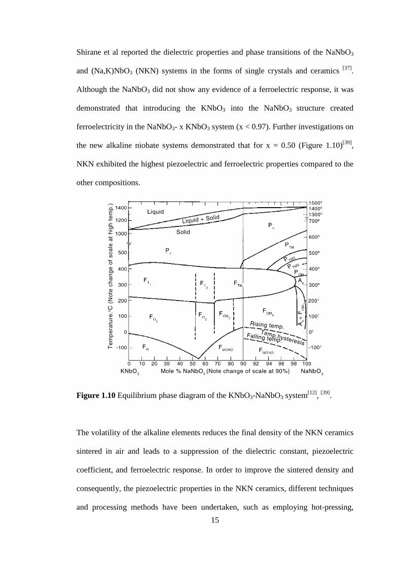
Shirane et al reported the dielectric properties and phase transitions of the NaNbO3
and (Na,K)NbO3 (NKN) systems in the forms of single crystals and ceramics [37].
Although the NaNbO3 did not show any evidence of a ferroelectric response, it was
demonstrated that introducing the KNbO3 into the NaNbO3 structure created
ferroelectricity in the NaNbO3- x KNbO3 system (x < 0.97). Further investigations on
the new alkaline niobate systems demonstrated that for x = 0.50 (Figure 1.10)[39],
NKN exhibited the highest piezoelectric and ferroelectric properties compared to the
other compositions.
Figure 1.10 Equilibrium phase diagram of the KNbO3-NaNbO3 system[12], [39].
The volatility of the alkaline elements reduces the final density of the NKN ceramics
sintered in air and leads to a suppression of the dielectric constant, piezoelectric
coefficient, and ferroelectric response. In order to improve the sintered density and
consequently, the piezoelectric properties in the NKN ceramics, different techniques
and processing methods have been undertaken, such as employing hot-pressing,

16
sintering aids, and isostatic pressing. It has been reported that hot-pressed
Na0.5K0.5NbO3 possessed high remnant polarization (Pr = 33 μC/cm2), a large
piezoelectric coefficient (d33 = 160 pC N-1) and high planar coupling factor (Kp =
0.45) [38].
Enormous efforts have been undertaken to improve the physical and electrical
properties of the NKN-based ceramics by modifying the fabrication procedure,
employing different dopants (i.e. Li1+, Ta+5, and Sb3+)[40], and combining the NKN
with other good piezoelectric materials such as BaTiO3 [41] .
It is evident that creating engineered textured structures in ceramics has led to
fascinating piezoelectric and electrical properties; however, this process requires
high cost and special facilities. Saito et al. have successfully textured a complex
Na0.5K0.5NbO3-based ceramic, (K0.44Na0.52Li0.04)(Nb0.86Ta0.10Sb0.04)O3, and achieved
the best piezoelectric coefficients in the NKN system: d33 = 416 pC N-1 and d31 = -
152 pC N-1 [42].
1.3.3 Barium titanates
Barium titanate (BaTiO3) is one of the most widely explored lead-free ferroelectric
materials, as it possesses good piezoelectric, nonlinear optical properties and voltage-
tuneable low loss dielectric properties. It experiences several phase transitions from
low temperature to high temperature, including orthorhombic-rhombohedral at ~199
K, rhombohedral-tetragonal at ~ 285 K, tetragonal-cubic at ~ 393 K, and a drastic
crystal structure transition at ~ 1733 K from perovskite to hexagonal structure before
melting at 1891 K (Figure 1.11) [43].

17
(b)
Figure 1.11 (a) Barium titanate crystalline structures at different temperatures. (b)
Dielectric constant of BaTiO3 as a function of temperature [43].
Because of its fascinating dielectric, ferroelectric, and piezoelectric properties, the
perovskite BaTiO3 has been employed in various applications, such as piezoelectric
sensors, capacitors, memories, and optical devices [12] .
The piezoelectricity in perovskite structurea such as that of BaTiO3 is due to an off-
center atom located in an octahedral position in the centre of the unit cell. In the
BaTiO3 unit cell, the Ti displacement along the polarization direction changes the
charge balance and creates an internal electric field and charge separation (Figure
1.12). Spontaneous polarization developed by the Ti displacement results in strong
piezoelectric and ferroelectric properties in the BaTiO3 and other perovskite
structures such as PZT.
Figure 1.12 (a) Tetragonal perovskite structure of BaTiO3. (b) Piezoelectric effects

18
in a BaTiO3 unit cell due to Ti displacement under an external electric field E [44].
It is well known that doping is an effective method to improve the material
performance in electroceramics. BaTiO3 doped with Ca and Zr demonstrates high
dielectric permittivity, enhanced temperature stability, and high reliability compared
to pure BaTiO3. The effects of Ca and Zr on the piezoelectric and electrical
properties of BaTiO3 will be discussed in the following section.
Effect of Zr on BaTiO3
The Zr4+ ion is dissolved in the BaTiO3 structure via a substitutionally solid solution,
where it is placed in the Ti4+ site and forms barium zirconate titanate (Ba(Ti,Zr)O3).
The Zr4+ ion (ionic radius = 87 pm) is larger and chemically more stable than the Ti+4
ion (ionic radius = 68 pm), and thus replacement of Ti+4 by Zr+4 suppresses the
conduction developed by the electronic hopping between Ti+4 and Ti+3, and leads to
an enhanced dielectric constant and reduced leakage current in the BaTiO3 structure.
The piezoelectric and electrical properties in the Ba(Ti1-xZrx)O3 system have been
investigated for different Zr concentrations, and it has been demonstrated that for
compositions 0 ≤ x ≤ 0.1 the ceramics show normal ferroelectric behaviour,
however, for compositions 0.10 ≤ x ≤ 0.42 relaxor properties are indicated. It has
been demonstrated that using a Zr/Ti ratio of 20/80 in the Ba(Ti,Zr)O3 ceramics
creates good piezoelectric and electrical properties in this system.
Effect of Ca on BaTiO3
There have been several reports indicating that partial replacement of Ba2+ by Ca2+
ions enhances the dielectric constant, piezoelectric properties, electromechanical
response, and ferroelectric properties of the BaTiO3 composition [45-48]. In the barium
calcium titanate system ((Ba1-xCax) TiO3), the piezoelectric coefficient has been

19
(a)
improved from 180 up to 310 pC N-1 for 0.02 ≤ x ≤ 0.34 [48]. The Curie temperature
is increased to 136°C by adding the Ca2+ ions up to x = 0.08 and then reduced for
higher contents. [47].
Figure 1.13 (a) Equilibrium phase diagram of the BaTiO3-CaTiO3 system [45]. (b)
Piezoelectric constants of <100>c oriented (Ba,Ca)TiO3 single crystals and zone-melt
biphasic polycrystals [48].
Recently, the lead-free pseudobinary (1-x) Ba(Zr0.20Ti0.80)O3 - x (Ba0.70Ca0.30)TiO3
system[49] has been shown to possess a very high piezoelectric response (Figure
1.14). In this system, the optimal composition with x = 0.5 at room temperature at the
morphotropic phase boundary possesses the highest piezoelectric performance: d33 =
620 pC N-1, g33 = 15.38 × 10⁻³ Vm N-1, electromechanical coupling factor K33 = 65%,
dielectric permittivity as high as εг ~ 3060, and electromechanical (converse
piezoelectric) response of 1140 pm V-1 [49, 50].
(b)
aj393
Highlight

20
Figure 1.14 (a) Hysteresis loops of 40BCT, 40BCT,and 60BCT. (b1) Saturation
polarization, Pm, (b2) remnant polarization, Pr, (b3) coercive field, Ec, (b4)
permittivity, (b5) piezoelectric coefficient, d33, and (b6) converse piezoelectric
coefficient d = S/E. Values of various PZTs are also shown as a reference. (c)
Comparison of d33 among BZT-50BCT and other non-Pb piezoelectrics, and yjr PZT
family. (d) Comparison of the electrostrain versus electric field among BZT-50BCT
and various PZTs. (e1) Temperature dependence of the direct piezoelectric
coefficient in BZT-50BCT. (e2) Temperature dependence of the direct piezoelectric
coefficient in BZT-45BCT (f) Phase diagram of pseudo-binary ferroelectric system
Ba(Zr0.20Ti0.80) O3-(Ba0.70Ca0.30)TiO3, abbreviated as BZT-BCT [49].
It was demonstrated that there was a tricritical point (TCP) in the phase diagram at x
= 0.35 and T = 57 °C. Here, the cubic-paraelectric, ferroelectric rhombohedral, and
tetragonal phases meet each other. In the vicinity of the tricritical point, the
polarization anisotropy vanishes, so that the dielectric permittivity and piezoelectric
coefficient experience very strong enhancement (Figure 1.15). The piezoelectric
parameter is comparable to 500-600 pC N-1 in PZT and considerably higher than
(f)

21
(a)
those in Pb-free piezoelectric compositions such as alkaline niobate ceramics with
300 pC N-1 [42] and bismuth based layered ferroelectric compositions with about 100
pC N-1 [27]. The high piezoelectric performance was obtained in bulk BTZ-BCT
ceramic, which makes it a promising candidate in piezoelectric devices.
Figure 1.15 (a) Schematic illustration of the tilted MPB developed in the BZT-xBCT
system. Point b represents the TCP and c, d, and e identify three different molar
ratios x at different temperatures along the MPB. (b),(c),(d), and (e) represent the 1D
free energy barrier plot against the polarization rotation from rhombohedral (PR) to
tetragonal (PT) and vice versa. (f) Dielectric constant vs. temperature change in
Ba(Zr0.15Ti0.85)O3 (rhombohedral phase) and (Ba0.80Ca0.20)TiO3 (tetragonal phase) [51].
1.3.4 Other lead-free piezoelectric materials
There are other lead-free piezoelectric materials including wurtzite structures and
quartz (Figure 1.16), which are not ferroelectric. The piezoelectric behaviour in this
group has been discussed previously. Thus, they are employed either as single
crystals or as oriented polycrystalline samples and textured thin films.
(f)
(b) (c) (d) (e)
22
Figure 1.16 ZnO unit cell in the wurtzite structure [52].
Although most of them exhibit low piezoelectric performance, their stability and
compatibility in terms of integration into electronic systems have caused them to
emerge as useful piezoelectric materials in electronic devices. The most commonly
studied materials in this group are ZnO , AlN, and GaN in the forms of textured thin
films and single crystals [52-55]. Their piezoelectric coefficients are compared in Table
1.3.
Table 1.3 Piezoelectric coefficients of ZnO, AlN, and GaN in the forms of thin films
and single crystal.
Materials d33 (pm V-1)
Ref. Single crystal Thin film
ZnO 3.0 4.41 [54]
AlN 5.6 3.4 [55]
GaN 3.7 2.8 [53]
1.4 Low-dimensional piezoelectric properties measurements
Scanning probe microscopy (SPM) techniques, such as Kelvin probe force
microscopy (KPFM), scanning tunnelling microscopy (STM), scanning capacitance
microscopy (SCM), scanning spreading resistance microscopy (SSRM), and
piezoresponse force microscopy (PFM) have emerged as powerful tools to study

23
surface electrical properties, ferroelectric domains, and the piezoelectric response in
low-dimensional materials [56-62].
Figure 1.17 (a) Schematic illustration of the PFM experimental set up. (b) Surface
displacement of a piezoelectric sample due to the inverse piezoelectric effect
exhibited by the ferroelectric domains under applied electric field.
PFM has been established as a reliable approach to study the dynamic behaviour,
piezoelectric properties, switching mechanism, and configuration of the ferroelectric
domains in the piezoelectric materials. This technique is based on the contact-mode
in SPM, for which the instrument is equipped with a function generator, lock-in
amplifier, and a conductive cantilever [63-70]. Figure 1.17 schematically illustrates the
PFM setup.
(a)
(b)

24
The piezoelectric response of the surface is acquired by applying DC and AC
voltages to the tip scanning over the surface in the contact mode:
Vtip = Vdc + Vac cos(ωt) (1.11) [63]
Where the electric AC component causes deformation of the surface through the
converse piezoelectric effect, and leading to the tip deflection (Figure 1.18) as
follows:
d = d0 + A 𝑐𝑜𝑠(𝜔𝑡 + 𝜑) (1.12) [71]
Where A represents the amplitude of the piezoelectric response and φ defines the
phase shift generated by the ferroelectric domain located below the tip. The different
configurations of the ferroelectric domains include parallel to the sample surface (in-
plane or a-domain) and vertical with respect to the sample surface (out-of-plane or c-
domain) (Figure 1.18(a)). Lateral and vertical displacements are created by in-plane
and out-of-plane domains, respectively. Since the tip is in contact with the surface of
the sample, all types of domains exhibit corresponding movements in the tip,
consisting of vertical, longitudinal and lateral movements. Considering the vertical
and lateral movement of the tip (as longitudinal movement is objected in vertical
displacement), vertical PFM (VPFM) and lateral PFM (LPFM) have been developed
to study the in-plane and out-of-plane ferroelectric domains [72].

25
Figure 1.18(a) Schematic illustration of the a-domains and c-domains in a crystal.
(b) Possible movements of the cantilever due to a force developed by the interaction
of different domains with the applied AC signal, in which Fdefl results in deflection,
Fbuck leads to buckling, and Ftor creates torsion in the cantilever. (c) Side- and top-
view of the cantilever movement. (d) Possible movements of the laser spot on the
photo detector. Fdefl and Fbuck result in a vertical signal, while only Ftor results in a
lateral signal [70]
1.5 Research motivation
Low-dimensional ferroelectric materials, including nanofibers, nanotubes,
nanowires, nanobelts, and thin films, have emerged as a hot research topic due to
their novel properties and applications. The state-of-the-art piezoelectric bulk
materials, such as PZT, which have the best piezoelectric performance among all the
piezoelectric compounds, have been used practically as key components in electronic
sensors, actuators, transducers, electro-mechanical energy conversion devices, etc.
Integration of high performance piezoelectrics in piezoelectric devices and
micro/nano electromechanical systems (MEMS, NEMS) is a viable approach to
enhance their efficiency. Low-dimensional piezoelectric and ferroelectric materials
(a) (b) (c)
(d)

26
have been exploited widely in nanogenerators, sensors, transducers, MEMS devices,
and other applications such as microwave varactors and ferroelectric field effect
transistors.[73-78] For instance, high performance piezoelectric nanostructures can
enhance the output power of piezoelectric generators that convert kinetic energy of
vibrations, displacements, or applied force to electricity.[79-83]
There are three challenging issues, however, that need to be addressed for
nanostructured piezoelectric materials and their devices: 1) Although scaling down
the devices to the nanoscale provides significant benefits such as suppressing the
energy consumption, the ferroelectric and piezoelectric properties are often
suppressed in small dimensions due to intrinsic or extrinsic effects, depending on
such factors as lateral size, geometry, particle size, fraction of parallel (a-domains)
and perpendicular (c-domains) domains on the surface, in-plane stress, and domain
wall mobility. 2) Confinement of the nanosized piezoelectric components by the
substrate develops internal stress in its interface with the substrate (clamping effect),
which results in a suppression of its piezoelectric performance. 3) Although
piezoeloectric single crystals possess remarkably high piezoelectric coefficients,
growing single crystals on the nanoscale such as in nanowires and
nanorods/nanoribbons, while retaining their superior performance, is very difficult in
practice due to complex phase formation dynamics, in particular for ternary
piezoelectric systems.
Enormous efforts have been undertaken to find innovative new materials and
improve the piezoelectric response by varying their compositions and shapes in the
form of thin films, nanowires, and nanofibers. To the best of our knowledge,
however, the piezoelectric response reported for the polycrystalline nanostructured
materials, so far, has been less than 160 pm V-1 [58, 84-94] Grain boundaries create

27
pinning sites for ferroelectric domain wall motion. The high density of grain
boundaries restricts domain wall mobility in nanostructured materials. As a
consequence, the electromechanical response becomes smaller compared to bulk
ceramics containing coarse grains and single crystals, with a lower density of grain
boundaries.[95]
Recently, a lead-free Ba(Ti0.80Zr0.20)O3-x(Ba0.70Ca0.30)TiO3 ((1-x)BTZ-xBCT)
piezoelectric system with optimal composition x = 0.5 was reported to show superior
room temperature piezoelectricity, with the piezoelectric coefficient d33 = 620 pC N-
1, the piezoelectric voltage constant g33 = 15.38×10⁻³ Vm N-1, and the
electromechanical (converse piezoelectric) response as high as 1140 pm V-1. These
superior piezoelectric properties are comparable to or higher than those of state-of-
the-art PZT or other lead-free piezoelectric compounds, due to the low polarization
anisotropy and low energy barrier for lattice distortions in the MPB region.[49] The
large d33 obtained in bulk BTZ-BCT ceramics makes this compound a promising
candidate as a component for low-dimensional piezoelectric devices. It is expected
that nanowires/nanofibers or thin films of this compound should have better
piezoelectric properties than that of any existing piezoelectric materials.
In this research, two different aspects of the low dimensional piezoelectric materials
were investigated.
First, low-dimensional counterparts of BTZ-BCT in forms of thin films and
nanofibers were synthesized, and their structures and their piezoelectric and
ferroelectric properties were investigated and compared with the BTZ-BCT
ceramics. Different scanning probe microscopy techniques, including atomic force
microscopy (AFM), piezoresponse force microscopy (PFM), scanning capacitance
microscopy (SCM), and scanning spreading resistance microscopy (SSRM) were

28
employed to study the piezoelectric, ferroelectric, and electric properties of the thin
films and nanofibers. Then, biocompatible NKN nanofibers as a piezoelectric
scaffold was synthesized and characterized.
1.6 References
[1] B. Jaffe, Cook W.R. Jr., J. H.L., Piezoelectric Ceramics, Academic Press
Inc., 1971.
[2] A. Safari, E. K. Akdoğan, Piezoelectric and Acoustic Materials for
Transducer Applications, Springer London, Limited, 2008.
[3] D. Ensminger, F. B. Stulen, Ultrasonics: Data, Equations and Their
Practical Uses, Taylor & Francis, 2010.
[4] G. Shirane, J. D. Axe, J. Harada, J. P. Remeika, Phys. Rev. B 1970, 2, 155.
[5] E. Lines, A. M. Glass, Principles and Applications of Ferroelectrics and
Related Materials, OUP Oxford, 1977.
[6] K. Kushida, H. Takeuchi, Appl. Phys. Lett. 1987, 50, 1800.
[7] F. M. Pontes, D. S. L. Pontes, E. R. Leite, E. Longo, E. M. S. Santos, S.
Mergulhao, A. Chiquito, P. S. Pizani, F. Lanciotti, T. M. Boschi, J. A. Varela, J.
Appl. Phys. 2002, 91, 6650.
[8] R. Poyato, x, M. L. Calzada, L. Pardo, Appl. Phys. Lett. 2004, 84, 4161.
[9] H. Schmitt, J. Mendiola, F. Carmona, C. Alemany, B. Jimenez,
Microelectron. Eng. 1995, 29, 181.
[10] H. Takeuchi, S. Jyomura, C. Nakaya, "Highly Anisotropic Piezoelectric
Ceramics and Their Application in Ultrasonic Probes", presented at IEEE 1985
Ultrasonics Symposium, 16-18 Oct. 1985, 1985.
[11] C. Kittel, Physical Review 1951, 82, 729.

29
[12] B. Jaffe, Piezoelectric Ceramics, Elsevier Science, 1971.
[13] C. A. Randall, N. Kim, J.-P. Kucera, W. Cao, T. R. Shrout, J. Am. Ceram.
Soc. 1998, 81, 677.
[14] B. Noheda, D. E. Cox, G. Shirane, J. A. Gonzalo, L. E. Cross, S. E. Park,
Appl. Phys. Lett. 1999, 74, 2059.
[15] S. Mabud, J. Appl. Crystallogr. 1980, 13, 211.
[16] P. Ari-Gur, L. Benguigui, Solid State Commun. 1974, 15, 1077.
[17] R. Guo, L. E. Cross, S. E. Park, B. Noheda, D. E. Cox, G. Shirane, Phys. Rev.
Lett. 2000, 84, 5423.
[18] D. Damjanovic, Appl. Phys. Lett. 2010, 97, 062906.
[19] M. Budimir, D. Damjanovic, N. Setter, Phys. Rev. B 2006, 73, 174106.
[20] M. Ahart, M. Somayazulu, R. E. Cohen, P. Ganesh, P. Dera, H.-k. Mao, R. J.
Hemley, Y. Ren, P. Liermann, Z. Wu, Nature 2008, 451, 545.
[21] M. Pastor, P. K. Bajpai, R. N. P. Choudhary, Bull. Mater. Sci. 2005, 28, 199.
[22] J. Kuwata, K. Uchino, S. Nomura, Ferroelectrics 1981, 37, 579.
[23] A. Halliyal, A. Safari, Ferroelectrics 1994, 158, 295.
[24] E. K. Akdogan, A. Hall, W. K. Simon, A. Safari, J. Appl. Phys. 2007, 101,
024104.
[25] G. Robert, M. Demartin, D. Damjanovic, J. Am. Ceram. Soc. 1998, 81, 749.
[26] Y. Yamashita, K. Harada, T. Tao, N. Ichinose, Integrated Ferroelectrics
1996, 13, 9.
[27] J. Rödel, W. Jo, K. T. P. Seifert, E.-M. Anton, T. Granzow, D. Damjanovic,
J. Am. Ceram. Soc. 2009, 92, 1153.
[28] H. S. Shulman, M. Testorf, D. Damjanovic, N. Setter, J. Am. Ceram. Soc.
1996, 79, 3124.

30
[29] T. Takenaka, H. Nagata, J. Eur. Ceram. Soc. 2005, 25, 2693.
[30] Y. Noguchi, M. Miyayama, Appl. Phys. Lett. 2001, 78, 1903.
[31] T. Takenaka, K. Sakata, Ferroelectrics 1991, 118, 123.
[32] Y. Li, W. Chen, J. Zhou, Q. Xu, H. Sun, R. Xu, Materials Science and
Engineering: B 2004, 112, 5.
[33] C. Zhou, X. Liu, J Mater Sci 2008, 43, 1016.
[34] P. K. Panda, J Mater Sci 2009, 44, 5049.
[35] K. M. T. Takenaka, K. Sakata, , Jpn. J. Appl. Phys., Part 1 1991, 30, 4.
[36] X. X. Wang, H. L. W. Chan, C. L. Choy, Appl. Phys. A 2005, 80, 333.
[37] G. Shirane, R. Newnham, R. Pepinsky, Physical Review 1954, 96, 581.
[38] R. E. Jaeger, L. Egerton, J. Am. Ceram. Soc. 1962, 45, 209.
[39] E. Ringgaard, T. Wurlitzer, J. Eur. Ceram. Soc. 2005, 25, 2701.
[40] N. Marandian Hagh, B. Jadidian, A. Safari, J. Electroceram. 2007, 18, 339.
[41] Y. T. Lu, X. M. Chen, D. Z. Jin, X. Hu, Mater. Res. Bull. 2005, 40, 1847.
[42] Y. Saito, H. Takao, T. Tani, T. Nonoyama, K. Takatori, T. Homma, T.
Nagaya, M. Nakamura, Nature 2004, 432, 84.
[43] A. von Hippel, Reviews of Modern Physics 1950, 22, 221.
[44] T. Ryoko, F. Desheng, I. Mitsuru, D. Masahiro, K. Shin-ya, J. Phys.:
Condens. Matter 2009, 21, 215903.
[45] M.-S. Yoon, S.-C. Ur, Ceram. Int. 2008, 34, 1941.
[46] D. Fu, M. Itoh, S.-y. Koshihara, T. Kosugi, S. Tsuneyuki, Phys. Rev. Lett.
2008, 100, 227601.
[47] T. Mitsui, W. B. Westphal, Physical Review 1961, 124, 1354.
[48] D. Fu, M. Itoh, S.-y. Koshihara, Appl. Phys. Lett. 2008, 93, 012904.
[49] W. Liu, X. Ren, Phys. Rev. Lett. 2009, 103, 257602.

31
[50] D. Xue, Y. Zhou, H. Bao, C. Zhou, J. Gao, X. Ren, J. Appl. Phys. 2011, 109,
054110.
[51] B. Huixin, Z. Chao, X. Dezhen, G. Jinghui, R. Xiaobing, J. Phys. D: Appl.
Phys. 2010, 43, 465401.
[52] R. Prashanth, K. Sriram, R. Siddharth, N. W. Gregory, Smart Mater. Struct.
2012, 21, 094003.
[53] I. L. Guy, S. Muensit, E. M. Goldys, Appl. Phys. Lett. 1999, 75, 4133.
[54] D. A. Scrymgeour, T. L. Sounart, N. C. Simmons, J. W. P. Hsu, J. Appl.
Phys. 2007, 101, 014316.
[55] M.-A. Dubois, P. Muralt, Appl. Phys. Lett. 1999, 74, 3032.
[56] P. Eyben, F. Seidel, T. Hantschel, A. Schulze, A. Lorenz, A. U. De Castro, D.
Van Gestel, J. John, J. Horzel, W. Vandervorst, physica status solidi (a) 2011, 208,
596.
[57] X. Ou, P. D. Kanungo, R. Kögler, P. Werner, U. Gösele, W. Skorupa, X.
Wang, Nano Lett. 2009, 10, 171.
[58] A. Bernal, A. Tselev, S. Kalinin, N. Bassiri-Gharb, Adv. Mater. 2012, 24,
1159.
[59] Y. Kim, C. Bae, K. Ryu, H. Ko, Y. K. Kim, S. Hong, H. Shin, Appl. Phys.
Lett. 2009, 94, 032907.
[60] J. Y. Son, S. H. Bang, J. H. Cho, Appl. Phys. Lett. 2003, 82, 3505.
[61] L. Y. Kraya, R. Kraya, J. Appl. Phys. 2012, 111, 013708.
[62] N. Nobuyuki, Y. Takuma, S. Hiroyuki, S. Yoshihiko, M. Masayuki, W.
Shunji, Nanotechnology 1997, 8, A32.
[63] J. Stephen, P. B. Arthur, V. K. Sergei, Nanotechnology 2006, 17, 1615.
32
[64] S. V. Kalinin, A. Gruverman, Scanning Probe Microscopy Electrical and
Electromechanical Phenomena at the Nanoscale: Fundamentals and Applications,
Springer Science+Business Media, LLC, 2007.
[65] E. B. Araujo, E. C. Lima, I. K. Bdikin, A. L. Kholkin, J. Appl. Phys. 2013,
113, 187206.
[66] Y. Liu, K. H. Lam, K. K. Shung, J. Li, Q. Zhou, J. Appl. Phys. 2013, 113,
187205.
[67] V. Y. Shur, E. A. Mingaliev, V. A. Lebedev, D. K. Kuznetsov, D. V. Fursov,
J. Appl. Phys. 2013, 113, 187211.
[68] F. Borodavka, I. Gregora, A. Bartasyte, S. Margueron, V. Plausinaitiene, A.
Abrutis, J. Hlinka, J. Appl. Phys. 2013, 113, 187216.
[69] A. N. Morozovska, E. A. Eliseev, O. V. Varenyk, S. V. Kalinin, J. Appl.
Phys. 2013, 113, 187222.
[70] S. Elisabeth, J. Phys. D: Appl. Phys. 2011, 44, 464003.
[71] S. V. Kalinin, D. A. Bonnell, Phys. Rev. B 2002, 65, 125408.
[72] B. J. Rodriguez, A. Gruverman, A. I. Kingon, R. J. Nemanich, J. S. Cross, J.
Appl. Phys. 2004, 95, 1958.
[73] Z. L. Wang, J. Song, Science 2006, 312, 242.
[74] M. Bhaskaran, S. Sriram, S. Ruffell, A. Mitchell, Adv. Funct. Mater. 2011,
21, 2251.
[75] S. C. Masmanidis, R. B. Karabalin, I. De Vlaminck, G. Borghs, M. R.
Freeman, M. L. Roukes, Science 2007, 317, 780.
[76] P. Muralt, J. Micromech. Microeng. 2000, 10, 136.
[77] C.-R. Cho, J.-H. Koh, A. Grishin, S. Abadei, S. Gevorgian, Appl. Phys. Lett.
2000, 76, 1761.

33
[78] S.-M. Koo, S. Khartsev, C.-M. Zetterling, A. Grishin, M. Ostling, Appl. Phys.
Lett. 2003, 83, 3975.
[79] K.-I. Park, M. Lee, Y. Liu, S. Moon, G.-T. Hwang, G. Zhu, J. E. Kim, S. O.
Kim, D. K. Kim, Z. L. Wang, K. J. Lee, Adv. Mater. 2012, 24, 2999.
[80] X. Chen, S. Xu, N. Yao, Y. Shi, Nano Lett. 2010, 10, 2133.
[81] Y. Hu, Y. Zhang, C. Xu, G. Zhu, Z. L. Wang, Nano Lett. 2010, 10, 5025.
[82] H. D. Espinosa, R. A. Bernal, M. Minary-Jolandan, Adv. Mater. 2012, 24,
4656.
[83] B. J. Hansen, Y. Liu, R. Yang, Z. L. Wang, ACS Nano 2010, 4, 3647.
[84] M. Fan, W. Hui, Z. Li, Z. Shen, H. Li, A. Jiang, Y. Chen, R. Liu,
Microelectron. Eng. 2012, 98, 371.
[85] J. Wang, J. B. Neaton, H. Zheng, V. Nagarajan, S. B. Ogale, B. Liu, D.
Viehland, V. Vaithyanathan, D. G. Schlom, U. V. Waghmare, N. A. Spaldin, K. M.
Rabe, M. Wuttig, R. Ramesh, Science 2003, 299, 1719.
[86] J. J. Urban, W. S. Yun, Q. Gu, H. Park, J. Am. Chem. Soc. 2002, 124, 1186.
[87] J. J. Urban, J. E. Spanier, L. Ouyang, W. S. Yun, H. Park, Adv. Mater. 2003,
15, 423.
[88] L. Sagalowicz, F. Chu, P. D. Martin, D. Damjanovic, J. Appl. Phys. 2000, 88,
7258.
[89] P. M. Rørvik, T. Grande, M.-A. Einarsrud, Adv. Mater. 2011, 23, 4007.
[90] Y. Guo, K. Suzuki, K. Nishizawa, T. Miki, K. Kato, J. Cryst. Growth 2005,
284, 190.
[91] A. L. Kholkin, M. L. Calzada, P. Ramos, J. Mendiola, N. Setter, Appl. Phys.
Lett. 1996, 69, 3602.

34
[92] S. Fujino, M. Murakami, V. Anbusathaiah, S. H. Lim, V. Nagarajan, C. J.
Fennie, M. Wuttig, L. Salamanca-Riba, I. Takeuchi, Appl. Phys. Lett. 2008, 92,
202904.
[93] Y. Q. Chen, X. J. Zheng, X. Feng, Nanotechnology 2010, 21, 055708.
[94] S. H. Xie, J. Y. Li, Y. Qiao, Y. Y. Liu, L. N. Lan, Y. C. Zhou, S. T. Tan,
Appl. Phys. Lett. 2008, 92, 062901.
[95] A. Gruverman, A. Kholkin, Rep. Prog. Phys. 2006, 69, 2443.

35
Chapter 2. BTZ-BCT Ceramics
In this chapter, the impact of lattice parameters variations on the ferroelectric
properties in the barium titanate zirconate ─ barium calcium titanate ( (1-x)BTZ-
xBCT) system is investigated.
2.1 Introduction
Ferroelectricity in crystalline structures intrinsically is created by the electric dipole
developed by an off-centre atom located in the unit cell. Any change in the lattice
parameters can alter the electric dipole moment in the unit cell and consequently
changes the ferroelectric response. Several factors, such as doping, temperature
variation, crystal defects, internal/external strain, and electric field, can induce the
deformation in the unit cell which results in an enhancement or suppression of the
ferroelectric properties in the crystalline structures.
Several studies have been undertaken to explore the piezoelectric, pyroelectric, and
electromechanical properties of Ba (Ti0.8Zr0.2)TiO3- (Ba0.7Ca0.3)TiO3 (BTZ-BCT)
since it was introduced as a promising lead-free piezoelectric and ferroelectric
compound [1-6]. Since the (1-x)BTZ-xBCT system shows ferroelectricicity in addition
to piezoelectricity, a detailed study on the ferroelectricity and the compositional
dependency in this system is very much indicated. In this Chapter, the effects of Zr
and Ca on the lattice parameters and ferroelectric properties in the (1-x)BTZ-xBCT
system are investigated.
aj393
Highlight
aj393
Highlight
aj393
Highlight
aj393
Highlight

36
2.2 Experimental procedure
(1-x)Ba(Ti0.8Zr0.2)TiO3-x(Ba0.7Ca0.3)TiO3 ((1-x)BTZ-xBCT) ceramics with x = 0.0,
0.1,0.2,0.3,0.4,0.5 were prepared using the conventional solid-state reaction method.
BaCO3, CaCO3, TiO2, and ZrO2 were used as raw materials. Stoichiometric ratios of
the materials were mixed via planetary ball milling. Zirconia balls were used, and
distilled water was employed as the ball-milling medium to increase the efficiency.
The resultant slurries were dried in an oven at 100oC for 12 hrs. The mixed powders
were pressed into disks 12 mm in diameter and 3 mm in thickness under 150 MPa
using a uniaxial pressure and calcined at 1300°C for 2 h. Sintering of samples was
carried out at 1450°C for 2 h in the air. The polished surfaces of the samples were
coated with silver paste for electrical and piezoelectric measurements. The crystal
structure and phase content of the ceramics were studied by X-ray diffraction (XRD;
GBC MMA, CuKα radiation, 40 kV, 25 mA) and Raman spectroscopy (HORIBA
Jobin Yvon, HR800) using a He-Ne laser with 632.8 nm wavelength. A field
emission scanning electron microscope (FE-SEM, JEOL JSM 7500FA) was used to
study the morphology and particle size in the ceramics. The electric field dependence
of the polarization (P vs. E dependence) of the ceramics was measured using an HP
42980 LCR-meter. The piezoelectric coeffcient d33 of the ceramics were measured
using a d33 meter ( YE2730A, APC International. Ltd.) at room temperature.
2.3 Results and discussions
2.3.1 Crystalline structure and vibration modes
Figure 2.1 shows XRD patterns of (1-x)BTZ-xBCT ceramics with x = 0.1, 0.2, 0.3,
0.4, and 0.5 molar ratios sintered at 1450°C for 2 h in the air. The XRD patterns
indicate that all samples were fully crystallized in a perovskite structure. Introducing
aj393
Highlight
aj393
Highlight
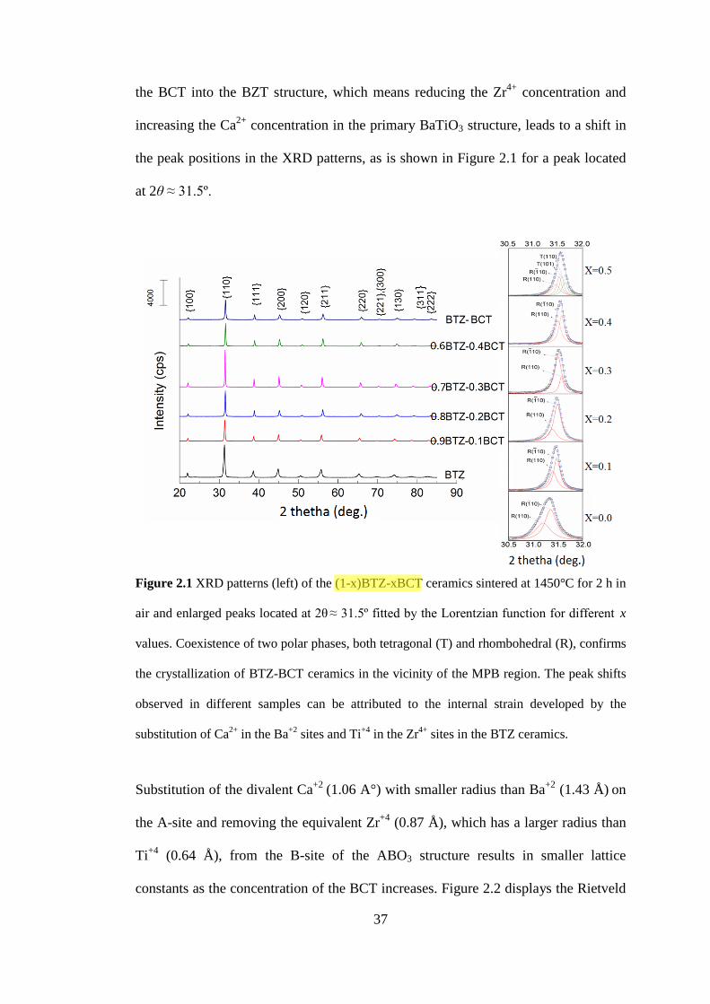
37
the BCT into the BZT structure, which means reducing the Zr4+ concentration and
increasing the Ca2+ concentration in the primary BaTiO3 structure, leads to a shift in
the peak positions in the XRD patterns, as is shown in Figure 2.1 for a peak located
at 2θ ≈ 31.5º.
Figure 2.1 XRD patterns (left) of the (1-x)BTZ-xBCT ceramics sintered at 1450°C for 2 h in
air and enlarged peaks located at 2θ ≈ 31.5º fitted by the Lorentzian function for different x
values. Coexistence of two polar phases, both tetragonal (T) and rhombohedral (R), confirms
the crystallization of BTZ-BCT ceramics in the vicinity of the MPB region. The peak shifts
observed in different samples can be attributed to the internal strain developed by the
substitution of Ca2+ in the Ba+2 sites and Ti+4 in the Zr4+ sites in the BTZ ceramics.
Substitution of the divalent Ca+2 (1.06 A°) with smaller radius than Ba+2 (1.43 Å) on
the A-site and removing the equivalent Zr+4 (0.87 Å), which has a larger radius than
Ti+4 (0.64 Å), from the B-site of the ABO3 structure results in smaller lattice
constants as the concentration of the BCT increases. Figure 2.2 displays the Rietveld
aj393
Highlight
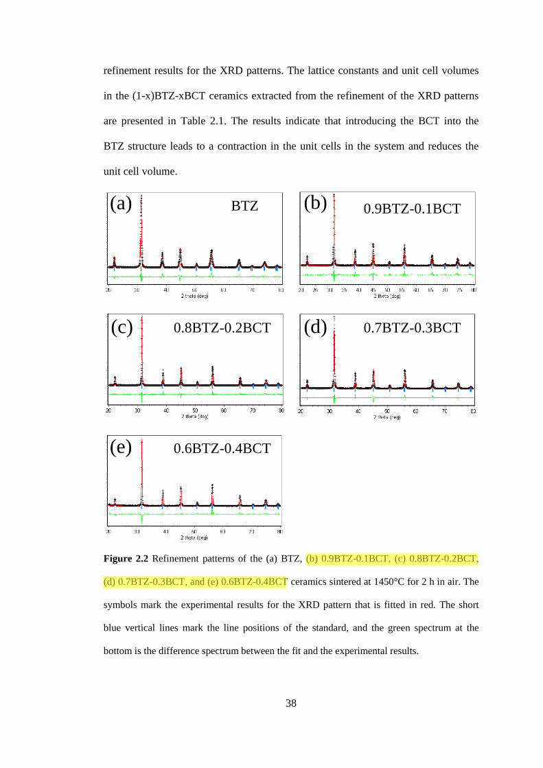
38
refinement results for the XRD patterns. The lattice constants and unit cell volumes
in the (1-x)BTZ-xBCT ceramics extracted from the refinement of the XRD patterns
are presented in Table 2.1. The results indicate that introducing the BCT into the
BTZ structure leads to a contraction in the unit cells in the system and reduces the
unit cell volume.
Figure 2.2 Refinement patterns of the (a) BTZ, (b) 0.9BTZ-0.1BCT, (c) 0.8BTZ-0.2BCT,
(d) 0.7BTZ-0.3BCT, and (e) 0.6BTZ-0.4BCT ceramics sintered at 1450°C for 2 h in air. The
symbols mark the experimental results for the XRD pattern that is fitted in red. The short
blue vertical lines mark the line positions of the standard, and the green spectrum at the
bottom is the difference spectrum between the fit and the experimental results.
BTZ (a) (b) 0.9BTZ-0.1BCT
(c) 0.8BTZ-0.2BCT (d) 0.7BTZ-0.3BCT
(e) 0.6BTZ-0.4BCT
aj393
Highlight

39
Crystal structures in the ceramics were determined by analysing of the intense peak
located at 2θ ≈ 31.5º in the XRD patterns of all the samples (Figure 2.1).
A Lorentzian peak fitting function was employed to study the crystalline phase
configuration and changes in the samples. It is demonstrated that by increasing the
BCT in the system, the primary structure experiences more distortion and lattice
changes, which are reflected in the XRD peak positions and full-width-half-
maximum values (FWHMs) for the peaks in the samples. Evolution of the tetragonal
structure in the BTZ-BCT ceramics is evident in Figure 2.1.
The coexistence of two ferroelectric phases, the tetragonal and rhombohedral,
enhances the polarizability of the system and elininates the energy barrier against
switching of the polarization direction [1]. Crystallization in the vicinity of the
morphotropic phase boundary (MPB) and approaching the triple critical point (TCP)
in the BTZ-BCT ceramic dramatically improve its piezoelectric and ferroelectric
properties, as reported earlier by Liu et.al. [1].
Field emission scanning electron microscope images of the BTZ-BCT ceramic are
shown in Figure 2.3 (a) and (b). The images were tcollected without a conducting
coating to preserve the inherent topography of the grains. Figure2.3 (a) shows
diverse particle sizes ranging from the submicron to about 3 µm. Different crystal
defects such as edge and screw dislocations form suitable sites for the crystal growth
in BTZ-BCT ceramic. Figure 2.3(b) displays the growth steps on grains.
aj393
Highlight
aj393
Highlight

40
Table 2.1 Lattice parameters and unit cell volumes of the (1-x)BTZ-xBCT ceramics
extracted from the Rietveld refinement results on the ceramics.
X= 0 X= 0.1 X= 0.2 X= 0.3 X= 0.4 X= 0.5*
Symmetry R3m R3m R3m R3m R3m R3m P4mm
Lattice
constants
a, b, c (Å) 4.043 4.034 4.029 4.016 4.009 4.000 3.998,
4.016
α (deg.) 89.72 89.87 89.93 89.97 89.90 89.97 90.00
Unit cell
volume (Å3)
66.08 65.64 65.41 64.77 64.44 64.11
Atomic
positions
(Ba, Ca)
x 0.0 0.0 0.0 0.0 0.0 -
y 0.0 0.0 0.0 0.0 0.0 -
z 0.0 0.0 0.0 0.0 0.0 -
(Ti, Zr)
x 0.4872 0.4850 0.4995 0.4893 0.4872 -
y 0.4872 0.4850 0.4995 0.4893 0.4872 -
z 0.4872 0.4850 0.4995 0.4893 0.4872 -
O
x 0.5109 0.5131 0.5152 0.5364 0.5109 -
y 0.5109 0.5131 0.5152 0.5364 0.5109 -
z 0.0193 -0.0251 -0.0312 0.0301 0.0193 -
Rwpa 15.47 18.63 19.19 16.83 19.45 -
GOFb 3.29 2.26 2.46 3.94 2.84 -
a) The R-weighted pattern (Rwp) is used to estimate the agreement between the observations and the
model during the course of the refinement (5% < Rwp < 10%: very good agreement; 10% < Rwp <
20%: typical).
b) Goodness of fitting (GOF).
*Lattice parameters and unit cell volume were calculated using corresponding equations for the
tetragonal and rhombohedral structures [7].
aj393
Highlight

41
Figure 2.3 (a) FE-SEM image of the particle size distribution and morphology of the grains
in the BTZ-BCT ceramic sintered at 1450°C for 2 h in the air. (b) Higher magnification
image of the area indicated by the square in (a) that shows the growth steps in individual
grains.
Different vibration modes in the (1-x)BTZ-xBCT system were investigated by
Raman spectroscopy at room temperature (Figure 2.4). Spectra of the ceramics are
compared with BaTiO3 as their primary structure.
Figure 2.4 Different vibration modes in the (1-x)BTZ-xBCT system were investigated by
Raman spectroscopy at room temperature.
aj393
Highlight
aj393
Highlight

42
All features characteristic of the perovskite structure of the bulk BaTiO3 can be
verified in the Raman spectra of all the ceramics [8, 9] .
According to the vibration modes in BaTiO3, the Raman peaks located at about 520
and 724 cm-1 are generated by the (Ba,Ca)—O bonds, and the peaks at about 300 cm-
1 are due to the (Ti,Zr)—O bond vibrations in the (1-x)BTZ-xBCT system [8-10].
According to the ionic radii of the elements that exist in the system, increasing the
amount of Ca2+, with an ionic radius smaller than its host ion, Ba2+, in unit cells leads
to shorter (Ba, Ca)—O bonds, and higher vibration frequencies and a blue shift in the
bands located at about 520 and 724 cm-1. By increasing the BCT concentration in the
system, the concentration of the Zr4+, which has a larger ionic radius compared to
Ti4+, decreases, and a red shift in the band generated by the (Ti,Zr)—O bonds occurs.
2.3.2 Ferroelectric and piezoelectric properties
In order to study the ferroelectric properties of the ceramics, the polarization versus
electric field (P-E loop) changes of the bulk ceramics were studied. Generally, the
switching of the spontaneous polarizations in ferroelectrics yields a hysteresis loop
when they are imposed by a strong enough alternating electric field from positive to
negative. Figure 2.5 illustrates a typical P-E loop in a ferroelectric material. When an
electric field is applied to a ferroelectric crystal, in the OA part, the spontaneously
polarized ferroelectric domains begin to rotate, but they do not enter a permanent
state due to the weak electric field and behave similarly to a typical dielectric
material.
aj393
Highlight

43
Figure 2.5 Typical polarization versus electric field hysteresis loop (P-E loop) in a
ferroelectric material[11].
As the electric field is increased, a dramatic enhancement occurs (AB) in the
allignment of the domains, which reaches a maximum at point C. In this state, almost
all of the domains are aligned in the direction of the electric field (but with the
opposite polarity) and net polarization in the system is at its saturation level. This
value of the polarization is called the saturation polarization (OE). Even when the
electric field is then reduced to zero, a part of the aligned domains keep their
arrangement and a remanent polarization (Pr) at zero electric field is achieved (OD).
Rotation of the domains continues by reversing the electric field, and a similar
phenomenon can be seen in the opposite arrangment. The required electric field for
switching the spontaneous polarization/ferroelectric domains is called the coercive
field (OF) which exists for both positive and negative electric fields. The G and H
points in the negative region correspond to the C and D points in the positive region.
In order to investigate the effects of Zr and Ca variations on the ferroelectric
properties of the (1-x)BTZ-xBCT, system the P-E loops of the ceramics were
collected at 100 Hz sweep of the electric field. Figure 2.6(a) demonstrates that the
maximum or saturation polarization (Ps) is increased by introducing the BCT into the
aj393
Highlight

44
BTZ structure, and rthe maximum Ps= 13.32 μC cm-2 at x = 0.5 in the (1-x)BTZ-
xBCT system.
The composition dependence of the polarization elements leads to an enhancement of
about two times in the BTZ-BCT ceramic compared to the BTZ (Ps = 6.96 μC cm-2)
under the same electric field.
The correlation between the spontaneous polarization Ps and the volume of the unit
cell is as follows:
𝑃𝑠 = 1𝑣
∑ 𝛿𝑖𝑖 𝑍𝑖 (2.1)
Where 𝑣 is the unit cell volume, 𝛿𝑖 is the displacement of an atom 𝑖 from a
centrosymmetric site in the unit cell, and 𝑍𝑖 is the effective nuclear charge of tatom 𝑖.
Reducing the bonding distances in the Ba—O and Zr—O bonds, as was discussed
earlier, in the (1-x)BTZ-xBCT system by Ca2+ and Ti4+ replacements results in a
shrinkage in the unit cell volume and provides more space (Ti4+ has a smaller ionic
radius compared to Zr4+) for the displacement of an off-centre atom inside the unit
cell, and therefore, according to Equation (2.1), the spontaneous polarization
increases with substitution of the Ba2+ and Zr4+ ions by Ca2+ and Ti4+.
aj393
Highlight

45
Figure 2.6 (a) Maximum polarization Ps is increased by introducing BCT into the BTZ
structure, and the maximum Ps= 13.32 μC cm-2 at x = 0.5 in the (1-x)BTZ-xBCT system. (b)
Correlation of the polarization saturation enhancement with the decrease in the unit cell
volume in the (1-x)BTZ-xBCT ceramics. (c) The BTZ-BCT ceramic achieved the maximum
spontaneous polarization Ps = 13.86 μC cm-2 under an electric field E = 40 kV cm-1 at room
temperature. (d) Piezoelectric response enhancement in the BTZ-BCT ceramic compared to
other compositions in this system.
Figure 2.6(b) displays the correlation between the polarization saturation
enhancement and the decrease in the unit cell volume in the (1-x)BTZ-xBCT
ceramics. It must be taken into the account that approaching the MPB in the BTZ-
BCT also eliminates the anisotropy of polarization, and this has an important impact
on the enhancement of the ferroelectric properties in this composition compared to
the other ceramics in this system [1].
(a) (b)
(c) (d)
aj393
Highlight
aj393
Highlight

46
The BTZ-BCT ceramics achieved the maximum spontaneous polarization Ps = 13.86
μC cm-2 under an electric field E = 40 kV cm-1 at room temperature (Figure 2.6(c)).
The (1-x)BTZ-xBCT ceramics used for the ferroelectric measurements were
polarized for the piezoelectric coefficient measurements. Poling was performed by
employing a 3 kV mm-1 DC electric field at room temperature to align the
spontaneous polarizations developed in the ceramics and create a non-zero-net
polarization.
Significant enhancement in the piezoelectric coefficient d33 = 356 pC N-1 was
observed in the BTZ-BCT ceramics. Referring to the other studies carried out on this
system, the same trend in the (1-x)BTZ-xBCT piezoelectric behaviour is observed in
our samples, however, the measured d33 values are less than the maximum
piezoelectric coefficients reported by W.Liu et.al.[1-3, 12, 13]. Figure 2.6(d) presents the
piezoelectric response enhancement in the BTZ-BCT ceramics compared to other
compositions in this system. Regarding the effects of the MPB on the piezoelectric
properties explained in Chapter 1, approaching the triple critical point (TCP),
crystallization in the vicinity of the MPB, and flattening of the energy barrier against
rotation of the polarization into different possible directions, results in high
piezoelectric performance in BTZ-BCT ceramic.
2.4 Conclusions
(1-x)BTZ-xBCT ceramics were synthesized using the conventional solid state
reaction at 1450°C in air. Crystal structures, lattice parameters, and unit cell volumes
of the ceramics were determined by employing the Rietveld method to refine the
corresponding XRD patterns. Structural analysis results, combined with the changes
in ferroelectric properties observed in the ceramics, reveal that reducing the unit cell
aj393
Highlight
aj393
Highlight

47
volume in combination with enhancement of displacement of toff-centre atoms in
this system leads to an enhancement in the ferroelectric performance in the (1-
x)BTZ-xBCT system as x is increased to 0.5.
2.5 References
[1] W. Liu, X. Ren, Phys. Rev. Lett. 2009, 103, 257602.
[2] B. Huixin, Z. Chao, X. Dezhen, G. Jinghui, R. Xiaobing, J. Phys. D: Appl.
Phys. 2010, 43, 465401.
[3] D. Xue, Y. Zhou, H. Bao, C. Zhou, J. Gao, X. Ren, J. Appl. Phys. 2011, 109,
054110.
[4] J. Gao, D. Xue, Y. Wang, D. Wang, L. Zhang, H. Wu, S. Guo, H. Bao, C.
Zhou, W. Liu, S. Hou, G. Xiao, X. Ren, Appl. Phys. Lett. 2011, 99, 092901.
[5] S. K. Ye, J. Y. H. Fuh, L. Lu, Appl. Phys. Lett. 2012, 100, 252906.
[6] Y. Shanshan, R. Wei, J. Hongfen, W. Xiaoqing, S. Peng, X. Dezhen, R.
Xiaobing, Y. Zuo-Guang, J. Phys. D: Appl. Phys. 2012, 45, 195301.
[7] M. De Graef, M. E. McHenry, Structure of Materials: An Introduction to
Crystallography, Diffraction and Symmetry, Cambridge University Press, 2007.
[8] U. D. Venkateswaran, V. M. Naik, R. Naik, Phys. Rev. B 1998, 58, 14256.
[9] Y. Shiratori, C. Pithan, J. Dornseiffer, R. Waser, J. Raman Spectrosc. 2007,
38, 1300.
[10] M. C. Chang, S.-C. Yu, J. Mater. Sci. Lett. 2000, 19, 1323.
[11] W. Zhang, H.-Y. Ye, R.-G. Xiong, Coord. Chem. Rev. 2009, 253, 2980.
[12] J. Wu, D. Xiao, W. Wu, Q. Chen, J. Zhu, Z. Yang, J. Wang, Scripta Mater.
2011, 65, 771.

48
[13] P. Wang, Y. Li, Y. Lu, J. Eur. Ceram. Soc. 2011, 31, 2005.

49
Chapter 3. BTZ-BCT Nanofibers
This chapter presents structural properties investigations, quantitative piezoelectric
and electrical characterizations, and resistance distribution of high performance Ba
(Ti0.8Zr0.2)TiO3- (Ba0.7Ca0.3)TiO3 (BTZ-BCT) piezoelectric nanofibers using different
microscopy techniques. Crystalline structure development and phase content of the
nanofibers have been studied, and effects of the crystallization in morphotropic phase
boundary on the piezoelectric performance of the nanofibers are discussed.
3.1 Introduction
Quasi-one-dimensional (1D) ferroelectric materials including nanofibers, nanotubes,
nanowires, and nanobelts have emerged as a hot research topic due to their novel
properties and applications. Owing to their low-dimension and high aspect ratio, they
exhibit distinct properties from their respective bulk materials. They could be
exploited at very high frequencies and tolerate significantly high strains. For
example, by utilizing piezoelectric nanofibers in nanogenerators, energy harvesting
and self-powered devices can exhibit more efficiency and output voltage in very
small sizes [1-9]. There have been several reports on fabrication and application of the
piezoelectric nanofibers, however, lack of information on their quantitative electrical
properties and structural states have hindered further attempts towards improving
physical and electrical properties characterizations. Understanding the structure and
electrical properties of the ferroelectric materials on the nanoscale is crucial for the
improvement of these devices and requires accurate quantitative characterizations.
Scanning probe microscopy (SPM) techniques such as Kelvin probe force
microscopy (KPFM), scanning tunnelling microscopy (STM), scanning spreading
aj393
Highlight

50
resistance microscopy (SSRM), and piezoresponse force microscopy (PFM) have
emerged as powerful tools to study surface electrical properties, ferroelectric
domains, and piezoelectric response in the low-dimensional materials [1, 10-14].
In the study of piezoelectricity, conventional piezoresponse force microscopy (PFM)
has been widely used to measure the piezoelectric response, and the domain and
domain wall dynamics. It gives accurate quantitative results on the nanoscale.
The electrical resistance is an essential property in the piezoelectric and ferroelectric
materials. High resistance reduces the dissipation of the generated charges on the
surfaces and decreases the leakage current in ferroelectric materials, thus improving
the piezoelectric response and ferroelectric performance[15]. The low leakage current
reduces the risk of early breakdown in the piezoelectric materials when an electric
field is applied to create a displacement.
Distribution of the resistance over the nanofibers must be taken into the account. A
non-uniform distribution of the resistance may lead to an inhomogeneous distribution
of the electric field when a voltage is applied to the nanofibers and creates uneven
stresses and strains in the nanofibers. These can suppress the piezoelectric
performance of the nanofibers and reduce their lifetime.
SSRM is a powerful technique to map the resistance distribution of a sample. A DC-
bias voltage applied between the tip and the sample results in a current which passes
through the surface. The topographic and current distribution images of the surface
collected in SSRM provide valuable information on the nanoscale.
3.2 Experimental procedure
The BTZ-BCT nanofibres were synthesized using sol-gel assisted electrospinnig
technique. A solution of (Ba0.85Ca0.15)(Ti0.90Zr0.10)O3 precursor (10 mL ) was
aj393
Highlight

51
prepared by dissolving barium acetate and calcium acetate in glacial acetic acid at 60
°C and cooling down the solution to room temperature, followed by mixing the Zr
and Ti solution prepared from dissolved titanium isopropoxide and zirconium
propoxide in ethanol. In order to prepare the BTZ-BCT solution for the
electrospinning, 350 mg of polyvinylpyrrolidone (PVP, MW= 1,300,000) was
dissolved in the BTZ-BCT precursor solution and stirred for 1 hour in a tightly
capped 20 ml glass bottle. The transparent and viscous solution was transferred into a
plastic syringe.
Electrospinning was carried out by applying 15 kV between the metallic needle of
the syringe pump and the aluminium foil collector. The solution was fed at a rate of 1
ml h-. A non-woven and bead-free nanofiber mat containing hydrolyzed BTZ-BCT
precursor and PVP were collected from the surface of the Al-foil collector placed at
9 cm below the needle. The mat was dried at 100 °C for 12 hours followed by
calcination at 500, 600, 700 and 800 °C for 1 hour in air. The heating/cooling rate
was 5 °C min-1.
Evolution of the crystal structure of the nanofibers calcined at different temperatures
was studied by X-ray diffraction (XRD, GBC MMA powder diffractometer, CuKα
radiation, 40 kV, 25 mA). Raman spectra were collected (HORIBA Jobin Yvon,
HR800 spectrometer) at room temperature in air by pumping samples with 632.8 nm
He-Ne laser light. A field emission scanning electron microscope (FE-SEM, JEOL
JSM 7500FA) was used to collect images of the nanofibers. Transmission electron
microscopy (TEM) was performed using a JEOL 2011 200 keV analytical
instrument. Samples were prepared by dispersion onto “Quantifoil” holey carbon
support film so that sample regions located over holes in the support film could be
examined.
aj393
Highlight

52
Piezoresponse force microscopy (PFM, Asylum Research, MFP-3D) for
piezoelectric properties measurements and a SPM operating in the SSRM and
scanning capacitance microscopy (SCM) modes (Digital Instrument, Dimension
3100) were used. A highly boron doped diamond coated Si tip for the SSRM and a
PtIr-coated Si tip for the PFM and SCM were employed. The bottom electrode was
an Ir layer on Si wafer, and the top electrode was the conducting tip.
3.3 Results and discussion
3.3.1 Microstructure and crystalline phase evolution
Field-emission scanning electron microscope images of the BTZ-BCT nanofibers
calcined at different temperatures, ranging from 500°C to 800 °C for 1 hour in air,
are displayed in Figures 3.1(a) to (d) .The evaporation and burning of the volatile
organic compounds during the calcination process lead to a significant shrinkage in
the nanofibers. The average diameter of nanofibers, which are tens of microns in
length, is about 200 nm for the sample annealed at 700 °C, but it is reduced to about
150 nm by annealing at 800 °C. Such sintering shrinkage occurs, as it is believed,
through the mass transport along grain boundaries to the neck between adjacent
grains [16, 17].
aj393
Highlight

53
Figure 3.1 FE-SEM images of the BTZ-BCT nanofibers (a) calcined at 500°C, (b) at 600°C
(c) at 700°C. And (d) at 800°C for 1 hour. Insets: highly magnified views of annealed BTZ-
BCT nanofibers. All images were collected under 0.5 kV acceleration voltage and 3.7 mm
working distance without conductive coating.
Microanalysis of the nanofibers annealed at 700°C in air that are displayed in Figure
3.2 confirms the presence of the essential constituent elements Ba, Ca, Ti, and Zr in
the nanofibers. The quantitative analysis results shown in the inset table in Figure 3.2
present the concentrations of each element. Considering the low stoichiometric
concentrations of the Ca and Zr in the BTZ-BCT formulation, the quantitative results
are reasonable.
aj393
Highlight

54
Figure 3.2 Energy dispersive X-ray spectroscopy (EDS) of the BTZ-BCT nanofibres
annealed at 700°C. The inset table shows the concentrations of the different elements.
Crystalline structure and phase evolution were examined by X-ray diffractometery
on the nanofibers annealed at different temperatures from 500°C to 800°C (Figure
3.3(a)). For 500 °C, no Bragg reflections corresponding to a crystalline structure
were observed. The broad peak at 2θ ~ 26 ° indicates the presence of amorphous
carbon [18]. BaCO3 nanocrystals formed at 600 °C ( 2θ = 26.7 °) [19] were no longer
stable at higher temperatures, and no residual BaCO3 phase was present due to its
thermal decomposition at temperatures above 600 °C. After annealing the nanofibers
at 700 °C and 800 °C, the onset of BTZ-BCT perovskite crystallization becomes
evident in the XRD patterns. Bragg reflections in Figure 3.3 are indexed according to
the PDF reference cards 75-2116 for tetragonal and 85-0368 for rhombohedral
structured BaTiO3 [30]. No detectable impurity phases were observed. In Figure 3.3
(b) and (c) enlarged scans of the main Bragg diffraction reflections for {110} at 2θ =
31.7 ° and {200} at 2θ = 45.5 ° for the BTZ-BCT nanofibers annealed at 700°C were
fitted using Lorentzian functions.
aj393
Highlight
aj393
Highlight

55
Figure 3.3 (a) XRD patterns of the BTZ-BCT nanofibers annealed at different temperatures
with corresponding Miller indices of BaTiO3. Enlarged scans of Bragg diffraction
reflections (b) for {110} at 2θ = 31.7 ° and (c) {200} at 2θ = 45.5 ° for the BTZ-BCT
nanofibers annealed at 700 °C. The peaks are fitted by Lorentzian functions. Coexistence of
rhombohedral and tetragonal phases proves that crystallization of the nanofibers has
occurred in the vicinity of the morphotropic phase boundary.
Coexistence of the tetragonal and rhombohedral crystalline structures indicates that
the nanofibers were successfully crystallized in the morphotropic phase boundary
(MPB) region. This occurs at remarkably lower temperature compared to the bulk
sample prepared by W. Liu et al. at ~1450 °C[20]. We attribute this to the much higher
surface-area-to-volume ratio of the nanosized fibers compared to micron-sized grains
in ceramics grown by solid-state reaction. The crystallite size of the nanofibers
calcined at 700°C and 800 °C was calculated using the Scherrer equation from the
aj393
Highlight
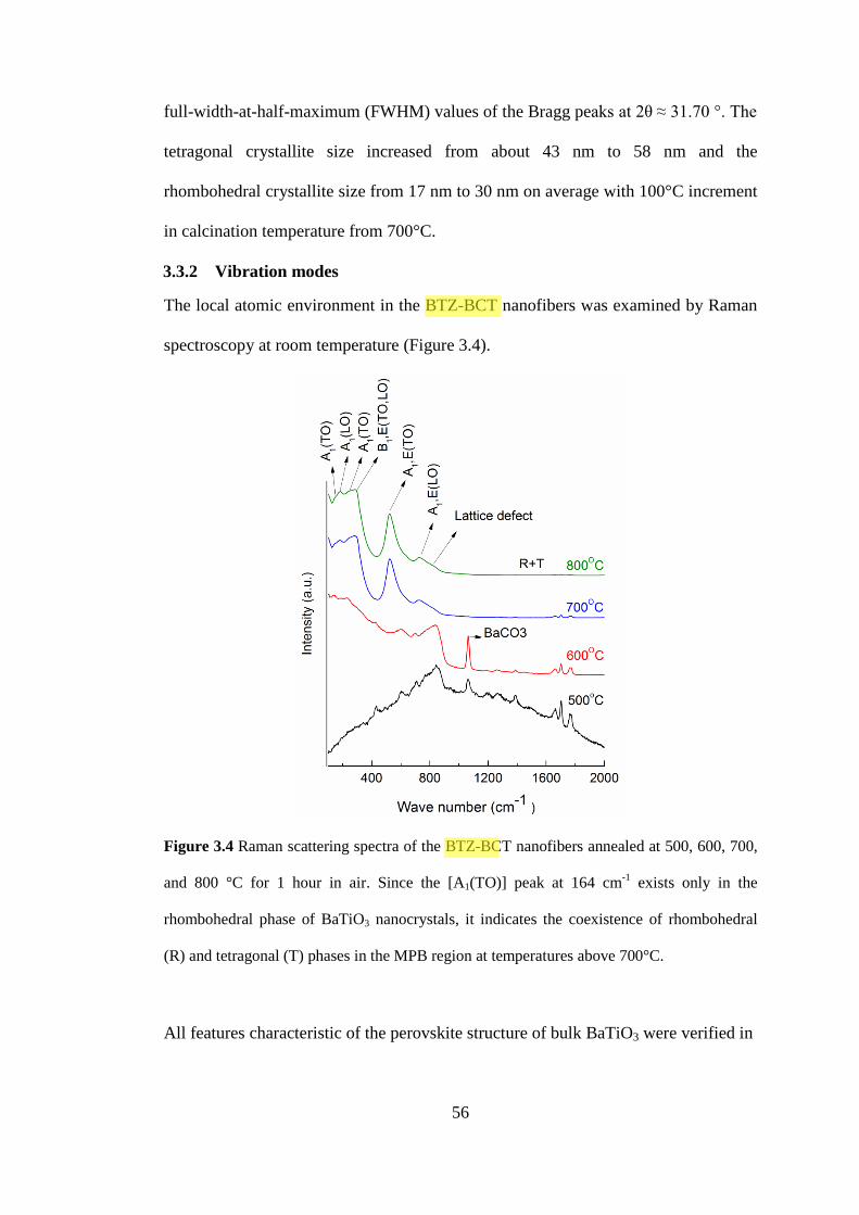
56
full-width-at-half-maximum (FWHM) values of the Bragg peaks at 2θ ≈ 31.70 °. The
tetragonal crystallite size increased from about 43 nm to 58 nm and the
rhombohedral crystallite size from 17 nm to 30 nm on average with 100°C increment
in calcination temperature from 700°C.
3.3.2 Vibration modes
The local atomic environment in the BTZ-BCT nanofibers was examined by Raman
spectroscopy at room temperature (Figure 3.4).
Figure 3.4 Raman scattering spectra of the BTZ-BCT nanofibers annealed at 500, 600, 700,
and 800 °C for 1 hour in air. Since the [A1(TO)] peak at 164 cm-1 exists only in the
rhombohedral phase of BaTiO3 nanocrystals, it indicates the coexistence of rhombohedral
(R) and tetragonal (T) phases in the MPB region at temperatures above 700°C.
All features characteristic of the perovskite structure of bulk BaTiO3 were verified in
aj393
Highlight
aj393
Highlight

57
the Raman spectra of bulk BTZ-BCT ceramics in different forms.[21, 22] Two A1
transverse optical modes [A1(TO)] and a longitudinal optical mode [A1(LO)],
together with a combined mode [B1,E(TO+LO)], are located in the range of 100 to
300 cm-1. Raman shifts at around 260 and 300 cm-1 are attributed to the Ti-O bond
vibrations. Ba-O bonds produce two mixed modes, [A1,E(TO)] and [A1,E(LO)], at
the high frequencies of about 520 and 725 cm-1. [21, 23] The A1 and E modes are
present in both Raman and infrared spectra, however, the B1 mode is only Raman
active. [21] The low intensity peak at 164 cm-1, assigned to the transverse optical
mode [A1(TO)], has been observed only in the rhombohedral phase of
nanocrystalline barium titanate, [24] while the other vibrational modes exist in both
tetragonal and rhombohedral phases. The coexistence of these two ferroelectric
phases in the Raman spectra confirms the crystallization of the BTZ-BCT nanofibers
and thin films in the MPB region.
Strain developed at the BTZ-BCT nanostructure-substrate interface together with the
substitution of Ca2+ and Zr4+, with ionic radii of 114 and 86 pm, respectively, for
Ba+2 and Ti+4 (with ionic radii of 146 pm and 74.5 pm, respectively) could be
responsible for the shift in the Raman spectra of BTZ-BCT bulks and nanofibers
compared to the polycrystalline BaTiO3. [22]
The signal appearing at 820 cm-1 could be generated by lattice defects caused by A or
B site vacancies in the ABO3 perovskite structure [25]. Three high frequency peaks in
the range of 1600 cm-1 to 1800 cm-1 are made faint by increasing the calcination
temperature up to 800 °C. The Raman revealed crystallization of the BTZ-BCT
nanofibers above 700 °C in coexisting tetragonal and rhombohedral symmetries is in
a good agreement with the XRD results and indicates the crystallization of the
nanofibers in the MPB region.
aj393
Highlight
aj393
Highlight

58
TEM studies were conducted for further investigation of the crystal structure and
phase content of the BTZ-BCT nanofibers. Regarding to crystallite sizes calculated
for tetragonal (43 nm) and rhombohedral phases (17 nm) at 700°C, large particles
correspond to the tetragonal phase, and small particles indicate rhombohedral phase
in Figure 3.5(a).
3.3.3 Crystalline phase observations by TEM
Figure 3.5 TEM results obtained from sample heat-treated at 700° C: (a) low magnification
image of a nanofibre containing larger tetragonal and smaller rhombohedral particles, with
inset selected area electron diffraction pattern; (b) indexing of the regions indicated in red
and green in (a) of {110} group reflections according to the indicated rhombohedral (R) and
tetragonal (T) phase reflections; (c) a second selected area diffraction pattern with
rhombohedral and tetragonal reflections as indicated; (d) high magnification image with
region containing fine twins indicated.

59
Analysis of the electron diffraction pattern acquired from the same fibre displayed in
Figure 3.5(a) shows that the nanofibers are composed of two crystalline structures,
tetragonal (T) and rhombohedral (R) (Figure 3.5(b) and(c)). Nanotwins about 10 nm
in length and 1-2 nm in width were observed in the high magnification image
displayed in Figure 3.5(d) as previously reported for BaTiO3 [26-28]. These twins could
be formed during the grain growth (growth twins) at high temperatures in the cubic
structure that is stable in ferroelectric phases, or they are generated by strain that
arises in the cubic-tetragonal or tetragonal-rhombohedral phase transitions
(deformation twins) below the Curie temperature. [29-31]. Twinning occurs to release
some of the elastic strains induced by the volume change that subsequently reduces
the total system energy. Lattice fringes near the twin boundaries show a symmetrical
mirror arrangement of the atoms in that area. Crystal defects such as twins, stacking
faults, and edge and screw dislocations act as pinning sites against the movement of
the ferroelectric domains and reduce their mobility. Suppression of the domain wall
mobility, either by the high density of grain boundaries due to the nanometer size
particles or crystal defects in the BTZ-BCT nanofibers reduces its piezoelectric
response [32, 33].
3.3.4 Piezoelectric and ferroelectric measurements by PFM
PFM was employed to quantify the piezoelectric coefficient in the BTZ-BCT fibers.
The deflection signal was calibrated by using the force-distance curve for the
cantilever (Figure 3.6) used for PFM measurements.
aj393
Highlight

60
Figure 3.6. Force-distance curve recorded from the surface of a silicon substrate using the
cantilever employed in our PFM measurements. This plot was used for the optical sensitivity
calibration of the cantilever.
Hysteretic bias voltage dependencies of the phase of the piezo-signal, the
displacement, and the piezoelectric coefficient in Figure 3.7(a)-(c) manifest the
switching of local ferroelectric domains in the BTZ-BCT thin film and nanofiber. A
DC-bias voltage, ranging from -5 V to +5 V, was employed. The PFM phase
hysteresis loops in Figure 3.7(a) show the 180° rotation of the electrical polarization
of domains in the BTZ-BCT nanofiber. Switching of polarization occurs due to an
inhomogeneous nucleation and anisotropic growth of domains [34] in external electric
field applied between the bottom electrode (Ir layer on Si wafer) and the top
electrode (PtIr-coated Si tip). The asymmetric shape of the hysteresis loops and their
shift toward the positive field (PtIr tip as anode) is due to the difference in work
functions, respectively, in the bottom and top electrodes: 4.23 eV for Ir and 5.6 eV
for PtIr. [35, 36]
aj393
Highlight

61
Figure 3.7 (a) Local PFM phase hysteresis loops and (b) piezoelectric butterfly loops of the
BTZ-BCT nanofiber obtained by switching the dc-bias voltage from -5 to +5 volts. 180°
domain switching in the phase hysteresis loop shows the switching of spontaneous electrical
dipoles built up in the BTZ-BCT fiber. (c) d33 hysteresis loop calculated by using the
converse piezoelectric equation, Δz = d33V, which indicates a significant enhancement of d33
= 180 pmV-1 in the BTZ-BCT nanofiber. (d) 3D topographic atomic force microscope
(AFM) image of the nanofiber used for the PFM measurements.
Figure 3.7(b) shows the displacement ∆z of the tip caused by the deformation of the
ferroelectric sample under applied electric field developed by the bias voltage.
Hysteretic curves exhibit an irreversible converse piezoelectric effect in BTZ-BCT
nanofiber. According to the definition of the converse piezoelectric effect, the
piezoelectric coefficient d33 can be calculated from the equation:
𝑑33 = ∆zV
(3.1) [37]
aj393
Highlight
aj393
Highlight

62
d33 values as high as 180 pmV-1 in fiber were obtained from the slope of the
linear part of the Δz vs. bias voltage curve at very low voltage.
The observed piezoelectric coefficient in our nanofibers exceeds that of all the
reported piezoelectric nanofibres, and comparable to the PZT ones. Table 3.1
compares the piezoelectric coefficient d33 of lead-containing and lead-free
piezoelectrics fabricated in the form of nanofibres.
Table 3.1 Comparison of the piezoelectric coefficient d33 of the BTZ-BCT nanofibres with
lead-based and lead-free piezoelectric nanofibres.
Materials Orientation d33(pm V-1) Ref.
BTZ-BCT Random 180 Current study
Pb(Zr0.3Ti0.7)O3 Random 83 [38]
0.65Pb(Mg1/3Nb2/3)O3–0.35PbTiO3 Random 50 [39]
CoFe2O4-Pb(Zr0.52Ti0.48)O3 Random 157 [40]
Bi3.4Ce0.6Ti3O12 Random 158 [41]
(Na0.82K0.18)0.5Bi0.5TiO3 Random 96 [42]
Bi3.15Nd0.85Ti3O12 Random 89 [43]
ZnO-V Random 121 [44]
(Na0.5Bi0.5)0.94TiO3-Ba0.06TiO3 Random 102 [42]
Their piezoelectric performances are comparable to d33 = 83-100 pm V-1 for PZT
nanofibers and thin films [38, 45] and considerably higher than those in Pb-free
piezoelectric materials such as (Na,K)NbO3 thin films with d33 = 40 pm V-1 [46] and
bismuth based layered ferroelectrics compositions in form of nanofibers and thin
films with d33 = 40-110 pm V-1 [43, 47]. Compared to PZT nanofibers, BaTiO3 thin
films, ZnO nanorods/pillars, and NaNbO3 nanowires exploited recently in high-
power piezoelectric generators [8, 48-51] (see Figure 3.8), our fibers seem to be capable
of significantly increased efficiency and output power in self-powered nanodevices
aj393
Highlight
aj393
Highlight

63
and energy harvesting systems. For example, according to Figure 3.8, d33 in BTZ-
BCT nanofibers exhibits more than 100% enhancement compared to the PZT
nanofibers. [38]
Figure 3.8 Comparison of piezoelectric coefficient d33 in nanostructured components used to
build piezoelectric generators with d33 in our BTZ-BCT films and fibers.
The reason for the high d33 values in our nanofibers is because the BTZ-BCT bulk
ceramics exhibit a very large piezoelectric effect compared to other piezoelectric
bulks. The large value (d33 = 1146 pm V-1) in the BTZ-BCT bulk ceramics is caused
by crystallization in the vicinity of the rhombohedral-cubic-tetragonal critical point
(critical triple point) which approaches the MPB region in the BTZ-BCT phase
diagram. The effects of the MPB and critical triple point on the piezoelectric
performance are discussed in details in Chapter 1. For this composition, the
polarization anisotropy vanishes, leading to a strong dependence of the electrical
polarization on elastic deformations, thus significantly increasing the
piezoelectricity. It is important to note that even a very small change in the
aj393
Highlight
aj393
Highlight

64
stoichiometry of the BTZ-BCT, as low as 5%, can result in drastic suppression of d33
in the final system of up to 40%.[20]
The equation (3.2) relates T (stress), E (electric field ), s13E (elastic compliance)
and d33 (inverse piezoelectric coefficient) to S (strain) in an unclamped piezoelectric
crystal.
𝑆3 = 𝑆13𝐸 (𝑇1 + 𝑇2) + 𝑆33𝐸 𝑇3 + 𝑑33𝐸3 (3.2) 40
It is well known that clamping to the substrate suppresses the strain and
consequently the measured converse piezoelectric coefficient in thin films and
nanofibers. The normal component of the electric field induces in-plane elastic stress,
σeffective. This affects normal deformations of the sample if a ferroelectric material is
tightly bonded with a rigid substrate. We assume the clamped nanofiber as the one-
dimensional object. Without applying stress on its free surfaces, T2=T3=0. The rigid
substrate can be considered as an isotropic object, therefore T1 =T in the nanofibers.
The T represents the effective stress.
Re-arranging the equation (3.2) with respect to the stress distributions in the
nanofibers, gives the effective piezoelectric coefficient 𝑑33,𝑓 for the one-dimensional
(equation (3.3)) objects.
𝑆3𝐸3
= 𝑑33,𝑓 = 𝑑33 + 𝑆13𝐸 σeffective𝐸3
(3.3)
Using d33 = 1140 pm V-1 [20] and s13E = 7.4 × 10⁻¹² m2 N-1 [52], experimentally obtained
in bulk BTZ-BCT ceramics, we present the effective piezoelectric coefficient 𝑑33,𝑓
and the effective stress σeffective calculated from equation (3.2) in Table 3.2.

65
Table 3.2 Calculated effective stress induced by electric field in the nanofiber-substrate
interface.
Geometry
Maximum 𝑑33,𝑓
(pm V-1)
EcA
(kV cm-1 )
𝑑33,𝑓
(pm V-1)a
σeffective
( MPa)
Nanofibre 180 20 151 284 a d33 measured in coercive field
3.3.5 Ferroelectric nanodomain imaging by SCM
Since electrical domains in ferroelectric materials manifest themselves as a local
distribution of surface charges, domain switching can be detected by the ac-field
scanning capacitance microscopy (SCM) technique. SCM is more ideal for
visualizing the ferroelectric domains in nanofibers with curved surfaces than PFM.
The topography of a single BTZ-BCT nanofiber (atomic force microscope (AFM)
image) and its SCM image obtained simultaneously are displayed in Figure 3.9(a)
and (b).
The sign and magnitude of the C-V slope in the SCM image is recorded and
converted to the dC/dV signals when the AC bias is applied to a local capacitor
constructed by the nanofiber and conductive tip, and the substrate, which function as
top and bottom electrodes, respectively. In order to record the differential
capacitance (dC/dV) image, a PtIr-coated Si tip was used. dC/dV signals were
achieved at small 1 V amplitude ac-bias between the tip and conducting substrate at
frequency of 90 kHz. The lock-in 180° phase mode was selected to observe the
opposite polarity of domains in the form of a contrast in the dC/dV images of
nanofibers.
aj393
Highlight

66
Figure 3.9 (a) Topographical (AFM), (b) SCM images, obtained in contact mode, of a single
BTZ-BCT nanofiber annealed at 700°C on a Si/SiO2/Ti/Ir conductive substrate. The two
distinct types of regions in black and white represent opposite out-of-plane electric domains,
averaging 24 nm in size and (c) schematic illustration of the SCM measurement. The sign
and magnitude of the C-V slope in the SCM image is recorded while the AC bias is applied
to a local capacitor constructed by the nanofiber and conductive tip, and the substrate as top
and bottom electrodes, respectively. The ferroelectric domain polarities and their
configurations are developed in the dC/dV image in the SCM as a result of different trends in
the dC/dV with respect to the polarization states.
Figure 3.9(b) shows the sharp contrast in a SCM image recorded simultaneously with
the topographical image of the same nanofiber in Figure 3.9 (a). Regarding the
schematic illustration of the SCM, measuring capacitance versus voltage and dC/dV
versus voltage in ferroelectric materials (see Figure 3.9(c)), while sweeping the
voltage from positive to negative, creates two distinct regions in the C-V plot. The
two peaks that exist in the C-V curve in the ferroelectric materials represent the
aj393
Highlight

67
spontaneous polarization switching. The ferroelectric domain polarities and their
configurations are developed in the dC/dV images in the SCM as a result of different
trends in the dC/dV with respect to the polarization states. Since in SCM imaging, the
dC/dV signal recorded from the surface is converted to a voltage output, which is
different from dC/dV, thus, the SCM image is scaled in volts, and ferroelectric
domains with the opposite polarizations create the sharp contrast in this image. Two
distinct types of region, displayed as black and white areas, were obtained in zero
volt dc-bias, which we interpret as opposite out-of-plane electric domains. They have
an average size of about 24 nm.
3.3.6 Electric resistance measurements by SSRM
2D resistivity of the BTZ-BCT nanofiber/substrate was studied using SPM operating
in the SSRM mode. A highly boron doped Si tip as the conductive tip scans in
contact mode over the nanofiber and substrate surface. In order to collect the
resistivity map of the BTZ-BCT nanofiber, a -5 V DC bias voltage was applied
between the tip and the sample. The resulting current passed through the fibre and
conductive layer of the substrate.
The topographic image (Figure 3.10(a)) and current distribution image (Figure
3.10(b)) of the nanofiber were recorded in real-time. The contrast revealed in the
SSRM image was induced by the difference in conductivity/resistivity of the
conductive layer of the substrate and the BTZ-BCT nanofiber. The bright area of the
SSRM image represents the conducting surface of the substrate, and the dark area
shows the high resistance BTZ-BCT nanofiber, which allows the current toflow
through by applying a -5 V DC-bias voltage. The uniform SSRM image reveals an
even current distribution in the nanofiber.
aj393
Highlight

68
Figure 3.10 (a) Topographical (AFM), (b) SSRM images, obtained in contact mode, of a
single BTZ-BCT nanofiber annealed at 700°C on a Si/SiO2/Ti/Ir conductive substrate. The
two distinct types of regions in dark and bright colours represent the current distribution in
the conducting substrate and ferroelectric nanofiber. (c) Section analysis of the SSRM
image, and (d) reference transfer curve of the SSRM logarithmic current amplifier in
different biases.
This develops a highly homogeneous electric field distribution when a voltage is
employed on the fiber and impedes the non-uniform development of stresses/strains
in the nanofibers. These homogeneities in the current, electric field, and
consequently, the stress/strain distribution result in more accuracy in displacement,
higher output voltage, and longer lifetime of a device based on the BTZ-BCT
nanofibers. A section analysis of the SSRM image is shown in Figure 3.10(c).
According to the reference transfer curve of the SSRM logarithmic current amplifier
(Figure 3.10(d)) and the maximum output voltage extracted from the section
aj393
Highlight
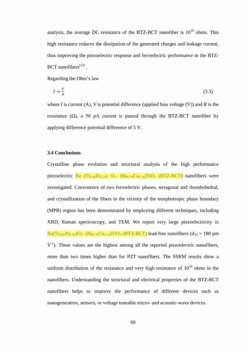
69
analysis, the average DC resistance of the BTZ-BCT nanofiber is 1010 ohms. This
high resistance reduces the dissipation of the generated charges and leakage current,
thus improving the piezoelectric response and ferroelectric performance in the BTZ-
BCT nanofibers[15] .
Regarding the Ohm’s law
𝐼 = 𝑉𝑅 (3.3)
where I is current (A), V is potential difference (applied bias voltage (V)) and R is the
resistance (Ω), a 50 pA current is passed through the BTZ-BCT nanofiber by
applying difference potential difference of 5 V.
3.4 Conclusions
Crystalline phase evolution and structural analysis of the high performance
piezoelectric Ba (Ti0.80Zr0.20) O3- (Ba0.70Ca0.30)TiO3 (BTZ-BCT) nanofibers were
investigated. Coexistence of two ferroelectric phases, tetragonal and rhombohedral,
and crystallization of the fibers in the vicinity of the morphotropic phase boundary
(MPB) region has been demonstrated by employing different techniques, including
XRD, Raman spectroscopy, and TEM. We report very large piezoelectricity in
Ba(Ti0.80Zr0.20)O3- (Ba0.70Ca0.30)TiO3 (BTZ-BCT) lead-free nanofibers (d33 = 180 pm
V-1). These values are the highest among all the reported piezoelectric nanofibers,
more than two times higher than for PZT nanofibers. The SSRM results show a
uniform distribution of the resistance and very high resistance of 1010 ohms in the
nanofibers. Understanding the structural and electrical properties of the BTZ-BCT
nanofibers helps to improve the performance of different devices such as
nanogenerators, sensors, or voltage tuneable micro- and acoustic-wave devices.
aj393
Highlight
aj393
Highlight

70
3.5 References
[1] A. Bernal, A. Tselev, S. Kalinin, N. Bassiri-Gharb, Adv. Mater. 2012, 24,
1159.
[2] P. M. Rørvik, T. Grande, M.-A. Einarsrud, Adv. Mater. 2011, 23, 4007.
[3] B. J. Hansen, Y. Liu, R. Yang, Z. L. Wang, ACS Nano 2010, 4, 3647.
[4] Y. Bourquin, R. Wilson, Y. Zhang, J. Reboud, J. M. Cooper, Adv. Mater.
2011, 23, 1458.
[5] A. Jalalian, A. M. Grishin, Appl. Phys. Lett. 2012, 100, 012904.
[6] S. V. Kalinin, N. Setter, A. L. Kholkin, MRS Bull. 2009, 34, 634.
[7] Z. L. Wang, Adv. Funct. Mater. 2008, 18, 3553.
[8] X. Chen, S. Xu, N. Yao, Y. Shi, Nano Lett. 2010, 10, 2133.
[9] J. Chang, M. Dommer, C. Chang, L. Lin, Nano Energy 2012, 1, 356.
[10] P. Eyben, F. Seidel, T. Hantschel, A. Schulze, A. Lorenz, A. U. De Castro, D.
Van Gestel, J. John, J. Horzel, W. Vandervorst, physica status solidi (a) 2011, 208,
596.
[11] X. Ou, P. D. Kanungo, R. Kögler, P. Werner, U. Gösele, W. Skorupa, X.
Wang, Nano Lett. 2009, 10, 171.
[12] Y. Kim, C. Bae, K. Ryu, H. Ko, Y. K. Kim, S. Hong, H. Shin, Appl. Phys.
Lett. 2009, 94, 032907.
[13] J. Y. Son, S. H. Bang, J. H. Cho, Appl. Phys. Lett. 2003, 82, 3505.
[14] L. Y. Kraya, R. Kraya, J. Appl. Phys. 2012, 111, 013708.
[15] D. A. Scrymgeour, J. W. P. Hsu, Nano Lett. 2008, 8, 2204.
[16] K. Fujihara, A. Kumar, R. Jose, S. Ramakrishna, S. Uchida, Nanotechnology
2007, 18, 365709.
[17] A. Shui, L. Zeng, K. Uematsu, Scripta Mater. 2006, 55, 831.

71
[18] Y. Li, Y. Qian, H. Liao, Y. Ding, L. Yang, C. Xu, F. Li, G. Zhou, Science
1998, 281, 246.
[19] J. T. McCann, J. I. L. Chen, D. Li, Z.-G. Ye, Y. Xia, Chem. Phys. Lett. 2006,
424, 162.
[20] W. Liu, X. Ren, Phys. Rev. Lett. 2009, 103, 257602.
[21] U. D. Venkateswaran, V. M. Naik, R. Naik, Phys. Rev. B 1998, 58, 14256.
[22] Y. Shiratori, C. Pithan, J. Dornseiffer, R. Waser, J. Raman Spectrosc. 2007,
38, 1300.
[23] M. C. Chang, S.-C. Yu, J. Mater. Sci. Lett. 2000, 19, 1323.
[24] C. J. Xiao, C. Q. Jin, X. H. Wang, Mater. Chem. Phys. 2008, 111, 209.
[25] Y. Shiratori, C. Pithan, J. Dornseiffer, R. Waser, J. Raman Spectrosc. 2007,
38, 1288.
[26] E. Hamada, W.-S. Cho, K. Takayanagi, Philos. Mag. A 1998, 77, 1301.
[27] M. Fujimoto, J. Cryst. Growth 2002, 237–239, Part 1, 430.
[28] H. Oppolzer, H. Schmelz, J. Am. Ceram. Soc. 1983, 66, 444.
[29] W. Cao, L. E. Cross, Phys. Rev. B 1991, 44, 5.
[30] B.-K. Lee, S.-J. L. L. Kang, Acta Mater. 2001, 49, 1373.
[31] M. Daraktchiev, R. J. Harrison, E. H. Mountstevens, S. A. T. Redfern,
Materials Science and Engineering: A 2006, 442, 199.
[32] A. Gruverman, A. Kholkin, Rep. Prog. Phys. 2006, 69, 2443.
[33] L. Sagalowicz, F. Chu, P. D. Martin, D. Damjanovic, J. Appl. Phys. 2000, 88,
7258.
[34] C. T. Nelson, P. Gao, J. R. Jokisaari, C. Heikes, C. Adamo, A. Melville, S.-H.
Baek, C. M. Folkman, B. Winchester, Y. Gu, Y. Liu, K. Zhang, E. Wang, J. Li, L.-Q.
Chen, C.-B. Eom, D. G. Schlom, X. Pan, Science 2011, 334, 968.

72
[35] S. Brimley, M. S. Miller, M. J. Hagmann, J. Appl. Phys. 2011, 109, 094510.
[36] Z. Li, J. A. Bain, Z. Jian-Gang, L. Abelmann, T. Onoue, IEEE Transactions
on Magnetics 2004, 40, 2549.
[37] A. L. Kholkin, C. Wutchrich, D. V. Taylor, N. Setter, Rev. Sci. Instrum. 1996,
67, 1935.
[38] M. Fan, W. Hui, Z. Li, Z. Shen, H. Li, A. Jiang, Y. Chen, R. Liu,
Microelectron. Eng. 2012, 98, 371.
[39] S. Xu, G. Poirier, N. Yao, Nano Energy 2012, 1, 602.
[40] S. H. Xie, J. Y. Li, Y. Qiao, Y. Y. Liu, L. N. Lan, Y. C. Zhou, S. T. Tan,
Appl. Phys. Lett. 2008, 92, 062901.
[41] B. Jiang, M. Tang, J. Li, Y. Xiao, H. Tao, Y. Zhou, J. He, J. Electron. Mater.
2012, 41, 651.
[42] Y. Q. Chen, X. J. Zheng, X. Feng, S. H. Dai, D. Z. Zhang, Mater. Res. Bull.
2010, 45, 717.
[43] M. Liao, X. L. Zhong, J. B. Wang, S. H. Xie, Y. C. Zhou, Appl. Phys. Lett.
2010, 96, 012904.
[44] Y. Q. Chen, X. J. Zheng, X. Feng, Nanotechnology 2010, 21, 055708.
[45] D. V. Taylor, D. Damjanovic, Appl. Phys. Lett. 2000, 76, 1615.
[46] C. W. Ahn, S. Y. Lee, H. J. Lee, A. Ullah, J. S. Bae, E. D. Jeong, J. S. Choi,
B. H. Park, I. W. Kim, J. Phys. D: Appl. Phys. 2009, 42, 215304.
[47] S. Fujino, M. Murakami, V. Anbusathaiah, S. H. Lim, V. Nagarajan, C. J.
Fennie, M. Wuttig, L. Salamanca-Riba, I. Takeuchi, Appl. Phys. Lett. 2008, 92,
202904.
[48] K.-I. Park, M. Lee, Y. Liu, S. Moon, G.-T. Hwang, G. Zhu, J. E. Kim, S. O.
Kim, D. K. Kim, Z. L. Wang, K. J. Lee, Adv. Mater. 2012, 24, 2999.

73
[49] K.-I. Park, S. Xu, Y. Liu, G.-T. Hwang, S.-J. L. Kang, Z. L. Wang, K. J. Lee,
Nano Lett. 2010, 10, 4939.
[50] Y. Hu, Y. Zhang, C. Xu, G. Zhu, Z. L. Wang, Nano Lett. 2010, 10, 5025.
[51] J. H. Jung, M. Lee, J.-I. Hong, Y. Ding, C.-Y. Chen, L.-J. Chou, Z. L. Wang,
ACS Nano 2011, 5, 10041.
[52] D. Xue, Y. Zhou, H. Bao, C. Zhou, J. Gao, X. Ren, J. Appl. Phys. 2011, 109,
054110.

74
Chapter 4. BTZ-BCT Thin Films
In this Chapter, the synthesis and characterization of Ba(Ti0.80Zr0.20)O3-
(Ba0.70Ca0.30)TiO3 (BTZ-BCT) thin films will be presented. Crystalline phase content
and topography of the films will be examined. Ferroelectric domain configuration,
and piezoelectric and ferroelectric properties of the thin films will be investigated
using different techniques, including piezoelectric force microscopy (PFM) and
polarization versus electric field hysteresis loops.
4.1 Introduction
Integration of high performance piezoelectrics in piezoelectric devices and micro-
/nano-electromechanical systems (MEMS, NEMS) is a viable approach to enhance
their efficiency. Low-dimensional piezoelectric and ferroelectric materials have been
exploited widely in nanogenerators, sensors, transducers, MEMS devices, and other
applications, such as microwave varactors and ferroelectric field effect transistors.[1-6]
For instance, high performance piezoelectric nanostructures can enhance the output
power of piezoelectric generators that convert the kinetic energy of vibrations,
displacements, or applied force to electricity.[7-11]
In this study, observations on the high piezoelectric response achieved in BTZ-BCT
thin films are reported, along with visualization of ferroelectric nanodomains with
high spatial resolution using PFM. The influences of lateral size, geometry, and the
clamping effect on the piezoelectric performance were also investigated for thin
films and compared with BTZ-BCT nanofibers.
aj393
Highlight
aj393
Highlight

75
4.2 Experimental procedure
Ba(Ti0.80Zr0.20)O3- (Ba0.70Ca0.30)TiO3 thin film was fabricated using the spin-coating
technique. In order to prepare the BTZ-BCT precursor solution, barium acetate,
calcium acetate monohydrate, titanium butoxide, and zirconium (IV) propoxide were
used as starting materials. Barium acetate and calcium acetate monohydrate were
dissolved in glacial acetic acid at 80°C for 1 hour and cooled down to room
temperature. Titanium butoxide and zirconium propoxide were chelated by acetyl
acetone and added to the Ba and Ca solution. 2-methoxyethanol was used to adjust
the concentration of the BTZ-BCT precursor solution to 0.2 M. Spin-coating at 3000
rpm for 30 seconds was carried out to prepare the BTZ-BCT thin film on Si and
Si/SiO2/Ti/Ir substrates. The spin-coated thin films were dried and annealed at 100°C
and 600°C for 10 minutes, respectively, and the above procedure was repeated for 4
cycles until the films reached a thickness of about 200 nm, followed by calcination at
700°C for 1 hour in air.
Field-emission scanning electron microscopy (FE-SEM, JEOL JSM 7500FA) was
used to examine the surface morphology and microstructure of the cross-section of
the thin film with a 3.8 mm working distance under 1 kV acceleration voltage. A
Raman spectrometer (HORIBA JobinYvon, HR800 spectrometer) was employed to
study the state of crystallization and lattice vibration modes. Un-polarized spectra
were collected at room temperature using 632.8 nm light pumping from a He-Ne
laser and a charge coupled device (CCD) detector in this experiment.
Piezoresponse force microscopy (PFM, Asylum Research, MFP-3D) and scanning
capacitance microscopy (Digital Instrument, Dimension 3100) were used for our
experiments. Our PFM measurements were performed at a low frequency of 10 Hz
aj393
Highlight
aj393
Highlight

76
and in electric field, ranging from -300 kV/cm to +300 kV/cm. The bottom electrode
was an Ir layer on Si wafer and the top electrode was a PtIr-coated Si tip with
deflection sensitivity of 73.6 nm V-1 for our experiments, respectively.
4.3 Results and discussion
4.3.1 Morphology studies using FE-SEM and AFM
Figure 4.1 (a) FE-SEM image of BTZ-BCT thin film deposited on the Si/SiO2/Ti/Ir
substrate and annealed at 700°C for 1 hour in air. Inset: magnified view of the thin film
surface. (b) FE-SEM image of cross-section of BTZ-BCT thin film about 200 nm in
thickness with an average particle size of 33 nm. (c) 3D AFM image of topography of BTZ-
BCT thin film annealed at 700°C for 1 hour, showing 2 nm rms surface roughness.
(a) (b)
(c)
aj393
Highlight
aj393
Highlight

77
Field emission scanning electron microscope (FE-SEM) images from the surface and
cross-section of the BTZ-BCT thin film are displayed in Figures 4.1(a) and (b). The
image of the 200 nm thick BTZ-BCT film in Figure 4.1(b) reveals randomly oriented
particles. The images were collected at 3.8 mm working distance under 1 kV
acceleration voltage.
A typical three-dimensional (3D) atomic force microscope (AFM) image of a 400 ×
400 nm2 surface area of a BTZ-BCT thin film spin-coated on Si/SiO2/Ti/Ir substrate
and heat-treated at 700°C for 1 hour is shown in Figure 4.1(c).
The films have a smooth surface with a surface root mean square (rms) roughness
equal to 2.1 nm, with an average particle size of 33 nm.
4.3.2 Phase content investigation using XRD and Raman spectroscopy
The X-ray diffraction pattern of the thin film annealed at 700°C is presented in
Figure 4.2(a). The Bragg reflections demonstrate no preferred directional growth in
the film, which is similar to the case of the BTZ-BCT nanofibers that were annealed
under the same conditions using the same precursor solution.
Local atomic environments in the BTZ-BCT films were examined by Raman
spectroscopy at room temperature. A typical spectrum is displayed in Figure 4.2(b).
All features characteristic of the perovskite structure of bulk BaTiO3 were verified in
the Raman spectra of the thin film and are in good agreement with the results for the
other BTZ-BCT counterparts, which were analyzed in previous chapters in detail [12,
13].
aj393
Highlight
aj393
Highlight

78
Figure 4.2 (a) X-ray diffraction pattern of the BTZ-BCT thin film annealed at 700°C on the
Si substrate. (b) Raman spectrum of BTZ-BCT 200 nm thick BTZ-BCT film spin-coated on
Si/SiO2/Ti/Ir substrate annealed at 700°C for 1 hour in air. The spectrum of the substrate
alone is included for reference. All features are characteristic of the polar structure of
BaTiO3 and indicate successful evolution of the perovskite structure in all samples. The
existence of a peak at 164 cm-1 [A1(TO)] is only observed in the rhombohedral symmetry,
while the other peaks, which appear in both tetragonal and rhombohedral symmetries,
indicate the crystallization in morphotropic phase boundary (MPB) region.
The transverse optical mode [A1(TO)] located at 164 cm-1 is recorded in higher
intensity compared to the nanofibers. This peak has been observed only in the
rhombohedral phase of nanocrystalline barium titanate [14], while the other
vibrational modes exist in both tetragonal and rhombohedral phases. The coexistence
of these two ferroelectric phases in the Raman spectra confirms the crystallization of
the BTZ-BCT thin films in the MPB region.
4.3.3 Piezoelectric and ferroelectric properties investigation by PFM
Figure 4.3(a) and (b) presents 3D- PFM patterns of the surface of a 200 nm thick
BTZ-BCT film. Simultaneous recording of 3D profiles of the PFM phase and
amplitude signals enables a visualization of ferroelectric domains. These 3D images
(a) (b)

79
were acquired using a lock-in amplification technique with a PtIr-coated silicon
cantilever in contact mode, which was ac-biased with a voltage of 1.0 V.
Figure 4.3 3D PFM phase (a) and amplitude (b) images of the surface of 200 nm thick BTZ-
BCT film. Ferroelectric domain patterns in the phase image (a) display the opposite polarity
of ferroelectric domains 20 to 40 nm in size. These domains are revealed by 180° phase
difference contrast. The amplitude image (b) reproduces the domain shape. Sharp contrast
around domains visualizes domain boundaries. In (c), phase and amplitude profiles recorded
along the marked lines in (a) and (b) are overlaid on an AFM topographical image. All three
images were collected simultaneously under 1.0 V ac modulation voltage.
Ferroelectric domains have a lateral size of 20 to 40 nm. 180° PFM phase contrast in
Figure 4.3(a) distinctly shows that ferroelectric domains have antiparallel out-of-
plane polarization. The PFM amplitude pattern in Figure 4.3(b) reproduces the shape
(a)
(b)
(c)

80
of the domains. In Figure 4.3(c), phase and amplitude cross-sectional profiles
recorded along the marked line are overlaid on the topographical image taken from
Figure 4.4 (a) Local PFM phase hysteresis loops and (b) piezoelectric butterfly loops of the
BTZ-BCT thin film obtained by switching the bias voltage from -5 to +5 volts (±300 kV cm-
1 electric field). 180° domain switching in the phase hysteresis loop shows the switching
phenomenon of spontaneous electrical dipoles built up in the BTZ-BCT thin film. (c) d33
hysteresis loop calculated by using the converse piezoelectric equation, Δz = d33V, which
indicates the piezoelectric coefficient d33 = 141 pmV-1 in the BTZ-BCT thin film. (d)
Schematic illustration of lateral size and contact area in the thin film and nanofiber.
Figure 4.1(c). Sharp 180° PFM phase contrast occurs when the conducting cantilever
crosses narrow domain boundaries.
PFM was employed to quantify the piezoelectric coefficient in the BTZ-BCT films
under the same operational parameters used for the nanofibers. Figure 4.4(a) and (b)
aj393
Highlight

81
demonstrates the ferroelectric domain switching and displacement of the thin film
respectively developed via the inverse piezoelectric effect. It should be noted that the
PFM signals were calibrated using a force-distance curve before each measurement.
The calculated piezoelectric coefficient in the BTZ-BCT thin films (Figure 4.4(c))
shows smaller value compare to the nanofibers. We explain this by the much smaller
lateral size of the fiber-substrate interface and the fiber-to-substrate contact area, as
shown in Figure 4.4(d). Reduction of the residual ferroelectric-substrate interface
strain increases the piezoelectric response in the nanofibers.
Table 4.1 Comparison of the piezoelectric coefficient d33 in some Pb-based and Pb-
free piezoelectric thin films.
Materials Orientation d33
(pm V-1) Ref.
BTZ-BCT Random 141 Current
study
BaTiO3 (100) 30 [15]
BaTiO3 Single crystal 80-100 [16]
Pb0.76Ca0.24TiO3 Random 70 [17]
Bi0.83Sm0.17FeO3 (002) 110 [18]
BiFeO3 (001) 70 [19]
0.34BiScO3-0.66PbTiO3 (001) 130 [20]
0.948(K0.5Na0.5)NbO3–0.052LiSbO3 Random 50 [21]
(K0.44,Na0.52,Li0.04)(Nb0.84,Ta0.1,Sb0.06)O3 (001) 53 [22]
Pb(Zr0.6Ti0.4)O3
(100) 100 [23] (111) 63
Random 77
0.7Pb(Mg1/3Nb2/3)O3–0.3PbTiO3
(111)
79 [24] 0.9Pb(Mg1/3Nb2/3)O3–0.1PbTiO3 64
Pb(Zr0.6Ti0.4)O3 85
(K0.5Na0.5)NbO3 with 20 mol% extra K and Na. Random 40 [25]
aj393
Highlight

82
Similar to the BTZ-BCT nanofibers, the observed piezoelectric coefficients in our
thin film is exceeding those of lead zirconate titanate (PZT). Table 4.1 compares the
piezoelectric coefficient d33 for lead-containing and lead-free piezoelectric thin films
with textured and random crystal structures. According to Table 4.1, d33 in BTZ-BCT
thin films exhibits more than 100% enhancement compared to the PZT thin films
with a random orientation structure [25].
Since the same precursor solution as for the nanofibers was used for the thin films,
and the same crystal structure and phase content were developed as for the
nanofibers, crystallization in the vicinity of the MPB suppresses the free energy
barrier against the polarization rotation from rhombohedral to tetragonal and vice
versa. Reducing the energy barrier and eliminating the polarization anisotropy
enhanced the piezoelectric performance in the BTZ-BCT constrained structures,
including the thin films.
Table 4.2 Calculated effective stress induced by electric field in the thin film −
substrate interface.
Geometry Maximum𝑑33,𝑓
(pm V-1)
EcA
(kV cm-1 )
𝑑33,𝑓
(pm V-1)a
σeffective
( MPa)
Thin film 141 45 122 302.7 a d33 measured in coercive field
Suppression of the piezoelectric coefficient in the thin films compared to the BTZ-
BCT ceramics occurs because of the same reason as for the other constrained
structures such as nanofibers, as discussed in Chapter 3. We assume the clamped thin
films as the two-dimensional objects. Without applying stress on their free surfaces,
aj393
Highlight

83
T3=0 for the the thin films, therefore T1=T2=T. The T represents the effective stress.
The equation (4.1) gives the effective piezoelectric coefficient 𝑑33,𝑓 for the one-
dimensional objects.
𝑆3𝐸3
= 𝑑33,𝑓 = 𝑑33 + 2𝑆13𝐸 σeffective𝐸3
(4.1)
The calculated effective stress (σeffective) in the thin film ─ substrate interface is listed
in Table 4.2.
Figure 4.5 Polarization versus electric field (P-E) loop obtained at 1 kHz of the BTZ-BCT
thin film with about 200 nm thickness deposited on the Si/SiO2/Ti/Ir substrate.
The polarization versus electric field loop is displayed in Figure 4.5. The
ferroelectric hysteresis loop was recorded at 1 kHz. The ferroelectric domain
switching was saturated under an average electric field of Ec = 45.8 kV cm-1 and
achieved maximum polarization Ps = 6.9 µC cm-1, and remanent polarization Pr = 2.4
aj393
Highlight

84
µC cm-1 in the BTZ-BCT thin film with about 200nm thickness deposited on the
Si/SiO2/Ti/Ir substrate.
4.4 Conclusions
In conclusion, we report very large piezoelectricity in Ba(Ti0.80Zr0.20)O3-
(Ba0.70Ca0.30)TiO3 (BTZ-BCT) lead-free thin films with piezoelectric coefficient d33
= 141 pm V-1 . This value is the highest among all the reported piezoelectric thin
films, about two times higher than for PZT films with randomly oriented structure.
4.5 References
[1] Z. L. Wang, J. Song, Science 2006, 312, 242.
[2] M. Bhaskaran, S. Sriram, S. Ruffell, A. Mitchell, Adv. Funct. Mater. 2011,
21, 2251.
[3] S. C. Masmanidis, R. B. Karabalin, I. De Vlaminck, G. Borghs, M. R.
Freeman, M. L. Roukes, Science 2007, 317, 780.
[4] P. Muralt, J. Micromech. Microeng. 2000, 10, 136.
[5] C.-R. Cho, J.-H. Koh, A. Grishin, S. Abadei, S. Gevorgian, Appl. Phys. Lett.
2000, 76, 1761.
[6] S.-M. Koo, S. Khartsev, C.-M. Zetterling, A. Grishin, M. Ostling, Appl. Phys.
Lett. 2003, 83, 3975.
[7] K.-I. Park, M. Lee, Y. Liu, S. Moon, G.-T. Hwang, G. Zhu, J. E. Kim, S. O.
Kim, D. K. Kim, Z. L. Wang, K. J. Lee, Adv. Mater. 2012, 24, 2999.
[8] X. Chen, S. Xu, N. Yao, Y. Shi, Nano Lett. 2010, 10, 2133.
[9] Y. Hu, Y. Zhang, C. Xu, G. Zhu, Z. L. Wang, Nano Lett. 2010, 10, 5025.
aj393
Highlight
aj393
Highlight
aj393
Highlight

85
[10] H. D. Espinosa, R. A. Bernal, M. Minary-Jolandan, Adv. Mater. 2012, 24,
4656.
[11] B. J. Hansen, Y. Liu, R. Yang, Z. L. Wang, ACS Nano 2010, 4, 3647.
[12] U. D. Venkateswaran, V. M. Naik, R. Naik, Phys. Rev. B 1998, 58, 14256.
[13] Y. Shiratori, C. Pithan, J. Dornseiffer, R. Waser, J. Raman Spectrosc. 2007,
38, 1300.
[14] C. J. Xiao, C. Q. Jin, X. H. Wang, Mater. Chem. Phys. 2008, 111, 209.
[15] Y. Guo, K. Suzuki, K. Nishizawa, T. Miki, K. Kato, J. Cryst. Growth 2005,
284, 190.
[16] Y.-B. Park, J. L. Ruglovsky, H. A. Atwater, Appl. Phys. Lett. 2004, 85, 455.
[17] A. L. Kholkin, M. L. Calzada, P. Ramos, J. Mendiola, N. Setter, Appl. Phys.
Lett. 1996, 69, 3602.
[18] S. Fujino, M. Murakami, V. Anbusathaiah, S. H. Lim, V. Nagarajan, C. J.
Fennie, M. Wuttig, L. Salamanca-Riba, I. Takeuchi, Appl. Phys. Lett. 2008, 92,
202904.
[19] J. Wang, J. B. Neaton, H. Zheng, V. Nagarajan, S. B. Ogale, B. Liu, D.
Viehland, V. Vaithyanathan, D. G. Schlom, U. V. Waghmare, N. A. Spaldin, K. M.
Rabe, M. Wuttig, R. Ramesh, Science 2003, 299, 1719.
[20] H. Wen, X. Wang, C. Zhong, L. Shu, L. Li, Appl. Phys. Lett. 2007, 90,
202902.
[21] J. Ryu, J.-J. Choi, B.-D. Hahn, D.-S. Park, W.-H. Yoon, Appl. Phys. Lett.
2008, 92, 012905.
[22] M. Abazari, T. Choi, S. W. Cheong, A. Safari, J. Phys. D: Appl. Phys. 2010,
43, 025405.
[23] D. V. Taylor, D. Damjanovic, Appl. Phys. Lett. 2000, 76, 1615.

86
[24] R. Herdier, M. Detalle, D. Jenkins, C. Soyer, D. Remiens, Sensor. Actuat. A:
Phys. 2008, 148, 122.
[25] C. W. Ahn, S. Y. Lee, H. J. Lee, A. Ullah, J. S. Bae, E. D. Jeong, J. S. Choi,
B. H. Park, I. W. Kim, J. Phys. D: Appl. Phys. 2009, 42, 215304.

87
Chapter 5. Biocompatible Piezoelectric Nanofibers
In this chapter, piezoelectric properties and ferroelectric nano-domains developed in
the NKN nanofibers are investigated.
Biocompatible and piezoelectric (Na,K)NbO3 (NKN) nanofibers are synthesized by
sol-gel assisted electrospinning technique. X-ray diffraction pattern of the nanofibers
reveals a pure and single phase of polar structure after annealing at 700°C.
Transmission electron microscope images and electron diffraction pattern show the
growth of NKN single crystals in the form of nanofibers. The ferroelectric domain
switching and piezoelectric response of the nanofibers are investigated using
piezoelectric force microscopy (PFM) technique. A significantly higher piezoelectric
response is achieved in NKN nanofibers compare to its thin films. Owing
permanently charged regions in the NKN nanofibers known as ferroelectric domains
and generating the electrical signals via piezoelectric effect in them provide a new
opportunity for construction of a smart biocompatible scaffold which can be used for
repair, engineering and regeneration of damaged tissues.
5.1 Introduction
Electrically active materials have been approved to accelerate tissue growth and
improve the adaptation of the surrounding tissue of an implant or damaged tissues [1-
4]. Surface charges could be generated either in ionic biomaterials (e.g.
hydroxyapatite (HA)) due to the cation and anion separation in opposite orientations
under an electric field or as a result of piezoelectricity in piezoelectric materials such
as quartz that surface charges are created on the crystal surfaces under appropriate

88
mechanical stress. Possessing permanently charged regions in ferroelectric materials
(a subgroup of the piezoelectrics) known as ferroelectric domains and generating the
electrical signals via piezoelectric effect, have attracted intensive interest to exploit
them in biological applications [3, 5]. Electrical signals generated on the surface of
these materials stimulate nerves resulted in an enhanced blood flow in tissues[1]. In
terms of bone in growth, surface charges created on the implant surface, enhance the
protein adsorption onto the implant surface which leads to improve the
osteoconduction on the implant surfaces compare to neutral surfaces[6]. Beloti et al
demonstrated that the attachment of the human osteoblatic cells to the implants was
noticeably promoted in piezoelectric implants consists of P(VDF-TrFE)/BaTiO3
composite compare to the non-piezoelectric compounds [3]. Piezoelectric materials
can imitate the bone reaction [7, 8] when a force is applied and produce electrical
charges. There have been several reports that confirm piezoelectric phenomenon
improves the bone tissue growth and biological response [9-11].
Hydroxapatite Ca10(PO4)6(OH)2 has a composition similar to the natural bone (
Calcium phosphate) and excellent biocompatibility, however lack of permanent
charged regions and naturally neutral surfaces states further demand for new
compositions and structures[12]. There have been several efforts to merge
piezoelectricity with biocompatibility in composite and complex structures such as
HA- BaTiO3, polyvinylideneflouride (PVDF) - HA and PVDF-(Pb(Zr0.53Ti0.47)O3) [5,
13, 14]. In most cases addition of piezoelectric materials to the bioceramics only
increased the dielectric constant and did not show an improvement in the
piezoelectric performance due to the non-continues structure in piezoelectric segment
or limited their application due to the toxicity of additional part.

89
Nilsson et al Patented piezoelectric (Na, K) NbO3 ceramics (NKN) as a
biocompatible piezoelectric material for medical implants [15]. According to
toxicology examination, NKN mentioned excellent biocompatibility and acceptable
durability in form of ceramics and thin films. This invention inspired us to design
and fabricate a 3D structure constructed with NKN nanofibers which can be
employed as a scaffold for stimulation and encouraging the tissue growth.
In this paper, piezoelectric properties and ferroelectric nano-domains developed in
the NKN nanofibers are investigated.
5.2 Experimental procedure (Na, K)NbO3 precursor solution was prepared via sol-gel method. Potassium acetate
and sodium acetate were mixed in 2-methoxyethanol at room temperature and stirred
for 1 hour followed by adding a niobium ethoxide solution dissolved in acetyl
acetone. Polyvinylpyrrolidone (PVP, 0.035 g ml-1) as a binder was added to the NKN
sol to prepare the solution for electrospinning. The solution was transferred to a
plastic syringe with a metallic needle. Electrospinning was carried at 1.8 kVcm-1
electric field strength between the metallic needle and aluminium foil collector
located 8cm below the needle. A non-woven and bead-free nanofibers mat was
collected from the surface of the collector after drying at 100 °C in nitrogen
atmosphere for 12 hours followed by annealing at 600, 700 and 800°C for 1 hour in
air. Heating/cooling rate was 5 °C min-1.
Crystal structure evolution of the nanofibers calcined at different temperatures was
studied by X-ray diffraction (GBC MMA powder diffractometer, CuKα radiation, 40
kV, 25 mA). Raman spectra were collected (HORIBA jobin yvon, HR800
spectrometer) at room temperature in air by pumping samples with 632.8 nm He-Ne

90
laser light. Field emission scanning electron microscope (FE-SEM, JEOL JSM
7500FA) was used to collect images of nanofibers. Transmission electron
microscopy (TEM) was performed using a JEOL 2011 200 KeV analytical
instrument. Samples were prepared by dispersion onto “Quantifoil” holey carbon
support film with examination of sample regions located over holes in the support
film.
Piezoresponse force microscopy (PFM, Asylum Research, MFP-3D) for
piezoelectric properties measurements was used. A PtIr-coated Si tip for the PFM
was employed. Bottom electrode is Ir layer on Si wafer and the top electrode is the
conducting tip.
5.3 Results and discussions
5.3.1 Morphology and Crystalline phase evolution
Figure 5. 1 FE-SEM images of (Na,K)NbO3 nanofibers mat (a) annealed at 600 °C,

91
(b) 700 °C and (c) 800 °C in air. (d) Thermogravimetric analysis of NKN nanofibers
from room temperature up to 800 °C in air. 62 wt% of the NKN precursor evaporates
or burns out during the annealing process at different stages.
Field-emission scanning electron microscopy images of the NKN nanofibers
annealed at different temperatures ranging from 600°C to 800 °C for 1 hour in air are
displayed in Figures 5.1(a) to (c). It can be observed that crystallization of the
nanofibers results in a significant shrinkage in the nanofibers.
The average diameter of nanofibers is about 250 nm for the sample annealed at 700
°C and reduced to about 200 nm by annealing at 800 °C with tens of microns in
length. It is approved that the mass transport along grain boundaries to the neck
between adjacent grains develops corresponding shrinkage at the sintering procedure
[16, 17]. Thermogravimetric analysis (TGA) of the NKN nanofibers (Figure 5.1(d))
demonstrates a 62 wt% weight loss in the as-spun nanofibers during the heat
treatment from room temperature up to 800°C in air.
Figure 5.2 Energy dispersive x-ray spectroscopy (EDS) spectrum of the NKN
nanofibers annealed at 800°C. Inset: quantitative analysis of the EDS that approves

92
the existence of the constructive elements in the (Na, K) NbO3 nanofibers which
follow the stoichiometric ratios with reasonable accuracy.
The volatile organic compounds such as solvents in the NKN precursor nanofibers
evaporate and develop a 8 wt% weight loss when temperature is raised up to 150°C
and 15 wt% weight loss from 150 to 250°C can be due to the degradation of the PVP
in air. A drastic mass reduction at 300°C is attributed to the burning out of the binder
and other residual organic compounds which continues up to 600°C. In order to keep
the shape of nanofibers during the annealing, a heating regime of 5°C min-1 is under
taken.
Figure 5.3 XRD patterns of the (Na, K) NbO3 nanofibers annealed at 700 and 800°C
reveal the crystallization of the nanofibers in a monoclinic structure. All peaks are
indexed according to the PDF-card number 77-0038 corresponds to the (Na0.35K0.65)
NbO3.

93
Energy dispersive x-ray spectroscopy (EDS) spectrum of the NKN nanofibers
annealed at 800°C is displayed in Figure 5.2. Inset table demonstrates the
quantitative analysis of the EDS that approves the existence of the constructive
elements in the (Na, K) NbO3 nanofibers which follow the stoichiometric ratios with
reasonable accuracy.
Crystalline structure and phase evolution were examined by X-ray diffractometery
on the nanofibers annealed at different temperatures at 700°C and 800°C (Figures
5.3(a) and (b)). After annealing nanofibers at 700 °C and 800 °C, the existence of
NKN perovskite crystallization becomes evident in the XRD patterns. Bragg
reflections in Figure 3 are indexed according to the
PDF-card number 77-0038 for monoclinic (Na0.35K0.65) NbO3 and No detectable
impurity phases were observed.
Figure 5.4 Experimental Raman spectrum of the NKN-nanofibers annealed at 800
°C for 1 hour in air.

94
Unpolarized backscattered Raman spectra of NKN nanofibers were recorded at room
temperature (Figure 5.4). According to Kakimoto [18] , Raman scatterings in a wide
range from 200 to 900 cm-1 are attributed to internal vibrations of NbO6 octahedral in
NKN: 1A1g(ν1), 1Eg(ν2), 1F1u(ν3) stretching and 1F1u(ν4), F2g(ν5) bending modes.
Stretching vibration of the O―Nb―O bonds generate strong peaks at 562 and 616
cm-1. The bands located at 270 and438 cm-1 wave numbers are attributed to the
bending vibration of the O―Nb―O bonds and Raman signals at higher frequencies
including 804 and 860 cm-1 are assigned to the fundamental vibration modes ν1 and
ν2 generated by Nb=O short bonds in the NbO6 octahedral [19-21] .
5.3.2 Nanostructure studies by TEM
The TEM image displayed in Figure 5.5 (a) represents a NKN nanofiber constructed
by nano-single crystals grown in different lengths and similar lateral size of about
200nm. The selected area electron diffraction (SAED) pattern collected from the
same fiber (shown in the inset) reveals the single crystal structure for each segment.
Enlarged interface between two single crystals is mentioned in Figure 5.5 (b).
95
Figure 5.5 TEM results obtained from sample heat treated at 800° C; (a) low
magnification image of a nanofiber containing single crystals. (b) Selected area
electron diffraction pattern which reveals the single crystal. (c) High resolution TEM
image of the NKN nanofiber. (d) Schematic of a monoclinic structure.
5.3.4 Piezoelectric and ferroelectric properties
These 3D PFM images were acquired using a lock-in amplification technique with a
PtIr-coated silicon cantilever in contact mode, which was ac-biased with a voltage of
1.2 V. Figures 5.6(a) and (b) presents 3D PFM image of the surface of a NKN
nanofiber annealed on a conductive substrate Si/SiO2/Ti/Ir. The PFM phase and
amplitude signals recorded simultaneously with the topography image yield
ferroelectric domain configuration and piezoelectric response of the nanofiber.
The ferroelectric domains manifest themselves as permanent charged regions which
in Figure 5.6(b) they are configured in form of anti-parallel out-of plane polarizations

96
with 180° phase difference. The PFM amplitude pattern in figure 5.6(c) represents
the displacement of the NKN nanofiber located below the tip as a result of the
inverse piezoelectric phenomenon.
The PFM images confirm the existence of surface charges developed by the
ferroelectric domains ability of the surface charge creation via direct piezoelectric
effect which electric charge is generated by applying force or deformation on the
NKN nanofibers. It is approved that being electrically active stimulates the tissue
growth and improves the osteoconduction [1, 2, 5, 6, 22-25]. Several mechanisms have
been proposed to describe how surface charges affect the tissue growth such as
enhancement of the surface wettability [22], protein adsorption since it is
negatively charged [26], improving the ion exchanges [27] and stimulating the nerve
regeneration [1].
Nakamura et al proposed a mechanism that negative and positive surface charges
promote the colony formation of the essential elements for the tissue growth and
osteoconduction (Figure 5.6.(d)) [6]. Fibrin is an essential constructive of the blood
and evolves ―COOH groups are attracted by the positive surface charges and
negative charged regions attract Ca2+. This mechanism was approved in other reports
published later on [24, 28].
Figure 5.7 displays the ferroelectric domain switching and piezoelectric behavior in
the NKN nanofibers. A bias voltage, ranging from -5 V to +5 V, was employed. The
PFM phase hysteresis loops in Figure 7 (a) show the switching of the ferroelectric
domains below the tip and 180° rotation of the electrical polarization of domains in
the NKN nanofiber. The switching ability of the ferroelectric domains in the NKN
nanofiber lets us to create a favorite surface charge arrangement either positive or

97
negative and employ engineered surfaces with different electrical activates
compatible to their biologic environment.
Figure 5.7(b) displays the deformation of the fiber under electric field developed
between a conductive tip ( Si tip coated by the PtIr conducting coating) and substrate
( Silicon wafer coated by Ir) which occurs as a result of the inverse piezoelectric
effect and existence of the ferroelectric domains in the NKN nanofibers.
The piezoelectric coefficient was calculated using to the definition of the inverse
piezoelectric effect, Δz = d33V [29] and plotted in Figure 5.7(c) at the same range of
the applied voltage used for the displacement vs. voltage in Figure 5.7(b). The PFM
signal was calibrated by using the force-distance curve for the cantilever used for the
measurements.
The average of the piezoelectric coefficient d33 reached as high 58 pmV-1 in the NKN
nanofiber. This value was obtained from the slope of the linear part of the Δz vs.
voltage curve at very low voltage. The piezoelectric coefficient obtained in the NKN
nanofibers demonstrates stronger response compare to the NKN thin films (d33=40
pm V-1) reported by Ahn et al [30].
Enhancement of the piezoelectric response in the nanofibers can be attributed to the
effect of geometry and suppressing of the clamping effect induced by the contact
area between the sample and substrate. It is evident that the attachment of the human
osteoblatic cells to the implants was noticeably promoted in piezoelectric implants
consists of P(VDF-TrFE)/BaTiO3 composite compare to the non-piezoelectric
compounds [3]. Piezoelectric materials can imitate the bone reaction [7, 8] when a force
is applied and produce electrical charges on their surfaces. The electric signals
generated by the piezoelectric phenomenon can stimulate the surrounded

98
Figure 5.6 3D-PFM (a) topography, (b) phase and (c) amplitude images of the NKN
nanofiber. Ferroelectric domain pattern in the phase image (b) displays the opposite
polarity of ferroelectric domains. These domains are revealed by 180° phase
difference contrast. The amplitude image (c) represents the piezoelectric response of
the NKN nanofiber generated by the movement of the nanofiber under alternate
electric field developed between the tip and conducting substrate. The PFM-phase
and amplitude images are overlaid on the topography image and collected
simultaneously under 1.2 V ac modulation voltage. (d) Displays the interaction of
ferroelectric domains with essential elements for the tissue growth and
osteoconduction including fibrins and calcium ions respectively.
nerves and enhances the blood flow[1]. There have been several reports that confirm
piezoelectric phenomenon improves the bone tissue growth and biological response
[9-11]

99
Figure 5.7 (a) Local PFM phase hysteresis loop and (b) piezoelectric butterfly loop
of the NKN nanofiber obtained by switching the bias voltage from -5 to +5 volts at
25 Hz. 180° domain switching in the phase hysteresis loop shows the switching
phenomenon of spontaneous electrical dipoles built up in the NKN nanofiber. (c) d33
hysteresis loop calculated by using the converse piezoelectric equation, Δz = d33V,
indicates a significant enhancement of d33 = 58 pmV-1 in the NKN nanofiber. (d) 3D
topographical image of the NKN nanofiber with 200 nm width and 100 nm height,
used in PFM measurements.
5.4 Conclusions
Biocompatible piezoelectric scaffold constructed by the NKN nanofibers is
fabricated via sol-gel assisted electrospinning technique. The high piezoelectric
response d33=58 pm V-1 and ferroelectric domains developed in the NKN nanofiber
during its crystallization above 700°C are demonstrated using PFM technique.
Ferroelectric domains which manifest themselves as the permanently charged regions

100
and switchable provide an opportunity to create an engineered charged surface with
favorite polarity. Electrical signals generated by the piezoelectric phenomenon in the
NKN nanofibers emerge them as the biocompatible electrically active materials
which can improve the osteoconduction, tissue growth, healing and regeneration of
the damaged biological organs.
5.5 References
[1] E. G. Fine, R. F. Valentini, R. Bellamkonda, P. Aebischer, Biomaterials
1991, 12, 775.
[2] R. Costa, C. Ribeiro, A. C. Lopes, P. Martins, V. Sencadas, R. Soares, S.
Lanceros-Mendez, J Mater Sci: Mater Med 2013, 24, 395.
[3] M. M. Beloti, P. T. de Oliveira, R. Gimenes, M. A. Zaghete, M. J. Bertolini,
A. L. Rosa, J. Biomed. Mater. Res. A 2006, 79A, 282.
[4] T. Kobayashi, S. Nakamura, K. Yamashita, J. Biomed. Mater. Res. 2001, 57,
477.
[5] F. Baxter, I. Turner, C. Bowen, J. Gittings, J. Chaudhuri, J Mater Sci: Mater
Med 2009, 20, 1697.
[6] M. Nakamura, Y. Sekijima, S. Nakamura, T. Kobayashi, K. Niwa, K.
Yamashita, J. Biomed. Mater. Res. A 2006, 79A, 627.
[7] A. Marino, R. Becker, S. Soderholm, Calc. Tis Res. 1971, 8, 177.
[8] G. W. Hastings, F. A. Mahmud, J. Biomed. Eng. 1988, 10, 515.
[9] J. B. Park, B. J. Kelly, G. H. Kenner, A. F. von Recum, M. F. Grether, W. W.
Coffeen, J. Biomed. Mater. Res. 1981, 15, 103.
[10] C. C. Silva, A. F. L. Almeida, R. S. de Oliveira, A. G. Pinheiro, J. C. Góes,
A. S. B. Sombra, J Mater Sci 2003, 38, 3713.

101
[11] J. B. Park, A. F. von Recum, G. H. Kenner, B. J. Kelly, W. W. Coffeen, M. F.
Grether, J. Biomed. Mater. Res. 1980, 14, 269.
[12] J. R. Woodard, A. J. Hilldore, S. K. Lan, C. J. Park, A. W. Morgan, J. A. C.
Eurell, S. G. Clark, M. B. Wheeler, R. D. Jamison, A. J. Wagoner Johnson,
Biomaterials 2007, 28, 45.
[13] F. J. C. Braga, S. O. Rogero, A. A. Couto, R. F. C. Marques, A. A. Ribeiro, J.
S. d. C. Campos, Mater. Res. 2007, 10, 247.
[14] S. Firmino Mendes, C. M. Costa, V. Sencadas, J. Serrado Nunes, P. Costa, R.
Gregorio, Jr., S. Lanceros-Méndez, Appl. Phys. A 2009, 96, 899.
[15] Kenth Nilsson, Johan Lidman, Karin Ljungstrom, C. Kjellman, United States
of America Patent US6526984 B1, 2003.
[16] K. Fujihara, A. Kumar, R. Jose, S. Ramakrishna, S. Uchida, Nanotechnology
2007, 18, 365709.
[17] A. Shui, L. Zeng, K. Uematsu, Scripta Mater. 2006, 55, 831.
[18] Ken-ichi Kakimoto, Koichiro Akao, Yiping Guo, Hitoshi Ohsato, Jpn. J.
Appl. Phys. 2005, 44.
[19] H. J. Trodahl, N. Klein, D. Damjanovic, N. Setter, B. Ludbrook, D. Rytz, M.
Kuball, Appl. Phys. Lett. 2008, 93, 262901.
[20] F. Rubio-Marcos, J. J. Romero, D. A. Ochoa, J. E. García, R. Perez, J. F.
Fernandez, J. Am. Ceram. Soc. 2010, 93, 318.
[21] H. Ge, Y. Hou, X. Rao, M. Zhu, H. Wang, H. Yan, Appl. Phys. Lett. 2011,
99, 032905.
[22] S. Bodhak, S. Bose, A. Bandyopadhyay, Acta Biomater. 2010, 6, 641.
[23] F. R. Baxter, C. R. Bowen, I. G. Turner, A. C. E. Dent, Ann Biomed Eng
2010, 38, 2079.
102
[24] T. Kobayashi, S. Itoh, S. Nakamura, M. Nakamura, K. Shinomiya, K.
Yamashita, J. Biomed. Mater. Res. A 2007, 82A, 145.
[25] K. S. Hwang, J. E. Song, J. W. Jo, H. S. Yang, Y. J. Park, J. L. Ong, H. R.
Rawls, J Mater Sci: Mater Med 2002, 13, 133.
[26] B. D. Ratner, Surface Characterization of Biomaterials: Proceedings of the
Symposium on Surface Analysis of Biomaterials , Ann Arbor, Michigan, June 21-24,
1987 ; Ed. by Buddy D. Ratner, Elsevier Science Publishers, 1988.
[27] M. Ohgaki, T. Kizuki, M. Katsura, K. Yamashita, J. Biomed. Mater. Res.
2001, 57, 366.
[28] W. Wang, S. Itoh, Y. Tanaka, A. Nagai, K. Yamashita, Acta Biomater. 2009,
5, 3132.
[29] A. L. Kholkin, C. Wutchrich, D. V. Taylor, N. Setter, Rev. Sci. Instrum. 1996,
67, 1935.
[30] C. W. Ahn, S. Y. Lee, H. J. Lee, A. Ullah, J. S. Bae, E. D. Jeong, J. S. Choi,
B. H. Park, I. W. Kim, J. Phys. D: Appl. Phys. 2009, 42, 215304.

103
CONCLUSIONS
In this thesis, two lead-free piezoelectric and ferroelectric compounds, (1-x)Ba
(Ti0.80Zr0.20) O3-x (Ba0.70Ca0.30) TiO3 ((1-x)BTZ-xBCT) in various forms and (Na, K)
NbO3 (NKN) nanofibers were investigated.
In Chapter 2, (1-x)BTZ-xBCT ceramics were synthesized using the conventional
solid state reaction at 1450°C in air. Crystal structure and vibration modes were
studied using X-ray diffraction (XRD) and Raman spectroscopy, respectively. The
XRD patterns were refined by employing the Rietveld method. The refinement
results revealed that Ca+2 and Ba+2 substitutions in the BTZ reduced the unit cell
volume and led to a red shift in Raman peaks located at frequencies below 300 cm-1
and a blue shift in peaks appearing at higher frequencies. Ferroelectric properties
measurements indicated that increasing the Ca+2 and Ba+2 ions in the BZT enhanced
the maximum polarization (Ps) and remanent polarization (Pr) in the ceramics due to
the unit cell volume reduction.
In Chapter 3, BTZ-BCT nanofibers 150-250 nm in diameter and several microns
long were fabricated via the sol-gel assisted electrospinning technique at the low
temperature of 700°C. XRD patterns, Raman spectra, and transmission electron
microscope (TEM) examination results demonstrated the coexistence of two polar
structures, both tetragonal and rhombohedral, in the annealed nanofibers.
Observation of two ferroelectric phases revealed the crystallization of the fibers in
the vicinity of the morphotropic phase boundary (MPB) region. Different scanning
probe microscopy (SPM) techniques, including piezoresponse force microscopy
(PFM), scanning capacitance microscopy (SCM), and scanning spreading resistance
aj393
Highlight
aj393
Highlight
aj393
Highlight

104
microscopy (SSRM), were employed to study the piezoelectric, ferroelectric, and
electrical properties of the nanofibers.
The piezoelectric coefficient and ferroelectric domain switching behaviour of the
BTZ-BCT nanofibers were investigated by PFM. 180° domain switching in the phase
hysteresis loops demonstrated the switching of spontaneous electrical dipoles built
up in the BTZ-BCT nanofibers. The d33 hysteresis loop calculated by using the
converse piezoelectric equation, Δz = d33V, indicated that the piezoelectric
coefficient d33 = 180 pmV-1 in the BTZ-BCT nanofibers. The large piezoelectric
constant achieved in the BTZ-BCT nanofibers exceeded the piezoelectric
performance of Pb (Zr, Ti) O3 (PZT) nanofibers and those of other lead-free
piezoelectric nanofibers. SCM examination showed the configuration of the
antiparallel ferroelectric domains in the nanofibers. The SSRM results revealed a
uniform resistance distribution in the BTZ-BCT nanofibers with a high value of 1010
ohms. For this composition, the polarization anisotropy vanishes, leading to a strong
dependence of the electrical polarization on elastic deformation, thus significantly
increasing the piezoelectricity.
In Chapter 4, BTZ-BCT thin films with a thickness of about 200 nm were deposited
by the spin-coating method and annealed at 700°C on Si and Si/SiO2/Ti/Ir substrates.
The crystal structure and Raman spectra of the thin films contained all the features
characteristic of the MPB region, similar to the BTZ-BCT nanofibers. Surface
topography analysis revealed a very smooth surface with 2 nm rms surface
roughness. In the ferroelectric domain patterns recorded by the PFM, the opposite
polarity of ferroelectric domains 20 to 40 nm in size was revealed by 180° phase
difference contrast. The piezoelectric coefficient d33 = 141 pmV-1 in the BTZ-BCT
aj393
Highlight
aj393
Highlight
aj393
Highlight

105
thin film was comparable with those of PZT thin films and other lead-free
piezoelectric thin films.
The calculated piezoelectric coefficient in the BTZ-BCT thin films had a smaller
value compare to the nanofibers. This is attributed to suppression of the residual
ferroelectric-substrate interface strain due to the much smaller lateral size of the
fiber-substrate interface and the fiber-to-substrate contact area.
In Chapter 5, biocompatible and piezoelectric (Na, K) NbO3 (NKN) nanofibers
synthesized by the sol-gel assisted electrospinning technique were explored. The
XRD pattern and Raman spectrum of the nanofibers revealed a pure single phase
with polar structure after annealing at 700°C. Transmission electron microscope
images and electron diffraction patterns showed cube-on-cube growth of NKN single
crystals in the form of nanofibers. The ferroelectric domain switching and
piezoelectric response of the nanofibers were investigated using PFM. A higher
piezoelectric response was achieved in NKN nanofibers (d33 = 58 pm V-1) than in its
thin films (d33 = 40 pm V-1). Owing to the existence of permanently charged regions
in the NKN nanofibers known as ferroelectric domains, electrical signals can be
generated in them via the piezoelectric effect to provide a new opportunity for
construction of a smart biocompatible scaffold that can be used for repair,
engineering, and regeneration of damaged tissues.
aj393
Highlight

106
RECOMMENDATIONS
It has been demonstrated that low-dimensional Ba (Ti0.80Zr0.20) O3- (Ba0.70Ca0.30)
TiO3 (BZT-0.5BCT) structures can be employed in applications such as energy
harvesting systems, microelectromechanical systems (MEMS), and
nanoelectromechanical systems (NEMS) due to their high piezoelectric performance.
The BTZ-BCT nanofibers and thin films can be utilized as replacements for their
PZT counterparts in some applications and resolve the health risks due to the toxicity
of the Pb-containing piezoelectric materials.
It is suggested that, In order to increase the efficiency and output of a piezoelectric
generator, a fibrous geometry could be used rather than the usual film shape
(rectangular cross section) to reduce the effective stress developed in the
piezoelectric material-substrate interface. Fabrication of piezoelectric energy
harvesting systems and sensors employing lead-free piezoelectric BTZ-BCT
nanofibers can be considered as a future plan in continuation of the study presented
in this thesis.
Moreover, exploring the effect of the biocompatible piezoelectric NKN nanofibers
on tissue growth and healing rates of damaged tissues can be considered as the next
step. The growing of live cells on scaffolds composed of NKN nanofibers could be
of interest to scientists working on multidisciplinary research projects.
aj393
Highlight
aj393
Highlight

107
Publications
• A. Jalalian, A.M. Grishin, X. Wang, Z. Cheng and S. X. Dou, Large
piezoelectric coefficient and ferroelectric nanodomain switching in
Ba(Ti0.80Zr0.20)O3- (Ba0.70Ca0.30)TiO3 nanofibers and thin films, Appl. Phys.
Lett. 104, 103112 (2014).
• A. Jalalian, A. M. Grishin, X. Wang, and S. X. Dou, Fabrication of Ca, Zr
doped BaTiO3 ferroelectric nanofibers by electrospinning, Phys. Status Solidi
C 9, No. 7, 1574–1576 (2012).
• A Jalalian, A M Grishin, and S X Dou, Ferroelectric and ferromagnetic
nanofibers: synthesis, properties and applications, Journal of Physics: C 352
(2012) 012006.
• Morphotropic phase boundary observation and quantitative electrical
characterizations of high piezoelectric coefficient Ba (Ti0.80Zr0.20) O3-
(Ba0.70Ca0.30)TiO3 nanofibers (prepared for the submission) .
• Effect of lattice constants on ferroelectric properties of (1-x)Ba (Ti0.80Zr0.20)
O3-x(Ba0.70Ca0.30)TiO3 ceramics ( prepared for the submission).
Attended Conferences
• Poster presentation, Elsevier-Third International Conference on
Multifunctional, Hybrid and Nanomaterials , 3-7 March 2013,Sorrento, Italy .
• Poster presentation, Asia-Pacific Interdisciplinary Research Conference
Toyohashi University of Technology (Toyohashi Tech) on 17-18 November
2011, Japan.
• Oral presentation, 16th Semiconducting and Isolating Materials Conference
(SIMC-XVI), June 19-23, 2011, Stockholm, Sweden.
• Oral presentation, Complex Fluids Symposium, , Micronic MyData AB, 1
Dec. 2011, Taby, Sweden.
Related Documents


