TFT-DISPLAY DATASHEET LG Display Model: LD750DGN-FKH1 BRIEF SPEC.: Main Feature High Brightness Wide Viewing Angle High Color Gamut Active Screen Area 1649.66 x 927.93 Diagonal | Format 75” | 16:9 Resolution 3840 X 2160 Colors 10 Bit 1.07B colors Backlight LED Brightness 3000 cd/m² LED Life Time 50k (h) Interface LVDS Viewing Angle 89/89 L/R 89/89 Touchscreen no Power Supply 12 V Module Outline 1675.2 x 953.6 x 54.6(mm) Operation Temperature - 0 … +50 °C Storage Temperature -20… +60 °C Surface Treatment Hardcoating 2H Antiglare Haze 3% HY-LINE Computer Components Vertriebs GmbH Tel.: +49 89 614 503 40 | Fax: +49 89 614 503 50 Inselkammerstr. 10, 82008 Unterhaching bei München [email protected] | www.hy-line.de/computer

Welcome message from author
This document is posted to help you gain knowledge. Please leave a comment to let me know what you think about it! Share it to your friends and learn new things together.
Transcript
TFT-DISPLAY DATASHEET
LG Display
Model: LD750DGN-FKH1
BRIEF SPEC.: Main Feature High Brightness
Wide Viewing Angle
High Color Gamut
Active Screen Area 1649.66 x 927.93
Diagonal | Format 75” | 16:9
Resolution 3840 X 2160
Colors 10 Bit 1.07B colors
Backlight LED
Brightness 3000 cd/m²
LED Life Time 50k (h)
Interface LVDS
Viewing Angle 89/89 L/R 89/89
Touchscreen no
Power Supply 12 V
Module Outline 1675.2 x 953.6 x 54.6(mm)
Operation Temperature - 0 … +50 °C
Storage Temperature -20… +60 °C
Surface Treatment Hardcoating 2H Antiglare Haze 3%
HY-LINE Computer Components Vertriebs GmbH Tel.: +49 89 614 503 40 || Fax: +49 89 614 503 50
Inselkammerstr. 10, 82008 Unterhaching bei München [email protected] || www.hy-line.de/computer
Product Specification
LD750DGN
Ver. 1.1
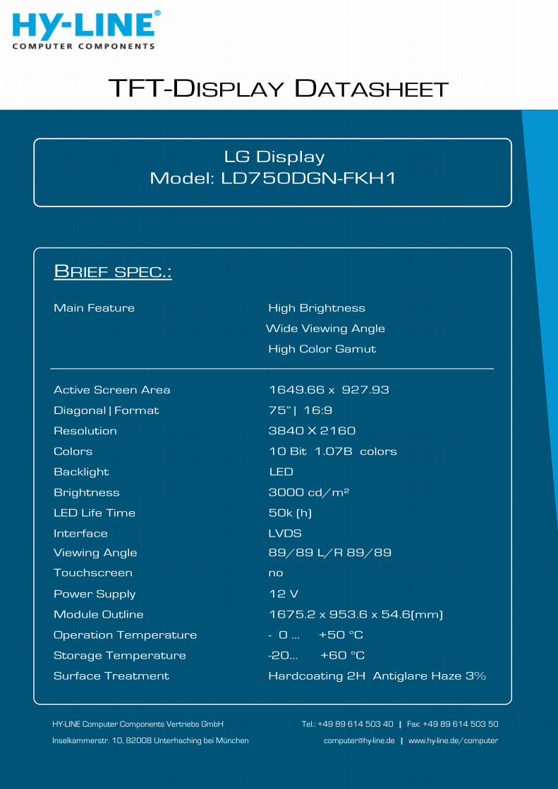
Title 75.0” QWUXGA TFT LCD
BUYER Hy-Line
MODEL
SUPPLIER LG Display Co., Ltd.
*MODEL LD750DGN
SUFFIX FKH1 (RoHS Verified)
SPECIFICATION
FOR
APPROVAL
APPROVED BY
SIGNATURE
DATE
Sungjun Lee / Team Leader
REVIEWED BY
Dongsan Kim / Project Leader
PREPARED BY
Youngjoo Hong / Engineer
TV Product Development Dept. LG Display Co., Ltd.
APPROVED BY SIGNATURE
DATE
/
/
/
Please return 1 copy for your confirmation with
your signature and comments.
( ) Preliminary Specification
( ) Final Specification
0 /40
Product Specification
LD750DGN
Ver. 1.1
CONTENTS
Number ITEM Page
COVER -
CONTENTS 1
RECORD OF REVISIONS 2
1 GENERAL DESCRIPTION 3
2 ABSOLUTE MAXIMUM RATINGS 4
3 ELECTRICAL SPECIFICATIONS 5
3-1 ELECTRICAL CHARACTERISTICS 5
3-2 INTERFACE CONNECTIONS 7
3-3 SIGNAL TIMING SPECIFICATIONS 11
3-4 V by One SIGNAL SPECIFICATIONS 12
3-5 COLOR DATA REFERENCE 14
3-6 POWER SEQUENCE 15
4 OPTICAL SPECIFICATIONS 17
5 MECHANICAL CHARACTERISTICS 21
6 RELIABILITY 24
7 INTERNATIONAL STANDARDS 25
7-1 SAFETY 25
7-2 ENVIRONMENT 25
8 PACKING 26
8-1 INFORMATION OF LCM LABEL 26
8-2 PACKING FORM 26
9 PRECAUTIONS 27
9-1 MOUNTING PRECAUTIONS 27
9-2 OPERATING PRECAUTIONS 27
9-3 ELECTROSTATIC DISCHARGE CONTROL 28
9-4 PRECAUTIONS FOR STRONG LIGHT EXPOSURE 28
9-5 STORAGE 28
9-6 APPROPRIATE CONDITION FOR COMMERCIAL DISPLAY 28
1 /40
Product Specification
LD750DGN
Ver. 1.1
Revision No. Revision Date Page Description
1.1 Jul. 21. 2016
RECORD OF REVISIONS
2 /40
Product Specification
LD750DGN
Ver. 1.1
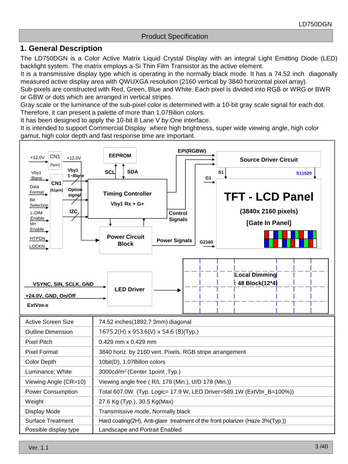
Active Screen Size 74.52 inches(1892.7 3mm) diagonal
Outline Dimension 1675.2(H) x 953.6(V) x 54.6 (B)(Typ.)
Pixel Pitch 0.429 mm x 0.429 mm
Pixel Format 3840 horiz. by 2160 vert. Pixels, RGB stripe arrangement
Color Depth 10bit(D), 1.07Billon colors
Luminance, White 3000cd/m2 (Center 1point ,Typ.)
Viewing Angle (CR>10) Viewing angle free ( R/L 178 (Min.), U/D 178 (Min.))
Power Consumption Total 607.0W (Typ. Logic= 17.9 W, LED Driver=589.1W (ExtVbr_B=100%))
Weight 27.6 Kg (Typ.), 30.5 Kg(Max)
Display Mode Transmissive mode, Normally black
Surface Treatment Hard coating(2H), Anti-glare treatment of the front polarizer (Haze 3%(Typ.))
Possible display type Landscape and Portrait Enabled
1. General Description
The LD750DGN is a Color Active Matrix Liquid Crystal Display with an integral Light Emitting Diode (LED)
backlight system. The matrix employs a-Si Thin Film Transistor as the active element.
It is a transmissive display type which is operating in the normally black mode. It has a 74.52 inch diagonally
measured active display area with QWUXGA resolution (2160 vertical by 3840 horizontal pixel array).
Sub-pixels are constructed with Red, Green, Blue and White. Each pixel is divided into RGB or WRG or BWR
or GBW or dots which are arranged in vertical stripes.
Gray scale or the luminance of the sub-pixel color is determined with a 10-bit gray scale signal for each dot.
Therefore, it can present a palette of more than 1.07Bilion colors.
It has been designed to apply the 10-bit 8 Lane V by One interface.
It is intended to support Commercial Display where high brightness, super wide viewing angle, high color
gamut, high color depth and fast response time are important.
Local Dimming
: 48 Block(12*4) LED Driver
+24.0V, GND, On/Off
ExtVBR-B
VSYNC, SIN, SCLK, GND
3 /40
Source Driver Circuit
TFT - LCD Panel (3840x 2160 pixels)
[Gate In Panel]
S1 S11520
EPI(RGBW)
Timing Controller
Vby1 Rx + G+
EEPROM
Power Circuit
Block
SDA SCL
CN1
(51pin)
Control
Signals
Power Signals
Vby1
1~8lane
Option
signal
I2C
G1
G2160
+12.0V CN1
(5pin)
+12.0V
Data
Format
Vby1
8lane
Bit
Selection
HTPDN
LOCKN
L-DIM
Enable
M+
Enable
Product Specification
LD750DGN
Ver. 1.1
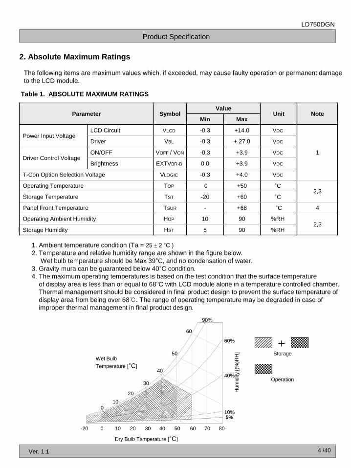
The following items are maximum values which, if exceeded, may cause faulty operation or permanent damage
to the LCD module.
2. Absolute Maximum Ratings
Table 1. ABSOLUTE MAXIMUM RATINGS
1. Ambient temperature condition (Ta = 25 2 °C )
2. Temperature and relative humidity range are shown in the figure below.
Wet bulb temperature should be Max 39°C, and no condensation of water.
3. Gravity mura can be guaranteed below 40°C condition.
4. The maximum operating temperatures is based on the test condition that the surface temperature
of display area is less than or equal to 68°C with LCD module alone in a temperature controlled chamber.
Thermal management should be considered in final product design to prevent the surface temperature of
display area from being over 68. The range of operating temperature may be degraded in case of
improper thermal management in final product design.
Note
Parameter Symbol Value
Unit Note Min Max
Power Input Voltage LCD Circuit VLCD -0.3 +14.0 VDC
1
Driver VBL -0.3 + 27.0 VDC
Driver Control Voltage ON/OFF VOFF / VON -0.3 +3.9 VDC
Brightness EXTVBR-B 0.0 +3.9 VDC
T-Con Option Selection Voltage VLOGIC -0.3 +4.0 VDC
Operating Temperature TOP 0 +50 °C 2,3
Storage Temperature TST -20 +60 °C
Panel Front Temperature TSUR - +68 °C 4
Operating Ambient Humidity HOP 10 90 %RH 2,3
Storage Humidity HST 5 90 %RH
90%
10 20 30 40 50 60 70 80 0 -20
0 10
20
30
40
50
Dry Bulb Temperature [°C]
Wet Bulb
Temperature [°C]
Storage
Operation
Hum
idity [(%
)RH
]
10%
40%
60%
60
5%
4 /40
Product Specification
LD750DGN
Ver. 1.1
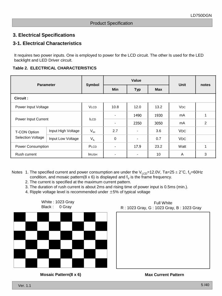
3. Electrical Specifications
3-1. Electrical Characteristics
It requires two power inputs. One is employed to power for the LCD circuit. The other Is used for the LED
backlight and LED Driver circuit.
Table 2. ELECTRICAL CHARACTERISTICS
5 /40
Parameter Symbol
Value
Unit notes
Min Typ Max
Circuit :
Power Input Voltage VLCD 10.8 12.0 13.2 VDC
Power Input Current ILCD
- 1490 1930 mA 1
- 2350 3050 mA 2
T-CON Option
Selection Voltage
Input High Voltage VIH 2.7 - 3.6 VDC
Input Low Voltage VIL 0 - 0.7 VDC
Power Consumption PLCD - 17.9 23.2 Watt 1
Rush current IRUSH - - 10 A 3
Notes 1. The specified current and power consumption are under the VLCD=12.0V, Ta=25 2°C, fV=60Hz
condition, and mosaic pattern(8 x 6) is displayed and fV is the frame frequency.
2. The current is specified at the maximum current pattern.
3. The duration of rush current is about 2ms and rising time of power input is 0.5ms (min.).
4. Ripple voltage level is recommended under ±5% of typical voltage
White : 1023 Gray
Black : 0 Gray
Mosaic Pattern(8 x 6) Max Current Pattern
Full White
R : 1023 Gray, G : 1023 Gray, B : 1023 Gray
Product Specification
LD750DGN
Ver. 1.1
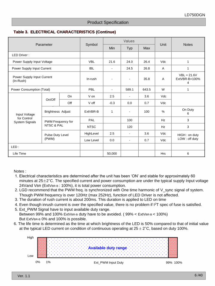
Table 3. ELECTRICAL CHARACTERISTICS (Continue) Table 3. ELECTRICAL CHARACTERISTICS (Continue)
Parameter Symbol Values
Unit Notes Min Typ Max
LED Driver :
Power Supply Input Voltage VBL 21.6 24.0 26.4 Vdc 1
Power Supply Input Current IBL - 24.5 26.8 A 1
Power Supply Input Current
(In-Rush) In-rush - - 35.8 A
VBL = 21.6V
ExtVBR-B=100%
4
Power Consumption (Total) PBL - 589.1 643.5 W 1
Input Voltage
for Control
System Signals
On/Off On V on 2.5 - 3.6 Vdc
Off V off -0.3 0.0 0.7 Vdc
Brightness Adjust ExtVBR-B 1 - 100 % On Duty
6
PWM Frequency for
NTSC & PAL
PAL 100 Hz 3
NTSC 120 Hz 3
Pulse Duty Level
(PWM)
HighLevel 2.5 - 3.6 Vdc HIGH : on duty
LOW : off duty Low Level 0.0 - 0.7 Vdc
LED :
Life Time 50,000 Hrs 6
6 /40
Available duty range
High
Low
0% 1% 99% 100% Ext_PWM Input Duty
Notes :
1. Electrical characteristics are determined after the unit has been ‘ON’ and stable for approximately 60
minutes at 25±2°C. The specified current and power consumption are under the typical supply Input voltage
24Vand VBR (ExtVBR-B : 100%), it is total power consumption. 2. LGD recommend that the PWM freq. is synchronized with One time harmonic of V_sync signal of system.
Though PWM frequency is over 120Hz (max 252Hz), function of LED Driver is not affected. 3. The duration of rush current is about 200ms. This duration is applied to LED on time
4. Even though inrush current is over the specified value, there is no problem if I2T spec of fuse is satisfied.
5. Ext_PWM Signal have to input available duty range.
Between 99% and 100% ExtVBR-B duty have to be avoided. ( 99% < ExtVBR-B < 100%)
But ExtVBR-B 0% and 100% is possible.
6. The life time is determined as the time at which brightness of the LED is 50% compared to that of initial value
at the typical LED current on condition of continuous operating at 25 2°C, based on duty 100%.
Product Specification
LD750DGN
Ver. 1.1
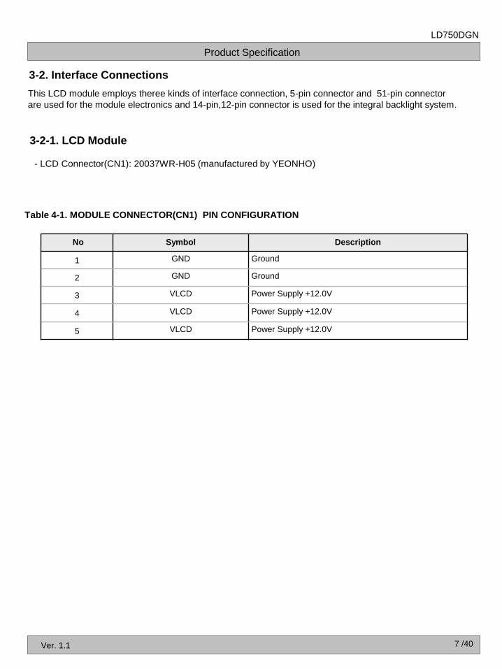
3-2. Interface Connections
This LCD module employs theree kinds of interface connection, 5-pin connector and 51-pin connector
are used for the module electronics and 14-pin,12-pin connector is used for the integral backlight system.
3-2-1. LCD Module
- LCD Connector(CN1): 20037WR-H05 (manufactured by YEONHO)
No Symbol Description
1 GND Ground
2 GND Ground
3 VLCD Power Supply +12.0V
4 VLCD Power Supply +12.0V
5 VLCD Power Supply +12.0V
Table 4-1. MODULE CONNECTOR(CN1) PIN CONFIGURATION
7 /40
Product Specification
LD750DGN
Ver. 1.1
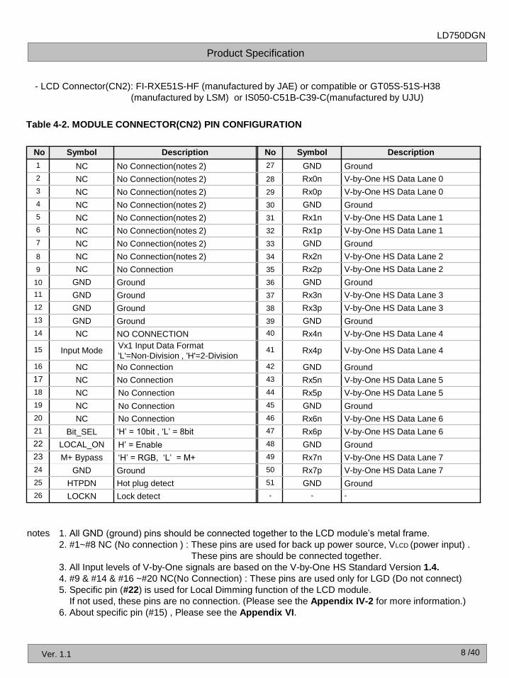
Table 4-2. MODULE CONNECTOR(CN2) PIN CONFIGURATION
- LCD Connector(CN2): FI-RXE51S-HF (manufactured by JAE) or compatible or GT05S-51S-H38
(manufactured by LSM) or IS050-C51B-C39-C(manufactured by UJU)
notes
No Symbol Description No Symbol Description
1 NC No Connection(notes 2) 27 GND Ground
2 NC No Connection(notes 2) 28 Rx0n V-by-One HS Data Lane 0
3 NC No Connection(notes 2) 29 Rx0p V-by-One HS Data Lane 0
4 NC No Connection(notes 2) 30 GND Ground
5 NC No Connection(notes 2) 31 Rx1n V-by-One HS Data Lane 1
6 NC No Connection(notes 2) 32 Rx1p V-by-One HS Data Lane 1
7 NC No Connection(notes 2) 33 GND Ground
8 NC No Connection(notes 2) 34 Rx2n V-by-One HS Data Lane 2
9 NC No Connection 35 Rx2p V-by-One HS Data Lane 2
10 GND Ground 36 GND Ground
11 GND Ground 37 Rx3n V-by-One HS Data Lane 3
12 GND Ground 38 Rx3p V-by-One HS Data Lane 3
13 GND Ground 39 GND Ground
14 NC NO CONNECTION 40 Rx4n V-by-One HS Data Lane 4
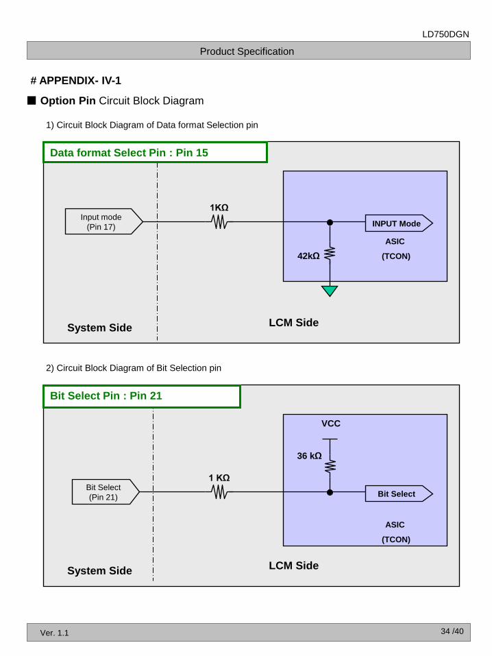
15 Input Mode Vx1 Input Data Format
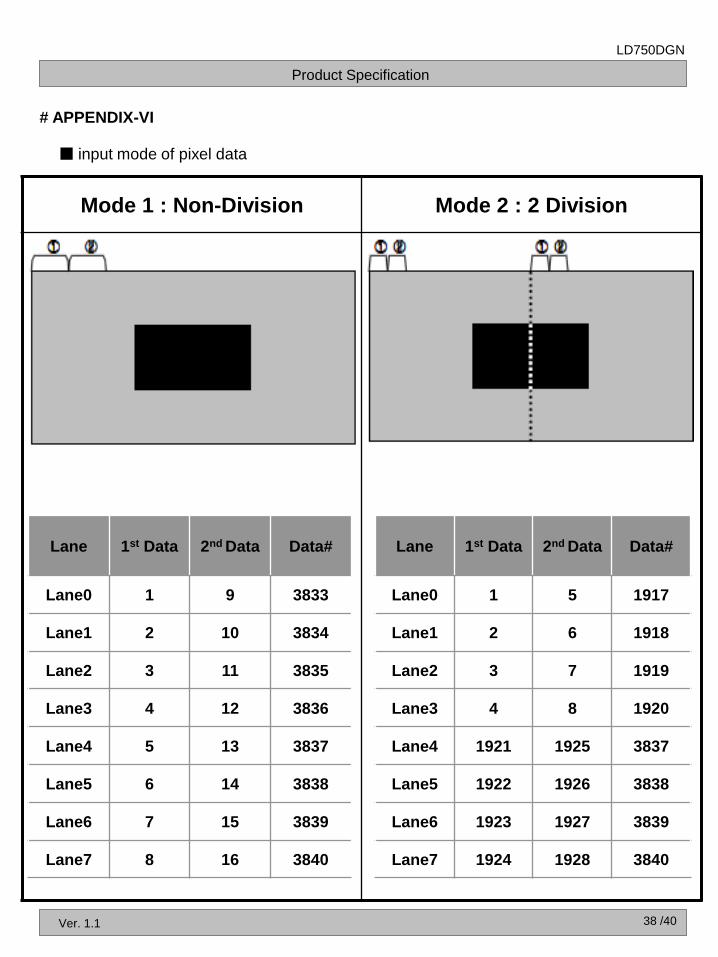
'L'=Non-Division , 'H'=2-Division 41 Rx4p V-by-One HS Data Lane 4
16 NC No Connection 42 GND Ground
17 NC No Connection 43 Rx5n V-by-One HS Data Lane 5
18 NC No Connection 44 Rx5p V-by-One HS Data Lane 5
19 NC No Connection 45 GND Ground
20 NC No Connection 46 Rx6n V-by-One HS Data Lane 6
21 Bit_SEL ‘H’ = 10bit , ‘L’ = 8bit 47 Rx6p V-by-One HS Data Lane 6
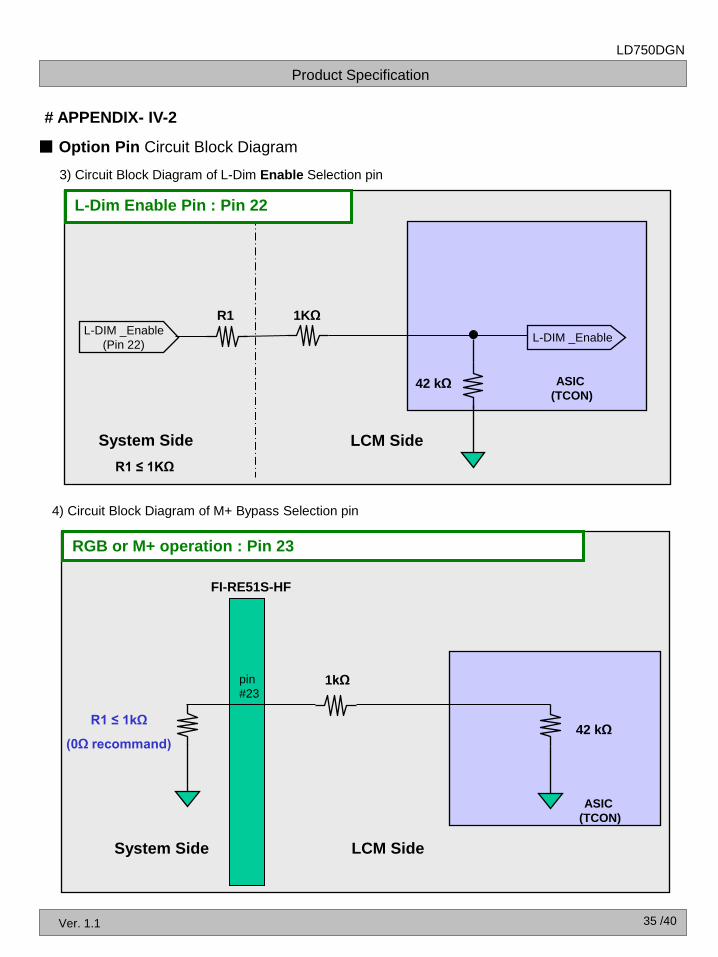
22 LOCAL_ON H’ = Enable 48 GND Ground
23 M+ Bypass ‘H’ = RGB, ‘L’ = M+ 49 Rx7n V-by-One HS Data Lane 7
24 GND Ground 50 Rx7p V-by-One HS Data Lane 7
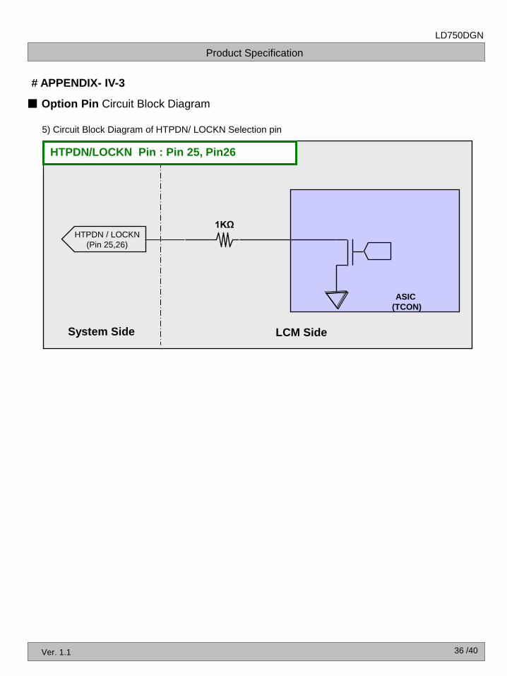
25 HTPDN Hot plug detect 51 GND Ground
26 LOCKN Lock detect - - -
8 /40
1. All GND (ground) pins should be connected together to the LCD module’s metal frame.
2. #1~#8 NC (No connection ) : These pins are used for back up power source, VLCD (power input) .
These pins are should be connected together.
3. All Input levels of V-by-One signals are based on the V-by-One HS Standard Version 1.4.
4. #9 & #14 & #16 ~#20 NC(No Connection) : These pins are used only for LGD (Do not connect)
5. Specific pin (#22) is used for Local Dimming function of the LCD module.
If not used, these pins are no connection. (Please see the Appendix IV-2 for more information.)
6. About specific pin (#15) , Please see the Appendix VI.
Product Specification
LD750DGN
Ver. 1.1
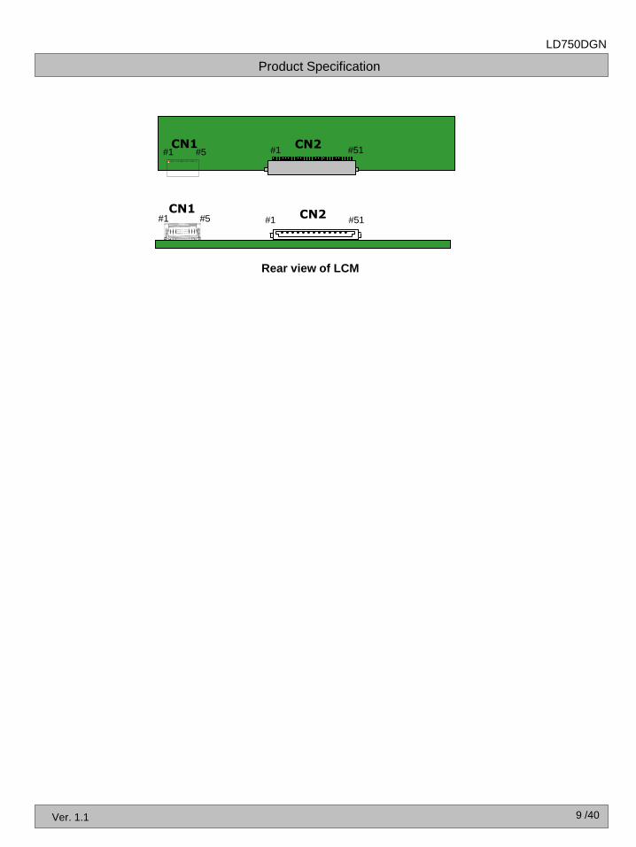
CN2 #1 #51
Rear view of LCM
#1 #51 CN2 #1 #5
CN1
#1 CN1
#5
9 /40
Product Specification
LD750DGN
Ver. 1.1
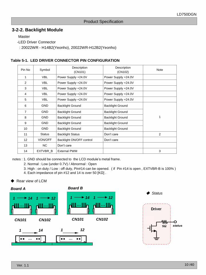
3-2-2. Backlight Module
10 /40
Table 5-1. LED DRIVER CONNECTOR PIN CONFIGURATION
Rear view of LCM
Master
-LED Driver Connector
: 20022WR - H14B2(Yeonho), 20022WR-H12B2(Yeonho)
notes : 1. GND should be connected to the LCD module’s metal frame.
2. Normal : Low (under 0.7V) / Abnormal : Open
3. High : on duty / Low : off duty, Pin#14 can be opened. ( if Pin #14 is open , EXTVBR-B is 100% )
4. Each impedance of pin #12 and 14 is over 50 [KΩ] .
Pin No Symbol Description
(CN101)
Description
(CN102) Note
1 VBL Power Supply +24.0V Power Supply +24.0V
2 VBL Power Supply +24.0V Power Supply +24.0V
3 VBL Power Supply +24.0V Power Supply +24.0V
4 VBL Power Supply +24.0V Power Supply +24.0V
5 VBL Power Supply +24.0V Power Supply +24.0V
6 GND Backlight Ground Backlight Ground
1
7 GND Backlight Ground Backlight Ground
8 GND Backlight Ground Backlight Ground
9 GND Backlight Ground Backlight Ground
10 GND Backlight Ground Backlight Ground
11 Status Backlight Status Don’t care 2
12 VON/OFF Backlight ON/OFF control Don’t care
13 NC Don’t care
14 EXTVBR_B External PWM 3
Board A
1 14 1 12
CN101 CN102
Board B
1 14 1 12
CN101 CN102
… …
14 1 12 1
Status
Product Specification
LD750DGN
Ver. 1.1
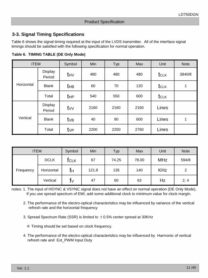
3-3. Signal Timing Specifications
Table 6 shows the signal timing required at the input of the LVDS transmitter. All of the interface signal
timings should be satisfied with the following specification for normal operation.
Table 6. TIMING TABLE (DE Only Mode)
notes: 1. The input of HSYNC & VSYNC signal does not have an effect on normal operation (DE Only Mode).
If you use spread spectrum of EMI, add some additional clock to minimum value for clock margin.
2. The performance of the electro-optical characteristics may be influenced by variance of the vertical
refresh rate and the horizontal frequency
3. Spread Spectrum Rate (SSR) is limited to ±0.5% center spread at 30KHz
※ Timing should be set based on clock frequency.
4. The performance of the electro-optical characteristics may be influenced by Harmonic of vertical
refresh rate and Ext_PWM Input Duty
ITEM Symbol Min Typ Max Unit Note
Horizontal
Display
Period tHV 480 480 480 tCLK 3840/8
Blank tHB 60 70 120 tCLK 1
Total tHP 540 550 600 tCLK
Vertical
Display
Period tVV 2160 2160 2160 Lines
Blank tVB 40 90 600 Lines 1
Total tVP 2200 2250 2760 Lines
ITEM Symbol Min Typ Max Unit Note
Frequency
DCLK fCLK 67 74.25 78.00 MHz 594/8
Horizontal fH 121.8 135 140 KHz 2
Vertical fV 47 60 63 Hz 2, 4
11 /40
Product Specification
LD750DGN
Ver. 1.1
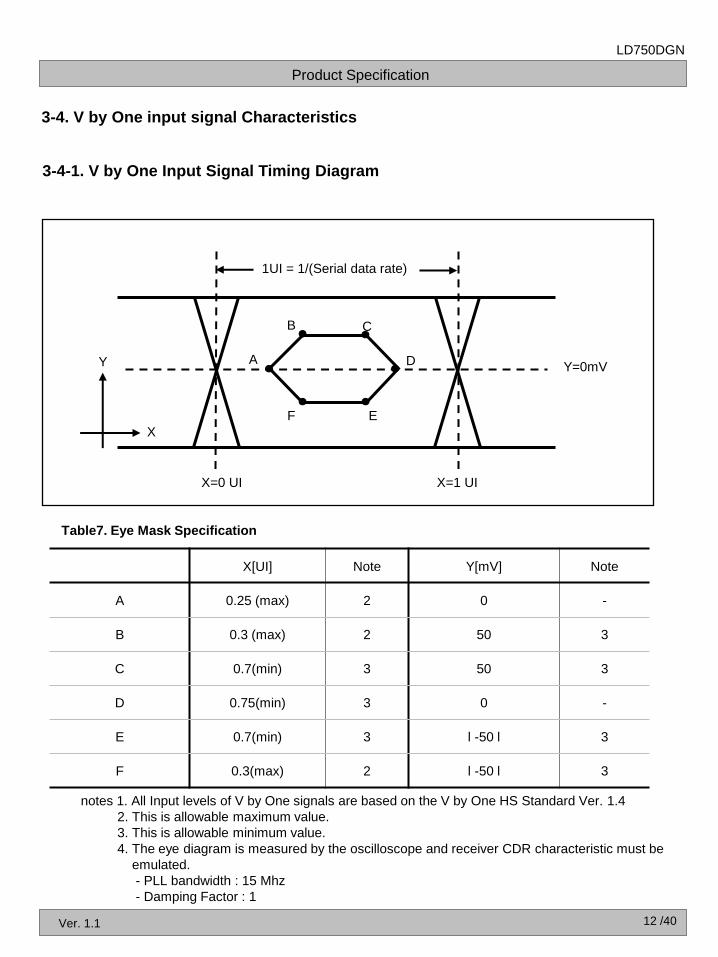
3-4-1. V by One Input Signal Timing Diagram
A
B
F E
D
C
ㆍ ㆍ
ㆍ ㆍ ㆍ
ㆍ Y=0mV
X=0 UI X=1 UI
1UI = 1/(Serial data rate)
Y
X
X[UI] Note Y[mV] Note
A 0.25 (max) 2 0 -
B 0.3 (max) 2 50 3
C 0.7(min) 3 50 3
D 0.75(min) 3 0 -
E 0.7(min) 3 l -50 l 3
F 0.3(max) 2 l -50 l 3
Table7. Eye Mask Specification
3-4. V by One input signal Characteristics
notes 1. All Input levels of V by One signals are based on the V by One HS Standard Ver. 1.4
2. This is allowable maximum value.
3. This is allowable minimum value.
4. The eye diagram is measured by the oscilloscope and receiver CDR characteristic must be
emulated.
- PLL bandwidth : 15 Mhz
- Damping Factor : 1
12 /40
Product Specification
LD750DGN
Ver. 1.1
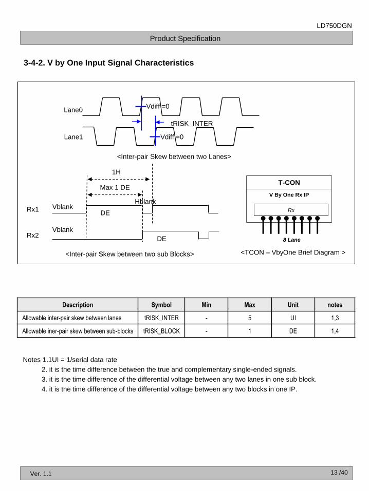
3-4-2. V by One Input Signal Characteristics
tRISK_INTER
Lane0
Lane1
Vdiff =0
Vdiff =0
Description Symbol Min Max Unit notes
Allowable inter-pair skew between lanes tRISK_INTER - 5 UI 1,3
Allowable iner-pair skew between sub-blocks tRISK_BLOCK - 1 DE 1,4
<Inter-pair Skew between two Lanes>
<Inter-pair Skew between two sub Blocks>
Notes 1.1UI = 1/serial data rate
2. it is the time difference between the true and complementary single-ended signals.
3. it is the time difference of the differential voltage between any two lanes in one sub block.
4. it is the time difference of the differential voltage between any two blocks in one IP.
Rx1 Vblank Hblank
Rx2 Vblank
DE
Max 1 DE
DE
1H
<TCON – VbyOne Brief Diagram >
T-CON
V By One Rx IP
Rx
8 Lane
13 /40
Product Specification
LD750DGN
Ver. 1.1
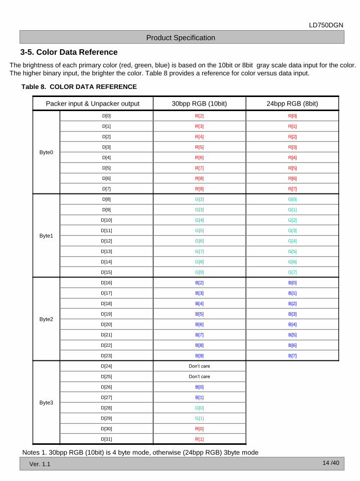
3-5. Color Data Reference
The brightness of each primary color (red, green, blue) is based on the 10bit or 8bit gray scale data input for the color.
The higher binary input, the brighter the color. Table 8 provides a reference for color versus data input.
Table 8. COLOR DATA REFERENCE
Packer input & Unpacker output 30bpp RGB (10bit) 24bpp RGB (8bit)
Byte0
D[0] R[2] R[0]
D[1] R[3] R[1]
D[2] R[4] R[2]
D[3] R[5] R[3]
D[4] R[6] R[4]
D[5] R[7] R[5]
D[6] R[8] R[6]
D[7] R[9] R[7]
Byte1
D[8] G[2] G[0]
D[9] G[3] G[1]
D[10] G[4] G[2]
D[11] G[5] G[3]
D[12] G[6] G[4]
D[13] G[7] G[5]
D[14] G[8] G[6]
D[15] G[9] G[7]
Byte2
D[16] B[2] B[0]
D[17] B[3] B[1]
D[18] B[4] B[2]
D[19] B[5] B[3]
D[20] B[6] B[4]
D[21] B[7] B[5]
D[22] B[8] B[6]
D[23] B[9] B[7]
Byte3
D[24] Don’t care
D[25] Don’t care
D[26] B[0]
D[27] B[1]
D[28] G[0]
D[29] G[1]
D[30] R[0]
D[31] R[1]
Notes 1. 30bpp RGB (10bit) is 4 byte mode, otherwise (24bpp RGB) 3byte mode
14 /40
Product Specification
LD750DGN
Ver. 1.1
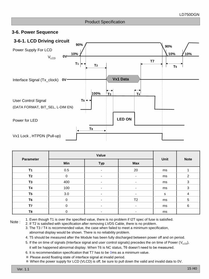
Note : 1. Even though T1 is over the specified value, there is no problem if I2T spec of fuse is satisfied.
2. If T2 is satisfied with specification after removing LVDS Cable, there is no problem.
3. The T3 / T4 is recommended value, the case when failed to meet a minimum specification,
abnormal display would be shown. There is no reliability problem.
4. T5 should be measured after the Module has been fully discharged between power off and on period.
5. If the on time of signals (Interface signal and user control signals) precedes the on time of Power (VLCD),
it will be happened abnormal display. When T6 is NC status, T6 doesn’t need to be measured.
6. It is recommendation specification that T7 has to be 0ms as a minimum value.
※ Please avoid floating state of interface signal at invalid period.
※ When the power supply for LCD (VLCD) is off, be sure to pull down the valid and invalid data to 0V.
15 /40
10% 0V
90%
10%
T1 T2 T5
LED ON
T3 T4
T6
Interface Signal (Tx_clock)
Power for LED
Power Supply For LCD
VLCD
User Control Signal
(DATA FORMAT, BIT_SEL, L-DIM EN)
0V Vx1 Data
100%
10%
90%
T7
T8
Vx1 Lock , HTPDN (Pull-up)
Parameter Value
Unit Note Min Typ Max
T1 0.5 - 20 ms 1
T2 0 - - ms 2
T3 400 - - ms 3
T4 100 - - ms 3
T5 3.0 - - s 4
T6 0 - T2 ms 5
T7 0 - - ms 6
T8 0 - - ms
3-6-1. LCD Driving circuit
3-6. Power Sequence
Product Specification
LD750DGN
Ver. 1.1 16 /40
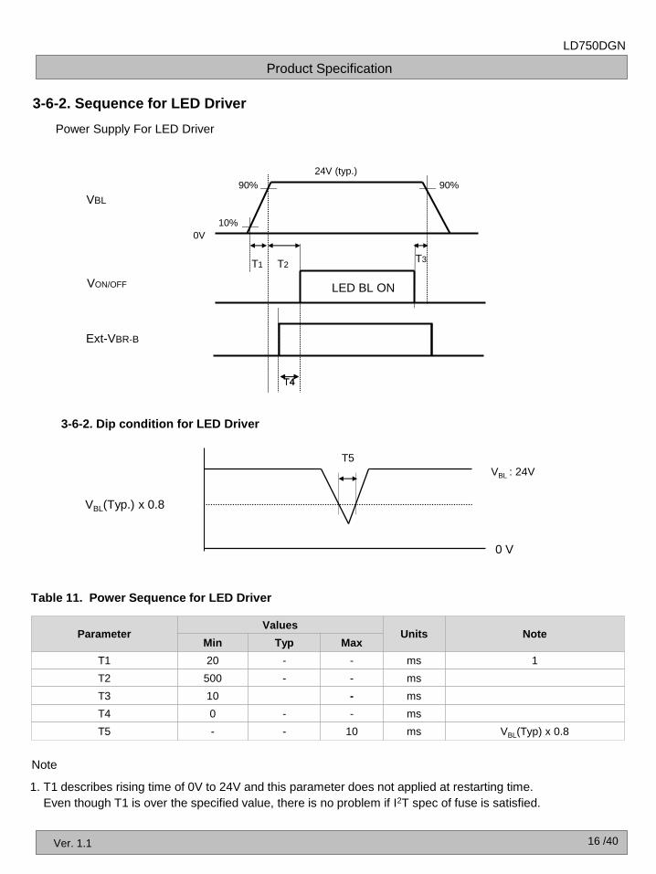
1. T1 describes rising time of 0V to 24V and this parameter does not applied at restarting time.
Even though T1 is over the specified value, there is no problem if I2T spec of fuse is satisfied.
Power Supply For LED Driver
VON/OFF
VBL
10%
0V
90%
T1 T2
24V (typ.)
T3
LED BL ON
Table 11. Power Sequence for LED Driver
90%
T4
Ext-VBR-B
3-6-2. Dip condition for LED Driver
VBL(Typ.) x 0.8
0 V
VBL : 24V
T5
Parameter Values
Units Note Min Typ Max
T1 20 - - ms 1
T2 500 - - ms
T3 10 - ms
T4 0 - - ms
T5 - - 10 ms VBL(Typ) x 0.8
T4
Note
3-6-2. Sequence for LED Driver
Product Specification
LD750DGN
Ver. 1.1
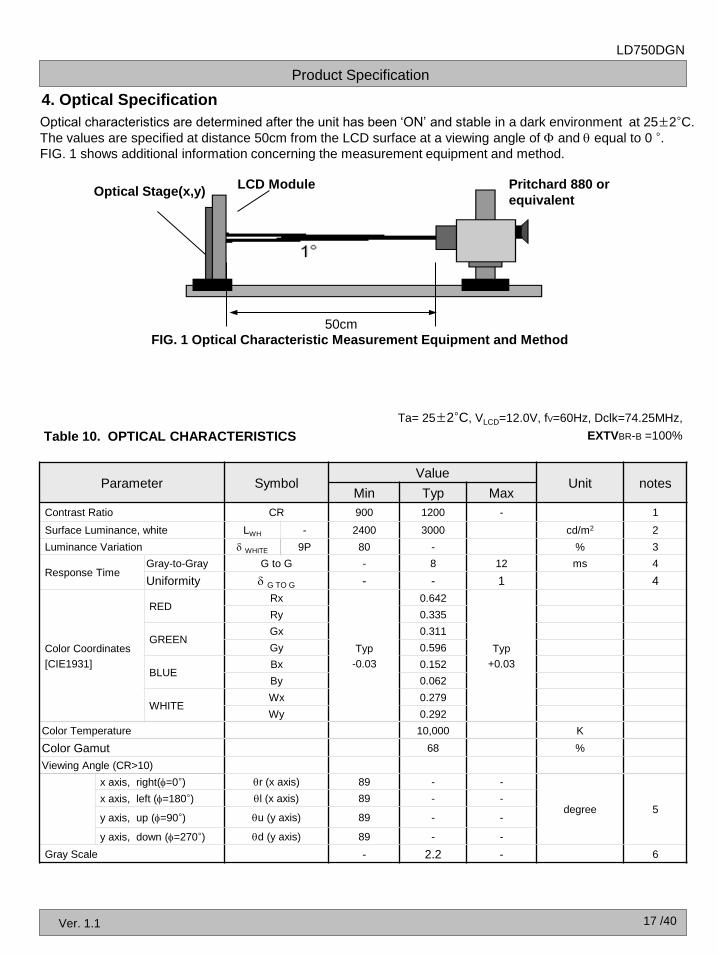
LCD Module Optical Stage(x,y)
Pritchard 880 or
equivalent
50cm FIG. 1 Optical Characteristic Measurement Equipment and Method
4. Optical Specification
Optical characteristics are determined after the unit has been ‘ON’ and stable in a dark environment at 25±2°C.
The values are specified at distance 50cm from the LCD surface at a viewing angle of and equal to 0 °. FIG. 1 shows additional information concerning the measurement equipment and method.
Parameter Symbol Value
Unit notes Min Typ Max
Contrast Ratio CR 900 1200 - 1
Surface Luminance, white LWH - 2400 3000 cd/m2 2
Luminance Variation WHITE 9P 80 - % 3
Response Time Gray-to-Gray G to G - 8 12 ms 4
Uniformity G TO G - - 1 4
Color Coordinates
[CIE1931]
RED Rx
Typ
-0.03
0.642
Typ
+0.03
Ry 0.335
GREEN Gx 0.311
Gy 0.596
BLUE Bx 0.152
By 0.062
WHITE Wx 0.279
Wy 0.292
Color Temperature 10,000 K
Color Gamut 68 %
Viewing Angle (CR>10)
x axis, right(=0°) r (x axis) 89 - -
degree 5 x axis, left (=180°) l (x axis) 89 - -
y axis, up (=90°) u (y axis) 89 - -
y axis, down (=270°) d (y axis) 89 - -
Gray Scale - 2.2 - 6
Table 10. OPTICAL CHARACTERISTICS
Ta= 25±2°C, VLCD=12.0V, fV=60Hz, Dclk=74.25MHz,
EXTVBR-B =100%
17 /40
Product Specification
LD750DGN
Ver. 1.1
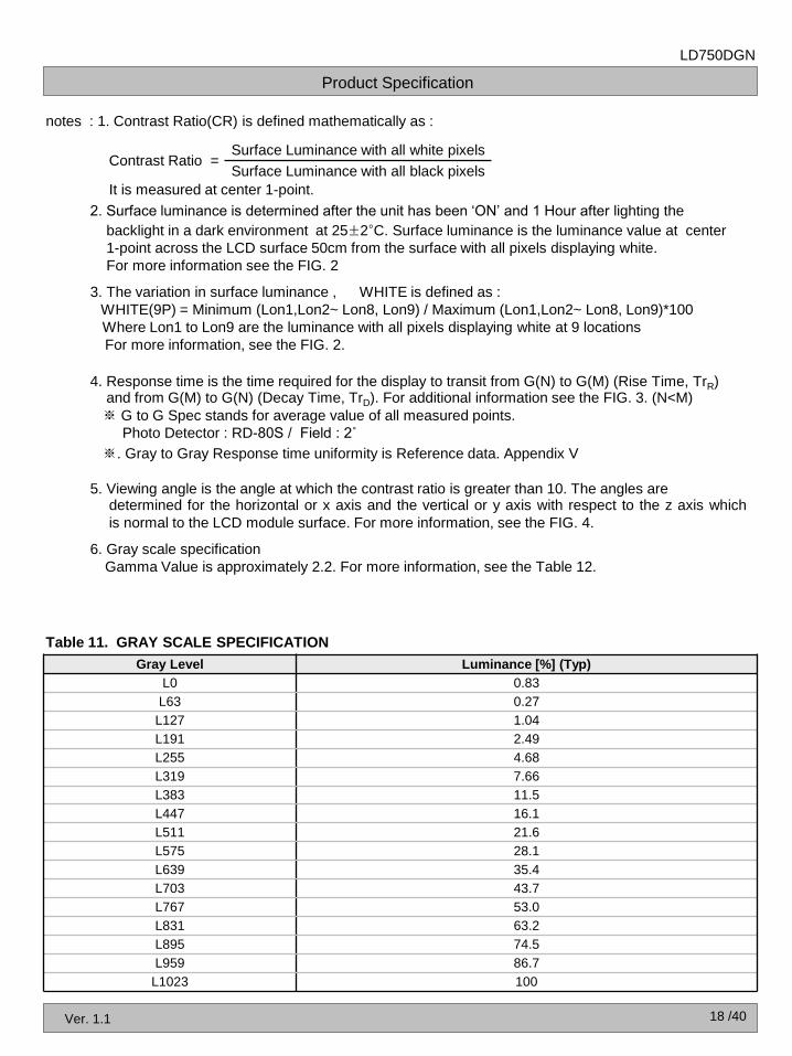
Table 11. GRAY SCALE SPECIFICATION
Gray Level Luminance [%] (Typ)
L0 0.83
L63 0.27
L127 1.04
L191 2.49
L255 4.68
L319 7.66
L383 11.5
L447 16.1
L511 21.6
L575 28.1
L639 35.4
L703 43.7
L767 53.0
L831 63.2
L895 74.5
L959 86.7
L1023 100
18 /40
notes : 1. Contrast Ratio(CR) is defined mathematically as :
Surface Luminance with all white pixels Contrast Ratio = Surface Luminance with all black pixels
It is measured at center 1-point.
2. Surface luminance is determined after the unit has been ‘ON’ and 1 Hour after lighting the
backlight in a dark environment at 25±2°C. Surface luminance is the luminance value at center
1-point across the LCD surface 50cm from the surface with all pixels displaying white.
For more information see the FIG. 2 3. The variation in surface luminance , WHITE is defined as :
WHITE(9P) = Minimum (Lon1,Lon2~ Lon8, Lon9) / Maximum (Lon1,Lon2~ Lon8, Lon9)*100
Where Lon1 to Lon9 are the luminance with all pixels displaying white at 9 locations
For more information, see the FIG. 2.
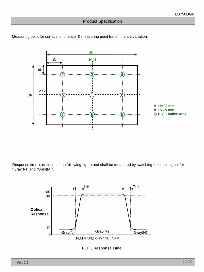
4. Response time is the time required for the display to transit from G(N) to G(M) (Rise Time, TrR) and from G(M) to G(N) (Decay Time, TrD). For additional information see the FIG. 3. (N<M)
※ G to G Spec stands for average value of all measured points.
Photo Detector : RD-80S / Field : 2˚
※. Gray to Gray Response time uniformity is Reference data. Appendix V
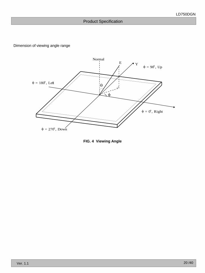
5. Viewing angle is the angle at which the contrast ratio is greater than 10. The angles are determined for the horizontal or x axis and the vertical or y axis with respect to the z axis which
is normal to the LCD module surface. For more information, see the FIG. 4. 6. Gray scale specification
Gamma Value is approximately 2.2. For more information, see the Table 12.
Product Specification
LD750DGN
Ver. 1.1 19 /40
FIG. 3 Response Time
Response time is defined as the following figure and shall be measured by switching the input signal for
“Gray(N)” and “Gray(M)”.
Measuring point for surface luminance & measuring point for luminance variation.
Gray(M) Gray(N)
TrR TrD
100 90
10
0
Optical
Response
N,M = Black~White, N<M
Gray(N)
A : H / 9 mm
B : V / 9 mm
@ H,V : Active Area
H
A
V
B
①
② ③ ④
⑦ ⑧ ⑨
⑤ ⑥
H / 2
V / 2
Product Specification
LD750DGN
Ver. 1.1
FIG. 4 Viewing Angle
Dimension of viewing angle range
Normal
Y E
= 0, Right
= 180, Left
= 270, Down
= 90, Up
20 /40
Product Specification
LD750DGN
Ver. 1.1
Table 12 provides general mechanical characteristics.
5. Mechanical Characteristics
Table 12. MECHANICAL CHARACTERISTICS
notes : Please refer to a mechanical drawing in terms of tolerance at the next page.
21 /40
Item Value
Outline Dimension
Horizontal 1675.2mm
Vertical 953.6 mm
Depth 54.6 mm
Bezel Area Horizontal 1651.6 mm
Vertical 930. mm
Active Display Area Horizontal 1649.664mm
Vertical 927.936mm
Weight 27.6 Kg (Typ.), 30.5 Kg(Max)
Case Top
Material EGI
Case Top Color Black
LG Logo Color None
Ultra HD Logo Color None
Product Specification
LD750DGN
Ver. 1.1 22 /40
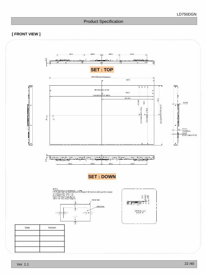
[ FRONT VIEW ]
Date Version
SET : TOP
SET : DOWN
Product Specification
LD750DGN
Ver. 1.1 23 /40 23 /40 23 /40
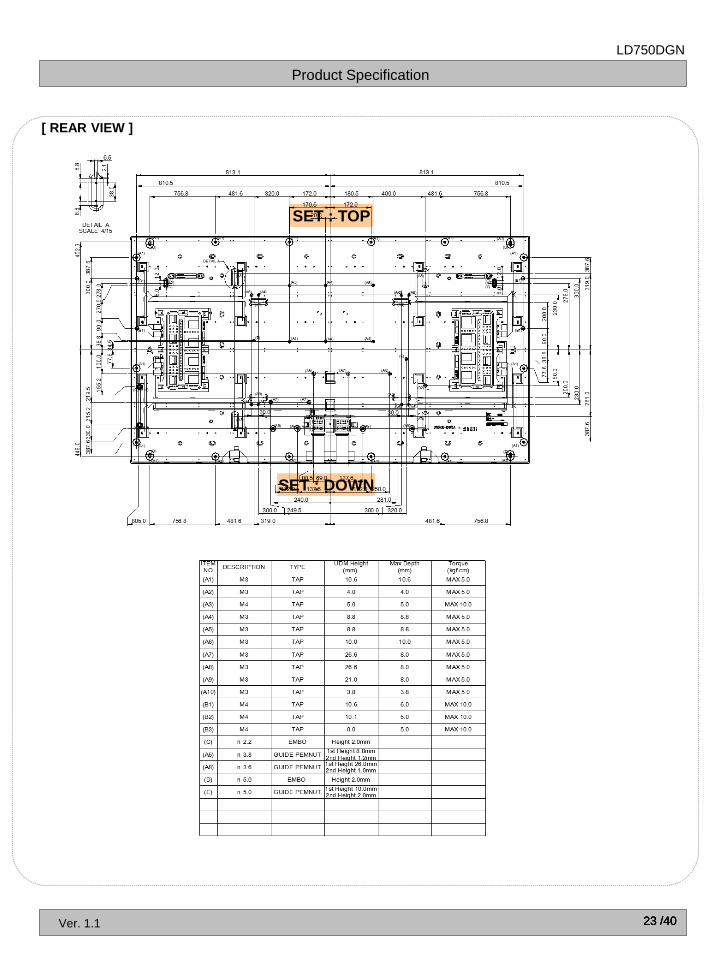
[ REAR VIEW ]
SET : TOP SET : TOP
SET : DOWN
Product Specification
LD750DGN
Ver. 1.1
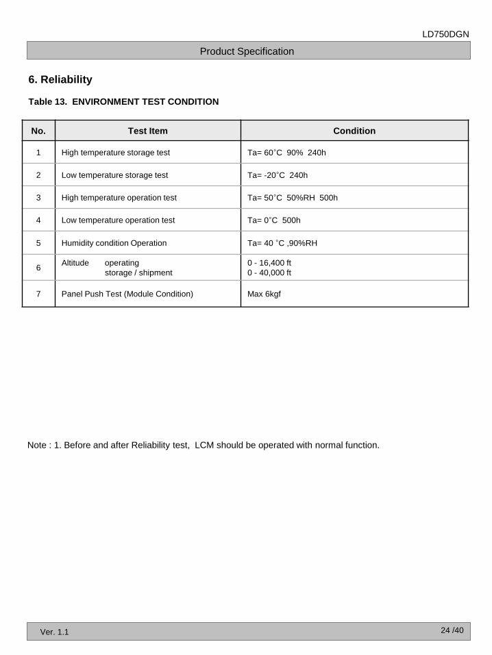
6. Reliability
Table 13. ENVIRONMENT TEST CONDITION
Note : 1. Before and after Reliability test, LCM should be operated with normal function.
24 /40
No. Test Item Condition
1 High temperature storage test Ta= 60°C 90% 240h
2 Low temperature storage test Ta= -20°C 240h
3 High temperature operation test Ta= 50°C 50%RH 500h
4 Low temperature operation test Ta= 0°C 500h
5 Humidity condition Operation Ta= 40 °C ,90%RH
6 Altitude operating
storage / shipment
0 - 16,400 ft
0 - 40,000 ft
7 Panel Push Test (Module Condition) Max 6kgf
Product Specification
LD750DGN
Ver. 1.1
7. International Standards
7-1. Safety
7-2. Environment
a) RoHS, Directive 2011/65/EU of the European Parliament and of the council of 8 June 2011
a) UL 60065, Underwriters Laboratories Inc.
Audio, Video and Similar Electronic Apparatus - Safety Requirements.
b) CAN/CSA C22.2 No.60065:03, Canadian Standards Association.
Audio, Video and Similar Electronic Apparatus - Safety Requirements.
c) EN 60065, European Committee for Electrotechnical Standardization (CENELEC).
Audio, Video and Similar Electronic Apparatus - Safety Requirements.
d) IEC 60065, The International Electrotechnical Commission (IEC).
Audio, Video and Similar Electronic Apparatus - Safety Requirements.
25 /40
Product Specification
LD750DGN
Ver. 1.1
8. Packing
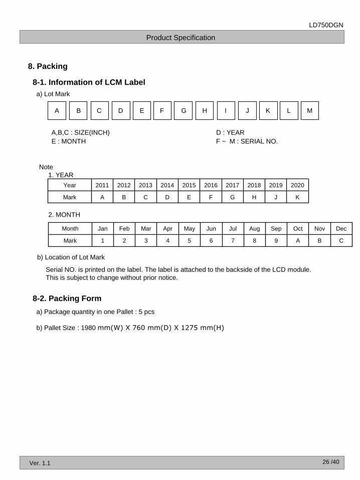
8-1. Information of LCM Label
26 /40
8-2. Packing Form
a) Package quantity in one Pallet : 5 pcs
b) Pallet Size : 1980 mm(W) X 760 mm(D) X 1275 mm(H)
a) Lot Mark
A B C D E F G H I J K L M
Note
1. YEAR
b) Location of Lot Mark
2. MONTH
Serial NO. is printed on the label. The label is attached to the backside of the LCD module.
This is subject to change without prior notice.
A,B,C : SIZE(INCH) D : YEAR
E : MONTH F ~ M : SERIAL NO.
Mark
Year
K
2020
F
2016
G
2017
H
2018
J
2019
D
2014
E
2015
C B A
2013 2012 2011
B
Nov
Mark
Month
A
Oct
6
Jun
7
Jul
8
Aug
9
Sep
4
Apr
5
May
C 3 2 1
Dec Mar Feb Jan
Product Specification
LD750DGN
Ver. 1.1
Please pay attention to the followings when you use this TFT LCD module.
9-1. Mounting Precautions
(1) You must mount a module using specified mounting holes (Details refer to the drawings).
(2) You should consider the mounting structure so that uneven force (ex. Twisted stress, Concentrated stress)
is not applied to the module. And the case on which a module is mounted should have sufficient strength
so that external force is not transmitted directly to the module.
(3) Please attach the surface transparent protective plate to the surface in order to protect the polarizer.
Transparent protective plate should have sufficient strength in order to the resist external force.
(4) You should adopt radiation structure to satisfy the temperature specification.
(5) Acetic acid type and chlorine type materials for the cover case are not desirable because the former
generates corrosive gas of attacking the polarizer at high temperature and the latter causes circuit break
by electro-chemical reaction.
(6) Do not touch, push or rub the exposed polarizers with glass, tweezers or anything harder than HB
pencil lead. And please do not rub with dust clothes with chemical treatment.
Do not touch the surface of polarizer for bare hand or greasy cloth.(Some cosmetics are detrimental
to the polarizer.)
(7) When the surface becomes dusty, please wipe gently with absorbent cotton or other soft materials like
chamois soaks with petroleum benzine. Normal-hexane is recommended for cleaning the adhesives
used to attach front / rear polarizers. Do not use acetone, toluene and alcohol because they cause
chemical damage to the polarizer
(8) Wipe off saliva or water drops as soon as possible. Their long time contact with polarizer causes
deformations and color fading.
(9) Do not open the case because inside circuits do not have sufficient strength.
(10) Touching the LED Driver might cause an electric shock and damage to LED Driver. Please always use
antistatic tools when handling the LED Driver
9. Precautions
9-2. Operating Precautions
(1) Response time depends on the temperature.(In lower temperature, it becomes longer.)
(2) Brightness depends on the temperature. (In lower temperature, it becomes lower.)
And in lower temperature, response time(required time that brightness is stable after turned on)
becomes longer
(3) Be careful for condensation at sudden temperature change.Condensation makes damage to polarizer or
electrical contacted parts. And after fading condensation, smear or spot will occur.
(4) When fixed patterns are displayed for a long time, remnant image is likely to occur.
(5) Module has high frequency circuits. Sufficient suppression to the electromagnetic interference shall be
done by system manufacturers. Grounding and shielding methods may be important to minimized the
interference.
(6) Please do not give any mechanical and/or acoustical impact to LCM. Otherwise, LCM can’t be operated
its full characteristics perfectly.
(7) A screw which is fastened up the steels should be a machine screw.
(if not, it can causes conductive particles and deal LCM a fatal blow)
(8) Please do not set LCD on its edge.
(9) The conductive material and signal cables are kept away from LED driver inductor to prevent abnormal
display, sound noise and temperature rising.
27 /40
Product Specification
LD750DGN
Ver. 1.1
Since a module is composed of electronic circuits, it is not strong to electrostatic discharge. Make certain that
treatment persons are connected to ground through wrist band etc. And don’t touch interface pin directly.
9-3. Electrostatic Discharge Control
Strong light exposure causes degradation of polarizer and color filter.
9-4. Precautions for Strong Light Exposure
When storing modules as spares for a long time, the following precautions are necessary.
(1) Store them in a dark place. Do not expose the module to sunlight or fluorescent light. Keep the temperature
between 5°C and 35°C at normal humidity.
(2) The polarizer surface should not come in contact with any other object.
It is recommended that they be stored in the container in which they were shipped.
(3) Storage condition is guaranteed under packing conditions.
(4) The phase transition of Liquid Crystal in the condition of the low or high storage temperature will be
recovered when the LCD module returns to the normal condition.
9-5. Storage
28 /40
9-6. Appropriate Condition for Commercial Display
- Generally large-sized LCD modules are designed for consumer applications (TV).
Accordingly, a long-term display like in Commercial Display application, can cause uneven display including
image sticking. To optimize module's lifetime and function, several operating usages are required. 1. Normal operating condition
- Temperature: 0 ~ 40
- Operating Ambient Humidity : 10 ~ 90 %
- Display pattern: dynamic pattern (Real display)
Note) Long-term static display can cause image sticking. 2. Operating usages under abnormal condition
a. Ambient condition
- Well-ventilated place is recommended to set up Commercial Display system.
b. Power and screen save
- Periodical power-off or screen save is needed after long-term display.
Product Specification
LD750DGN
Ver. 1.1 29 /40
3. Operating usages to protect against image sticking due to long-term static display
a. Suitable operating time: under 24 hours a day.
b. Static information display recommended to use with moving image.
- Cycling display between 5 minutes' information(static) display and 10 seconds' moving image.
c. Background and character (image) color change
- Use different colors for background and character, respectively.
- Change colors themselves periodically.
d. Avoid combination of background and character with large different luminance.
1) Abnormal condition just means conditions except normal condition.
2) Black image or moving image is strongly recommended as a screen save.
4. Lifetime in this spec. is guaranteed only when Commercial Display is used according to operating usages.
5. Module should be turned clockwise based on front view when used in portrait mode.
Portrait Mode
LCM Front View UP
Landscape Mode
LCM
Front View
U
P
LCM
Front View
U
P
Product Specification
LD750DGN
Ver. 1.1
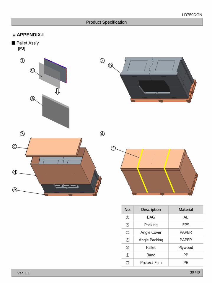
# APPENDIX-I
Pallet Ass’y
[PJ]
① ②
③ ④
No. Description Material
BAG AL
Packing EPS
Angle Cover PAPER
Angle Packing PAPER
Pallet Plywood
Band PP
Protect Film PE
30 /40
Product Specification
LD750DGN
Ver. 1.1
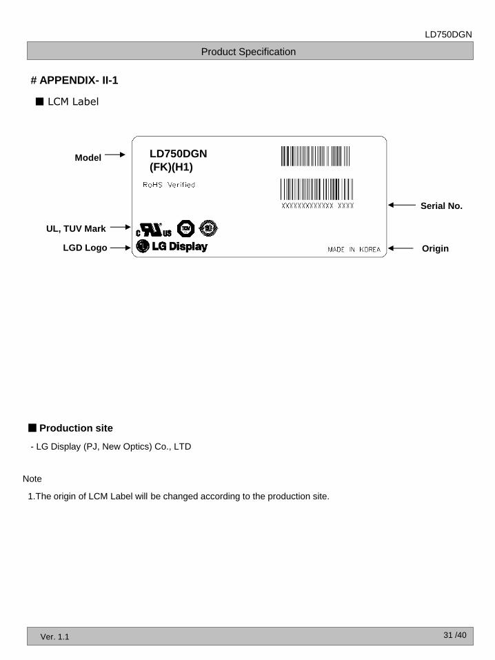
LCM Label
# APPENDIX- II-1
31 /40
Production site
- LG Display (PJ, New Optics) Co., LTD
1.The origin of LCM Label will be changed according to the production site.
Model
Serial No.
UL, TUV Mark
LGD Logo Origin
LD750DGN
(FK)(H1)
Note
Product Specification
LD750DGN
Ver. 1.1
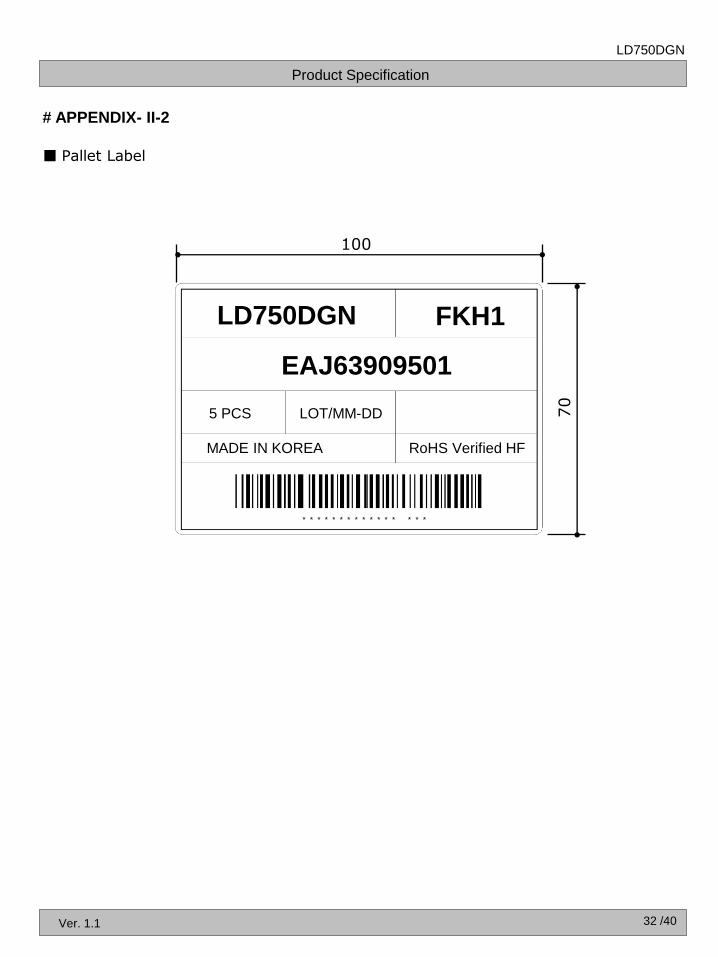
# APPENDIX- II-2
Pallet Label
32 /40
LOT/MM-DD
MADE IN KOREA
* * * * * * * * * * * * * * * *
5 PCS
RoHS Verified HF
LD750DGN FKH1
EAJ63909501
100
70
Product Specification
LD750DGN
Ver. 1.1
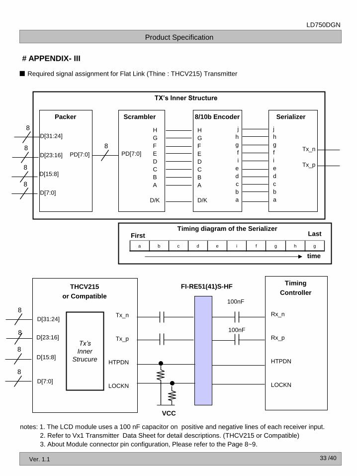
# APPENDIX- III
Required signal assignment for Flat Link (Thine : THCV215) Transmitter
notes: 1. The LCD module uses a 100 nF capacitor on positive and negative lines of each receiver input.
2. Refer to Vx1 Transmitter Data Sheet for detail descriptions. (THCV215 or Compatible)
3. About Module connector pin configuration, Please refer to the Page 8~9.
Packer Scrambler 8/10b Encoder Serializer
j
h
g
f
i
e
d
c
b
a
Tx_n
Tx_p
H
G
F
E
D
C
B
A
j
h
g
f
i
e
d
c
b
a D/K
H
G
F
E
D
C
B
A
D/K
PD[7:0]
8
8
8
8
8
D[7:0]
D[15:8]
D[23:16]
D[31:24]
PD[7:0]
THCV215
or Compatible
8
8
8
8
D[7:0]
D[15:8]
D[23:16]
D[31:24] Tx_n
Tx_p
HTPDN
LOCKN
TX’s Inner Structure
Tx’s
Inner
Strucure
Timing
Controller
Rx_n
Rx_p
HTPDN
LOCKN
a b c d e i f g h g
First Last
time
Timing diagram of the Serializer
FI-RE51(41)S-HF
100nF
100nF
VCC
33 /40
Product Specification
LD750DGN
Ver. 1.1 34 /40
# APPENDIX- IV-1
Option Pin Circuit Block Diagram
1) Circuit Block Diagram of Data format Selection pin
System Side
Input mode
(Pin 17)
1KΩ
Data format Select Pin : Pin 15
ASIC
(TCON) 42kΩ
LCM Side
INPUT Mode
2) Circuit Block Diagram of Bit Selection pin
System Side
Bit Select
(Pin 21)
Bit Select Pin : Pin 21
1 KΩ
ASIC
(TCON)
LCM Side
Bit Select
VCC
36 kΩ
Product Specification
LD750DGN
Ver. 1.1
# APPENDIX- IV-2
Option Pin Circuit Block Diagram
35 /40
3) Circuit Block Diagram of L-Dim Enable Selection pin
ASIC
(TCON)
LCM Side
L-DIM _Enable
(Pin 22) L-DIM _Enable
R1
L-Dim Enable Pin : Pin 22
1KΩ
42 kΩ
System Side
R1 ≤ 1KΩ
1kΩ
System Side
R1 ≤ 1kΩ
(0Ω recommand)
FI-RE51S-HF
pin
#23
LCM Side
RGB or M+ operation : Pin 23
4) Circuit Block Diagram of M+ Bypass Selection pin
ASIC
(TCON)
42 kΩ
Product Specification
LD750DGN
Ver. 1.1
# APPENDIX- IV-3
Option Pin Circuit Block Diagram
5) Circuit Block Diagram of HTPDN/ LOCKN Selection pin
ASIC
(TCON)
System Side LCM Side
HTPDN / LOCKN
(Pin 25,26)
1KΩ
HTPDN/LOCKN Pin : Pin 25, Pin26
36 /40
Product Specification
LD750DGN
Ver. 1.1
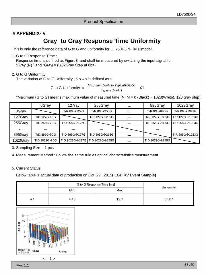
This is only the reference data of G to G and uniformity for LD750DGN-FKH1model.
1. G to G Response Time :
Response time is defined as Figure3 and shall be measured by switching the input signal for
“Gray (N) ” and “Gray(M)”.(32Gray Step at 8bit)
2. G to G Uniformity
The variation of G to G Uniformity , G to G is defined as :
*Maximum (G to G) means maximum value of measured time (N, M = 0 (Black) ~ 1023(White), 128 gray step).
3. Sampling Size : 1 pcs 4. Measurement Method : Follow the same rule as optical characteristics measurement.
5. Current Status
Below table is actual data of production on Oct. 29. 2015( LGD RV Event Sample)
Gray to Gray Response Time Uniformity
< # 1 >
G to G Uniformity = ≤1
G to G Response Time [ms] Uniformity
Min. Max.
# 1 4.43 12.7 0.587
)(
)()(
GtoGTypical
GtoGTypicalGtoGMaximum
# APPENDIX- V
0Gray 127ray 255Gray … 895Gray 1023Gray
0Gray TrR:0G127G TrR:0G255G … TrR:0G895G TrR:0G1023G
127Gray TrD:127G0G TrR:127G255G … TrR:127G895G TrR:127G1023G
255Gray TrD:255G0G TrD:255G127G … TrR:255G895G TrR:255G1023G
… … … … … …
895Gray TrD:895G0G TrD:895G127G TrD:895G255G … TrR:895G1023G
1023Gray TrD:1023G0G TrD:1023G127G TrD:1023G255G … TrD:1023G895G
37 /40
Product Specification
LD750DGN
Ver. 1.1
input mode of pixel data
# APPENDIX-VI
Lane 1st Data 2nd Data Data#
Lane0 1 9 3833
Lane1 2 10 3834
Lane2 3 11 3835
Lane3 4 12 3836
Lane4 5 13 3837
Lane5 6 14 3838
Lane6 7 15 3839
Lane7 8 16 3840
Lane 1st Data 2nd Data Data#
Lane0 1 5 1917
Lane1 2 6 1918
Lane2 3 7 1919
Lane3 4 8 1920
Lane4 1921 1925 3837
Lane5 1922 1926 3838
Lane6 1923 1927 3839
Lane7 1924 1928 3840
Mode 1 : Non-Division Mode 2 : 2 Division
38 /40
Product Specification
LD750DGN
Ver. 1.1 39 /40
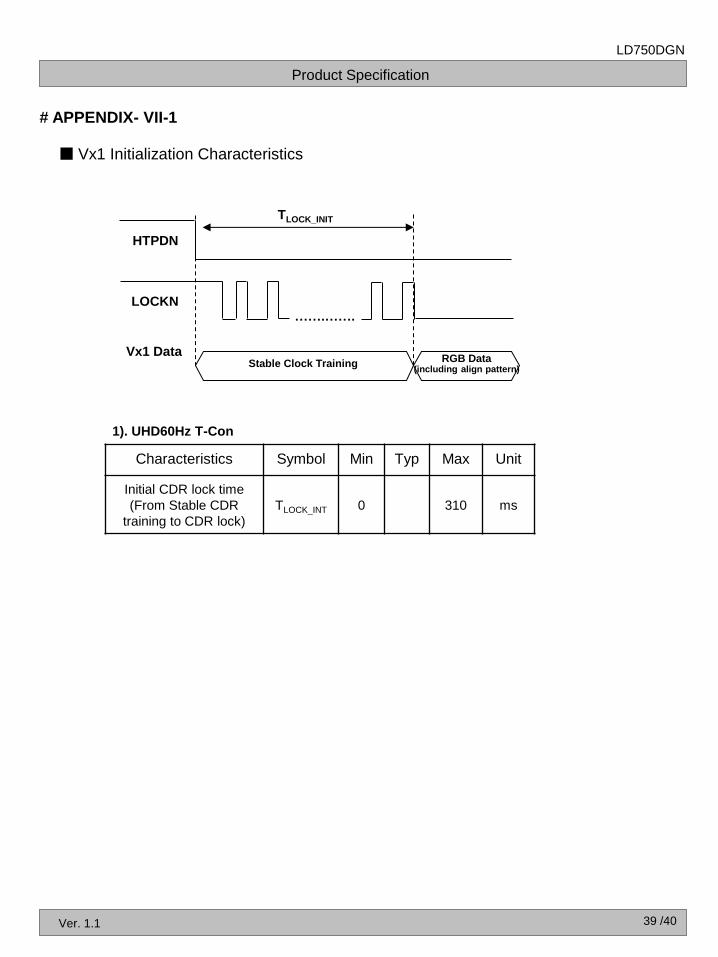
# APPENDIX- VII-1
HTPDN
LOCKN …….…….
Stable Clock Training RGB Data (including align pattern)
Vx1 Data
TLOCK_INIT
Characteristics Symbol Min Typ Max Unit
Initial CDR lock time
(From Stable CDR
training to CDR lock)
TLOCK_INT
0
310
ms
1). UHD60Hz T-Con
Vx1 Initialization Characteristics
Product Specification
LD750DGN
Ver. 1.1 40 /40
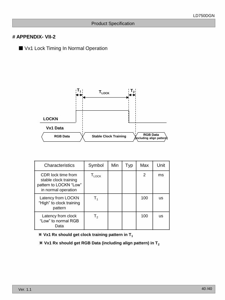
# APPENDIX- VII-2
LOCKN
Stable Clock Training RGB Data (including align pattern)
Vx1 Data
TLOCK
Characteristics Symbol Min Typ Max Unit
CDR lock time from
stable clock training
pattern to LOCKN “Low”
in normal operation
TLOCK 2 ms
Latency from LOCKN
“High” to clock training
pattern
T1 100 us
Latency from clock
“Low” to normal RGB
Data
T2 100 us
RGB Data
T1 T2
※ Vx1 Rx should get clock training pattern in T1
※ Vx1 Rx should get RGB Data (including align pattern) in T2
Vx1 Lock Timing In Normal Operation
Related Documents