University of the East 2219 C.M. Recto Ave., Sampaloc, Manila College of Engineering Electronics Engineering Department NCP 323 – ECE2A (Logic Circuits and Switching Theory Lab) Experiment No. #2 Simplification of Boolean Functions Celestre, John Donnie I. Gregorio, Hasley R. Guevarra, Christian Paul Medina, Marbie Gerald G. Roxas, Rowell N. Fernando Victor V. de Vera, RECE, M.Tech Instructor Date of Performance: 06 January 2014 Date of Submission: 13 January 2014

Welcome message from author
This document is posted to help you gain knowledge. Please leave a comment to let me know what you think about it! Share it to your friends and learn new things together.
Transcript
University of the East
2219 C.M. Recto Ave., Sampaloc, Manila College of Engineering
Electronics Engineering Department
NCP 323 – ECE2A (Logic Circuits and Switching Theory Lab) Experiment No. #2
Simplification of Boolean Functions
Celestre, John Donnie I.
Gregorio, Hasley R.
Guevarra, Christian Paul
Medina, Marbie Gerald G.
Roxas, Rowell N.
Fernando Victor V. de Vera, RECE, M.Tech Instructor
Date of Performance: 06 January 2014 Date of Submission: 13 January 2014
LCST Laboratory Experiment Experiment 2: Simplification of Boolean Functions
Objectives:
1. To be familiar with Boolean algebra postulates and theories. 2. To prove Boolean algebra postulates and theories by constructing the given and simplified logic circuits and comparing their output.
Theoretical Background A Boolean function describes how to determine a Boolean value output
based on some logical calculation from Boolean inputs. Such functions play a basic role in questions of complexity theory as well as the design of circuits and chips for digital computers. The properties of Boolean functions play a critical role in cryptography, particularly in the design of symmetric key algorithms. A Boolean function can be simplified using “Boolean Algebra”.
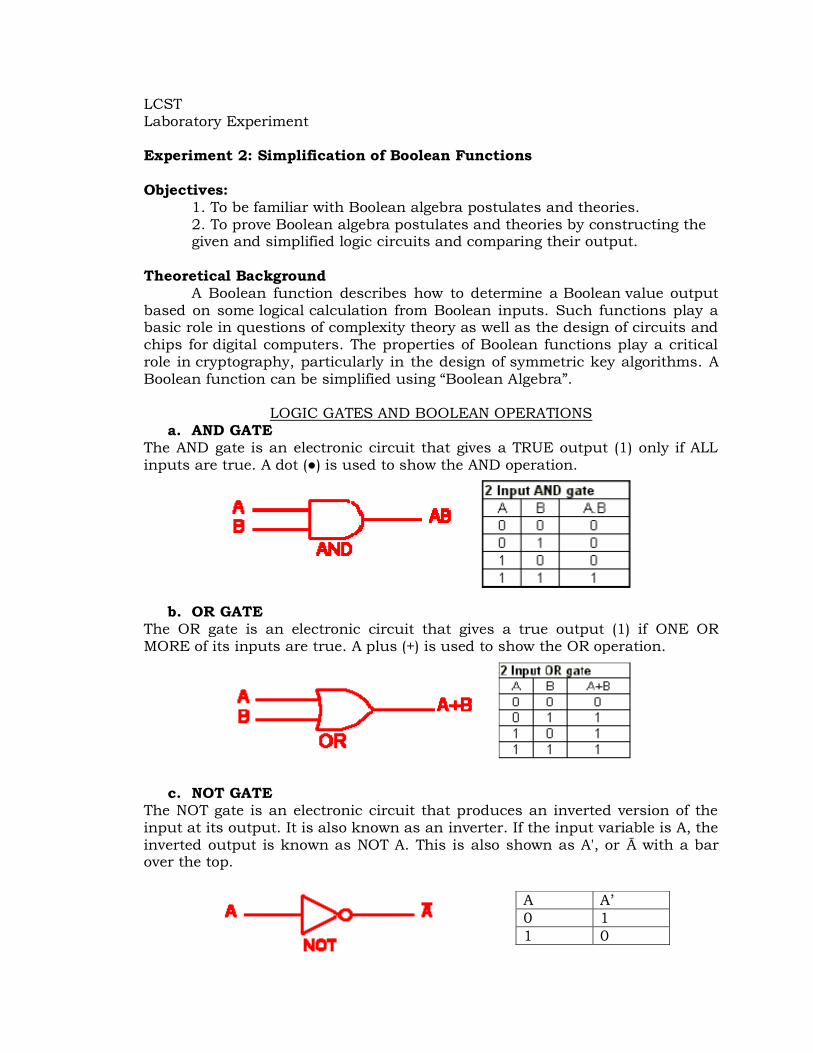
LOGIC GATES AND BOOLEAN OPERATIONS
a. AND GATE The AND gate is an electronic circuit that gives a TRUE output (1) only if ALL inputs are true. A dot (●) is used to show the AND operation.
b. OR GATE
The OR gate is an electronic circuit that gives a true output (1) if ONE OR MORE of its inputs are true. A plus (+) is used to show the OR operation.
c. NOT GATE The NOT gate is an electronic circuit that produces an inverted version of the input at its output. It is also known as an inverter. If the input variable is A, the inverted output is known as NOT A. This is also shown as A', or Ā with a bar over the top.
A A’
0 1
1 0
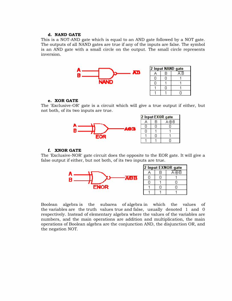
d. NAND GATE
This is a NOT-AND gate which is equal to an AND gate followed by a NOT gate. The outputs of all NAND gates are true if any of the inputs are false. The symbol
is an AND gate with a small circle on the output. The small circle represents inversion.
e. XOR GATE
The 'Exclusive-OR' gate is a circuit which will give a true output if either, but
not both, of its two inputs are true.
f. XNOR GATE
The 'Exclusive-NOR' gate circuit does the opposite to the EOR gate. It will give a false output if either, but not both, of its two inputs are true.
Boolean algebra is the subarea of algebra in which the values of
the variables are the truth values true and false, usually denoted 1 and 0 respectively. Instead of elementary algebra where the values of the variables are numbers, and the main operations are addition and multiplication, the main operations of Boolean algebra are the conjunction AND, the disjunction OR, and the negation NOT.
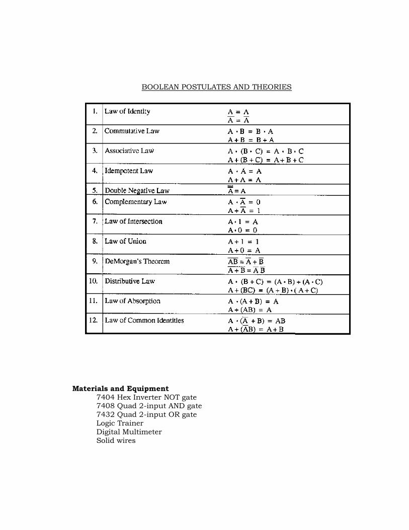
BOOLEAN POSTULATES AND THEORIES
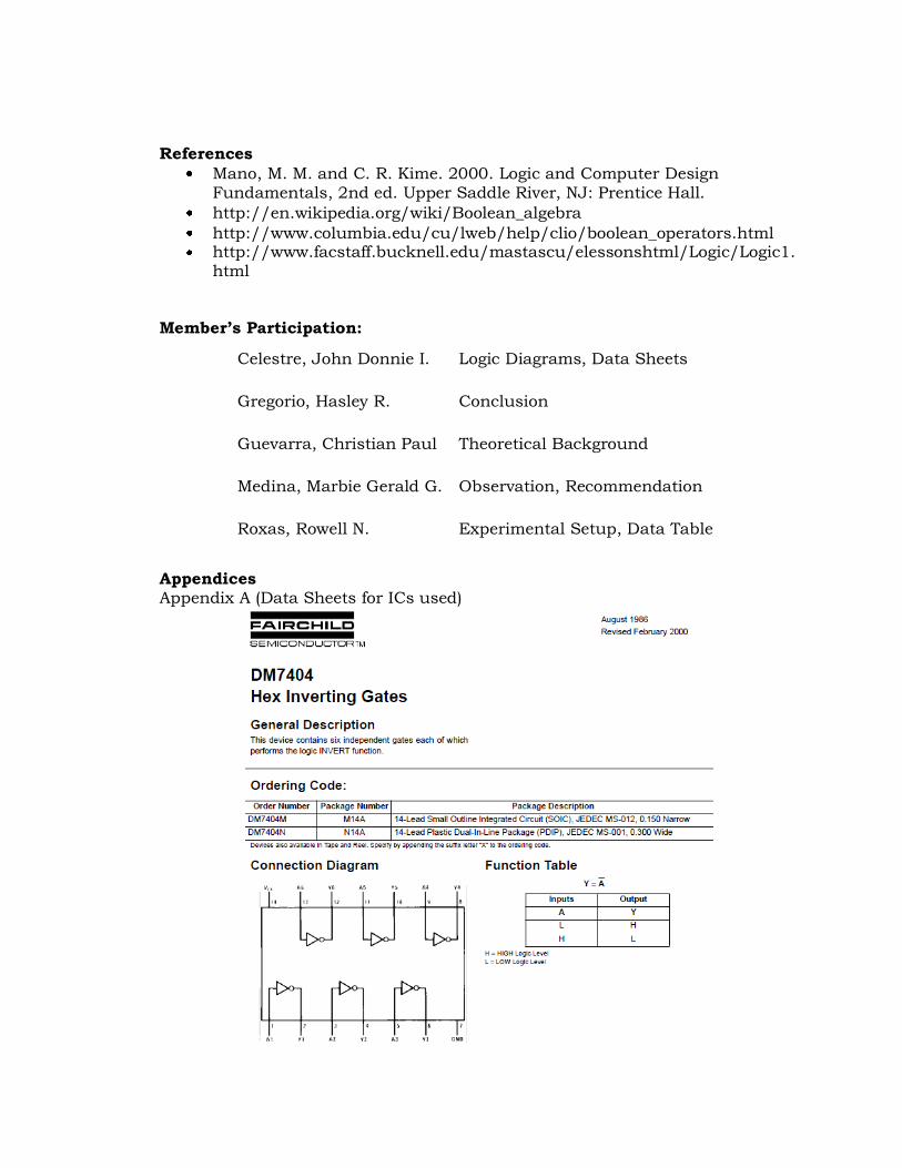
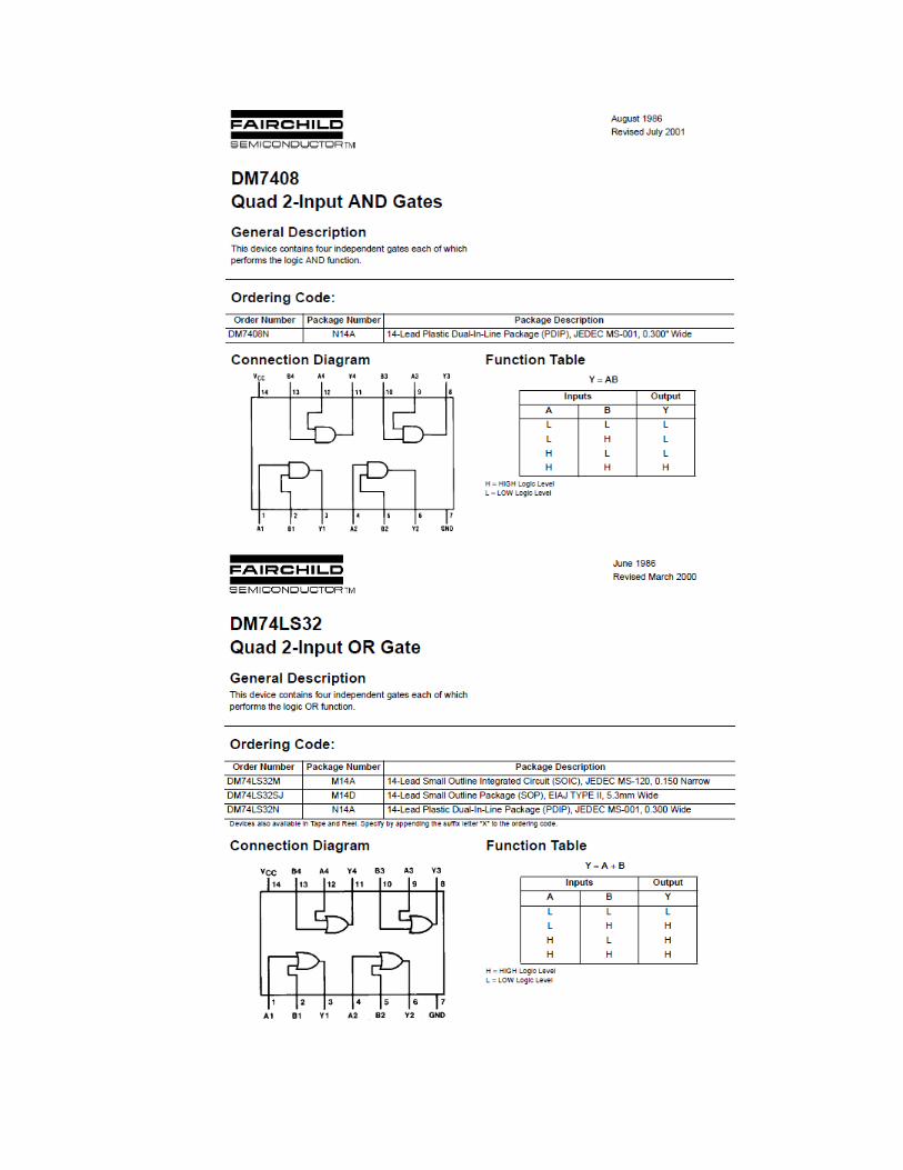
Materials and Equipment 7404 Hex Inverter NOT gate 7408 Quad 2-input AND gate 7432 Quad 2-input OR gate Logic Trainer Digital Multimeter Solid wires
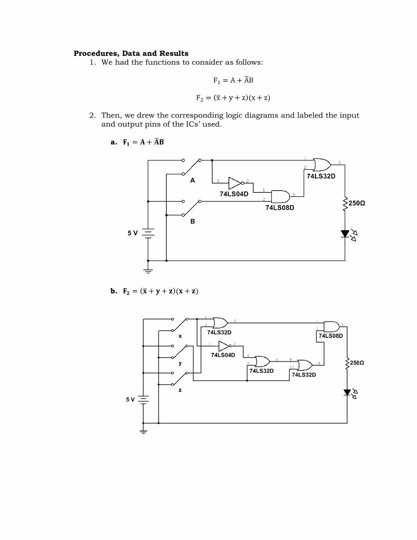
Procedures, Data and Results 1. We had the functions to consider as follows:
2. Then, we drew the corresponding logic diagrams and labeled the input and output pins of the ICs’ used.
a.
b.
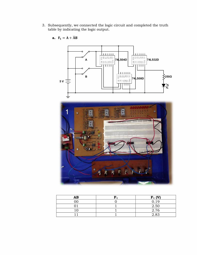
3. Subsequently, we connected the logic circuit and completed the truth table by indicating the logic output.
a.
AB F1 F1 (V)
00 0 0.19
01 1 2.50
10 1 2.76
11 1 2.83
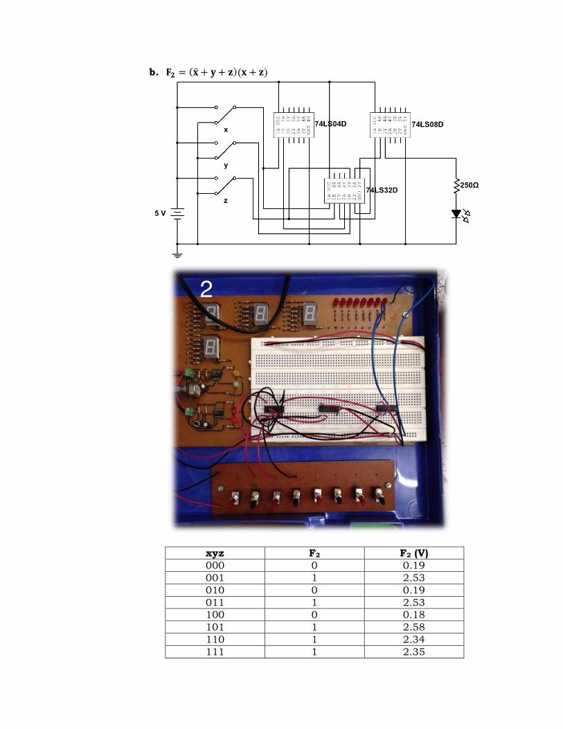
b.
xyz F2 F2 (V)
000 0 0.19
001 1 2.53
010 0 0.19
011 1 2.53
100 0 0.18
101 1 2.58
110 1 2.34
111 1 2.35
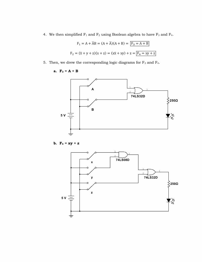
4. We then simplified F1 and F2 using Boolean algebra to have F3 and F4.
5. Then, we drew the corresponding logic diagrams for F3 and F4.
a. F3 = A + B
b. F4 = xy + z
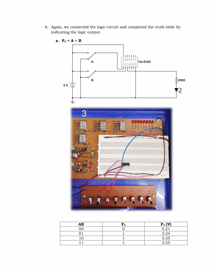
6. Again, we connected the logic circuit and completed the truth table by
indicating the logic output.
a. F3 = A + B
AB F3 F3 (V)
00 0 0.21
01 1 3.24
10 1 3.25
11 1 3.25
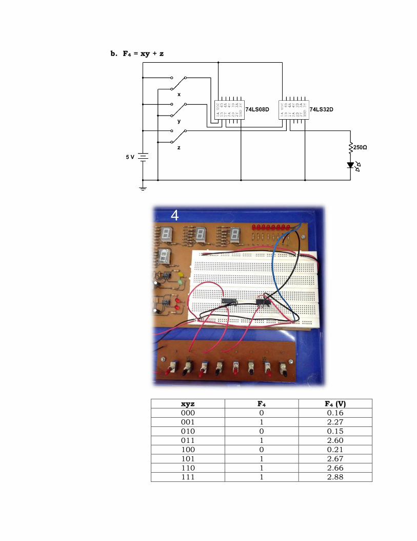
b. F4 = xy + z
xyz F4 F4 (V)
000 0 0.16
001 1 2.27
010 0 0.15
011 1 2.60
100 0 0.21
101 1 2.67
110 1 2.66
111 1 2.88
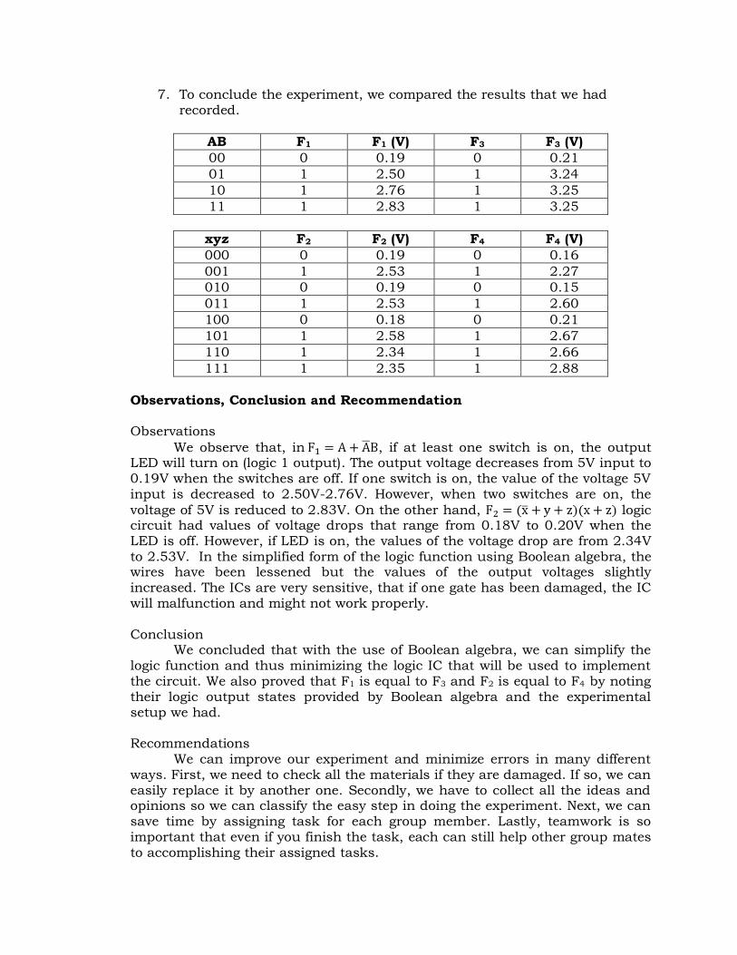
7. To conclude the experiment, we compared the results that we had recorded.
AB F1 F1 (V) F3 F3 (V)
00 0 0.19 0 0.21
01 1 2.50 1 3.24
10 1 2.76 1 3.25
11 1 2.83 1 3.25
xyz F2 F2 (V) F4 F4 (V)
000 0 0.19 0 0.16
001 1 2.53 1 2.27
010 0 0.19 0 0.15
011 1 2.53 1 2.60
100 0 0.18 0 0.21
101 1 2.58 1 2.67
110 1 2.34 1 2.66
111 1 2.35 1 2.88
Observations, Conclusion and Recommendation Observations
We observe that, in , if at least one switch is on, the output LED will turn on (logic 1 output). The output voltage decreases from 5V input to 0.19V when the switches are off. If one switch is on, the value of the voltage 5V input is decreased to 2.50V-2.76V. However, when two switches are on, the
voltage of 5V is reduced to 2.83V. On the other hand, logic circuit had values of voltage drops that range from 0.18V to 0.20V when the LED is off. However, if LED is on, the values of the voltage drop are from 2.34V to 2.53V. In the simplified form of the logic function using Boolean algebra, the wires have been lessened but the values of the output voltages slightly increased. The ICs are very sensitive, that if one gate has been damaged, the IC will malfunction and might not work properly. Conclusion We concluded that with the use of Boolean algebra, we can simplify the
logic function and thus minimizing the logic IC that will be used to implement the circuit. We also proved that F1 is equal to F3 and F2 is equal to F4 by noting their logic output states provided by Boolean algebra and the experimental setup we had. Recommendations We can improve our experiment and minimize errors in many different ways. First, we need to check all the materials if they are damaged. If so, we can easily replace it by another one. Secondly, we have to collect all the ideas and opinions so we can classify the easy step in doing the experiment. Next, we can save time by assigning task for each group member. Lastly, teamwork is so important that even if you finish the task, each can still help other group mates to accomplishing their assigned tasks.
References
Mano, M. M. and C. R. Kime. 2000. Logic and Computer Design
Fundamentals, 2nd ed. Upper Saddle River, NJ: Prentice Hall.
http://en.wikipedia.org/wiki/Boolean_algebra
http://www.columbia.edu/cu/lweb/help/clio/boolean_operators.html http://www.facstaff.bucknell.edu/mastascu/elessonshtml/Logic/Logic1.
html Member’s Participation:
Celestre, John Donnie I. Logic Diagrams, Data Sheets
Gregorio, Hasley R. Conclusion
Guevarra, Christian Paul Theoretical Background
Medina, Marbie Gerald G. Observation, Recommendation
Roxas, Rowell N. Experimental Setup, Data Table
Appendices Appendix A (Data Sheets for ICs used)
Appendix B (Boolean Postulates and Theories)
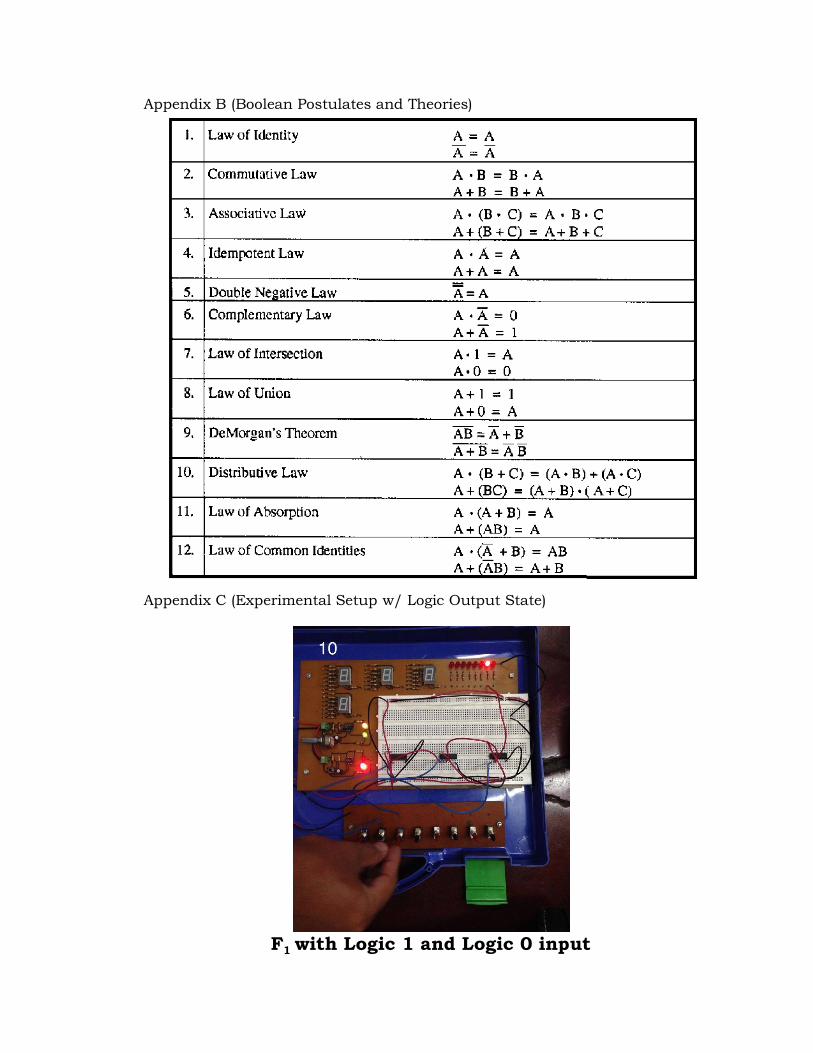
Appendix C (Experimental Setup w/ Logic Output State)
F1 with Logic 1 and Logic 0 input
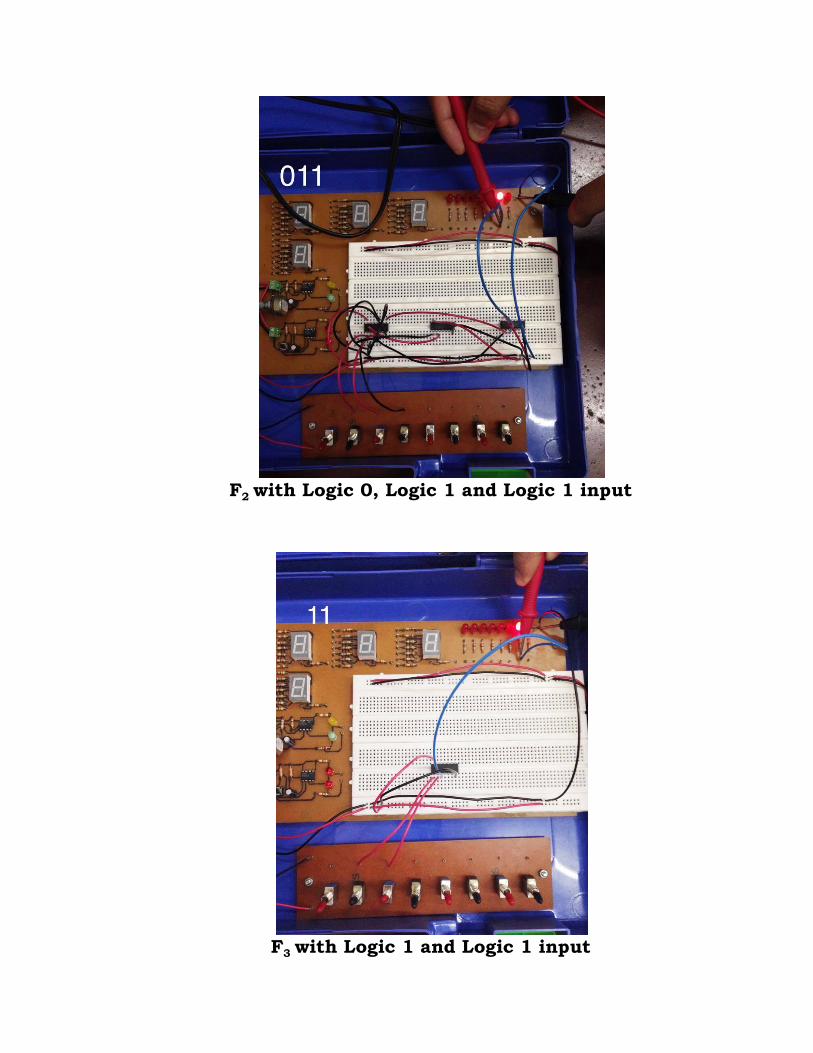
F2 with Logic 0, Logic 1 and Logic 1 input
F3 with Logic 1 and Logic 1 input
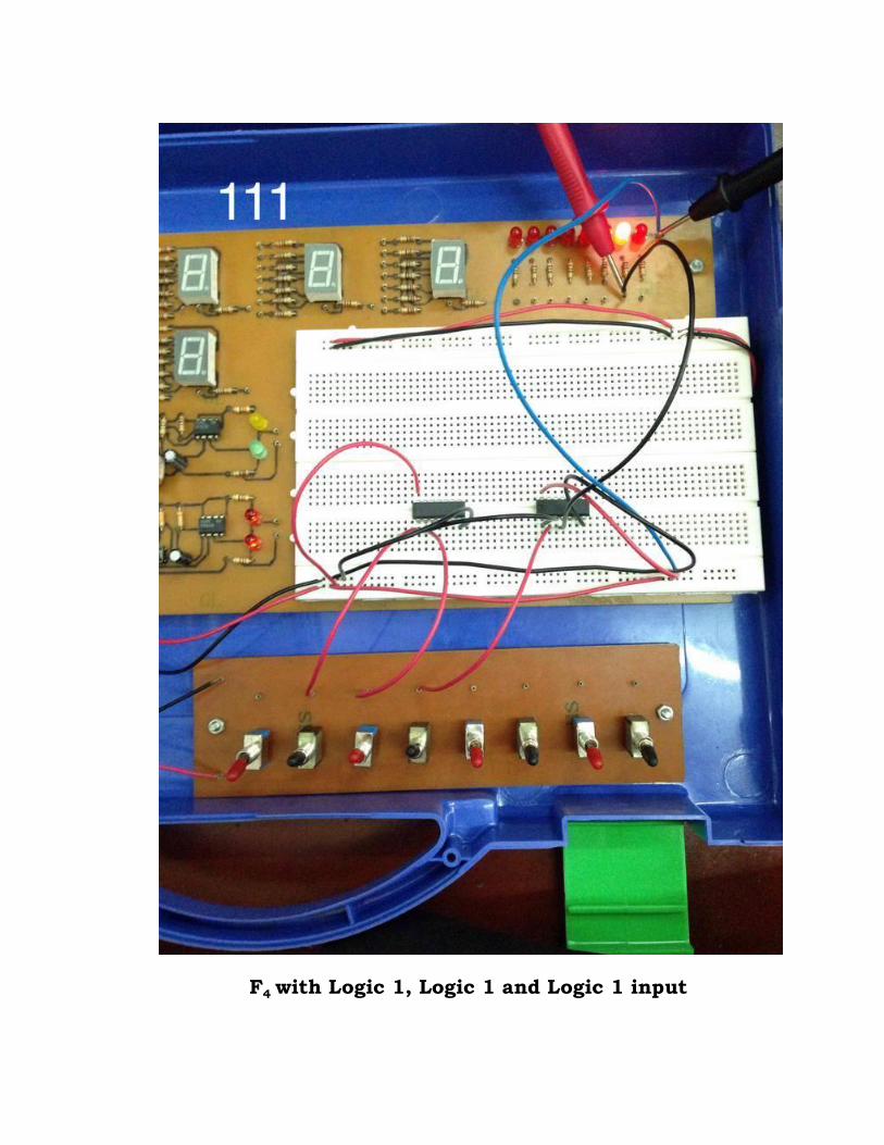
F4 with Logic 1, Logic 1 and Logic 1 input
Related Documents