Layer 0 Grounding • Requirement in terms of noise performance • Grounding/Shielding studies with L0 prototype • Summary Kazu Hanagaki / Fermilab

Layer 0 Grounding Requirement in terms of noise performance Grounding/Shielding studies with L0 prototype Summary Kazu Hanagaki / Fermilab.
Dec 17, 2015
Welcome message from author
This document is posted to help you gain knowledge. Please leave a comment to let me know what you think about it! Share it to your friends and learn new things together.
Transcript

Layer 0 Grounding
• Requirement in terms of noise performance
• Grounding/Shielding studies with L0 prototype
• Summary
Kazu Hanagaki / Fermilab
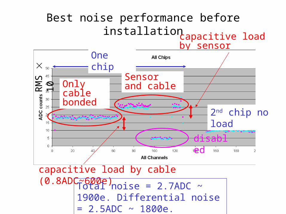
Best noise performance before installationcapacitive load by sensor (0.7ADC~500e)
capacitive load by cable (0.8ADC~600e)
2nd chip no load
One chip
RM
S
10
Only cable bonded
Sensor and cable
disabled
Total noise = 2.7ADC ~ 1900e. Differential noise = 2.5ADC ~ 1800e.
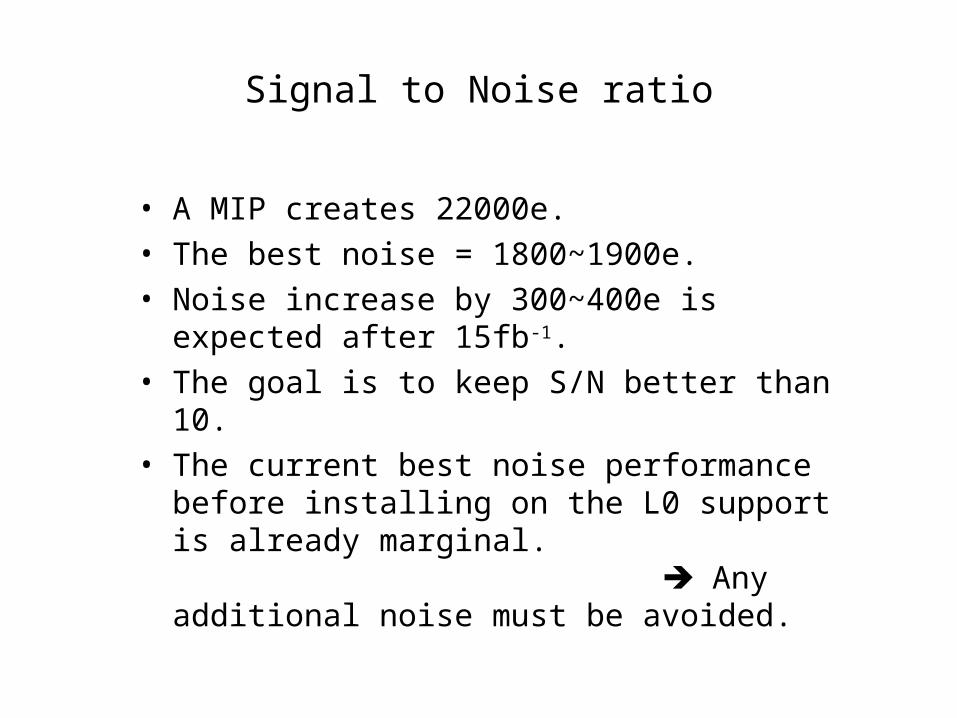
Signal to Noise ratio
• A MIP creates 22000e.
• The best noise = 1800~1900e.
• Noise increase by 300~400e is expected after 15fb-1.
• The goal is to keep S/N better than 10.
• The current best noise performance before installing on the L0 support is already marginal. Any additional noise must be avoided.

L0 prototype module

Grounding Studies
sensor SVX4/hybrid
Metal box
L0 support
Kapton flex
Analog cable GND(20)
GNDhybrid GNDsensor GND
Signal return
Signal ground
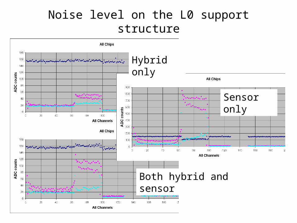
Noise level on the L0 support structure
Hybrid only
Sensor only
Both hybrid and sensor
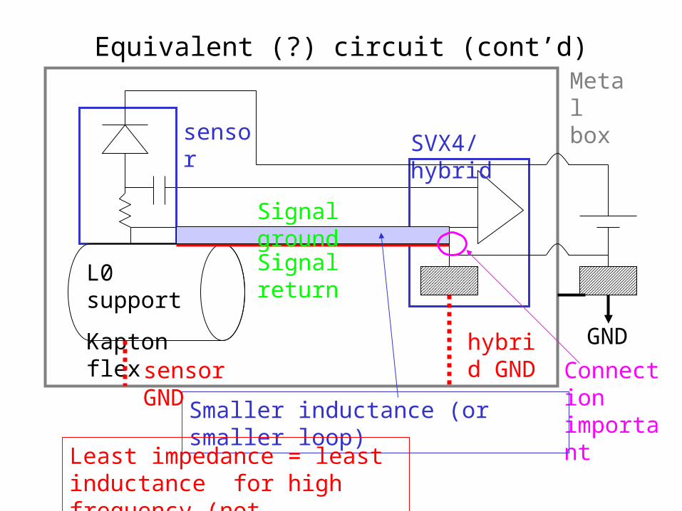
Equivalent (?) circuit (cont’d)
Connection important
sensor SVX4/hybrid
Metal box
L0 support
Kapton flexGNDhybrid
GNDsensor GND
Signal return
Signal ground
Smaller inductance (or smaller loop)
Least impedance = least inductance for high frequency (not resistance).

After putting extra grounding planeNote! Still the hybrid grounding is not perfect in terms of getting low inductance… but the effect of the extra grounding by kapton flex is so clear!!!
Single ground at hybrid
Common ground at both hybrid and sensor

Importance of low inductance connection
1 wire between hybrid and the extra grounding plane
3 wires 4 wires
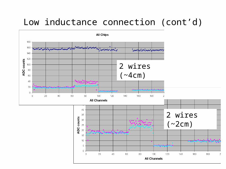
Low inductance connection (cont’d)
2 wires (~2cm)
2 wires (~4cm)

Reducing the inductance
• Having lower inductance connection to GND seems crucial.
• L ~ (wire) length/radius: M=l/2[log(2l/r)-1]
• L = /I
• ~ area of the closed circuit
• People know these rules well, but sometimes forget to apply.
• But these rules are always critical for any grounding connections, both locally and generally.
better
Carbon Fiber
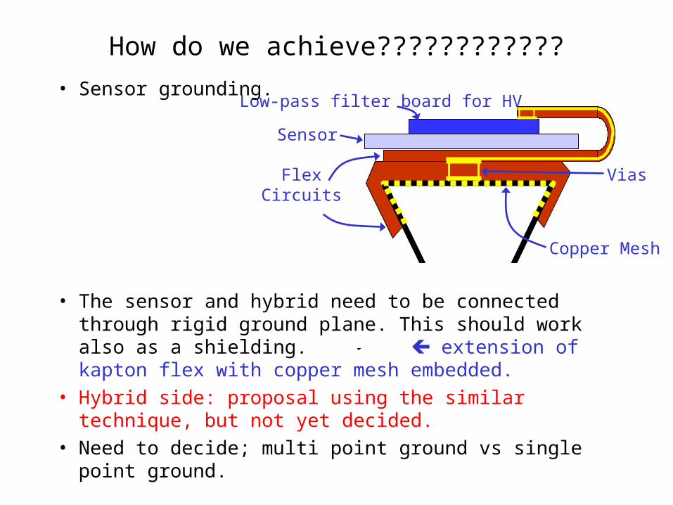
FlexCircuits
Vias
Low-pass filter board for HV
Sensor
Copper Mesh
How do we achieve????????????
• Sensor grounding.
• The sensor and hybrid need to be connected through rigid ground plane. This should work also as a shielding. extension of kapton flex with copper mesh embedded.
• Hybrid side: proposal using the similar technique, but not yet decided.
• Need to decide; multi point ground vs single point ground.

Summary
• No additional noise is allowed for L0.
• Low inductance ground connection is crucial, especially at the hybrid end.
• Grounding scheme at the hybrid must be fixed.
• Rigid grounding, or low inductance grounding path to the outside world must be maintained.

…Backup Slides

Signal to Noise ratio
S/N=10
CSi Ccable
Total noise estimates VS total capacitance
Noise increase by 300~400e is expected after the irradiation.
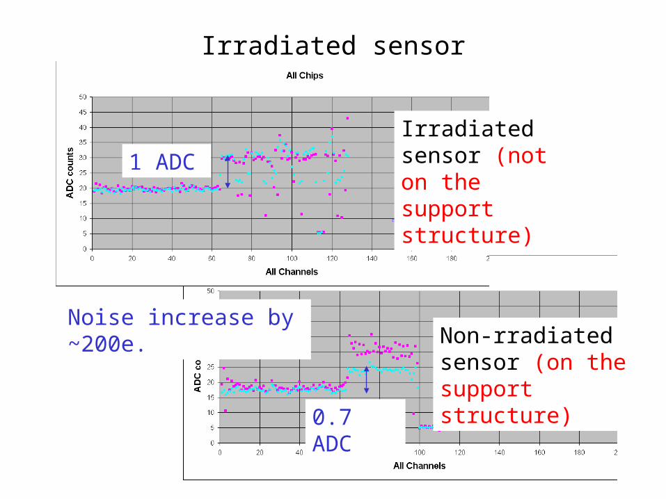
Irradiated sensor
Irradiated sensor (not on the support structure)
Non-rradiated sensor (on the support structure)
Noise increase by ~200e.
1 ADC
0.7 ADC
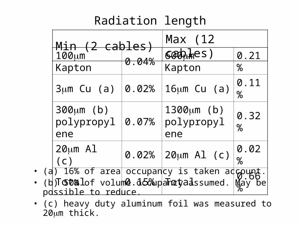
Radiation length
• (a) 16% of area occupancy is taken account.• (b) 50% of volume occupancy assumed. May be possible
to reduce.• (c) heavy duty aluminum foil was measured to 20m thick.
100m Kapton 0.04% 600m Kapton 0.21%
3m Cu (a) 0.02% 16m Cu (a) 0.11%
300m (b) polypropylene
0.07%1300m (b) polypropylene
0.32%
20m Al (c) 0.02% 20m Al (c) 0.02%
Total 0.15% Total 0.66%
Min (2 cables) Max (12 cables)

Cable design
sensor
cablespacer
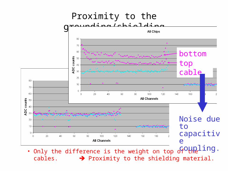
Proximity to the grounding/shielding
• Only the difference is the weight on top of the cables. Proximity to the shielding material.
bottom cabletop cable
Noise due to capacitive coupling.
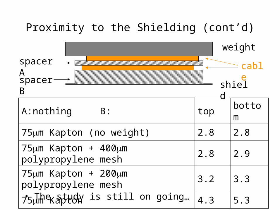
Proximity to the Shielding (cont’d)
• The study is still on going…
cablespacer A
spacer B shield
weight
A:nothing B: top bottom
75m Kapton (no weight) 2.8 2.8
75m Kapton + 400m polypropylene mesh 2.8 2.9
75m Kapton + 200m polypropylene mesh 3.2 3.3
75m Kapton 4.3 5.3

Choice of spacer
• Dyconex has produced three different meshes with kapton sheet.– hole radius: 60 m– hole-distance: 190, 210 and 230 m– corresponding to r ~1.95, 2.2 and 2.45
• Polypropylene mesh sheet
190 m 210 m 230 m
Related Documents