Lateral resolution in focused electron beam-induced deposition: scaling laws for pulsed and static exposure Aleksandra Szkudlarek • Wojciech Szmyt • Czeslaw Kapusta • Ivo Utke Received: 4 April 2014 / Accepted: 27 August 2014 / Published online: 18 September 2014 Ó The Author(s) 2014. This article is published with open access at Springerlink.com Abstract In this work, we review the single-adsorbate time-dependent continuum model for focused electron beam-induced deposition (FEBID). The differential equa- tion for the adsorption rate will be expressed by dimen- sionless parameters describing the contributions of adsorption, desorption, dissociation, and the surface diffu- sion of the precursor adsorbates. The contributions are individually presented in order to elucidate their influence during variations in the electron beam exposure time. The findings are condensed into three new scaling laws for pulsed exposure FEBID (or FEB-induced etching) relating the lateral resolution of deposits or etch pits to surface diffusion and electron beam exposure dwell time for a given adsorbate depletion state. 1 Introduction Focused electron beam-induced deposition (FEBID) is a maskless direct-write nanolithography technique, in which the precursor gas molecules are directly delivered into the electron microscope chamber, where they are adsorbed onto the substrate surface and dissociated via the interac- tion with the focused electron beam [1]. In such a way, local functional nanostructures can be formed without multistep processing, which is necessary in common resist- based electron beam lithography. Among the functional materials that have been fabricated using FEBID are fer- romagnetic wires [2–4], metallic [5], and graphitic material [6] for low-resistance nanocontacts, as well as granular wires for strain sensors [7], magnetic sensors [8], gas sensors [9], and material with photonic/plasmonic func- tionality [10–13]. Although the above-sketched concept of FEBID seems to be simple, the final product depends on the three types of interactions: electron beam—substrate, electron beam— adsorbates, and adsorbates—substrates. The interaction between electron beam and adsorbates involves already several parameters related to the adsorbate surface kinetics and their dissociation efficiency by the electron beam. As a result, already for the simple case of stationary electron beam (spot) exposures, various types of deposit shape profiles can be obtained, see (Fig. 1). These shape profiles were well described by the FEBID continuum model [14– 16]. When the electron beam-dissociated adsorbates are instantaneously replenished by new adsorbates or incoming molecules, the deposit shape corresponds to the Gaussian profile of the beam and the process is carried out in the electron-limited regime (Fig. 1a). Should the adsorbates be depleted inside the irradiated area, the surface diffusion of adsorbates from the surrounding non-irradiated area starts to play a considerable role. A characteristic indent shape is often obtained for the diffusion-enhanced regime (Fig. 1b) as adsorbates diffusing to the center of the irradiated area are dissociated at its rim by the electron beam tails. If Electronic supplementary material The online version of this article (doi:10.1007/s00339-014-8751-2) contains supplementary material, which is available to authorized users. A. Szkudlarek (&) I. Utke Laboratory for Mechanics of Materials and Nanostructures, Empa, Feuerwerkerstrasse 39, 3602 Thun, Switzerland e-mail: [email protected] I. Utke e-mail: [email protected] A. Szkudlarek W. Szmyt C. Kapusta Department of Solid State Physics, Faculty of Physics and Applied Computer Science, AGH University of Science and Technology, al. A. Mickiewicza 30, 30-059 Krako ´w, Poland 123 Appl. Phys. A (2014) 117:1715–1726 DOI 10.1007/s00339-014-8751-2

Welcome message from author
This document is posted to help you gain knowledge. Please leave a comment to let me know what you think about it! Share it to your friends and learn new things together.
Transcript
Lateral resolution in focused electron beam-induced deposition:scaling laws for pulsed and static exposure
Aleksandra Szkudlarek • Wojciech Szmyt •
Czesław Kapusta • Ivo Utke
Received: 4 April 2014 / Accepted: 27 August 2014 / Published online: 18 September 2014
� The Author(s) 2014. This article is published with open access at Springerlink.com
Abstract In this work, we review the single-adsorbate
time-dependent continuum model for focused electron
beam-induced deposition (FEBID). The differential equa-
tion for the adsorption rate will be expressed by dimen-
sionless parameters describing the contributions of
adsorption, desorption, dissociation, and the surface diffu-
sion of the precursor adsorbates. The contributions are
individually presented in order to elucidate their influence
during variations in the electron beam exposure time. The
findings are condensed into three new scaling laws for
pulsed exposure FEBID (or FEB-induced etching) relating
the lateral resolution of deposits or etch pits to surface
diffusion and electron beam exposure dwell time for a
given adsorbate depletion state.
1 Introduction
Focused electron beam-induced deposition (FEBID) is a
maskless direct-write nanolithography technique, in which
the precursor gas molecules are directly delivered into the
electron microscope chamber, where they are adsorbed
onto the substrate surface and dissociated via the interac-
tion with the focused electron beam [1]. In such a way,
local functional nanostructures can be formed without
multistep processing, which is necessary in common resist-
based electron beam lithography. Among the functional
materials that have been fabricated using FEBID are fer-
romagnetic wires [2–4], metallic [5], and graphitic material
[6] for low-resistance nanocontacts, as well as granular
wires for strain sensors [7], magnetic sensors [8], gas
sensors [9], and material with photonic/plasmonic func-
tionality [10–13].
Although the above-sketched concept of FEBID seems
to be simple, the final product depends on the three types of
interactions: electron beam—substrate, electron beam—
adsorbates, and adsorbates—substrates. The interaction
between electron beam and adsorbates involves already
several parameters related to the adsorbate surface kinetics
and their dissociation efficiency by the electron beam. As a
result, already for the simple case of stationary electron
beam (spot) exposures, various types of deposit shape
profiles can be obtained, see (Fig. 1). These shape profiles
were well described by the FEBID continuum model [14–
16]. When the electron beam-dissociated adsorbates are
instantaneously replenished by new adsorbates or incoming
molecules, the deposit shape corresponds to the Gaussian
profile of the beam and the process is carried out in the
electron-limited regime (Fig. 1a). Should the adsorbates be
depleted inside the irradiated area, the surface diffusion of
adsorbates from the surrounding non-irradiated area starts
to play a considerable role. A characteristic indent shape is
often obtained for the diffusion-enhanced regime (Fig. 1b)
as adsorbates diffusing to the center of the irradiated area
are dissociated at its rim by the electron beam tails. If
Electronic supplementary material The online version of thisarticle (doi:10.1007/s00339-014-8751-2) contains supplementarymaterial, which is available to authorized users.
A. Szkudlarek (&) � I. Utke
Laboratory for Mechanics of Materials and Nanostructures,
Empa, Feuerwerkerstrasse 39, 3602 Thun, Switzerland
e-mail: [email protected]
I. Utke
e-mail: [email protected]
A. Szkudlarek � W. Szmyt � C. Kapusta
Department of Solid State Physics, Faculty of Physics and
Applied Computer Science, AGH University of Science and
Technology, al. A. Mickiewicza 30, 30-059 Krakow, Poland
123
Appl. Phys. A (2014) 117:1715–1726
DOI 10.1007/s00339-014-8751-2
surface diffusion is strong, the adsorbates can reach the
center and a round-shaped deposit is obtained (Fig. 1d). In
the last case, in the adsorbate-limited regime when the
depletion rate is larger than the adsorbate replenishment
and when the surface diffusion is weak, the flattop deposit
shape is observed (Fig. 1c).
2 Continuum model
The continuum model for stationary FEBID was previously
described in detail in [15, 16]. Here, we propose a general
approach, referring to the time-dependent version of the
adsorption rate equation with a set of two independent
parameters, which describe the adsorbate surface diffusion
and the irradiative depletion. This methodology can be
applied to focused electron beam-induced deposition and
etching to obtain the shapes of the deposit or the respective
etch pit. The solution of the stationary-state adsorption rate
equation using this methodology has already been discussed
in [16]. Several precursor-specific approaches were reported
in the literature: the fundamental interactions between the
beam and adsorbate in pulsed FEBID are discussed in [17],
taking W(CO)6 as a gas precursor. Experimental etch shapes
using XeF2 as a precursor gas have been correlated with the
process parameters in [18, 19]. A transition between
simultaneous etching and deposition of the contamination
deposit was discussed in [20]. The continuum model, which
explains this effect including two types of adsorbates spe-
cies—one etching and another one forming a deposit—was
developed in [21]. Simultaneous co-adsorption of two
precursor gases for deposition without taking surface dif-
fusion into account was studied in [22, 23]. Specific phe-
nomena which may appear during the FEBID process, like
chemisorption or electron-stimulated desorption of adsor-
bates, were proposed in [24] and [25], respectively.
In the following, we want to discuss more generally the
evolution of the individual contributions of adsorption,
desorption, irradiative depletion, and surface diffusion with
electron beam exposure time in order to derive scaling laws
for the lateral resolution in deposition and etching with
focused electron beams.
3 Concentration of adsorbates—surface coverage
The local number n of adsorbates at a given area on the
surface can change due to the four following processes,
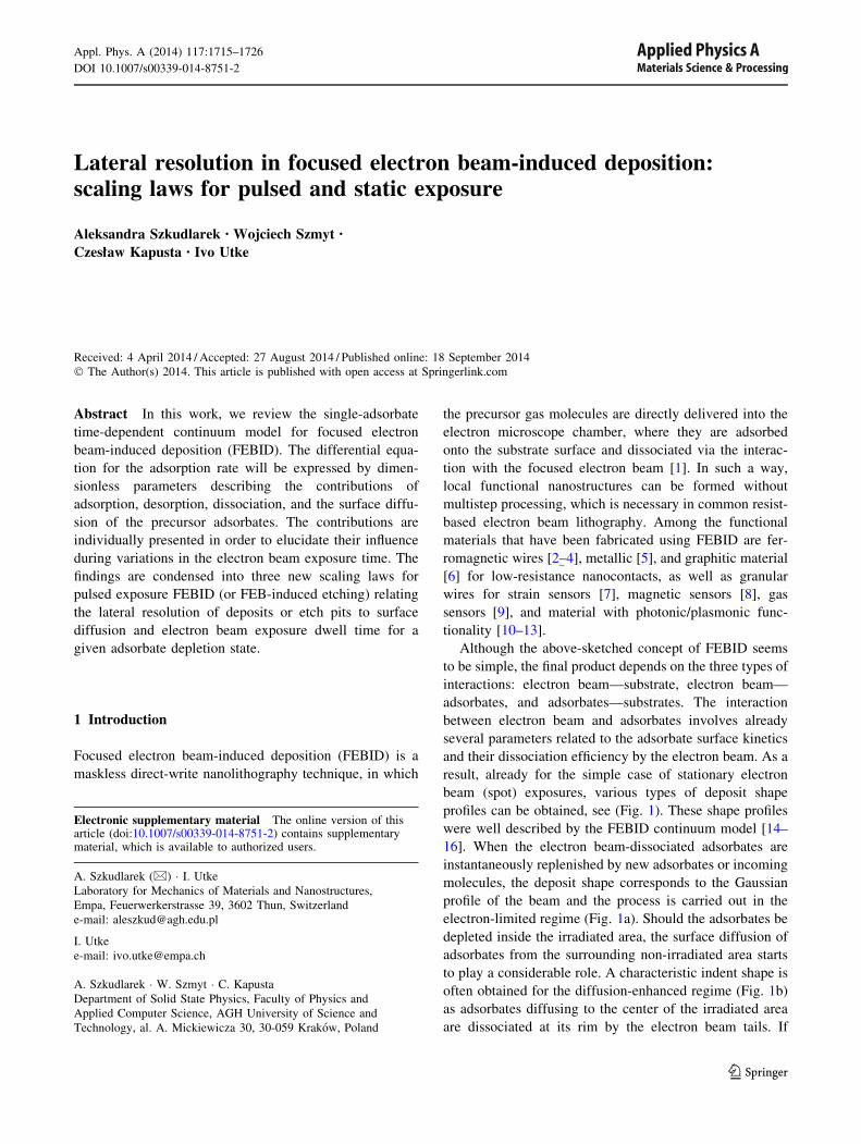
which are schematically presented in Fig. 2:
• adsorption, which is proportional to the impinging rate
of precursor gas molecules J and to the number of
available places 1� nn0
� �with n0 the adsorbates
concentration of a complete monolayer; as there is no
condensation process occurring, n0 represents the
maximum value for n
• desorption, where the physisorbed molecules have a
given average residence time s, after that they sponta-
neously desorb thermally from the surface
• dissociation, the rate of which is proportional to the
electron flux f ðrÞ and the number of available adsorbates
Fig. 1 Deposit shapes and
process regimes for stationary
single-spot exposures with a
Gaussian profile electron beam.
The generic shapes correspond
to the process regimes:
a Gaussian shape for electron-
limited regime (also known as
reaction rate-limited regime),
b Indent shape for diffusion-
enhanced regime, c Flattop
shape for adsorbate-limited
regime (also known as mass
transport-limited regime),
d Rounded shape for a mixed
diffusion-enhanced/adsorbate-
limited regime
1716 A. Szkudlarek et al.
123
with a constant r ¼ r EBð Þ called a net dissociation cross
section, depending on the beam energy EB and the
chemical composition of the adsorbate
• surface diffusion, which is proportional to the adsorbate
diffusivity described by the surface diffusion coeffi-
cient D and the Laplacian of adsorbate concentration
r2n ¼ o2nox2 þ o2n
oy2 with r being the Nabla operator. This
expression applies to non-interacting adsorbates and
represents Fick’s law of diffusion.
The adsorption rate equation describing the change in
the local concentration of adsorbates is
Fig. 2 Physicochemical mechanisms in FEBID process: (1) adsorp-
tion—proportional to the sticking probability, impinging molecular
flux, and non-occupied adsorption sites; (2) thermal spontaneous
desorption—inversely proportional to the average residence time
characteristic for a given adsorbate; (3) electron-induced
dissociation—depending on the electron flux, number of adsorbates,
and the efficiency of the electron-induced dissociation reaction
described by the net dissociation cross section; (4) surface diffusion—
being proportional to the divergence of the gradient of adsorbates and
the surface diffusion constant as a proportionality factor
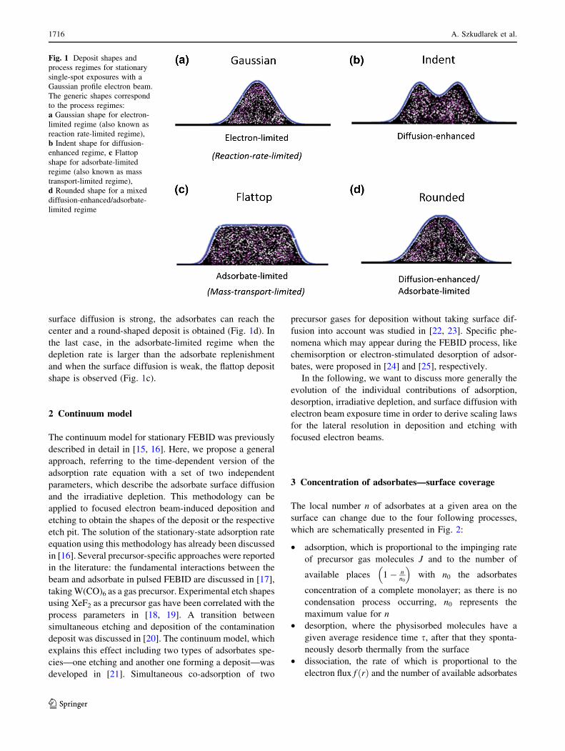
Fig. 3 Variables used in the
continuum model. The Gaussian
electron beam is described by
the electron flux at the center of
the beam f0 and the full-width at
half-maximum FWHMB.
Outside the irradiated area, the
adsorbate concentration is nout
and the adsorbate surface
diffusion path is qout. Based on
these variables, the two
dimensionless surface kinetic
parameters can be defined:
irradiative adsorbate depletion ~sand surface diffusion
replenishment ~qout, see also text
Lateral resolution in focused electron beam-induced deposition 1717
123
on
ot¼ sJ 1� n
n0
� �zfflfflfflfflfflfflfflffl}|fflfflfflfflfflfflfflffl{adsorption
� n
s|{z}desorption
�rfnzffl}|ffl{dissociation
þDo2n
ox2þ o2n
oy2
� �
|fflfflfflfflfflfflfflfflfflfflfflfflffl{zfflfflfflfflfflfflfflfflfflfflfflfflffl}diffusion
; ð1Þ
where n x; y; tð Þ—concentration of adsorbates, D—surface
diffusion coefficient, s—residence time of adsorbates, J—
molecular flux, s—sticking probability, and n0—maximum
concentration of adsorbates in one monolayer.
Equation 1 can be rewritten using an effective residence
time and taking into account the rotational symmetry of the
problem (Fig. 3)
on
ot¼ sJ � n
sout
zfflffl}|fflffl{eff:desorption
�rfnþ Do2n
or2þ 1
r
on
or
� �: ð1AÞ
The effective residence time, sout := 1s þ sJ
n0
� ��1
, combines
the instant desorption from the surface if the adsorption site is
already occupied by an adsorbate and the spontaneous ther-
mal desorption after an average residence time s.
4 Parameterization of surface diffusion, irradiative
adsorbate depletion
The dimensionless parameter of irradiative depletion of
adsorbates ~s is the ratio of intact adsorbates outside the
irradiated area with respect to those staying intact at the
center of the beam, if there is no contribution of surface
diffusion replenishment. It is defined as:
~s ¼ 1þ rf0sout ð2Þ
It combines the net dissociation cross section r, effec-
tive residence time of adsorbates sout, and the electron flux
at the center of the beam f0.
A value close to one means that the electron-limited
regime prevails, as the adsorbate concentration at the
center of the beam will be close to the adsorbate concen-
tration established by adsorption desorption processes at
equilibrium state outside of the irradiated area.
The surface diffusion can be characterized by the fol-
lowing parameter, defined as the ratio between the effec-
tive diffusion length and the FWHMB:
~qout :¼ 2ffiffiffiffiffiffiffiffiffiffiffiDsout
p
FWHMB
¼ 2qout
FWHMB
: ð3Þ
In the case of a Gaussian profile of the electron beam, a
small value of surface diffusion replenishment ~qout � 0:1
means that the surface diffusion contribution can be
neglected. As a result for a large depletion value ~s� 1, a
flat deposit shape is obtained being characteristic for the
adsorbate-limited regime.
In order to reduce the adsorbate rate equation to a
dimensionless form, the dimensionless variables are
introduced �n ¼ n=sJsout; �f ¼ ff0; �t ¼ t
sout; �r ¼ 2r
FWHMB:
o�n
o�t¼ 1� ~kð�rÞ�nþ ~q2
out
o2 �n
o�r2þ 1
�r
o�n
o�r
� �;
lim�r!0
o�n
o�r¼ 0; ðB:C:1Þ
lim�r!1
�n �rð Þ ¼ 1; ðB:C:2Þ�n �t ¼ 0ð Þ ¼ 1:ðI:C:Þ
ð1BÞ
where ~k ¼ ~k �rð Þ ¼ 1þ ~s� 1ð Þ2��r2
is a term combining
adsorbate desorption and dissociation, and it is equal to ~s at
the center of the beam. The Eq. 1B can be solved numer-
ically with the surface diffusion term or analytically when
the surface diffusion term is neglected.
5 Adsorbates concentration in pulsed FEBID
without surface diffusion
In the case of negligible surface diffusion contribution, the
adsorbate concentration, derived from Eq. 1B at a given
normalized time ð�t ¼ t=soutÞ, is expressed as
�n �tð Þ ¼1=~k þ 1� 1=~k
� exp �~k�t�
; �t��tD
1� 1=~k�
ðexpð�~k�tDÞ � 1Þexpð�tD � �tÞ þ 1; �t [�tD
(
ð1CÞ
where �tD is a normalized electron beam dwell time
(�tD ¼ tD=sout).
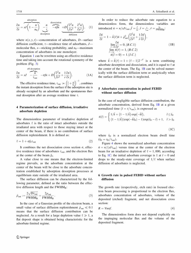
Figure 4 shows the normalized adsorbate concentration
�n ¼ n=ðsJsoutÞ versus time at the center of the electron
beam for an irradiative depletion of ~s ¼ 1; 000, according
to Eq. 1C: the initial adsorbate coverage is 1 at �t ¼ 0 and
drops to the steady-state coverage of 1=~s when surface
diffusion of adsorbates is neglected.
6 Growth rate in pulsed FEBID without surface
diffusion
The growth rate (respectively, etch rate) in focused elec-
tron beam processing is proportional to the electron flux,
adsorbates concentration of adsorbates, volume of the
deposited (etched) fragment, and net dissociation cross
section:
R ¼ Vnrf : ð4Þ
The dimensionless form does not depend explicitly on
the impinging molecular flux and the volume of the
deposited fragment.
1718 A. Szkudlarek et al.
123
�R ¼ R
sJV¼ ~s� 1ð Þ�f �n ¼ ~s� 1ð Þ2��r2
�n ¼ ~k � 1�
�n: ð4AÞ
Neglecting surface diffusion, the average growth (etch) rate
for pulsed exposure with an electron beam dwell time tD
(�tD ¼ tD=sout) is expressed as:
�R �tDð Þh it¼1
�tD
Z �tD
0
�Rð�tÞd�t �!~qout � 0:1
~k � 1
~k1þ ð~k � 1Þ 1� expð�~k�tDÞ
~k�tD
� � ð5Þ
Fig. 4 Evolution of normalized
surface coverage of adsorbates
at the electron beam center for a
given irradiative depletion
~s ¼ 1; 000. When the surface
diffusion contribution is
neglected, the normalized
surface coverage
(�n ¼ n=ðsJsoutÞÞ at the center of
the beam converges to the value
of 1=~s. The time evolution is
presented on the normalized
timescale (�t ¼ t=soutÞ:
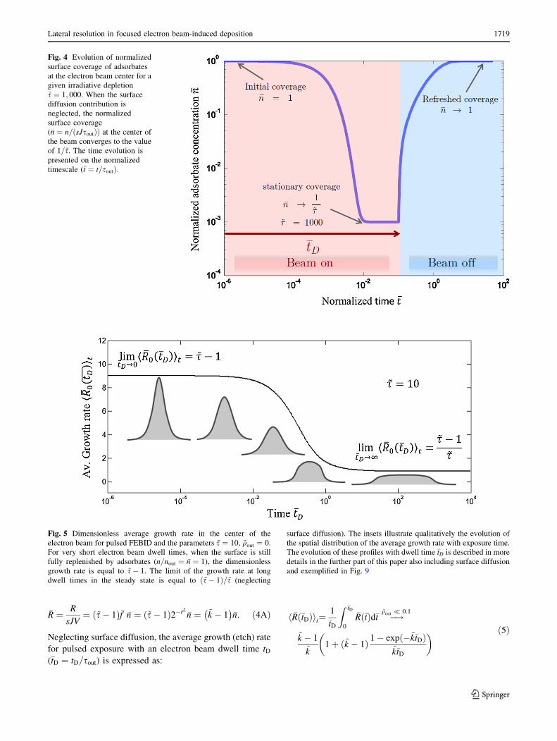
Fig. 5 Dimensionless average growth rate in the center of the
electron beam for pulsed FEBID and the parameters ~s ¼ 10, ~qout ¼ 0.
For very short electron beam dwell times, when the surface is still
fully replenished by adsorbates (n=nout ¼ �n ¼ 1), the dimensionless
growth rate is equal to ~s� 1. The limit of the growth rate at long
dwell times in the steady state is equal to ð~s� 1Þ=~s (neglecting
surface diffusion). The insets illustrate qualitatively the evolution of
the spatial distribution of the average growth rate with exposure time.
The evolution of these profiles with dwell time �tD is described in more
details in the further part of this paper also including surface diffusion
and exemplified in Fig. 9
Lateral resolution in focused electron beam-induced deposition 1719
123
The average growth rate in the center of the beam is
obtained by substitution of ~k ¼ ~k 0ð Þ ¼ ~s in Eq. 5:
�R0 �tDð Þh it¼~s� 1
~s1þ ð~s� 1Þ 1� expð�~s�tDÞ
~s�tD
� �; ð5AÞ
The limits of the deposition (etch) rate for very short and
long dwell times of the electron beam in the center of the
beam can be expressed in terms of the irradiative depletion
parameter:
lim�tD!0
�R0 �tDð Þh it¼ ~s� 1; ð5BÞ
lim�tD!1
�R0 �tDð Þh it¼~s� 1
~s: ð5CÞ
This means that for very short single-spot expo-
sures, the growth rate in the center of the electron
beam is a factor ~s larger than for long exposure times�tD � 1, see Fig. 5. Furthermore, with regard to the
spatial distribution of the growth rate for a single-spot
exposure, an increase in the dwell time results in the
transformation from a Gaussian toward a flattop aver-
age growth rate profile and to the related deposit or
etch shape profile.
7 Lateral resolution parameter
The lateral resolution parameter describes the lateral size of
the obtained deposit FWHMD with respect to the size of the
electron beam FWHMB and is defined as:
~u :¼ FWHMD
FWHMB
: ð6Þ
In the electron-limited regime, the deposit shape corre-
sponds to the Gaussian profile of the beam; therefore, it
assumes its smallest value which is equal to 1. Generally,
the value of the resolution parameter depends on the FE-
BID regimes illustrated in Fig. 1, and it can be estimated
by the scaling laws discussed below.
8 Scaling laws
The scaling laws introduced here correlate the lateral
deposit (or etch pit) size with the input parameters of the
FEBID model. They can be used to recalculate the surface
kinetics parameters of FEBID precursor adsorbates [15–17]
or to re-adjust exposure parameters to obtain a desired
lateral resolution or shape from the process.
1. First scaling law: stationary exposure without surface
diffusion
For the stationary-state solution, where no diffusion is
present, the lateral resolution parameter is a sole function
of irradiative adsorbate depletion ~u ~sð Þ. This scaling law
was introduced in [15]. For a Gaussian electron beam
profile distribution, it can be expressed as:
~u ¼ log2 1þ ~sð Þð Þ0:5: ð7Þ
2. Second scaling law: stationary exposure with surface
diffusion
Including surface diffusion by ~qout (see Eq. 3) results in
a new second scaling law for the lateral resolution given by
~u ffi log2 2þ ~s� 1
1þ ~q2out
� �� �0:5
ð8Þ
Figure 6a shows the excellent agreement of Eq. 8 with the
values derived from the numerical solution of Eq. 1B, which
has been solved using pdepe MATLAB� solver1 for one-
dimensional initial-boundary differential system and using
logarithmic transformation of the spatial variable l ¼ ln �rð Þ,which allows accounting for the adsorbates that are diffusing
over long distance far from the irradiated area [21].
Once the surface diffusion of adsorbates becomes strong
enough, the resolution parameter is carried to the electron-
limited regime with the best lateral resolution. A previ-
ously formulated scaling law in [17] is a special version of
Eq. 8, derived by substituting the surface diffusion
replenishment ~qout by an analogous parameter, defined at
the center of the beam ~qin ¼ ~qout=ffiffiffi~sp
. The version pre-
sented in [17] gives the lower limit of the surface diffusion
coefficient for a given observed lateral resolution of the
deposit (etch pit) and works well for large values of ~s [ 20.
The advantage of Eq. 8 is that it can be applied to small
values of the depletion parameter and allows to quickly
predict how changing the beam setup will influence the
lateral resolution, according to Eqs. 2 and 3.
3. Third scaling law: pulsed FEBID without surface
diffusion
Neglecting the surface diffusion term, a new third
scaling law can be formulated, describing the lateral res-
olution obtained in the FEBID (or etch) process as a
function of irradiative adsorbate depletion ~s and the nor-
malized electron beam dwell time �tD (see Eq. 1C):
~u ffi log2 2þ ~s� 1
1þ �t�1D
� �� �0:5
ð9Þ
For the short dwell times, the process is carried out in
the electron-limited regime and the resolution parameter is
equal to 1, see Fig. 6b. For long dwell times, it corresponds
to the values derived from the steady-state solution without
1 http://www.mathworks.com/help/matlab/ref/pdepe.html.
1720 A. Szkudlarek et al.
123
surface diffusion which are given by the first scaling law
(Eq. 7).
4. Fourth scaling law: pulsed FEBID with surface
diffusion
Including the surface diffusion term and taking into
account the duration of an electron pulse, a general fourth
scaling law can be formulated, describing the lateral res-
olution obtained in the FEBID (or etch) process as a
function of irradiative adsorbate depletion, normalized
electron beam dwell time, and surface diffusion
replenishment:
~u ffi log2 2þ ~s� 1
1þ �t�1D þ ~q2
out
� �� �0:5
ð10Þ
Figures 6c,d show the comparison of Eq. 10 with the
values derived from the numerical solution of Eq. 1B,
which has been obtained the analogous way as described in
point 2 of the current section. In this case, however, the
non-stationary state has been resolved in time.
For the electron-limited (reaction-limited) regime, the
resolution parameter is equal to 1. According to Eq. 10, it
can be reached by all the three parameters individually:
when the irradiative depletion ~s is close to 1, when the
Fig. 6 Illustration of the second, third, and fourth scaling laws for
lateral resolution ~u describing the size of FEB deposits or etch pits
which can be obtained by single-spot exposures: a second scaling
law: stationary electron beam exposure with surface diffusion—the
values for small surface diffusion converge to the first scaling law
(Eq. 7); b third scaling law: pulsed electron beam exposure, no
surface diffusion—the values corresponding to the long dwell times
are equal to those given by the first scaling law (Eq. 7); c, d fourth
scaling law: pulsed electron beam exposure with surface diffusion—
the deviations from simulations seen at long dwell times correspond
to the deviations seen in Fig. 6a. In (b–d), it can be seen that low
depletions can accept larger electron beam dwell times before the
regime transition from electron-limited to adsorbate-limited or
diffusion-enhanced occurs
Lateral resolution in focused electron beam-induced deposition 1721
123
surface diffusion replenishment ~qout is large enough to
overcome irradiative depletion, or with a very short elec-
tron beam exposure dwell time �tD per single spot. In gen-
eral, the process is carried out in the electron-limited
regime when the following statement is true
~s� 1
1þ �t�1D þ ~q2
out
� 1 ð11Þ
because then the square root term in Eq. 10 becomes 1. For
long electron beam exposure dwell times, the fourth scaling
law (Eq. 10) converges to the second scaling law (Eq. 8)
describing the steady-state solution with surface diffusion.
For negligible surface diffusion replenishment, the fourth
scaling law reduces to the third scaling law (Eq. 9)
describing pulsed FEBID without surface diffusion. For
long electron beam dwell times and negligible surface
diffusion, it converges to the analytical formula of the first
scaling law (Eq. 7) for stationary exposure conditions
without surface diffusion.
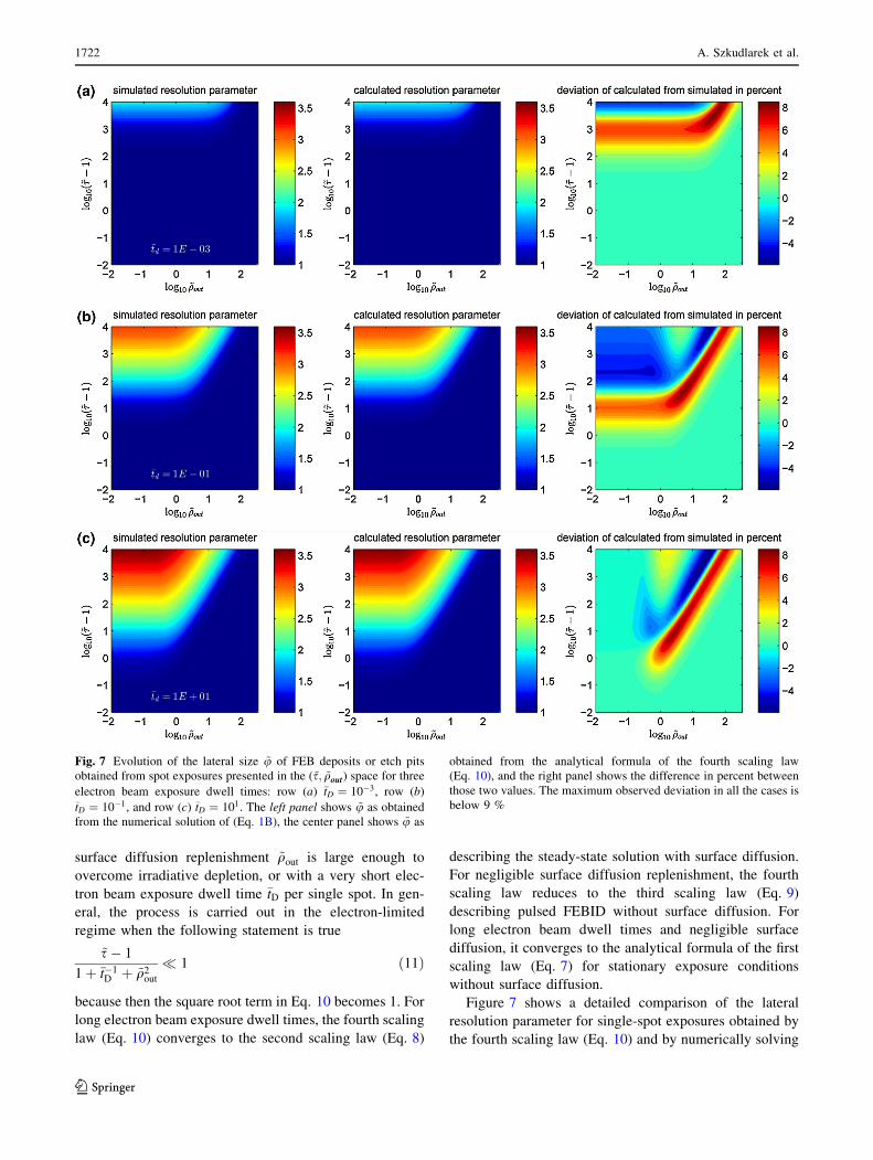
Figure 7 shows a detailed comparison of the lateral
resolution parameter for single-spot exposures obtained by
the fourth scaling law (Eq. 10) and by numerically solving
Fig. 7 Evolution of the lateral size ~u of FEB deposits or etch pits
obtained from spot exposures presented in the (~s; ~qout) space for three
electron beam exposure dwell times: row (a) �tD ¼ 10�3, row (b)�tD ¼ 10�1, and row (c) �tD ¼ 101. The left panel shows ~u as obtained
from the numerical solution of (Eq. 1B), the center panel shows ~u as
obtained from the analytical formula of the fourth scaling law
(Eq. 10), and the right panel shows the difference in percent between
those two values. The maximum observed deviation in all the cases is
below 9 %
1722 A. Szkudlarek et al.
123
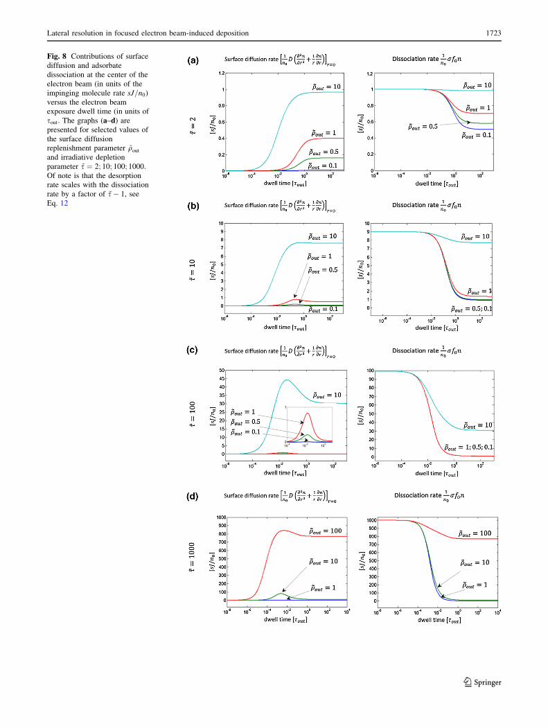
Fig. 8 Contributions of surface
diffusion and adsorbate
dissociation at the center of the
electron beam (in units of the
impinging molecule rate sJ=n0)
versus the electron beam
exposure dwell time (in units of
sout. The graphs (a–d) are
presented for selected values of
the surface diffusion
replenishment parameter ~qout
and irradiative depletion
parameter ~s ¼ 2; 10; 100; 1000.
Of note is that the desorption
rate scales with the dissociation
rate by a factor of ~s� 1, see
Eq. 12
Lateral resolution in focused electron beam-induced deposition 1723
123
the adsorption rate equations (Eqs. 1B and 5) for three
fixed electron beam exposure dwell times in the ð~s; ~qoutÞspace. The supplementary information contains an anima-
tion which covers the full evolution of the lateral size of
deposits or etch pits in the range of dwell times
�tD 2 10�6; 103�
.
9 Contributions of surface diffusion and adsorbate
dissociation in pulsed exposure
In order to study the contributions of surface diffusion and
dissociation at a certain duration of the exposure, we calcu-
lated the terms of Eq. 1A at the center of the beam (r ¼ 0) for
selected values of the ~s; ~qout input parameter space. The
results presented in Fig. 8 (a–d) are given in units of the
impingement rate of molecules (sJ=n0Þ (in units of s�1).
The left column panels of Fig. 8 show the diffusion rates
1n0
D o2nox2 þ o2n
oy2
� �(in units of s-1) at the center of the beam
for a given value of ~s. Only for the small values of
depletion (~s\10), the surface diffusion rate increases
monotonously, whereas for the higher depletions a peak
appears. The surface diffusion rate at small electron beam
dwell times is monotonously rising since the divergence of
the adsorbate concentration gradient increases between the
inside and outside of the irradiated area due the increasing
dwell time, see Fig. 4. The surface diffusion rate plateaus
when the steady-state depletion is reached and, for large
depletions decays again. This situation is equivalent to the
indent shape formation shown in Fig. 9b; due to the
efficient electron-triggered dissociation of surface diffusion
adsorbates at the rim of the irradiated area, the center of the
deposit is not replenished anymore at longer dwell times.
From Fig. 8, it becomes obvious that starting from at a
certain dwell time, the diffusive replenishment can become
orders of magnitude larger than the replenishment from the
gas phase. This was an explanation why FEBID structures
fabricated with an intermediate dwell time show a smaller
roughness than those with the shortest dwell time values
[26]. It can also be an explanation for morphology effects
in FEBID structures obtained with different scanning
strategies [27] and for the effects of chemical composition
changes in two adsorbate systems [28].
In the right column panels of Fig. 8, the adsorbate dis-
sociation rate rf0n=n0 (in units of s�1) is shown, which is
proportional to the growth rate, see Eq. 4. For the very
short dwell times, the growth rate at the center of the beam
is constant and equal to ð~s� 1ÞsJV , see also Eq. 5B. It
starts to decrease at a given value of the dwell time, which
is correlated to the depletion parameter. The limit for
the long dwell times depends on the diffusion contribution.
For the small values of surface diffusion parameter
ð~qout � 0:1Þ, the stationary growth rate is equal to
ð~s� 1ÞsJV=~s, see also Eq. 5C.
The effective desorption rate 1n0
nsout
is not explicitly pre-
sented in Fig. 8 but scales according to Eq. 2 as:
1
n0
n
sout
¼ 1
n0
rf0n
ð~s� 1Þ ; ð12Þ
i.e., it is equal to the dissociation rate shown in Fig. 8
divided by the factor ~s� 1.
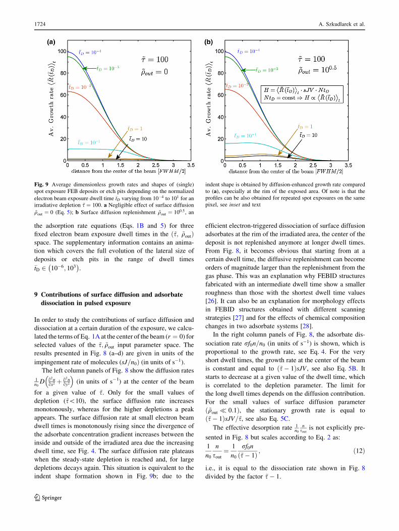
Fig. 9 Average dimensionless growth rates and shapes of (single)
spot exposure FEB deposits or etch pits depending on the normalized
electron beam exposure dwell time �tD varying from 10�4 to 101 for an
irradiative depletion ~s ¼ 100. a Negligible effect of surface diffusion
~qout ¼ 0 (Eq. 5); b Surface diffusion replenishment ~qout ¼ 100:5, an
indent shape is obtained by diffusion-enhanced growth rate compared
to (a), especially at the rim of the exposed area. Of note is that the
profiles can be also obtained for repeated spot exposures on the same
pixel, see inset and text
1724 A. Szkudlarek et al.
123
10 Influence of the electron beam dwell time �tD
and surface diffusion replenishment ~qout
on the shape of the deposit or etch pit
In the case of negligible surface diffusion replenishment
~qout � 0:1, the analytical formula for the average growth
rate �Rð�tDÞh it in Eq. 5 can be used to calculate the shape.
The case of surface diffusion replenishment greater than
0.1 necessitates a numerical solution of Eq. 1B for the
coverage �nð�r; �tÞ together with a numerical integration of
Eq. 5. Figure 9 illustrates the solution for the cases of
~qout ¼ 0 and ~qout ¼ 100:5 and for dimensionless dwell
times �tD varying from 10-4 to 101.
The curves in Fig. 9 are generally strictly correct for a
single-spot exposure having the boundary and initial con-
ditions stated in Eqs. 1B. The shape of the deposit (thick-
ness) or etch pit (depth) is then simply obtained by
multiplying with the electron beam exposure dwell time.
Choosing a refresh time long enough for a complete sur-
face replenishment of adsorbates, the shape profiles H for
repeated spot exposures (on the same pixel) can be
obtained by multiplying by the dwell time tD and the
number of pulse repetitions N:
H r; tDð Þ ¼ R tD; rð Þh itNtD ¼ �R �tD; �rð Þh it�sJV � NtD ð13Þ
Keeping the dose constant for all exposures in Fig. 9,
i.e., keeping the product of number of repetitions and pulse
time N � tD constant, the curves in Fig. 9 would correspond
to the exact shape profiles obtained at a given dose. Fig-
ure 9 is also an illustration of how the growth rate evolves
during a spot exposure: it is Gaussian at very low electron
beam dwell times and undergoes all profiles from rounded,
flattop (negligible surface diffusion), to indent. These
profiles relate to different regimes as shown in Fig. 1.
According to the dwell time chosen in an exposure
experiment, the FEB growth or etching will thus proceed in
various regimes. The consequence even for single-spot
deposits is that the bottom layer could be deposited in the
electron-limited regime while the top layer parts would be
deposited in the adsorbate-limited/diffusion-enhanced
regime, i.e., the resulting deposit material would be inho-
mogeneous with thickness, which is especially important
for electrical contacts of FEBID material with electrodes.
11 Conclusions
In this work, we presented a new approach to the con-
tinuum model for pulsed FEBID, with a set of parameters
{~s; ~qout}, describing independently the surface diffusion
and the dissociation contributions, which couple the sur-
face kinetics parameters of adsorbates with the electron
beam settings. The growth rate for pulsed FEBID is
expressed as function of the adsorbate depletion parameter
with the respective limits for short and long dwell times.
The application of dimensionless parameters allows us to
predict how changes in the electron beam setup will
influence the process and how it will determine the deposit
shape. Three new analytical scaling laws governing the
lateral size of deposits or etch pits in gas-assisted focused
electron beam-induced processing were formulated as
function of the adsorbate surface diffusion term, the
electron beam dwell time for a single-spot exposure, and
the irradiative adsorbate depletion. The analytical scaling
laws were mapped against the exact simulation results and
show very good agreement. The maximum mapped error
in the variable space was about 8 %. The evolution of the
contributions of surface diffusion and electron-induced
adsorbate dissociation as a function of electron beam
dwell (exposure) time was calculated in detail from the
numerical solution, showing a peak of the surface diffu-
sive replenishment at the center of the irradiated area at a
certain exposure time being significantly higher than the
replenishment by the impinging molecular precursor flux
from the gas phase. The decay of surface diffusion
replenishment at the center for short and long exposure
dwell times is due to the low divergence of the adsorbate
profile and the dissociation of adsorbates at the rim of the
irradiated area, respectively, and results in specific deposit
shapes and eventually material along the period of
exposure.
Acknowledgments The authors would like to acknowledge the
contribution of the COST Action MP0901.
Open Access This article is distributed under the terms of the
Creative Commons Attribution License which permits any use, dis-
tribution, and reproduction in any medium, provided the original
author(s) and the source are credited.
References
1. I. Utke, A. Golzhauser, Angew. Chem. Int. Ed. 49 (2010). doi:10.
1002/anie.201002677
2. J.M. De Teresa, A. Fernandez-Pacheco, R. Codoba, J. Sese, M.R.
Ibarra, I. Guillamon, H. Suderow, S. Vieira, MRS proc. CC04-09,
1880 (2009)
3. A. Fernandez-Pacheco, J.M. De Teresa, A. Szkudlarek, R. Cor-
doba, M.R. Ibarra, D. Petit, L. O’Brien, H.T. Zeng, E.R. Lewis,
D.E. Read, R.P. Cowburn, Nanotechnology (2009). doi:10.1088/
0957-4484/20/47/475704
4. M. Gavagnin, H.D. Wanzenboeck, D. Belic, E. Bertagnolli, ACS
Nanotechnol. (2012). doi:10.1021/nn305079a
5. T. Brintlinger, M.S. Fuhrer, J. Melngailis, I. Utke, T. Bret, A.
Perentes, P. Hoffmann, M. Abourida, P. Doppelt, J. Vac. Sci.
Technol. B 23, 3174 (2005). doi:10.1116/1.2130355
6. S. Kim, D. Kulkarni, K. Rykaczewski, M. Henry, V.V. Tsukruk,
A. Fedorov, IEEE Trans. Nanotechnol. 11(6), 1223–1230 (2012).
doi:10.1109/TNANO.2012.2220377
Lateral resolution in focused electron beam-induced deposition 1725
123
7. ChH Schwalb, Ch. Grimm, M. Baranowski, R. Sachser, F. Por-
rati, H. Reith, P. Das, J. Muller, F. Volklein, A. Kaya, M. Huth,
Sensors (2010). doi:10.3390/s101109847
8. M. Gabureac, L. Bernau, I. Utke, G. Boero, Nanotechnology
(2010). doi:10.1088/0957-4484/21/11/115503
9. F. Kolb, K. Schmoltner, M. Huth, A. Hohenau, J. Krenn, A. Klug,
E.J. List, H. Plank, Nanotechnology (2013). doi:10.1088/0957-
4484/24/30/305501
10. K. Hoflich, R.B. Yang, A. Berger, G. Leuchs, S. Christiansen,
Adv. Mater. 23. (2011). doi:10.1002/adma.201004114
11. I. Utke, M.G. Jenke, Ch. Roling, P.H. Thiesen, V. Iakovlev, A.
Sirbu, A. Mereuta, A. Calimanc, E. Kaponc, Nanoscale (2011).
doi:10.1039/C1NR10047E
12. A. Perentes, P. Hoffmann, J. Vac. Sci. Technol. B 25, 2233
(2007). doi:10.1116/1.2798746
13. H.D. Wanzenboeck, M. Fischer, R. Svagera, J. Wernisch, E.
Bertagnolli, J. Vac. Sci. Technol. B 24, 2755 (2006). doi:10.1116/
1.2393245
14. I. Utke, P. Hoffmann, J. Melngailis, J. Vac. Sci. Technol. B 26, 4
(2008). doi:10.1116/1.2955728
15. I. Utke, V. Friedli, M. Purrucker, J. Michler, J. Vac. Sci. Technol.
B 25, 6 (2007). doi:10.1116/1.2789441
16. A. Szkudlarek, M. Gabureac, I. Utke, J. Nanosci. Nanotechnol.
11, 9 (2011). doi:10.1166/jnn.2011.5066
17. J.D. Fowlkes, P.D. Rack, ACS Nano (2010). doi:10.1021/
nn901363a
18. M.G. Lassiter, P.D. Rack, Nanotechnology (2008). doi:10.1088/
0957-4484/19/45/455306
19. S. Randolph, M. Toth, J. Cullen, C. Chandler, Ch. Lobo, Appl.
Phys. Lett. 99, 213103 (2011). doi:10.1063/1.3662928
20. M. Toth, Ch.J. Lobo, G. Hartigan, W.R. Knowles, J. Appl. Phys.
101, 054309 (2007). doi:10.1063/1.3662928
21. Ch.J. Lobo, M. Toth, R. Wagner, B.L. Thiel, M. Lysaght,
Nanotechnology (2008). doi:10.1088/0957-4484/19/02/025303
22. L. Bernau, M. Gabureac, R. Erni, I. Utke, Angew. Chem. Int. Ed.
49. (2010). doi:10.1002/anie.201004220
23. M. Huth, F. Porrati, Ch. Schwalb, M. Winhold, R. Sachser, M.
Dukic, J. Adams, G. Fantner, Beilstein J. Nanotechnol. (2012).
doi:10.3762/bjnano.3.70
24. J. Bishop, Ch.J. Lobo, A. Martin, M. Ford, M. Phillips, M. Toth,
Phys. Rev. Lett. 109, 146103 (2012). doi:10.1103/PhysRevLett.
109.146103
25. W.F. van Dorp, Th.W. Hansen, J.B. Wagner, J.T.M. De Hosson,
Beilstein J. Nanotechnol. (2013). doi:10.3762/bjnano.4.56
26. R. Winkler, J. Fowlkes, A. Szkudlarek, I. Utke, PhD Rack,
H. Plank, ACS Appl. Mater. Interfaces (2014). doi:10.1021/
am405591d
27. A. Szkudlarek, M. Gabureac, I. Utke, ECS Trans. 50. (2013).
doi:10.1149/05012.0495ecst
28. M. Gabureac, L. Bernau, I. Utke, J. Nanosci. Nanotechnol. 11, 9
(2011). doi:10.1166/jnn.2011.5067
1726 A. Szkudlarek et al.
123
Related Documents