Laser Prototyping of Microwave Circuits in LTCC Technology M. Farhan Shafique, Student Member, IEEE, Kashif Saeed, Member, IEEE, David Paul Steenson, Senior Member, IEEE, and Ian D. Robertson, Senior Member, IEEE Abstract—In this paper, a process for direct laser structuring of microwave circuits in low-temperature co-fired ceramic (LTCC) technology is reported. An efficient alternative to screen printing is proposed for prototyping circuits by laser patterning the con- ductors on the unfired tape. A line width and gap of 50 m are achieved with laser machining. A range of samples has been studied using a scanning electron microscope in order to optimize the process parameters. The surface roughness of laser-treated samples is measured with a surface profiler and compared with the untreated samples. A method of creating microvias and trenches in thick LTCC substrate is also demonstrated. For 254 m thick green tape, vias with a diameter and separation of 50 m are realized along with trenches having a width as small as 30 m. The method of optimizing the laser machining process is described in detail. A band-stop mushroom resonator and a microstrip ring resonator filter are fabricated and their results compared against simulations. Index Terms—Ceramics, laser machining, low-temperature co-fired ceramic (LTCC), microwave circuits, multichip modules, thick film circuits. I. INTRODUCTION W HILE silicon-based system-on-chip technology con- tinues to advance rapidly, in microwave, millimeter- wave and terahertz systems there remains a demand for packaging solutions that provide the ability to integrate semi- conductor devices from a wide range of technologies [1], [2]. Ceramic multichip module technology (MCM-C) is an excel- lent candidate for this packaging requirement. It can provide embedded passive components, hermeticity, and excellent thermal and mechanical stability. Thick-film technology is a well-established traditional technique for microelectronic packaging. The layers of dielectric and conductor are printed sequentially onto the alumina substrate. However, for sophis- ticated multilayer thick-film fabrication [3], any small defect may require a complete rebuild of the whole design and the need for repeated firing cycles can make the fabrication process very time consuming. Manuscript received April 15, 2009; revised July 27, 2009. First published November 13, 2009; current version published December 09, 2009. This work was supported in part by the Engineering and Physical Sciences Research Council under Grant EP/D068649/1 and in part by the COMSATS Institute of Information Technology, Islamabad, Pakistan. The authors are with the Institute of Microwaves and Photonics, School of Electronic and Electrical Engineering, The University of Leeds, Leeds LS2 9JT, U.K. (e-mail: [email protected]; [email protected]). The alternatives to thick-film technology are high tempera- ture co-fired ceramic (HTCC) and low-temperature co-fired ce- ramic (LTCC). The repeated firing drawback of thick-film tech- nology is overcome in these two technologies by cofiring the complete circuit after laminating all the layers together. LTCC has an advantage of low temperature sintering over HTCC. This low temperature sintering allows the use of high conductivity metals like gold, silver and copper. The parallel processing of layers in LTCC technology allows the replacement of a defec- tive layer at any stage before laminating. The tracks are usually screen (or stencil) printed on individual layers and a width and gap of 100 m are achievable with fine mesh screens. For a so- phisticated multilayer LTCC design, a large number of screens are required to pattern the conductors and filling the vias on different layers, making prototyping of a new design relatively costly and time consuming. There are various alternatives to directly screen-printing the conductor patterns. Photoimageable inks can be printed and pat- terned photolithographically [4], although this requires high res- olution masks and a controlled light environment [5]. These photoimageable inks can yield tracks as small as 10 m [5]. Other techniques like inkjet and micropen deposition can be used for a range of electronic and organic materials with pre- cision and high resolution [6]. A technique known as thermal spray is also useful, in which inks are sprayed at high velocity and solidify when they land on the substrate [6]. High capital investment is mandatory for the techniques such as focused ion beams and nanolithography, although they do give outstanding resolution. Laser-induced forward transfer (LIFT) is another well developed technique where a laser beam transfers mate- rial from an optically transparent ribbon onto the substrate. An organic vehicle is mixed with the depositing material to im- prove the process quality and it is known as matrix-assisted pulsed laser evaporation direct writing (MAPLE-DW) [6], [7]. These various processes have different tradeoffs with respect to process quality, turnaround time of prototyping and capital investment required. A very attractive solution for microwave circuit prototyping is achieved with direct laser machining of unfired ceramics [8]. The process is very fast and does not re- quire chemicals or a controlled light environment. Moreover, this technique provides a significant reduction of fabrication time (to a few hours) and also allows the freedom to change a design without requiring any new screens or masks. In a recent study, the laser processing of different materials was studied; fired alumina coated with platinum and gold was treated with a frequency tripled Nd:YAG laser and laser struc- turing of laminated green tapes was also commented on briefly

Welcome message from author
This document is posted to help you gain knowledge. Please leave a comment to let me know what you think about it! Share it to your friends and learn new things together.
Transcript
3254 IEEE TRANSACTIONS ON MICROWAVE THEORY AND TECHNIQUES, VOL. 57, NO. 12, DECEMBER 2009
Laser Prototyping of Microwave Circuitsin LTCC Technology
M. Farhan Shafique, Student Member, IEEE, Kashif Saeed, Member, IEEE,David Paul Steenson, Senior Member, IEEE, and Ian D. Robertson, Senior Member, IEEE
Abstract—In this paper, a process for direct laser structuring ofmicrowave circuits in low-temperature co-fired ceramic (LTCC)technology is reported. An efficient alternative to screen printingis proposed for prototyping circuits by laser patterning the con-ductors on the unfired tape. A line width and gap of 50 m areachieved with laser machining. A range of samples has beenstudied using a scanning electron microscope in order to optimizethe process parameters. The surface roughness of laser-treatedsamples is measured with a surface profiler and compared with theuntreated samples. A method of creating microvias and trenchesin thick LTCC substrate is also demonstrated. For 254 m thickgreen tape, vias with a diameter and separation of 50 m arerealized along with trenches having a width as small as 30 m.The method of optimizing the laser machining process is describedin detail. A band-stop mushroom resonator and a microstrip ringresonator filter are fabricated and their results compared againstsimulations.
Index Terms—Ceramics, laser machining, low-temperatureco-fired ceramic (LTCC), microwave circuits, multichip modules,thick film circuits.
I. INTRODUCTION
W HILE silicon-based system-on-chip technology con-tinues to advance rapidly, in microwave, millimeter-
wave and terahertz systems there remains a demand forpackaging solutions that provide the ability to integrate semi-conductor devices from a wide range of technologies [1], [2].Ceramic multichip module technology (MCM-C) is an excel-lent candidate for this packaging requirement. It can provideembedded passive components, hermeticity, and excellentthermal and mechanical stability. Thick-film technology isa well-established traditional technique for microelectronicpackaging. The layers of dielectric and conductor are printedsequentially onto the alumina substrate. However, for sophis-ticated multilayer thick-film fabrication [3], any small defectmay require a complete rebuild of the whole design and theneed for repeated firing cycles can make the fabrication processvery time consuming.
Manuscript received April 15, 2009; revised July 27, 2009. First publishedNovember 13, 2009; current version published December 09, 2009. This workwas supported in part by the Engineering and Physical Sciences ResearchCouncil under Grant EP/D068649/1 and in part by the COMSATS Institute ofInformation Technology, Islamabad, Pakistan.
The authors are with the Institute of Microwaves and Photonics, School ofElectronic and Electrical Engineering, The University of Leeds, Leeds LS2 9JT,U.K. (e-mail: [email protected]; [email protected]).
Color versions of one or more of the figures in this paper are available onlineat http://ieeexplore.ieee.org.
Digital Object Identifier 10.1109/TMTT.2009.2033846
The alternatives to thick-film technology are high tempera-ture co-fired ceramic (HTCC) and low-temperature co-fired ce-ramic (LTCC). The repeated firing drawback of thick-film tech-nology is overcome in these two technologies by cofiring thecomplete circuit after laminating all the layers together. LTCChas an advantage of low temperature sintering over HTCC. Thislow temperature sintering allows the use of high conductivitymetals like gold, silver and copper. The parallel processing oflayers in LTCC technology allows the replacement of a defec-tive layer at any stage before laminating. The tracks are usuallyscreen (or stencil) printed on individual layers and a width andgap of 100 m are achievable with fine mesh screens. For a so-phisticated multilayer LTCC design, a large number of screensare required to pattern the conductors and filling the vias ondifferent layers, making prototyping of a new design relativelycostly and time consuming.
There are various alternatives to directly screen-printing theconductor patterns. Photoimageable inks can be printed and pat-terned photolithographically [4], although this requires high res-olution masks and a controlled light environment [5]. Thesephotoimageable inks can yield tracks as small as 10 m [5].Other techniques like inkjet and micropen deposition can beused for a range of electronic and organic materials with pre-cision and high resolution [6]. A technique known as thermalspray is also useful, in which inks are sprayed at high velocityand solidify when they land on the substrate [6]. High capitalinvestment is mandatory for the techniques such as focused ionbeams and nanolithography, although they do give outstandingresolution. Laser-induced forward transfer (LIFT) is anotherwell developed technique where a laser beam transfers mate-rial from an optically transparent ribbon onto the substrate. Anorganic vehicle is mixed with the depositing material to im-prove the process quality and it is known as matrix-assistedpulsed laser evaporation direct writing (MAPLE-DW) [6], [7].These various processes have different tradeoffs with respectto process quality, turnaround time of prototyping and capitalinvestment required. A very attractive solution for microwavecircuit prototyping is achieved with direct laser machining ofunfired ceramics [8]. The process is very fast and does not re-quire chemicals or a controlled light environment. Moreover,this technique provides a significant reduction of fabricationtime (to a few hours) and also allows the freedom to changea design without requiring any new screens or masks.
In a recent study, the laser processing of different materialswas studied; fired alumina coated with platinum and gold wastreated with a frequency tripled Nd:YAG laser and laser struc-turing of laminated green tapes was also commented on briefly
0018-9480/$26.00 © 2009 IEEE
SHAFIQUE et al.: LASER PROTOTYPING OF MICROWAVE CIRCUITS IN LTCC TECHNOLOGY 3255
[9]. In a study of microheaters [10], a laser was used to patternconductors on green tape with a gap as small as 80 m and widthof 50 m.
The realization of microvias with fine spacing is important formillimeter-wave applications. For example, substrate integratedwaveguides [11]–[13] have a wide range of applications andrequire precisely-fabricated vias or trenches to form sidewalls[14]. Trenches are also important for microfluidic applicationsof LTCC [15] in which a few microliters of liquid sample can bechanneled for analysis. An integrated cooling system in LTCChas also been reported using channels to supply air or liquid toreduce the temperature of a module [16].
Mechanical tools for drilling or punching vias have the dis-advantage that direct contact with the substrate will lead to toolwear and damage. Laser machining, on the other hand, doesnot involve any direct contact with the substrate. Various lasersystems are commercially available and different studies showthe advantages of each laser types [16], [17]. Vias as smallas 75 m were drilled in 254 m thick substrate with 15 mbeam Nd:YVO4 laser [18]. The flexibility of laser processingalso opens up a range of new applications for LTCC technology[19], [20].
In this study, we have concentrated on the laser machiningof conductors on unfired green tapes [8]. The effects of varyinglaser parameters on a single green tape with printed conductorhave been examined in detail. A technique for optimizing thedirect laser machining is devised. The laser treated samples arecompared with untreated samples for their surface roughness.A process of making trenches and microvias as small as 50 min thick green tapes is discussed. The process is then utilizedto fabricate microwave resonators. We have used the commer-cially available ProtoLaser 200 Nd:Yag laser-based system fromLPKF laser and electronics. It provides good control of the dif-ferent laser parameters which are critical for fine-line proto-typing. The LTCC material shows low absorption when exposedto the 1024 nm Nd:Yag laser, ablation of material occurs and thegasses are extracted with a vacuum pump [21], [22]. This abla-tion helps in cutting clean vias. In order to observe the samplesunder a scanning electron microscope (SEM), they were pre-pared by evaporating gold onto fired green tapes. To comparethe surface roughness of etched and unetched samples, the alphaI/Q surface profiler was used.
II. PROCESS OVERVIEW
DuPont 943PX green tape dielectric with 254 m thicknesswas used in this study. Silver-based conducting paste HF612from DuPont was used for printing. The green tape was pre-conditioned in an oven at 120 C for 30 min to undergo ini-tial shrinkage. The tape has plastic backing for its surface pro-tection. The tape was loaded in the laser machine along withthe plastic backing to drill vias and fiducials. The fiducials arenecessary for later stages of laser machining and alignment. Alarger number of fiducials helps in achieving better alignment ofthe substrate. The vias in the green tape were metalized using ascreen printer. As a further aid to rapid prototyping, the plasticbacking can be used as a stencil for the printing of via-fill con-ductor paste. A porous suction plate forces the paste into the
TABLE ILASER PARAMETERS
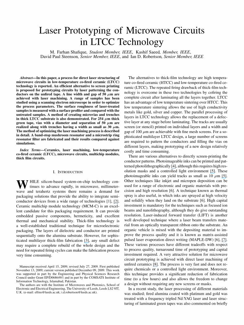
Fig. 1. Hatch lines and contour line.
vias when printed with a screen printer. The viscosity and par-ticle size of paste are important for the optimum filling of vias.An appropriate thinner can be added to the paste to adjust its vis-cosity. After filling the vias the plastic backing was removed anda square patch of 100 mm 100 mm was printed using a stan-dard 280 screen mesh with the emulsion thickness of 10 m.This resulted in a dried patch of 20 m thickness. It is recom-mended to print the patch without drying the vias as this willguarantee a proper contact. The green tape was then dried at80 C for 10 min in an oven.
This green tape was then loaded into the laser machine withthe help of fiducials to ensure the proper alignment with the data.The controlled laser etching on the tape removed the unwantedsilver, leaving the tracks and gaps. The energy from photonsconverts into heat on striking the silver. This heat evaporates thesilver and the fumes can be extracted with a vacuum pump. Thesubstrate surface suffers some damage and a layer of a few mi-crometers thickness is ablated along with the silver. The processwas repeated for other layers and these layers were then alignedwith the help of fiducials and pressed in an isostatic laminatorat 30 MPa and 70 C for 10 min followed by cofiring in a pro-grammable box furnace.
III. LASER ETCHING
The laser used in this study has square beam shape of25 m 25 m that is focused with a combination of lenses.The characteristics of the laser equipment are shown in Table I.The laser software uses a Gerber file. It fills the empty back-ground area with horizontal lines. These lines are referred ashatch lines. A special line which encloses the design edges iscalled the contour line as shown in Fig. 1. The pitch of thehatch lines, known as the hatch grid, and the contour line areadjustable. These lines represent the tracks which the laserbeam follows on the substrate. The power, writing speed andpulse repetition rate of the laser are controllable. To analyze
3256 IEEE TRANSACTIONS ON MICROWAVE THEORY AND TECHNIQUES, VOL. 57, NO. 12, DECEMBER 2009
TABLE IIWRITING SPEED OBSERVATIONS
these parameters, square patches of 15 mm 15 mm wereetched on green tape. Only one parameter was varied at a time,keeping others constant around their mean values. However, thedependant variables were adjusted to keep the ratio constant.This scenario is explained in more detail later. The results ob-tained were averaged from ten samples to reduce the ambiguity.
A. Writing Speed and Pulse Rate
The writing speed and pulse rates are two important param-eters that are related to each other. A high pulse repetition ratewith high writing speed helps to complete the job quickly. Thesetwo parameters were adjusted to keep the overlap between thetwo successive pulses constant. This overlap becomes more sig-nificant when a Gaussian or top-hat beam profile is used. Theoverlap of half of a beam diameter can be used as a rule of thumbas this will cover almost every beam profile. The hatching gridwas set to be 16 m. With the increase of writing speed the pulserate was increased to keep the overlap constant.
It was observed that even changing these parameters witha constant ratio made a significant difference; a high writingspeed produced less absorption in the silver as compared tolow writing speed. The dominant variable is the writing speed;a slow writing speed resulted in more damage to the substratesurface. The speed was varied from 100 to 1000 mm/s with theoverlap ratio kept at 12.5 m. The laser penetrated the substrateas deep as 30 m into the substrate for writing speeds below 150mm/s. As the speed was increased above 200 mm/s the substratedamage reduced to less than 5 m, although the silver residueincreased. These observations are summarized in Table II [8].
B. Laser Power
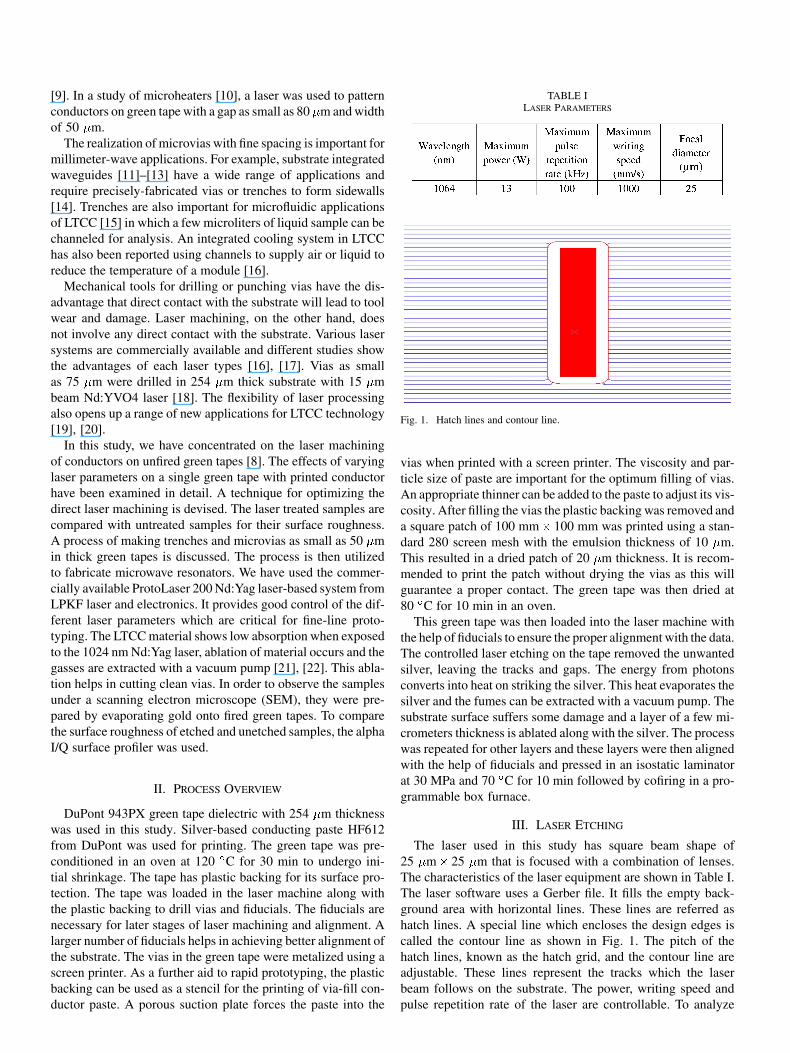
The laser power affects the substrate directly withoutdepending on any other parameter and is the most critical pa-rameter. The green tape being soft in nature is easily damagedwith high laser power. When the maximum power of 13 Wwas used, the laser burnt the substrate badly and created a holein the substrate. The same results were observed even withincreasing the writing speed to 1000 mm/s. The laser powerwas then varied from 3.5 to 10.5 W while keeping the writingspeed constant at 500 mm/s and the pulse rate at 40 kHz. Itwas observed that the substrate damage was as deep as 30 mwhen the power was set above 7.8 W. At powers less than 5W, the silver was not removed at all. However, laser powerbetween 5.2 and 7.5 W created the peel off effect. This powerrange is high enough to peel off the silver, leaving the substratewith little silver. This effect is shown in Fig. 2. The peel-offeffect left a silver residue when used over larger areas. Theobservations are listed in Table III [8].
Fig. 2. Peel-off effect.
TABLE IIILASER POWER OBSERVATIONS
C. Hatching Grid
The hatching grid is the pitch of the hatch lines as shown inFig. 1. The writing speed and pulse repetition rate define thesubstrate smoothness in one dimension and the hatching griddefines the smoothness in the other dimension. It is a good ideato keep the hatching grid and the ratio of writing speed to pulserepetition rate the same to achieve uniform smoothness over alarger area. This grid is defined with reference to beam shape;for Gaussian and top-hat laser profiles, this grid can be set tohalf of the beam diameter. The etching time can be reduced byincreasing the gap as long as it is not leaving any un-etched areabetween two adjacent hatch tracks.
After analyzing the parameters individually, it was concludedthat these parameters cannot be optimized separately as theyare interdependent. So, an optimization procedure needed to bedevised to use this technique efficiently.
IV. OPTIMIZATION OF LASER PARAMETERS
The laser parameters were optimized while keeping in mindthe objective of high writing speed, low substrate damage, andsmooth conductor edges. The conductor was etched generallyfrom the substrate followed by etching the contour line to im-prove the edge resolution. However, in removing silver from thegreen tape, if the silver is etched before contouring, then cracksmay appear in narrow tracks so the contour is etched first toisolate the tracks from the remaining silver, thus preventing theoverheating of tracks during the etching of the substrate.
The contour lines are important in the process optimizationas they define the edge resolution. The hatch lines can have dif-ferent parameter settings to the contour lines. The first thing tocheck in optimization of these parameters is the laser absorp-tion by the silver. The maximum writing speed of 1000 mm/swas set to reduce the processing time with the pulse rate of 80kHz that gives a pulse overlap of 12.5 m; even with the squarebeam profile, a half beam diameter overlap is recommended toavoid ragged edges. A straight line was etched in the silver andthe gap width was studied.
SHAFIQUE et al.: LASER PROTOTYPING OF MICROWAVE CIRCUITS IN LTCC TECHNOLOGY 3257
Fig. 3. Substrate damage around the contour line: (A) silver track itself;(B) contour line; and (C) etched substrate region.
At a power of 6.7 W, the gap is 80 m wide, meaning thatthe 25 m beam was creating the gap of 80 m. This absorptionshould be reduced to achieve the smaller gaps. The power wasthen reduced to 5.8 W to restrict the absorption to 50 m. At thislaser power, the silver was not removed completely, so the linewas etched three times to ensure the complete removal of silver.After three equal power contour cycles, the substrate underneaththe contour line was not affected much more than the remainingarea. This is shown in Fig. 3. An average of 5 m extra damagewas observed under the contour lines.
To properly remove the silver from the substrate surface, thepeel-off effect was targeted. A power of 5.9 W was used to peeloff the silver with a writing speed of 500 mm/s and pulse rate of40 kHz. The remaining silver on the substrate was removed in asecond cycle by reducing the power to 5.2 W and increasing thewriting speed to 800 mm/s and the pulse repetition frequencyto 65 kHz, A third cycle at a power of 4.4 W may be added toimprove the smoothness of the etched substrate.
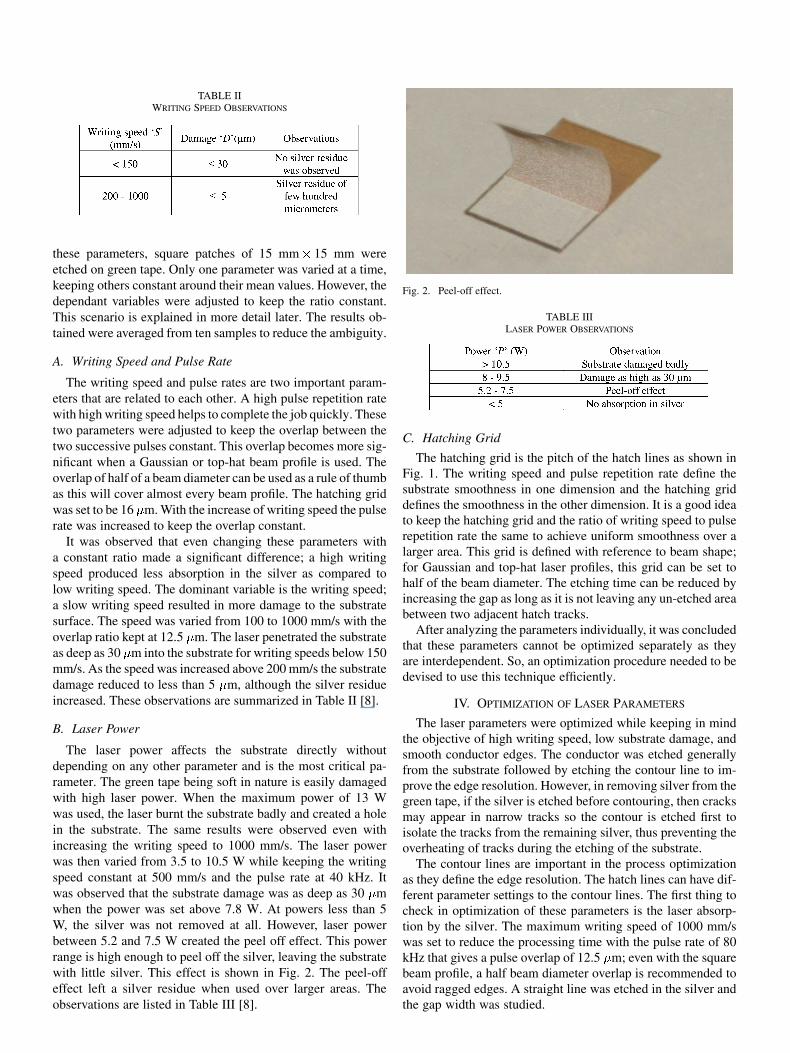
The most challenging part of this phase is minimizing the heattransfer to the conductor tracks. If the design has tracks of 50 mwidth then they can be damaged easily by slight overheating fromthe hatch lines. If we observe Fig. 1, the hatch lines end on thecontour line on one side of the track and starts again on the otherside. To avoid overheating the narrow tracks, the laser was turnedoff shortly before reaching the contour line, which left a few mi-crometers of unetched substrate. Similarly, on the other side thelaser was turned on at the hatch line with a short delay so thatthe laser was few micrometers away from the contour line. Thesilver on both sides that was not directly etched had, however,gained sufficient energy from the beginning or end of the hatchline to peel itself off the substrate, thus leaving no silver behind.This phenomenon is shown in Fig. 4, which is an SEM photo-graph of a fired sample with a 100 m conductor track; the ver-tical white lines drawn on the picture show the contour line andthe horizontal lines represent the hatch lines. The trench labeled“A” is the etched region from the contour line and region “C” isthe etched region from the hatch lines. A small hump is visiblebetween the two regions, labeled region“B”; it represents the por-tion that is not directly etched with the laser so the substrate is notdamaged but the silver is peeled off by absorbing sufficient heat.
Another technique to improve the edge resolution is to add anextra contour line. The two contour lines were etched first and
Fig. 4. SEM photograph of laser etched 100 �m track with single contour line.
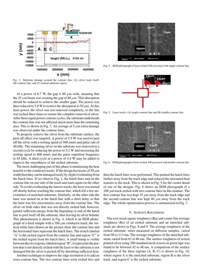
Fig. 5. Laser tracks: (A) single contour line and (B) double contour line.
Fig. 6. SEM photograph of laser etched 100�m track with double contour line.
then the hatch lines were performed. This pushed the hatch linesfurther away from the track edge and reduced the unwanted heattransfer to the track. This is shown in Fig. 5 for the corner detailof one of the designs. Fig. 6 shows an SEM photograph of a100 m track etched with two contour lines in this manner. Thefirst contour line was kept 25 m away from the track edge andthe second contour line was kept 40 m away from the trackedge. The whole optimization process is summarized in Fig. 7.
V. SURFACE ROUGHNESS
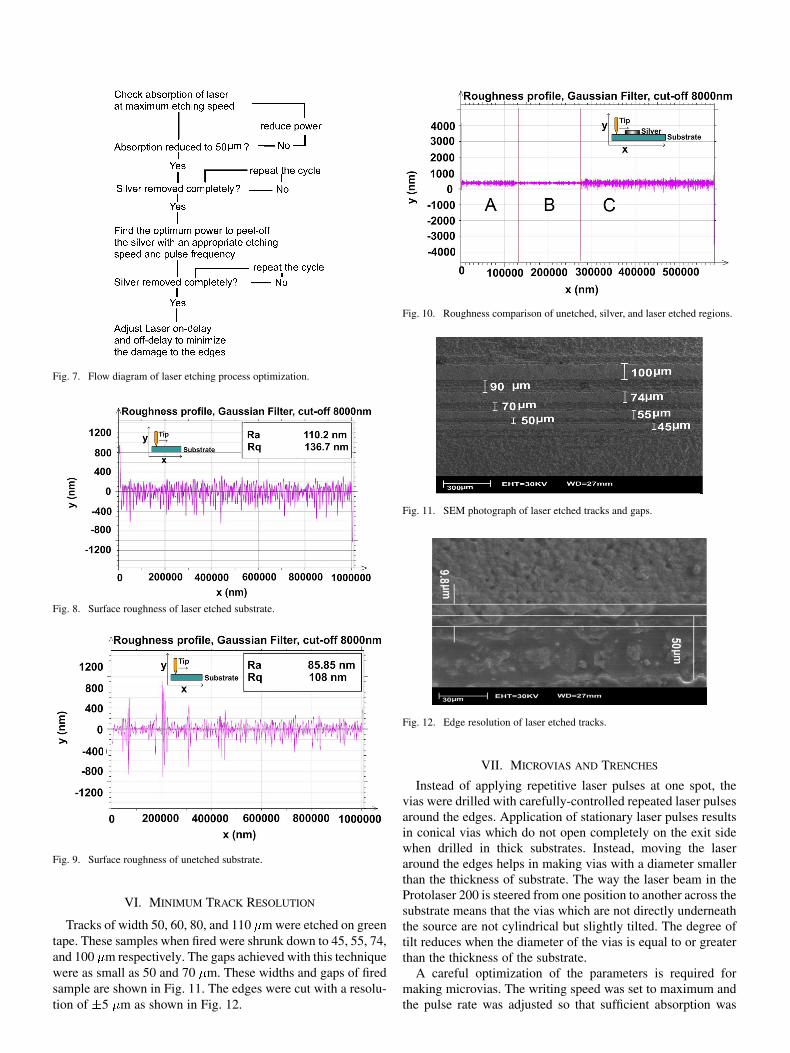
The root mean square roughness (Rq) and center line averageroughness (Ra) of an etched substrate and an unetched sub-strate are shown in Figs. 8 and 9. The average roughness of theetched substrate, when measured on different samples, variedfrom 98 to 113 nm. The average roughness of the unetched sub-strate varied from 61 to 86 nm. The surface roughness of screenprinted silver using 280 standard mesh screen on green tape wasfound to be between 42 to 48 nm. A comparison of the surfaceroughness of the three regions (A, B, C) is shown in Fig. 10,where region A is the unetched substrate, region B is the silvertrack, and region C is the etched substrate.
3258 IEEE TRANSACTIONS ON MICROWAVE THEORY AND TECHNIQUES, VOL. 57, NO. 12, DECEMBER 2009
Fig. 7. Flow diagram of laser etching process optimization.
Fig. 8. Surface roughness of laser etched substrate.
Fig. 9. Surface roughness of unetched substrate.
VI. MINIMUM TRACK RESOLUTION
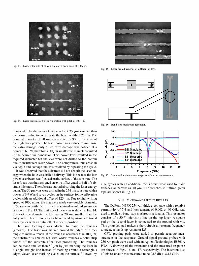
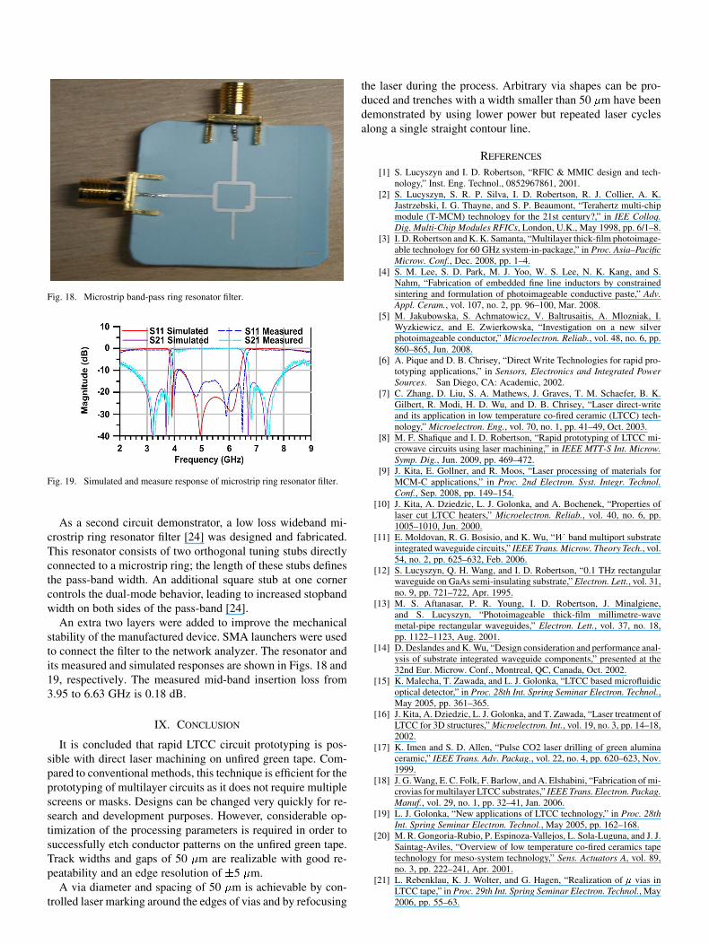
Tracks of width 50, 60, 80, and 110 m were etched on greentape. These samples when fired were shrunk down to 45, 55, 74,and 100 m respectively. The gaps achieved with this techniquewere as small as 50 and 70 m. These widths and gaps of firedsample are shown in Fig. 11. The edges were cut with a resolu-tion of 5 m as shown in Fig. 12.
Fig. 10. Roughness comparison of unetched, silver, and laser etched regions.
Fig. 11. SEM photograph of laser etched tracks and gaps.
Fig. 12. Edge resolution of laser etched tracks.
VII. MICROVIAS AND TRENCHES
Instead of applying repetitive laser pulses at one spot, thevias were drilled with carefully-controlled repeated laser pulsesaround the edges. Application of stationary laser pulses resultsin conical vias which do not open completely on the exit sidewhen drilled in thick substrates. Instead, moving the laseraround the edges helps in making vias with a diameter smallerthan the thickness of substrate. The way the laser beam in theProtolaser 200 is steered from one position to another across thesubstrate means that the vias which are not directly underneaththe source are not cylindrical but slightly tilted. The degree oftilt reduces when the diameter of the vias is equal to or greaterthan the thickness of the substrate.
A careful optimization of the parameters is required formaking microvias. The writing speed was set to maximum andthe pulse rate was adjusted so that sufficient absorption was
SHAFIQUE et al.: LASER PROTOTYPING OF MICROWAVE CIRCUITS IN LTCC TECHNOLOGY 3259
Fig. 13. Laser entry side of 50 �m via matrix with pitch of 100 �m.
Fig. 14. Laser exit side of 50 �m via matrix with pitch of 100 �m.
observed. The diameter of via was kept 25 m smaller thanthe desired value to compensate the beam width of 25 m. Thenominal diameter of 50 m via resulted in 90 m because ofthe high laser power. The laser power was reduce to minimizethe extra damage, only 5 m extra damage was noticed at apower of 6.9 W, therefore a 30 m smaller via diameter resultedin the desired via dimension. This power level resulted in therequired diameter but the vias were not drilled to the bottomdue to insufficient laser power. The compromise thus arose invia depth and damage and was resolved by repeating the cycle.
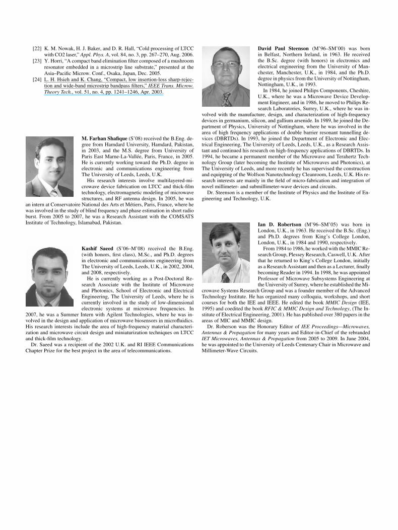
It was observed that the substrate did not absorb the laser en-ergy when the hole was drilled halfway. This is because the lowpower laser beam was focused on the surface of the substrate. Thelaser focus was thus assigned an extra offset equal to half of sub-strate thickness. The substrate started absorbing the laser energyagain. The 50 m vias were drilled in the 254 m substrate with apower of 6.9 W and seven cycles on the surface, followed by ninecycles with an additional offset of 125 m. Due to high writingspeed of 1000 mm/s, the vias were made very quickly. A matrixof 50 m vias, with 100 m pitch, machined in unfired green tapeis shown in Fig. 13. The exit side of these vias is shown in Fig. 14.The exit side diameter of the vias is 20 m smaller than theentry side. This difference can be reduced by using additionallaser cycles with an extra offset in focus position.
The same technique was adopted to make the trenches(grooves). The laser was marked around the edges of a rec-tangle to make a trench. If the trench is narrower than 100 m,the substrate is ablated but with wider trenches a solid stripcomes off the substrate after laser processing. The trenchescan be made smaller than 50 m by just marking the laser ina single straight line instead of marking around a rectangle’sedges. Seven laser marking cycles on the surface followed by
Fig. 15. Laser drilled trenches of different widths.
Fig. 16. Band-stop mushroom resonator.
Fig. 17. Simulated and measured response of mushroom resonator.
nine cycles with an additional focus offset were used to maketrenches as narrow as 30 m. The trenches in unfired greentape are shown in Fig. 15.
VIII. MICROWAVE CIRCUIT RESULTS
The DuPont 943PX 254 m thick green tape with a relativepermittivity of 7.4 and loss tangent of 0.002 at 40 GHz wasused to realize a band-stop mushroom resonator. This resonatorconsists of a 50 microstrip line on the top layer. A squarepad on the second layer is connected to the ground with via.This grounded pad makes a short circuit at resonant frequencyto create a bandstop resonator [23].
CPW probing pads were added to permit accurate mea-surement of the response. Ground-signal-ground probes with250 m pitch were used with an Agilent Technologies E8361APNA. A drawing of the resonator and the measured responseare shown in Figs. 16 and 17, respectively. The insertion lossof this resonator was measured to be 0.83 dB at 8.18 GHz.
3260 IEEE TRANSACTIONS ON MICROWAVE THEORY AND TECHNIQUES, VOL. 57, NO. 12, DECEMBER 2009
Fig. 18. Microstrip band-pass ring resonator filter.
Fig. 19. Simulated and measure response of microstrip ring resonator filter.
As a second circuit demonstrator, a low loss wideband mi-crostrip ring resonator filter [24] was designed and fabricated.This resonator consists of two orthogonal tuning stubs directlyconnected to a microstrip ring; the length of these stubs definesthe pass-band width. An additional square stub at one cornercontrols the dual-mode behavior, leading to increased stopbandwidth on both sides of the pass-band [24].
An extra two layers were added to improve the mechanicalstability of the manufactured device. SMA launchers were usedto connect the filter to the network analyzer. The resonator andits measured and simulated responses are shown in Figs. 18 and19, respectively. The measured mid-band insertion loss from3.95 to 6.63 GHz is 0.18 dB.
IX. CONCLUSION
It is concluded that rapid LTCC circuit prototyping is pos-sible with direct laser machining on unfired green tape. Com-pared to conventional methods, this technique is efficient for theprototyping of multilayer circuits as it does not require multiplescreens or masks. Designs can be changed very quickly for re-search and development purposes. However, considerable op-timization of the processing parameters is required in order tosuccessfully etch conductor patterns on the unfired green tape.Track widths and gaps of 50 m are realizable with good re-peatability and an edge resolution of 5 m.
A via diameter and spacing of 50 m is achievable by con-trolled laser marking around the edges of vias and by refocusing
the laser during the process. Arbitrary via shapes can be pro-duced and trenches with a width smaller than 50 m have beendemonstrated by using lower power but repeated laser cyclesalong a single straight contour line.
REFERENCES
[1] S. Lucyszyn and I. D. Robertson, “RFIC & MMIC design and tech-nology,” Inst. Eng. Technol., 0852967861, 2001.
[2] S. Lucyszyn, S. R. P. Silva, I. D. Robertson, R. J. Collier, A. K.Jastrzebski, I. G. Thayne, and S. P. Beaumont, “Terahertz multi-chipmodule (T-MCM) technology for the 21st century?,” in IEE Colloq.Dig. Multi-Chip Modules RFICs, London, U.K., May 1998, pp. 6/1–8.
[3] I. D. Robertson and K. K. Samanta, “Multilayer thick-film photoimage-able technology for 60 GHz system-in-package,” in Proc. Asia–PacificMicrow. Conf., Dec. 2008, pp. 1–4.
[4] S. M. Lee, S. D. Park, M. J. Yoo, W. S. Lee, N. K. Kang, and S.Nahm, “Fabrication of embedded fine line inductors by constrainedsintering and formulation of photoimageable conductive paste,” Adv.Appl. Ceram., vol. 107, no. 2, pp. 96–100, Mar. 2008.
[5] M. Jakubowska, S. Achmatowicz, V. Baltrusaitis, A. Mlozniak, I.Wyzkiewicz, and E. Zwierkowska, “Investigation on a new silverphotoimageable conductor,” Microelectron. Reliab., vol. 48, no. 6, pp.860–865, Jun. 2008.
[6] A. Pique and D. B. Chrisey, “Direct Write Technologies for rapid pro-totyping applications,” in Sensors, Electronics and Integrated PowerSources. San Diego, CA: Academic, 2002.
[7] C. Zhang, D. Liu, S. A. Mathews, J. Graves, T. M. Schaefer, B. K.Gilbert, R. Modi, H. D. Wu, and D. B. Chrisey, “Laser direct-writeand its application in low temperature co-fired ceramic (LTCC) tech-nology,” Microelectron. Eng., vol. 70, no. 1, pp. 41–49, Oct. 2003.
[8] M. F. Shafique and I. D. Robertson, “Rapid prototyping of LTCC mi-crowave circuits using laser machining,” in IEEE MTT-S Int. Microw.Symp. Dig., Jun. 2009, pp. 469–472.
[9] J. Kita, E. Gollner, and R. Moos, “Laser processing of materials forMCM-C applications,” in Proc. 2nd Electron. Syst. Integr. Technol.Conf., Sep. 2008, pp. 149–154.
[10] J. Kita, A. Dziedzic, L. J. Golonka, and A. Bochenek, “Properties oflaser cut LTCC heaters,” Microelectron. Reliab., vol. 40, no. 6, pp.1005–1010, Jun. 2000.
[11] E. Moldovan, R. G. Bosisio, and K. Wu, “� band multiport substrateintegrated waveguide circuits,” IEEE Trans. Microw. Theory Tech., vol.54, no. 2, pp. 625–632, Feb. 2006.
[12] S. Lucyszyn, Q. H. Wang, and I. D. Robertson, “0.1 THz rectangularwaveguide on GaAs semi-insulating substrate,” Electron. Lett., vol. 31,no. 9, pp. 721–722, Apr. 1995.
[13] M. S. Aftanasar, P. R. Young, I. D. Robertson, J. Minalgiene,and S. Lucyszyn, “Photoimageable thick-film millimetre-wavemetal-pipe rectangular waveguides,” Electron. Lett., vol. 37, no. 18,pp. 1122–1123, Aug. 2001.
[14] D. Deslandes and K. Wu, “Design consideration and performance anal-ysis of substrate integrated waveguide components,” presented at the32nd Eur. Microw. Conf., Montreal, QC, Canada, Oct. 2002.
[15] K. Malecha, T. Zawada, and L. J. Golonka, “LTCC based microfluidicoptical detector,” in Proc. 28th Int. Spring Seminar Electron. Technol.,May 2005, pp. 361–365.
[16] J. Kita, A. Dziedzic, L. J. Golonka, and T. Zawada, “Laser treatment ofLTCC for 3D structures,” Microelectron. Int., vol. 19, no. 3, pp. 14–18,2002.
[17] K. Imen and S. D. Allen, “Pulse CO2 laser drilling of green aluminaceramic,” IEEE Trans. Adv. Packag., vol. 22, no. 4, pp. 620–623, Nov.1999.
[18] J. G. Wang, E. C. Folk, F. Barlow, and A. Elshabini, “Fabrication of mi-crovias for multilayer LTCC substrates,” IEEE Trans. Electron. Packag.Manuf., vol. 29, no. 1, pp. 32–41, Jan. 2006.
[19] L. J. Golonka, “New applications of LTCC technology,” in Proc. 28thInt. Spring Seminar Electron. Technol., May 2005, pp. 162–168.
[20] M. R. Gongoria-Rubio, P. Espinoza-Vallejos, L. Sola-Luguna, and J. J.Saintag-Aviles, “Overview of low temperature co-fired ceramics tapetechnology for meso-system technology,” Sens. Actuators A, vol. 89,no. 3, pp. 222–241, Apr. 2001.
[21] L. Rebenklau, K. J. Wolter, and G. Hagen, “Realization of � vias inLTCC tape,” in Proc. 29th Int. Spring Seminar Electron. Technol., May2006, pp. 55–63.
SHAFIQUE et al.: LASER PROTOTYPING OF MICROWAVE CIRCUITS IN LTCC TECHNOLOGY 3261
[22] K. M. Nowak, H. J. Baker, and D. R. Hall, “Cold processing of LTCCwith CO2 laser,” Appl. Phys. A, vol. 84, no. 3, pp. 267–270, Aug. 2006.
[23] Y. Horri, “A compact band elimination filter composed of a mushroomresonator embedded in a microstrip line substrate,” presented at theAsia–Pacific Microw. Conf., Osaka, Japan, Dec. 2005.
[24] L. H. Hsieh and K. Chang, “Compact, low insertion-loss sharp-rejec-tion and wide-band microstrip bandpass filters,” IEEE Trans. Microw.Theory Tech., vol. 51, no. 4, pp. 1241–1246, Apr. 2003.
M. Farhan Shafique (S’08) received the B.Eng. de-gree from Hamdard University, Hamdard, Pakistan,in 2003, and the M.S. degree from University ofParis East Marne-La-Vallée, Paris, France, in 2005.He is currently working toward the Ph.D. degree inelectronic and communications engineering fromThe University of Leeds, Leeds, U.K.
His research interests involve multilayered-mi-crowave device fabrication on LTCC and thick-filmtechnology, electromagnetic modeling of microwavestructures, and RF antenna design. In 2005, he was
an intern at Conservatoire National des Arts et Métiers, Paris, France, where hewas involved in the study of blind frequency and phase estimation in short radioburst. From 2005 to 2007, he was a Research Assistant with the COMSATSInstitute of Technology, Islamabad, Pakistan.
Kashif Saeed (S’06–M’08) received the B.Eng.(with honors, first class), M.Sc., and Ph.D. degreesin electronic and communications engineering fromThe University of Leeds, Leeds, U.K., in 2002, 2004,and 2008, respectively.
He is currently working as a Post-Doctoral Re-search Associate with the Institute of Microwaveand Photonics, School of Electronic and ElectricalEngineering, The University of Leeds, where he iscurrently involved in the study of low-dimensionalelectronic systems at microwave frequencies. In
2007, he was a Summer Intern with Agilent Technologies, where he was in-volved in the design and application of microwave biosensors in microfluidics.His research interests include the area of high-frequency material characteri-zation and microwave circuit design and miniaturization techniques on LTCCand thick-film technology.
Dr. Saeed was a recipient of the 2002 U.K. and RI IEEE CommunicationsChapter Prize for the best project in the area of telecommunications.
David Paul Steenson (M’96–SM’00) was bornin Belfast, Northern Ireland, in 1963. He receivedthe B.Sc. degree (with honors) in electronics andelectrical engineering from the University of Man-chester, Manchester, U.K., in 1984, and the Ph.D.degree in physics from the University of Nottingham,Nottingham, U.K., in 1993.
In 1984, he joined Philips Components, Cheshire,U.K., where he was a Microwave Device Develop-ment Engineer, and in 1986, he moved to Philips Re-search Laboratories, Surrey, U.K., where he was in-
volved with the manufacture, design, and characterization of high-frequencydevices in germanium, silicon, and gallium arsenide. In 1989, he joined the De-partment of Physics, University of Nottingham, where he was involved in thearea of high frequency applications of double barrier resonant tunnelling de-vices (DBRTDs). In 1993, he joined the Department of Electronic and Elec-trical Engineering, The University of Leeds, Leeds, U.K., as a Research Assis-tant and continued his research on high-frequency applications of DBRTDs. In1994, he became a permanent member of the Microwave and Terahertz Tech-nology Group (later becoming the Institute of Microwaves and Photonics), atThe University of Leeds, and more recently he has supervised the constructionand equipping of the Wolfson Nanotechnology Cleanroom, Leeds, U.K. His re-search interests are mainly in the field of micro-fabrication and integration ofnovel millimeter- and submillimeter-wave devices and circuits.
Dr. Steenson is a member of the Institute of Physics and the Institute of En-gineering and Technology, U.K.
Ian D. Robertson (M’96–SM’05) was born inLondon, U.K., in 1963. He received the B.Sc. (Eng.)and Ph.D. degrees from King’s College London,London, U.K., in 1984 and 1990, respectively.
From 1984 to 1986, he worked with the MMIC Re-search Group, Plessey Research, Caswell, U.K. Afterthat he returned to King’s College London, initiallyas a Research Assistant and then as a Lecturer, finallybecoming Reader in 1994. In 1998, he was appointedProfessor of Microwave Subsystems Engineering atthe University of Surrey, where he established the Mi-
crowave Systems Research Group and was a founder member of the AdvancedTechnology Institute. He has organized many colloquia, workshops, and shortcourses for both the IEE and IEEE. He edited the book MMIC Design (IEE,1995) and coedited the book RFIC & MMIC Design and Technology, (The In-stitute of Electrical Engineering, 2001). He has published over 380 papers in theareas of MIC and MMIC design.
Dr. Roberson was the Honorary Editor of IEE Proceedings—Microwaves,Antennas & Propagation for many years and Editor-in-Chief of the rebrandedIET Microwaves, Antennas & Propagation from 2005 to 2009. In June 2004,he was appointed to the University of Leeds Centenary Chair in Microwave andMillimeter-Wave Circuits.
Related Documents