HARTING Mitronics www.HARTING-Mitronics.com Dr. Christian Goth Phone +49 911 5302 9096 Email [email protected] Dr. Michael Römer Phone +41 32 3442 186 Email [email protected] 1 Laser direct structuring and two- component injection molding for MID series production Dr. Christian Goth and Dr. Michael Römer HARTING Mitronics offers the entire, complete value chain for 3D-MID technologies from a single source. This means that customers will find all process steps at one single location, from the development through to series production of customer-specific products. This approach helps to minimize the number of logistics interfaces, reduce costs and guarantee the quality level of multifunctional MID packages. HARTING Mitronics manufactures the mechanical molded part and the structure of the conductive pattern with single-component injection molding and laser direct structuring or by way of two-component injection molding. Fundamental criteria for selecting the technology are the minimum structure size, the 3D design (2D, 2.5D or n*2D or 3D), the particular requirements placed on design flexibility, and the relationship between investment and component costs. 1 Laser direct structuring In laser direct structuring, a specific change is brought about in the surface of a thermoplastic molded part produced in single-component injection molding. The areas that are activated by the laser can then be selectively metallized (Figure 1 and 2). Figure 1: Sensor platform for a large-format camera, manufactured using LDS technology The injection molded parts, however, must be manufactured from specially doped plastic material with metal- organic connections as an additive.

Welcome message from author
This document is posted to help you gain knowledge. Please leave a comment to let me know what you think about it! Share it to your friends and learn new things together.
Transcript
HARTING Mitronics www.HARTING-Mitronics.com
Dr. Christian Goth Phone +49 911 5302 9096 Email [email protected]
Dr. Michael Römer Phone +41 32 3442 186 Email [email protected]
1
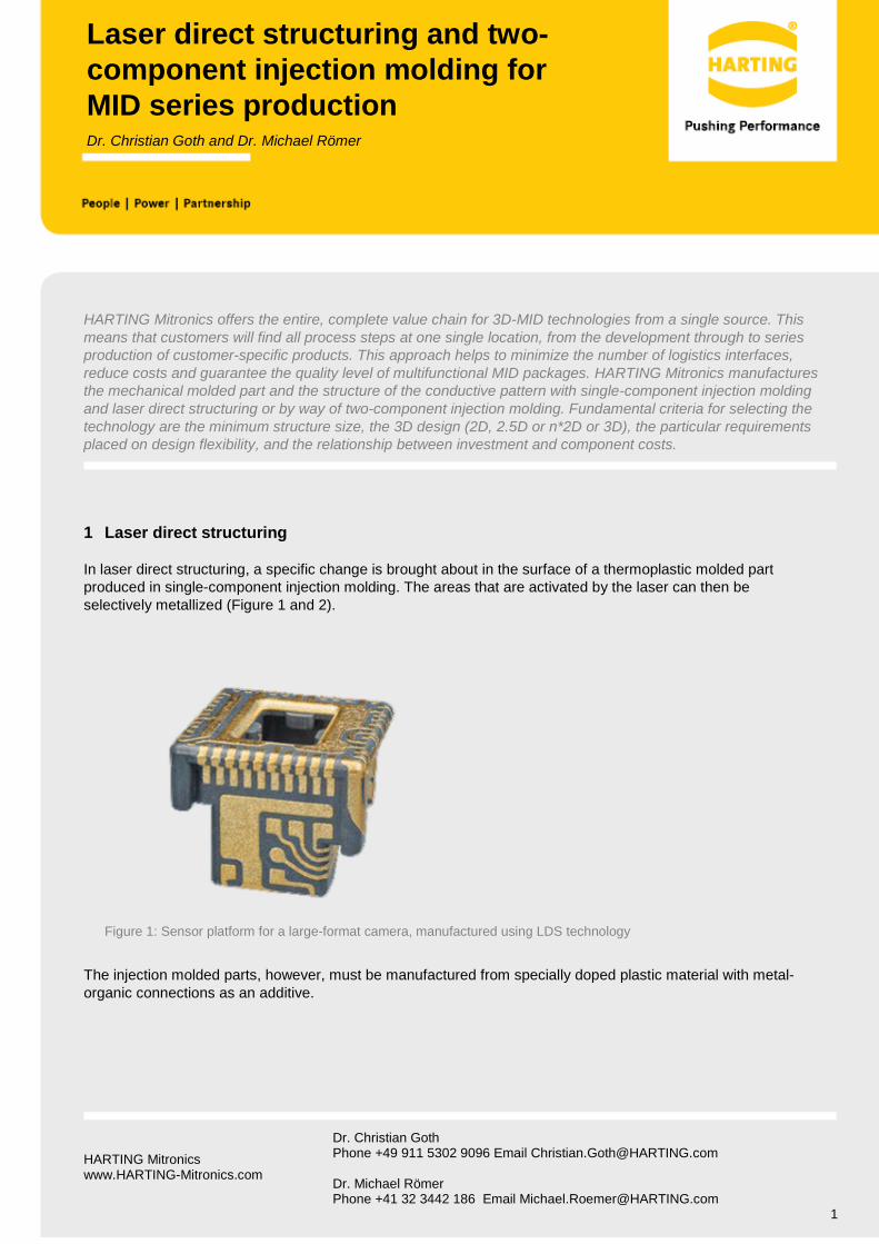
Laser direct structuring and two-component injection molding for MID series production Dr. Christian Goth and Dr. Michael Römer
HARTING Mitronics offers the entire, complete value chain for 3D-MID technologies from a single source. This means that customers will find all process steps at one single location, from the development through to series production of customer-specific products. This approach helps to minimize the number of logistics interfaces, reduce costs and guarantee the quality level of multifunctional MID packages. HARTING Mitronics manufactures the mechanical molded part and the structure of the conductive pattern with single-component injection molding and laser direct structuring or by way of two-component injection molding. Fundamental criteria for selecting the technology are the minimum structure size, the 3D design (2D, 2.5D or n*2D or 3D), the particular requirements placed on design flexibility, and the relationship between investment and component costs.
1 Laser direct structuring
In laser direct structuring, a specific change is brought about in the surface of a thermoplastic molded part produced in single-component injection molding. The areas that are activated by the laser can then be selectively metallized (Figure 1 and 2).
Figure 1: Sensor platform for a large-format camera, manufactured using LDS technology
The injection molded parts, however, must be manufactured from specially doped plastic material with metal-organic connections as an additive.
HARTING Mitronics www.HARTING-Mitronics.com
Dr. Christian Goth Phone +49 911 5302 9096 Email [email protected] Dr. Michael Römer Phone +41 32 3442 186 Email [email protected]
2
Laser direct structuring and two-component injection molding for MID series production Dr. Christian Goth and Dr. Michael Römer
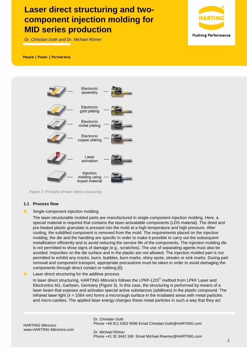
Figure 2: Principle of laser direct structuring
1.1 Process flow Single-component injection molding
The laser-structurable molded parts are manufactured in single-component injection molding. Here, a special material is required that contains the laser-activatable components (LDS material). The dried and pre-heated plastic granulate is pressed into the mold at a high temperature and high pressure. After cooling, the solidified component is removed from the mold. The requirements placed on the injection molding, the die and the handling are specific in order to make it possible to carry out the subsequent metallization efficiently and to avoid reducing the service life of the components. The injection molding die is not permitted to show signs of damage (e.g., scratches). The use of separating agents must also be avoided. Impurities on the die surface and in the plastic are not allowed. The injection molded part is not permitted to exhibit any cracks, burrs, bubbles, burn marks, shiny spots, streaks or sink marks. During part removal and component transport, appropriate precautions must be taken in order to avoid damaging the components through direct contact or rubbing.[6]
Laser direct structuring for the additive process In laser direct structuring, HARTING Mitronics follows the LPKF-LDS® method from LPKF Laser and Electronics AG, Garbsen, Germany (Figure 3). In this case, the structuring is performed by means of a laser beam that exposes and activates special active substances (additives) in the plastic compound. The infrared laser light (λ = 1064 nm) forms a microrough surface in the irradiated areas with metal particles and micro-cavities. The applied laser energy changes these metal particles in such a way that they act
HARTING Mitronics www.HARTING-Mitronics.com
Dr. Christian Goth Phone +49 911 5302 9096 Email [email protected] Dr. Michael Römer Phone +41 32 3442 186 Email [email protected]
3
Laser direct structuring and two-component injection molding for MID series production Dr. Christian Goth and Dr. Michael Römer
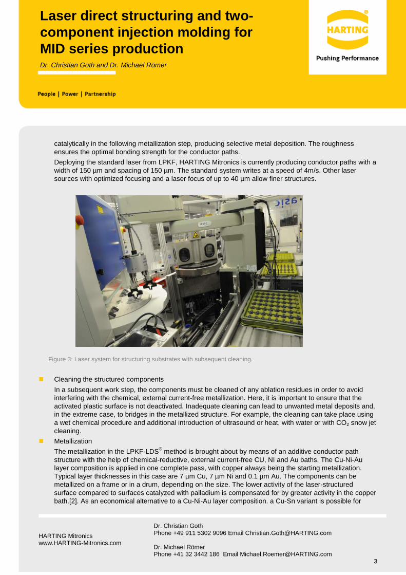
catalytically in the following metallization step, producing selective metal deposition. The roughness ensures the optimal bonding strength for the conductor paths. Deploying the standard laser from LPKF, HARTING Mitronics is currently producing conductor paths with a width of 150 µm and spacing of 150 µm. The standard system writes at a speed of 4m/s. Other laser sources with optimized focusing and a laser focus of up to 40 µm allow finer structures.
Figure 3: Laser system for structuring substrates with subsequent cleaning.
Cleaning the structured components In a subsequent work step, the components must be cleaned of any ablation residues in order to avoid interfering with the chemical, external current-free metallization. Here, it is important to ensure that the activated plastic surface is not deactivated. Inadequate cleaning can lead to unwanted metal deposits and, in the extreme case, to bridges in the metallized structure. For example, the cleaning can take place using a wet chemical procedure and additional introduction of ultrasound or heat, with water or with CO2 snow jet cleaning.
Metallization The metallization in the LPKF-LDS® method is brought about by means of an additive conductor path structure with the help of chemical-reductive, external current-free CU, NI and Au baths. The Cu-Ni-Au layer composition is applied in one complete pass, with copper always being the starting metallization. Typical layer thicknesses in this case are 7 µm Cu, 7 µm Ni and 0.1 µm Au. The components can be metallized on a frame or in a drum, depending on the size. The lower activity of the laser-structured surface compared to surfaces catalyzed with palladium is compensated for by greater activity in the copper bath.[2]. As an economical alternative to a Cu-Ni-Au layer composition. a Cu-Sn variant is possible for
HARTING Mitronics www.HARTING-Mitronics.com
Dr. Christian Goth Phone +49 911 5302 9096 Email [email protected] Dr. Michael Römer Phone +41 32 3442 186 Email [email protected]
4
Laser direct structuring and two-component injection molding for MID series production Dr. Christian Goth and Dr. Michael Römer
manufacturing conductor paths for such uses as safety caps. This variant, however, is only suitable on a limited basis for applications that have to be soldered.
Test and inspection After the metallization, the interconnect device is inspected by means of automatic optical inspection (AOI) for foreign deposits, bridges and breaks in the conductor path. It is furthermore possible to detect cracks in the metallization up to a certain dimension, as well as a delamination of the conductor path in the case of shadow formation.
1.2 Materials for LDS technology
Special doped thermoplastics are needed for laser direct structuring. Metal oxide additives are finely dispersed in a sufficient concentration (4 to 10 weight percent depending on the polymer matrix) and introduced into the material with a stochastic distribution. Thanks to the additives' good temperature resistance, no nucleation occurs while the plastic is processed. Due to the introduced laser energy, the additive, surrounded by an organic matrix, can be activated into a species that is catalytically effective for the subsequent chemical metallization. Laser irradiation causes the polymer molecules to oscillate, as a result of which the molecule chains break apart once a minimum energy has been reached and the polymer matrix is removed (photochemical ablation) or vaporized (relaxation). During the following metallization, which is carried out in chemical copper baths, the exposed and activated additive has a catalytic effect in the irradiated areas, so that the metallization takes place only in the laser-structured areas of the component. The additives do not interfere with the electrical characteristics, nor do they involve any toxic effects and are resistant to extraction. [3] [4]
Numerous amorphous and semi-crystalline plastics for the LDS process are available on the market. The materials can be classified on the basis of their characteristics for the manufacturing process and the later utilization conditions in the field, and also on the basis of the material price. Important material properties here are the processing temperature, the heat distortion temperature, the flowability and the electrical and mechanical characteristics. [3] Complex MIDs that are processed with solder require materials that are suitable for processing in vapor phase or reflow soldering ovens at temperatures from 230 to 260° C. It is necessary to use alternative connection processes with low melting solder or conductive adhesives for materials that are not suitable for these processing temperatures.
An up-to-date overview of the materials especially suitable and released for the LDS process can be found on the homepage of LPKF Laser & Electronics AG (www.lpkf.com). High temperature thermoplastics such as PEEK or LCP, technical materials such as PA, PPA or PET/PBT, and standard plastics such as PC/ABS and also two duroplastic types are available. The materials are developed by LPKF in cooperation with the plastic manufacturers; LPKF tests the metallizability and bonding strength of the metallization. Moreover, HARTING Mitronics carries out intensive qualification of the materials according to the requirements of the particular series application.
1.3 Basic design rules
Comprehensive design guidelines are available at HARTING Mitronics for laser direct structuring; these must be observed during MID design.
The dimensioning of the conductor path widths and spacing is an important point here. Widths of a minimum of 150 µm and spacing of 150 µm have proven themselves in practice and these must be taken into consideration;
HARTING Mitronics www.HARTING-Mitronics.com
Dr. Christian Goth Phone +49 911 5302 9096 Email [email protected] Dr. Michael Römer Phone +41 32 3442 186 Email [email protected]
5
Laser direct structuring and two-component injection molding for MID series production Dr. Christian Goth and Dr. Michael Römer
values less than these are only possible in special cases. The conductor paths here should be designed in such a way that there is no direct contact with the walls. If cost considerations dictate that the component should not be turned during the laser process, the distance to the wall should be greater than 150 µm if the wall inclination is 45°. This distance increases as the angles become steeper. As a rule, a sufficient distance should likewise be provided between the conductor paths and the ejection points, and paths in the area of the injection molded part joint lines should be avoided.
For the component's geometric layout it should be kept in mind that the area the laser is capable of processing is limited by the laser system's scan area. For the LPKF MicroLine-3D 160 Industrial product group, the maximum possible scan field volume is formed by a truncated cone with a base area diameter of 160 mm, a height of 24 mm and an angle of inclination of 77° between the outside surface and the base line. The workpiece can be processed without twisting or displacement within this area. The processing area increases in systems with up to four laser heads in various positions.
The angle of incidence – defined as the angle between the solder of the area that is to be activated and the laser beam – determines the application of energy per surface area. The energy that is distributed across a larger area when the radiation is diagonal must be sufficient to ablate the plastic and activate the additive. A maximum angle of incidence of 60° is therefore recommended. The radius of curvature in this case should be greater than 300 µm in order to avoid sharp-edged transitions. Implementation of through connections with a diameter greater than 300 µm is possible, and an aspect ratio less than 1:1 must be taken into account for one-sided conical bore holes and less than 2:1 for two-sided conical bore holes. Additional detailed design rules can be found in Design Guidelines: MID-LDS. [4]
2 Two-component injection molding
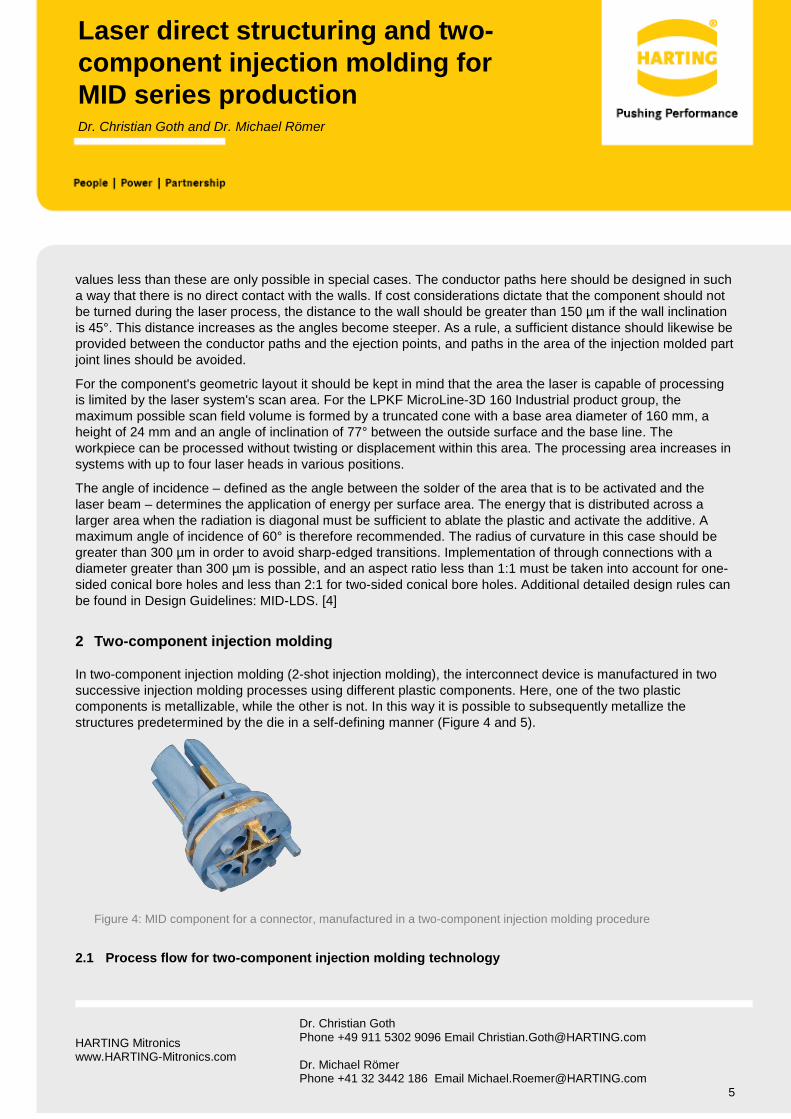
In two-component injection molding (2-shot injection molding), the interconnect device is manufactured in two successive injection molding processes using different plastic components. Here, one of the two plastic components is metallizable, while the other is not. In this way it is possible to subsequently metallize the structures predetermined by the die in a self-defining manner (Figure 4 and 5).
Figure 4: MID component for a connector, manufactured in a two-component injection molding procedure
2.1 Process flow for two-component injection molding technology
HARTING Mitronics www.HARTING-Mitronics.com
Dr. Christian Goth Phone +49 911 5302 9096 Email [email protected] Dr. Michael Römer Phone +41 32 3442 186 Email [email protected]
6
Laser direct structuring and two-component injection molding for MID series production Dr. Christian Goth and Dr. Michael Römer
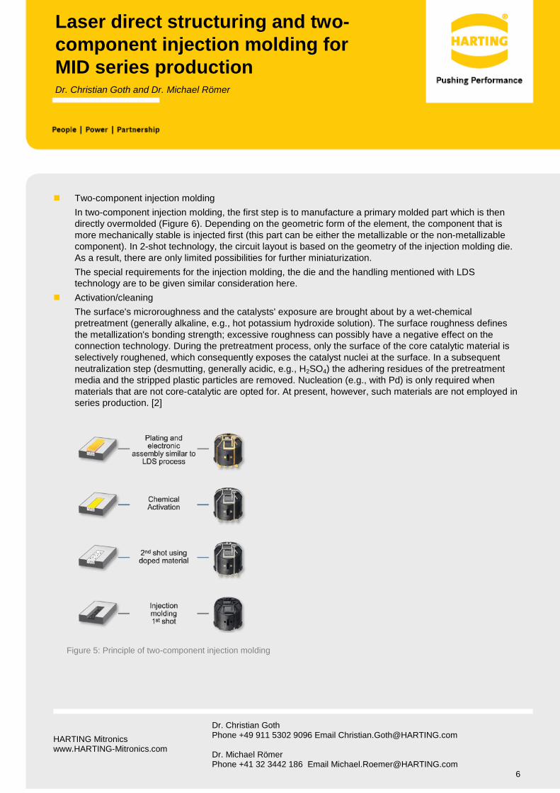
Two-component injection molding In two-component injection molding, the first step is to manufacture a primary molded part which is then directly overmolded (Figure 6). Depending on the geometric form of the element, the component that is more mechanically stable is injected first (this part can be either the metallizable or the non-metallizable component). In 2-shot technology, the circuit layout is based on the geometry of the injection molding die. As a result, there are only limited possibilities for further miniaturization. The special requirements for the injection molding, the die and the handling mentioned with LDS technology are to be given similar consideration here.
Activation/cleaning The surface's microroughness and the catalysts' exposure are brought about by a wet-chemical pretreatment (generally alkaline, e.g., hot potassium hydroxide solution). The surface roughness defines the metallization's bonding strength; excessive roughness can possibly have a negative effect on the connection technology. During the pretreatment process, only the surface of the core catalytic material is selectively roughened, which consequently exposes the catalyst nuclei at the surface. In a subsequent neutralization step (desmutting, generally acidic, e.g., H2SO4) the adhering residues of the pretreatment media and the stripped plastic particles are removed. Nucleation (e.g., with Pd) is only required when materials that are not core-catalytic are opted for. At present, however, such materials are not employed in series production. [2]
Figure 5: Principle of two-component injection molding
HARTING Mitronics www.HARTING-Mitronics.com
Dr. Christian Goth Phone +49 911 5302 9096 Email [email protected] Dr. Michael Römer Phone +41 32 3442 186 Email [email protected]
7
Laser direct structuring and two-component injection molding for MID series production Dr. Christian Goth and Dr. Michael Römer
Metallization In 2-shot technology, the metallization is likewise carried out by means of chemically reductive, external current-free metallization baths. The layer composition, the layer thickness and the process control are comparable to LDS technology.
Test and inspection After the metallization, the interconnect device can be inspected in the same way as with laser direct structuring, namely by means of AOI.
2.2 Materials for two-component injection molding technology
In 2-shot technology, special material combinations are chosen to manufacture MIDs. A catalyst – for example, Pd or Fe – is compounded into one of the two materials. The materials that are employed here must behave differently in the activation and metallization processes.
For series applications, the material combination LCP Vectra® E820i Pd is almost exclusively used in MID technology as the metallizable (meaning core-catalytic) component and LCP Vectra® E130i as the non-metallizable component. Further material combinations are fundamentally available. For cost-efficient applications that do not have to be soldered, the combination PC (e.g., Lexan 121) as the non-metallizable component and PC/ABS (etchable, e.g., Cycolog MC 1300) as the metallizable component is possible, for example. In principle, it must be ensured that the two plastics that are selected have nearly identical coefficients of thermal expansion.
2.3 Basic design rules
HARTING Mitronics has likewise developed comprehensive design guidelines for the design of an MID using two-component injection molding technology. [6]
In two-component injection molding, the conductor paths are implemented by means of the injection molding process. As a result, the attainable conductor path widths and conductor path spacing depend greatly on the material characteristics and the geometry of the molded part. The minimum conductor path width is approximately 300 µm when the minimum conductor path spacing is 300 µm. In 2-shot technology, through connections can likewise be implemented in cylindrical form with a diameter greater than 300 µm; in this case, an aspect ratio of a maximum of 2:1 should be observed. For concave and convex surfaces, the radius of curvature should be at least 300 µm. The component length, width and height should each be in a range between 5 and 40 mm, with special sizes generally being possible.
When an LCP is used in two-component injection molding, it should be noted that the adhesion tendency is low, and therefore a connection should be made between the first and second component by means of appropriate design measures. LCP, however, is a liquid crystal polymer with very good flow characteristics, which means that the material is ideally suitable for miniaturized elements with long flow paths and with thin walls. Additional detailed design rules can be found in Design Guidelines: MID-2-shot.
HARTING Mitronics www.HARTING-Mitronics.com
Dr. Christian Goth Phone +49 911 5302 9096 Email [email protected] Dr. Michael Römer Phone +41 32 3442 186 Email [email protected]
8
Laser direct structuring and two-component injection molding for MID series production Dr. Christian Goth and Dr. Michael Römer
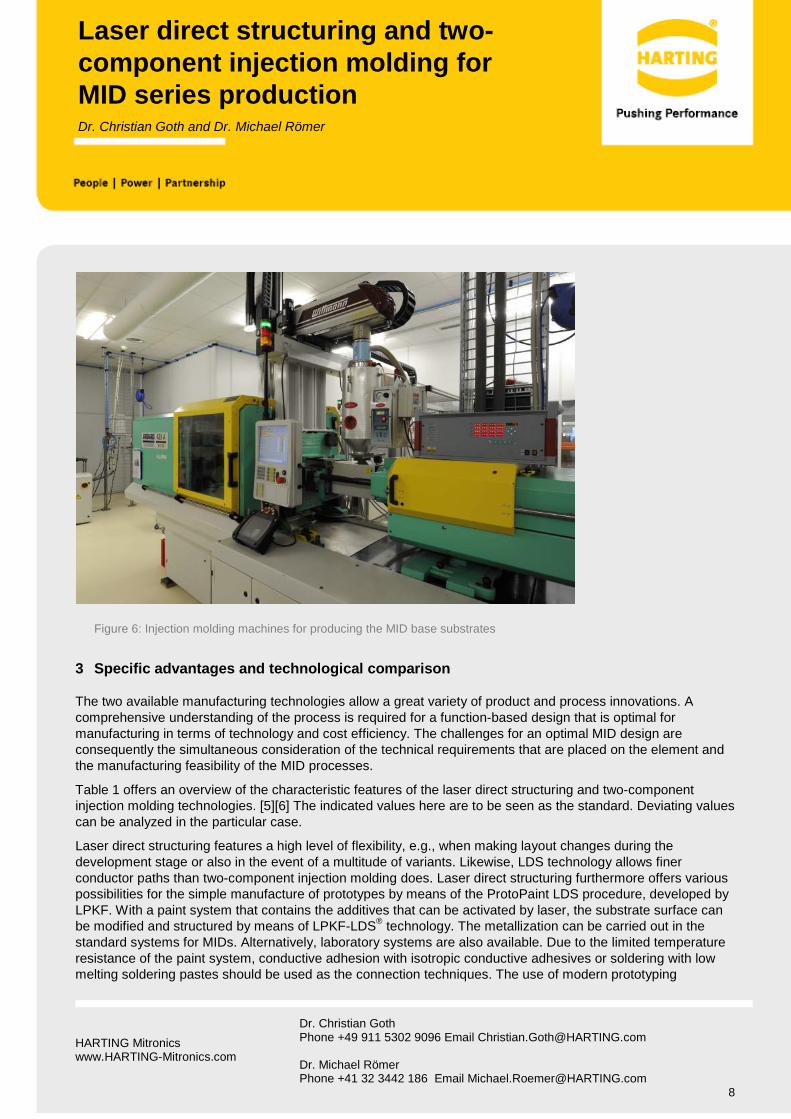
Figure 6: Injection molding machines for producing the MID base substrates
3 Specific advantages and technological comparison
The two available manufacturing technologies allow a great variety of product and process innovations. A comprehensive understanding of the process is required for a function-based design that is optimal for manufacturing in terms of technology and cost efficiency. The challenges for an optimal MID design are consequently the simultaneous consideration of the technical requirements that are placed on the element and the manufacturing feasibility of the MID processes.
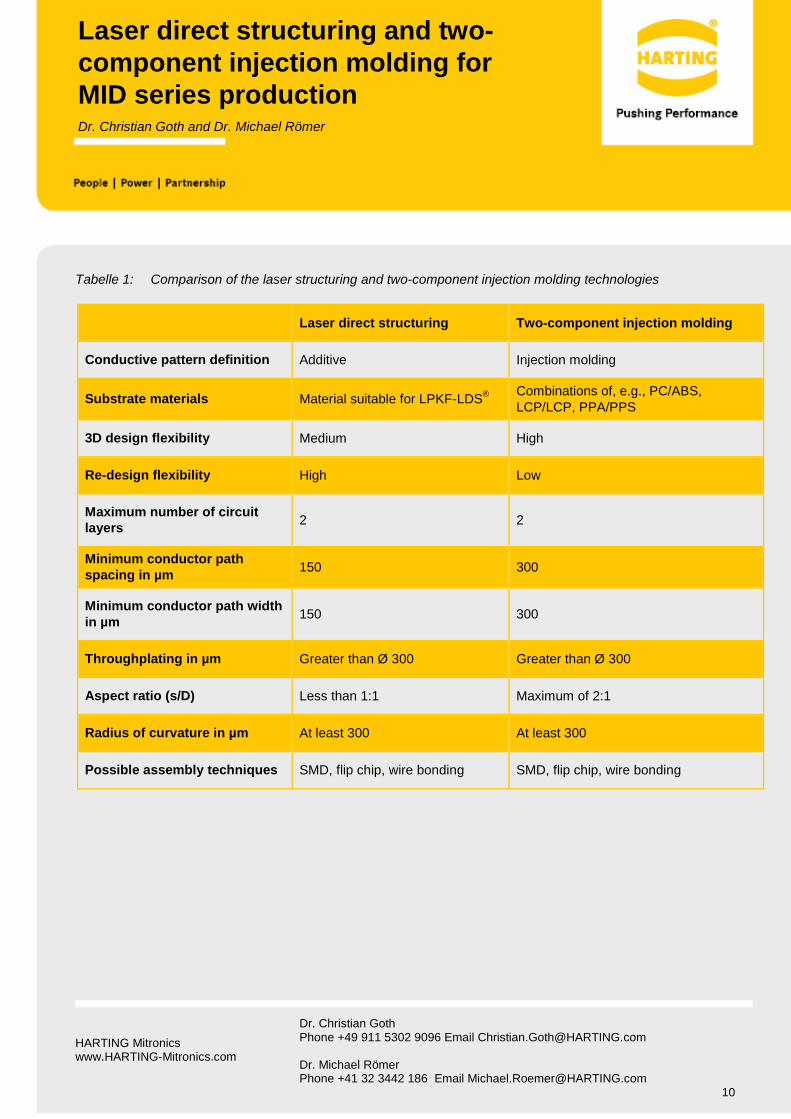
Table 1 offers an overview of the characteristic features of the laser direct structuring and two-component injection molding technologies. [5][6] The indicated values here are to be seen as the standard. Deviating values can be analyzed in the particular case.
Laser direct structuring features a high level of flexibility, e.g., when making layout changes during the development stage or also in the event of a multitude of variants. Likewise, LDS technology allows finer conductor paths than two-component injection molding does. Laser direct structuring furthermore offers various possibilities for the simple manufacture of prototypes by means of the ProtoPaint LDS procedure, developed by LPKF. With a paint system that contains the additives that can be activated by laser, the substrate surface can be modified and structured by means of LPKF-LDS® technology. The metallization can be carried out in the standard systems for MIDs. Alternatively, laboratory systems are also available. Due to the limited temperature resistance of the paint system, conductive adhesion with isotropic conductive adhesives or soldering with low melting soldering pastes should be used as the connection techniques. The use of modern prototyping
HARTING Mitronics www.HARTING-Mitronics.com
Dr. Christian Goth Phone +49 911 5302 9096 Email [email protected] Dr. Michael Römer Phone +41 32 3442 186 Email [email protected]
9
Laser direct structuring and two-component injection molding for MID series production Dr. Christian Goth and Dr. Michael Römer
technologies such as stereolithography, selective laser sintering or fused deposition modeling allows a significant shortening of the development processes. The base body can furthermore also be manufactured by means of the mechanical processing (e.g., milling) of appropriate semi-finished products. When LDS materials are employed, however, the base body must be thoroughly cleaned and chemically deactivated after the mechanical processing in order to avoid external metallizations.
Two-component injection molding allows very flexible 3D design that is virtually independent of the process time. As a result, conductor paths are also possible in cavities and in the area of undercuts that the laser cannot reach due to shadowing effects. Because the structuring takes place during the injection molding, the roughness is considerably less than that in laser structured conductor paths. Wire bonding is consequently possible on the metallized surfaces without further aftertreatment. In LDS interconnect devices, the roughness can be reduced by means of additional measures, such as by using a stamp or by means of a CO2 snow jet.
The electrical characteristics of the two methods differ only slightly due to the identical layer composition and the equal layer thicknesses. The current carrying capacity is determined by the conductor path width due to the limited layer thicknesses of the wet chemical metallization. In general, it should be kept in mind that the conductivity of copper layers that have been purely chemically deposited is only around 60 percent that of solid copper. [7]. A specific resistance 9 x 10⁻⁸ Ωm with typical layer thicknesses on flat structures is the guideline for the Cu-Ni-Au coating system. Larger layer thicknesses are possible with galvanic procedures, in which smoother and harder conductor paths can also be implemented. But in this case, the surfaces that are to be coated must be electrically contacted. Consequently, this may present restrictions for the layout or so-called sacrificial structures may be necessary. [2]
In addition to the exclusive comparison of the technical options, the profitability of the possible alternative solutions should also always be considered. Here, a specific analysis of the particular application is necessary, depending on the complexity and production runs. Due to the fact that the die costs are higher when 2-shot technology is opted for, applications with small production runs use laser direct structuring. For large production runs, the shorter process time for two-component injection molding can be advantageous.
HARTING Mitronics www.HARTING-Mitronics.com
Dr. Christian Goth Phone +49 911 5302 9096 Email [email protected]
Dr. Michael Römer Phone +41 32 3442 186 Email [email protected]
10
Laser direct structuring and two-component injection molding for MID series production Dr. Christian Goth and Dr. Michael Römer
Tabelle 1: Comparison of the laser structuring and two-component injection molding technologies
Laser direct structuring Two-component injection molding
Conductive pattern definition Additive Injection molding
Substrate materials Material suitable for LPKF-LDS® Combinations of, e.g., PC/ABS, LCP/LCP, PPA/PPS
3D design flexibility Medium High
Re-design flexibility High Low
Maximum number of circuit layers 2 2
Minimum conductor path spacing in µm 150 300
Minimum conductor path width in µm 150 300
Throughplating in µm Greater than Ø 300 Greater than Ø 300
Aspect ratio (s/D) Less than 1:1 Maximum of 2:1
Radius of curvature in µm At least 300 At least 300
Possible assembly techniques SMD, flip chip, wire bonding SMD, flip chip, wire bonding
HARTING Mitronics www.HARTING-Mitronics.com
Dr. Christian Goth Phone +49 911 5302 9096 Email [email protected]
Dr. Michael Römer Phone +41 32 3442 186 Email [email protected]
11
Laser direct structuring and two-component injection molding for MID series production Dr. Christian Goth and Dr. Michael Römer
Authors
Dr.-Ing. Christian Goth holds the position of Strategic Technology Manager at HARTING Mitronics. He earned his doctorate at the Universität Erlangen-Nürnberg with a paper on the topic "Analysis and Optimization of the Development and Reliability of Spatial Electronic Interconnect Devices (3D-MID)" under the direction of Prof. Franke in the professorship for manufacturing automation and production systems. From 2007 to 2011 he was executive director of Forschungsvereinigung Räumliche Elektronische Baugruppen 3-D MID e.V.
Dr. Michael Römer has been active as Vice President Sales Europe at HARTING Mitronics since January 2012. Dr. Römer earned his doctorate in inorganic chemistry at the Universität Bielefeld. He is one of the co-founders of Forschungsvereinigung Räumliche Elektronische Baugruppen 3-D MID e.V. in Erlangen, Germany. Dr. Römer worked at various companies such as General Electric Plastics, Hoechst/Ticona and Bosch from 1985 to 2012 as a marketing and sales manager.
Bibliography
[1] BIRKICHT, A.: 3D-MID aus einer Hand: HARTING Mitronics verfügt über die vollständige MID-Prozesskette im eigenen Haus. In: Elektronik – special issue: Räumliche Elektronische Schaltungsträger, 2011, pp. 28-30.
[2] EBERHARDT, W.; WESER, S.; KÜCK, H.: Von der Deko in die Industrie: Metallisierung von MID mit nasschemischen Verfahren. In: Elektronik – special issue: Räumliche Elektronische Schaltungsträger, 2011, pp. 24-27.
[3] FRANKE, J. (PUBLISHER): Räumliche elektronische Baugruppen (3D-MID) – Werkstoffe, Herstellung, Montage und Anwendungen für spritzgegossene Schaltungsträger. Munich: Carl Hanser Verlag, 2013.
[4] HEININGER, N. et al.: Laserbasierte Herstellung multifunktionaler Packages am Beispiel von innovativen Mikrodrehgebern für die Automatisierungs- und Kraftfahrzeugtechnik. http://www.lpkf.de, Zugriff am 08.01.2012.
[5] HARTING MITRONICS (PUBLISHER): Design Guidelines: MID-LDS. Version 1.2, as of 30 Sep. 2009.[6] HARTING MITRONICS (PUBLISHER): Design Guidelines: MID-2K. Version 1.2, as of 30 Sep. 2009.[7] LPKF LASER & Electronics AG (PUBLISHER): LDS-MID Designregeln – Technische Information. Version
2.0, as of Nov. 10, 2010, Garbsen, 2010.
HARTING Mitronics www.HARTING-Mitronics.com
Dr. Christian Goth Phone +49 911 5302 9096 Email [email protected] Dr. Michael Römer Phone +41 32 3442 186 Email [email protected]
12
Laser direct structuring and two-component injection molding for MID series production Dr. Christian Goth and Dr. Michael Römer
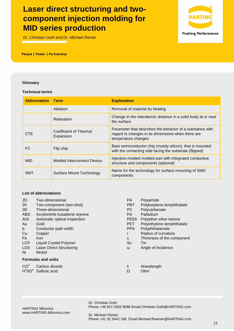
Glossary
Technical terms
Abbreviation Term Explanation
Ablation Removal of material by heating
Relaxation Change in the interatomic distance in a solid body at or near the surface
CTE Coefficient of Thermal Expansion
Parameter that describes the behavior of a substance with regard to changes in its dimensions when there are temperature changes
FC Flip chip Bare semiconductor chip (mostly silicon), that is mounted with the contacting side facing the substrate (flipped)
MID Molded Interconnect Device Injection-molded molded part with integrated conductive structure and components (optional)
SMT Surface Mount Technology Name for the technology for surface mounting of SMD components
List of abbreviations
2D Two-dimensional 2K Two-component (two-shot) 3D Three-dimensional ABS Acrylonitrile butadiene styrene AOI Automatic optical inspection Au Gold b Conductor path width Cu Copper Fe Iron LCP Liquid Crystal Polymer LDS Laser Direct Structuring Ni Nickel
PA Polyamide PBT Polybutylene terephthalate PC Polycarbonate Pd Palladium PEEK Polyether ether ketone PET Polyethylene terephthalate PPA Polyphthalamide r Radius of curvature s Thickness of the component Sn Tin ω Angle of incidence
Formulas and units
CO2 Carbon dioxide H2SO4 Sulfuric acid
λ Wavelength Ω Ohm
Related Documents