LAMPlRAN

Welcome message from author
This document is posted to help you gain knowledge. Please leave a comment to let me know what you think about it! Share it to your friends and learn new things together.
Transcript

LAMPlRAN

LAMPlRAN A
Listing Program
$include(reg51.inc)
org OOh aJmp start
VMotor direction limitA limitB vt danger datatrima
bit pO.O bit pO.l bit pl .6 bit pl.? bit p3 .? bit P 1.0 equ P2
; Program utama
start:
bacadata:
cek2 :
jnb vt,$
mov A,datatrima
cJne A,#OOOOOOOOb,cek2
acall tutup _garasi
cjne A,#OOOOO 1 0 1 b,start
acall buka_garasi
; Prosedur buka garasi
buka _garasi: setb limitA nop nop
;vector interupsi motor
;On Off Motor (O=off, 1 =on) ;arah putar motor (O=tutup, 1 =buka) ;limit switch atas ;hmit switch bawah ;receive enable penerima ;safety detector
;jika remote tidak aktif maka garasi tutup
;aktifkan internal pull-up portl.6
;tunggu 3 IlS

nop jnb limitA,buka
elr Vmotor Jmp start
; prosedur tutup garasi
tutup _garasi: setb danger nop nop nop jb danger ,aHo wed
elr Vmotor
Jmp start
alowed: setb limitB nop nop nop jnb IimitB,tutup
clr Vmotor
Jmp start
tutup: setb Vmotor elr direction Jmp start
, ; prosedur buka pintu garasi
buka:
;jika limit switch belum tertekan maka pintu garasi buka ;jika limit switch tertekan matikan motor ;kembali kelabel start
;prosedur tutup garasi ;aktitkan internal pull-up portl.O
;tunggu 3~s
;jika detector tidak aktif maka tutup garasl ;j ika detector aktif( ada benda yang menghalangi)maka matikan motor ;Iompat kelabel start
;aktitkan internal pull-up portl.7
;tunggu 3~s
;jika limit switch bawah belum tertekan maka tutup pintu garasi ;jika limit switch bawah tertekan maka matikan motor ;Iompat kelabel start
;prosedur tutup pintu garasi ;hidupkan motor ;arahkan putaran motor kekiri(tutup) ;1ompat kelabel start
;prosedur buka pintu garasi

end
setb setb Jmp
Vmotor direction start
;hidupkan motor ;arahkan putaran motor kekanan(buka) ;lompat kelabel start ;akhir program

,~ <' '. '< [' .,:.;.: .... ~- .,-:.~~ .. ........
i "
LAMPlRANB
Gambar Alat ... ,
Bagian Garasi
" ,;1"
. ,
.~~, .. ""
Bagian Mobil (Pemancar)
',. .,.

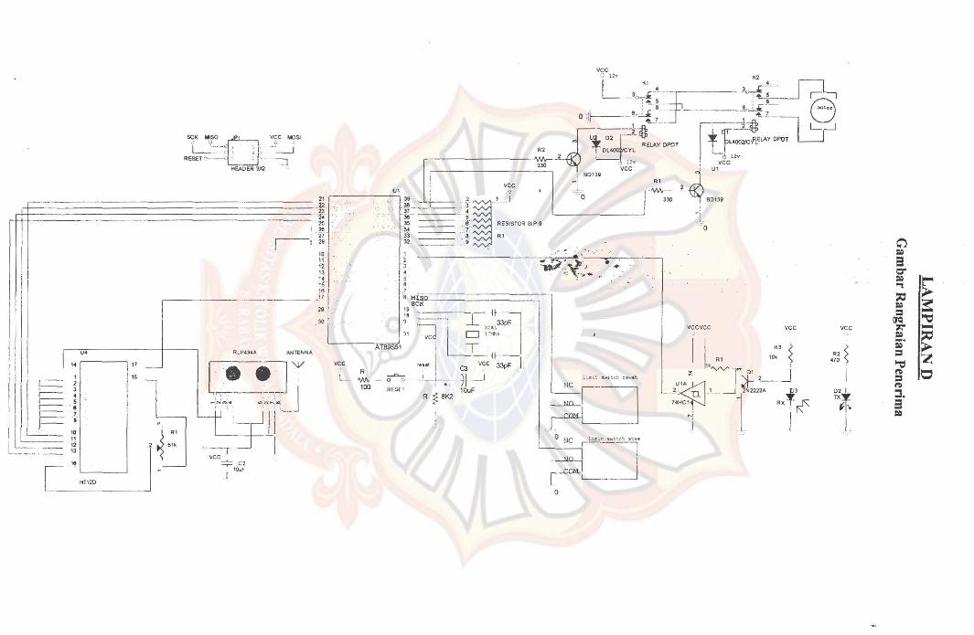
LAMPIRAN C '
Ian Pcmancar Gambar Rangka' -
-J Ul n.~34A
17
VfC SWl L __ ~ .-
1 - ./' -' ~--
I - ~ , _ _ 3 , __ _ 4
__ 5
f-- _6
I -- - ~ : r
"OJ'~ L SW SPDT/SM I
,--~-r--
15 -~~
. I L~f~, c-f::--H-T'-2-E'-O-'P-'8-
.l T 10uF
$C' .. so a L:':::~= ; ~ I~
RESET ~.--~~ :' ;. "- -
vee MOSI _\~.
. -::I HEADER 3)Q
II:
r--:
I
; II i 1:7,'--I
I'J' i17 -.J
I
, !; , -0-' J
\ 1--- .; I[ 0-'
[._:~_I :~L ~ R' _ 1J ~
I '! HT120 r . '"
"
fkP4J .. A ANTENNA
[.~J'V .:~'·n;·-~::H~
,,_,~li vee ~ -, --'--l~F 1
v?[ ... ,,~ .•...... - " .
. ,f-----J?'f~'~~
l,-trL J'1._. ,::{~!::~, It~~:~ : vee I f!9 OD13O vdt .. il " "
i:-=-+- " l~~ , J 10 ,;,:. ... i u"ee
M -- , ,~ ~ 10 ~~ ==-= : RESISTDR s,p , OD'" .. . "' -12 ~ c-:: ' . i~ .. 16 ) :; : LJI;: ~~~i(g_~:;:::_===..l===if-' - =iI
31 "J U ",,33p7l
~ ... - . ...: .. -.. --r-~-~-~.~ .. ~: .. .. -
VCCVCG
I l. R '
vee
Rl ~ lOll < v~ R AlB , " .. , I ~ ':~~---I
l!.Nv......o.... C3VCC 3
I 100 0 0 _.!_ L \) \" 3pF" . RESET ; .-:- 7 .--J
R ~ 8K2 10uF
NC :l",i: ~ .. n~c r. :.". h
~[] • 'VV'J-U1A ' al
... 2_. U , ' ;;t- '-_.. .1 ,,~ ._. .,'2Nm2A RXf'rf I
'0 ~[]H'" ."1,,, ,,.. ? o
vee
R2 ~ 470 ,
I D2 I
"4 J
C') 10> e Q" 10> 5: "1 ,., 10> ~ == IJQ '"C:I );" .... 10>
~ -. 10>
== '"d Z ~ e; == ~ :::!. e :0
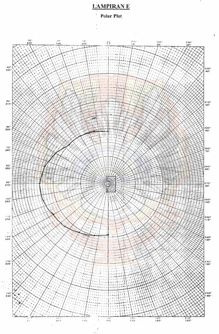
LA.MPlRAN E
Polar Plot

LAMPIRANF
Data Sheet

TLP434A Ultra Small Transmitter
pin' :GND pin 2 : Data In pin:l: Vee "'- U--f@l ~
·-HH pin 4 ; Antenna ( RF output)
-F .. qu ... cy 315,418 .nd 433.112 Mhz
Modulation: ASK Operation Voltage: 2 ·12 vee
Symbol Parameter Conditions Min Typ Max
Vee Operating supply voltage 20 12.0 --
Icc I Peak Curren t (:2V) - 1.64
Icc 2 Peak Current (12V) 19.4
Vh Input High Voltage Idata- 100u/\ (High) Vee-U.S Vee Vcc+().5
VI Input l .ow Voltage Idat"l= 0 uA (I .ow)
FO Absolute Frequency 3 15M hz ",,,Jul. 314.8 3 15
PO RF OutpO! Powcr- SOohm Vee = 9V-12V 16
Vee - 5V-6V 14
DR Data Rate External Encoding 512 4SK "utes : ( Case Temperature = 25°C +- 2°C, Test Load Impedance = 50 ohm)
Application Circuit: Typical Key-chain Transmitter usmg HT12E-1 8DIP, a Binary 12 bit Hncuder t!'om Holtek S.:miconductor Tnc
~ I TlP434A
AD8,9, 10&11 D ala bit or .6.ddress bit
AO·A7 Address bit
Laipac Technology, Inc.
RF outpu l
0.3
31S.2
200 K
105 West Beaver Creek Rd. Unit 207 Richmond Hili Ontario L4B 1C6 Canada Tel: (905)762-1228 Fax: (905)763-1737 e-mail: inli)@luipac.cotn
Unit
V
01/\
mA
V
V
MHz
dBm
dBrn
bps
LAIPAC TECH
RLP434A SAW Based Receiver U.4l1tQ
"'- HI "'~ --.,,, .1 = TTTT 4 ""- • TTfT
pin 1 : Gnd pin 2 : Digital Oata Output pin 3 : linear Output ITnt pin 4: Vee pin 5: Vee pin 6: Gnd pin 7: Gnd pin 8 : Ant.nna
Modulation: ASK Frequency 315,418 .nd 433.112 Mhz SupplyVoltage : 3.3-6.0VDC
Output: Digital & Linear
Symbol Parameter Conditions Min Typ Max
Vee Operating supply vol l agr.: 3.3 S.OV 6.0
Itot Operating Current 45 Vd.ra Data Out Idala = +200 uA ( HIgh) Yl:C-O.S Vee
Idata - -10 uA (I.ow) OJ Electrical Charact~ristics
Characteristics SYM Min I Typ I Max
Operat ion Rad io Frequency I'C 3 15. 418 and 433 .92
Sensit ivity Pref -110
Channel WIdth +-500
Noise Equivalent BW 4
Rlo!cciver Turn On Time 5
Operation Temperature Top -20 80
Baseboard Data Rate 4.8
Application Circuit: Typical RF Receiver usi ng HT12D~ 1 gJ)lP, a Binary 12 hit Decoder with ~ bit ue HT48RXX from Holtel< Semiconductor Inc.
V.hl 5V[lC
Rote
Vuic~/S"~dk~1 .' I P8~ S,eriallntarface ./ roc lilli. Cu,olul PR7
<
U bit ul:
V
mA V
V
Unit
Mil l.
dBm
Khz
Khz
ms
C
KHz

Features
OpcTaring" VOltilge
- 2.4V,-:YV for the H'1'12A - :2.4 V -12V for the HT12E Lcn .. · ~Il)\\~( i-i_Dd hi~:h (u)lSe i(m:ntlf!it.y Cl\.;fOS tL'enrlu;vg)' Lo\\; f.:ihYliihy (';unent. i.i. ; pA \tj'P . ,'u
";.' I"::=;~'-:;'-
HT12A \vith a i:i6kHz carrier for l!lfrared LL1.11fili1jfiSiIJi"I medinHl
Applications
BurgInI' :"-1 h.:r:m system SID0!.;:e and tiTe alarm system Grirage door cc,lltfollt"!'s CnT ell_H)}' con tTolh:'I"'3
General Description
The 212 €llcocie.rs a.re a series efCl\10S LSls for rerfl(IU~ corflYfJl ~y:;.;terfl .3pplic.f11i(jn~ Th(·y ::'if(~
capablt' of eIlI":IJding infi)I'UlatWIl \\"h!rh :..:un::::i:.:::i.s
lOP£" 3iatE3. .i hE prOg7amffiEd addrESSe3/daia
Selection Table
J..IT1 ")l!!l-IT1 ")1= • •• • ~I " ....... -.-
_-f'l _
2'" ~eries of encoders
lVJininlll m tr:'}nsr:nis~ion_ word - FunT '\\'l-'l>d,:, Cor th:, HT i2E - One word for Lhe HTl::!A Bujh-in (I:-;eillf1i (11 f,(~ecb fll-Ih - -'r f8kistOI
Vat-a codl: has pl)SltlVe ~lt':latE"\
IvliT11Tilal e:;;'iSlT:.al LOni.pOllelJ.i~ -,-.~ .
fIT.L2A/S :::UI-' P8.t·i\;1)':;:~
('8.1' nlnrTIl systt'rn Security systeEi C(}n1ie~~ l.!?iephnne:::; either r'!?rnotl:' c:yn1.l"n1 s....,·1:'t( nl:->
upon recpipt. 01 h Trigger .... igIl[tl. The ('.r~rl8hll;1y LL~ ::;;;.dCTL a'T.E LnggcI" UIl (IF.:.' H'T12E UJ." ,t Dc.·\'l'il lTiggf:T f:::'-l the lTT12A further t-:.:.t:.a::'1Cf:5 ~hf: :-:ip
nl~·.\i)Jjjit'- n(J.f-1f:' ;?!.:; ,"f:'{;~.", nF BJiJ'fll~h:"J"';" .in;: r:i..i 1....::;.1 ... <.i.uGlL,ur.i<.i.l1y p~·U·~·jJ.,-'~,,:, <i ;::::3kHL: \.:~,;-
neT fOT ~::.-:::...:.tya.red 3y.:=..tem::.

Block Diagram
TE trigger
HT12E
:~ r)-----..; '~ - .~--.-.~-
,_ : :;O:::~::::::O::O:',",:: .
_._.--- ---c--- '''-c---
DATA trigger
HT12A
',' -, ",-----" , ,--_r __ '_s_r-_:_\i_8t_o_;_-,~ -.-576 Divider ~-"i O~c~~:~~CI~ _
_ CAB ",;---~- • .' ,. t ~
i+-; I;! !
G::<!e Ci .,1 t-Ar c;:.~ ~ 8ir:arv De!ector >--____ _
'---.. ~--~ • .---J
HT12AlHT12E

Pin Assignment
B-Address 4·Dal"
"" rl , . - \, I '
.•• --/ ? .-.\ 1"1-A2Cp :"';::, ~ 4 A._:-1 =,
'-' ,
~Rh\j\::, - !,.,' .--
; (tJ DOiJT , lcp;':~
:~b:-::: , : ...!.p ;",,'~Ym
1'~f-jD~~
a-Address 4-0ata
~"--'! ....
:\i ~ .. /-\2 q4 . " :-1 .
~-'
\ . ...1 l ubr.: :.: ~, ::: b ''':DD 1SPOOUT
i7P~:'i ~:5p :~::;:
1·:,tJD1"
:··.5L-~~ -:3UOiO
.: .. 7Q:7 ;::PDD ·.:"~s~.::: :! tJ D:.::
'-:=:-:--=--~' HT12A
-20 SOP
g·AddreS5 4-AddressfDafa
.~.od ~
A. '~ ~ 2
I\~ q 3 '..,:--1
~!~DoUr 'rEposei :~h :-;~,(:;"l
,_ . ..,,-l ::, ~ 5 T,:::::
.:,:,;~':; -:,b . .:l.,c:;;
,:..~L~:· ~:::~.j:\L}1G
:\:~2 :; O :\O~ \"-SS ~ !; :r: p~:::;.
'---:-::~:--' HTi2E
-18 DiP
8-Address 4·AddresslDala
:'.;::. d ~ C / 20 ~ ~4::. .::..C d ;; : 9 0 '/[.:[:
Ai q::, i8p!')O~J"! A2y 4 i7waSCi
:\? '---: _ ::=: h ~;~:-:J
':'~d; ': ,;:: C 7E
I:..,.~d? ~ ..!b :l.c'df '::"15 C~ f. ::.5 ~ '::',U1\3
;~· ... d ;-: :2f..:..;·'-.o;: \:::;s d ,:; :: p ::":::.~.
'-----', HT12E
-20 SOP
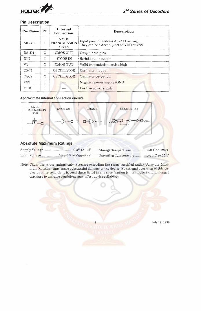
Pin Description
Pin Name ' liO Cnnne~~i:if}n
Description - .. ---... ---".j----t---------- .. '--r----------
/\D;~, . /\.D 1.1.
llOI)'1'
~·.J~:fOS input p~n3 kT sddT2~3 AU--.!:~.7 3~t!inf '-TH :~'\.;S\HSSI(),~I i 1-:6::.e pi:-:~ f .. :'::: r16 e.'-;!.~!T:a.n.;.; :->e:. :'fi Y5~ f:1"
GATt:.:
{HT12Ei
;-1 ,,\10;-:: : TH.A~~Si\'l1S61 Ui'-i
o !
l--'t-:.OT.t.;CTIO;:..: 1 'Tl.':.l: t:>t' l.lE1S t'-:l.r! ;;:.: cx.lt" ·'TJ.lh c.:.1_._ ~.: ) ;'::j2, ryt It,n I)pc~l
Of ODE
(:1\103 OUT
C1\10S IX
:-:1:1::.: ; :-~ f".t1"., ::,: k:'_v
·l'hf"·s(' 1'1l1~ should :Jt' -t'x!.(' tHall.\: ~~t l:J \-'.-::,3 :)1' It'n (l1-lt~l! : ~ se~ :\\)te ,:
i .8:neod(l1' datH so:.tial tnliJ.~m. i 8.iF..:~.! i)utyut .-- --. - -- ._-~ 1. ;-=::d: .:1\:fn:-=-::-~nr;'!:·:i ::-;~:-:f.;-:-::f ... .::_: -:;-: !:-:~ ... -...... t" :'-.::.:1~f·ri(:·-: r:'~.: .
~ Latch: }';Oa tElg vr \. LID ~l(Hl1entary : v:-;s
Aprii Ii. 2000

r ~~ HOLTEK~ i=iT12A!HTi 2E
Pin Name : l!U ' CQn!!e-cti~!!.
Descripiion
I)..~ll-high ~ TranSlll16sion enable, active low {see NotB )
~~-- --~--------------------------------~ OSC1
OSC2
Xl
X?
t-.~7DD
o
-t--
' l~
: V~t'·lHUt.v.i · ~n'pu;.. }iiil
OSC:ILLATOR j : Osciliatr1f output piI:
OSCILLATOR 2 : 455kHz res.onaior oscillator input
OSCIIJ.o/\TOH 2-.. i------.. ----
.-, .•. ~~. ~:: r;.:":::i; ;::::~:-::: ;-:.-;:'-. ;-- ---- ----i I\;,;;;i t ivB prii'i'er ,~ UPP!.Y
Note : DR-Dl1 are Hil d~bllnpllt and t.ransmi~slnn en:-l. bl~ pins oCi.he TIT12:A .
TE 18 a t!'am;mb~i{ln €nnble l-HH of lb(, HT1~E,
Approximaie internal connections
i-..i!i.iOS fRt..NSM!sSlGN
CATE
_. ---.Jrn_, --::J
OSCiLLATOR 2
C~AOS iN
y
~ C~-{~)o---- -·
CMOS OUT
---- -{~X)-{J
NMu::; TRAi,,::;iyii~~iOr .. GA 1 i::
PR.C:TECT~:JN D~C:DE
,_ TTl . ~ - . ---Ii _--.t-.~~
-":8::; ~ ':' -,-
Absolute Maximum Ratings
SlJlJply V,)ll.ng-e (HT12 A:
In pul. Vnh~'qj'
OSCILLATOR ~
CS~·;i C --f0J;;.-....,..-::;·-.. r: ;:1:.K2
: ., : '.--~ ~---.-
~nie : The~e fi re. ~tre.Sf: raLing-:-; rmly. StTP..~~ES exceeding the range specified nnder "Ahsniute ?\:Jax-i.mWl! Ralings" muy caUBe sUDstanLiai damage l o the tievICt'. F uncl!mlal ~Jperall0n 01 lhis U':Vlce a t. ni.. hef conciit-inns beynnd those lis teci in the 5pec'ii1cation is nOl implied and prolonged expo-
r-AA~ HOLTEK~
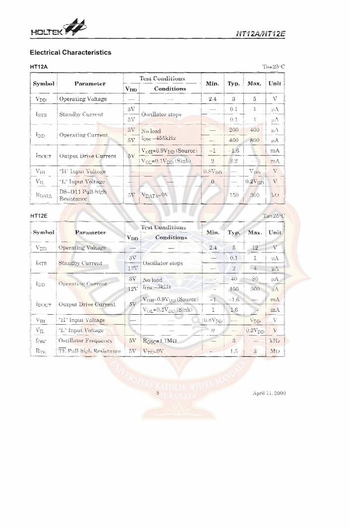
Electrical Characteristics
HT12A
1 Symbol ~
:: i STB
L
Parampier
i Operating Voltage
i Standhy Cl1rre_nt.
~ - -- ----
\ Open~ t.1ng C: uYrer:!.
inOET : Outp ut Drive Curreni
VIff ; "R " In!-iut. \tvh-i-igC' ,~- - - i---- --. . --. - -
HT12E
~ "L" Input. V'Jlt.t-l_ge --T'
DS-Dl l Pull·high j R.et' ist.aIltC
~ SyruboJ ; Panunerer
VDn . Oper a ting Voltage
Standby Current
OUtput Drive Current
t T~<;;i. C;';.i.a1itiuI.i~ f-- -~.--
i Vou ' Conditions
i-- -1---- - ! 3V ~ 1'\ 0 load 1- -----! r f, V i fU:-ic:::455kHz
Min.
2.4
i=iT12A1HTi2E
Typ.
0.1
Max. ' Uni t I 5 v 1 . ~u\ ii
.-:-._-!!
i 0.1 i j P..i.\ ;\ ~: - ----;- . . --!-- ---, -- ':1
20n : 400 p:\ \- ---_ ~--.. -~. - - --+---- -----i:
400 ROO
-1 - 1.6 rnA
3 .2 IIlA
;: LtG __ i _ _ _ - _.'--- --- -;- ---; -- --:- - - -;--.
: von Conditions
3\! .-' ---~ UscillatDT s tops ! l ~i>;l . -
:,v ! 1\0 load
12V : i!~sc-Jkllz
5V
5
- -----i- - --
, - - '
-~:
Min.
2.4
v O.2VDD ; -f -~-- ---:' .i---
1-.0
Ta=25'·t.:
Tn>. ! M"". Coil. ._' - .-~, - - -; - .,-----i',
12 V
0.1 1 ~lA
~\.
80 itA ---1-_ --! -- - ---;- -' --i\
300
. .
-~: -i} ; O.2VDD i V
-: -. -f" --- -- --:;
:=i
April 11. 2000

HT12A1HT12E
Functional Description
Operation The 212 series of e"':{'n~~;y;: ~'=~;: 2. ·1.-"n:.pi t:r?,E! ~~i,:<:"~~'!' ....... T,..lIP '. ~ :Y"~"'" .... ~.:/";~~+ .-..f "': ~""""~~~~, ~<>hn ·~r ,,:;hle (TE for the HT12E . ,. ~:,.: ::~~ :'", "~:',: ::·:·~ "·.,,'.: · .. c ,"" .. . ; ., .: .... , , ', .. ,,' , . .. ' ,.. , .•
- _ " .. "0' -'
transmission eDabh~ :.TE er DH- D11 ) i ~ hdd. -: (;'.~.I , O;H-;e t.b~ tr~n::;.m: ;:;~ ! ;:;!l ~~-~.:::.bl e r :::-tw'n~ : !igh the 8H
coder output compleles :t:-, final eydp. flnd f h~n !$top~ ~!!~ ::.:ho'.-rn heb, .....
iiU -+t I+- < 1 word
Encoder I DDUT ....J
I+- 4 words -+t '-- Transmitted ____ ......-- Continuously . '
Transnrission timing for the HT12F.
; ";;:;-011 x.ey4n 11
-+l I+- < 1 word
I I
E~ JlITIll __ -----'IIIII1I11I1I1I11I1I11II1/"I"III/1"""~ ..;~3BI<~z ca~ -+l I+- 1 word f+-- l",,",=';i;. ----.; !+- 1 _0
1Tansmission timing for the HTl2A (ll~1 !.{=,;;;·-;oflT,1ng or V 1 H))
l I ! .! (oi' d8ta=1)
C " ~ e 1 wcro 14- 7 words ~
E~~~er -.J1IH!!IIIIIIII!lIL "._ .rrrrmllmmlTllIl!!II1I1II1II1I1111111111111 . -+t ,.. 7 words +I f+-- ~;~g~~~:,,:;
1 word (an dala=1)
6 April 11, 2000

HT12AIHT12E
Infr)rrnation word
Ii liMB", ! '.he device is in thelatch mode (for use with the latch type of data decoders). When the transmi:o;si"n enah!e is removed during a transmission. the DOUT pin outputs a complete word and then swiJ;:), OH l.hc oUwr hand, ifI/MR~O Hit' dflvlre i~ in the momf'ntary mod~ (for use with the momentary type of data decoders), 'lVher:. tIl\.: 1.1 w lswitiSfvH \;';: :'ci.Ll\;: ;:;. ... ~~~ . ... .... 1 J -;"": ':i"it;, ~~ L· ;.jil;)l ;.t;~slon, the DOUT outputs a complete word ",,<1 t.!;;:;" ."l<i" 7 wn"h nil with til" "1" data ~,tlde.
An information word consists of 4 periods as ilJlIst.rat.f!d below.
Composition of information
· .~,;·==,.:data waveform
data code period
I !
-..l ,
Each programmable address/data pin can be externally set to one of the following two logic states as shown below.
lose
"One--+ __ ...J
AddresslData bit waveform for the HT12E
lose
.,. "One'"
Data SH l -;.---"Zero"
( "One"
Address Bit ,
' ~Z~ · __ M
.. " ... .. .... . ,.,j , ... -.... ~., 1 i\ ! i ; ! :: i 1·~ 1; ; :,
~ Address Bit .
AddresslData bit waveform for the HTl2A
7 April 11.2000

HOLTEK# HT12A1HT12E
The address/data bits of the HT12A are transmitted with a 38kHz carrier for infrared remote controller flexibility.
Address/data programming (preset)
The status of each address/data pin can be individually pre-set to logic "high" or "low". If a transmission-enable signal is applied, the encoder scans and transmits the status of the 12 bits of address/data serially in the order AO to ADll for the HT12E encoder and AO to Dll for the HTl2A encoder.
During information transmission these bits are transmitted with a preceding synchronization bit. If the· t.rigger signal is not applied, the chip enters the standby mode and consumes a reduced current of Ie" than 1~ for a supply voltage of 5V.
Usual applications preset the addretis pins with individual security codes using DIP switches or PCB wiring, while the data is selected by push buttons or electronic switches.
The following figure shows an application using the HT12E:
The transmitted information is as shown'
! Pilot Is!~
AO r 1 I
Al
o
A2 A3 A4
1 o o
aSCI OSC2
A7
1
8
DOlIT
ADB
1
Transmission medium
AD9
1
ADlO I AD 11
1 I 0
April 11, 2000

HT12A1HT12E
Address/Data sequence
The following provides the address/data sequence table for various models of the 212 series of encoders. The correct device should be selected according to the individual address and data requirements.
AddressIData Bits Part No. I
0 I 1 2 3 i 4 5 6 7 8 9 10 i 11
HTI2A AO Al A2 A3 A4 A5 A6 A7 D8 D9 DIO D11
HT12E AO Al A2 A3 A4 A5 A6 A7 I AD8 AD9 ADI0 AD11
Transmission enable
For the HT12E encoders, transmission is enabled by applying a low signal to the TE pin. For the HTl2Aencoders, transmission is enabled by applying a low signal to one of the data pins DB-Dll.
Two erroneous HT12E application circuits
The HT12E must follow closely the application circuits provided by Holtek (see the "Application circuits") .
• Error: AD8-AD11 pins input voltage> Voo+0.3V
{ aSC2 VDD
~, ~- .~~
ascI ADll
TE AD10
vss AD9
AD8 To
< ~ ~ ~ d ••• <
HT12E Ir T,
9 April 11, 2000

• Error: The Ie's power source is activated by pins AD8-ADll
Flowchart
• HTl2A
No
VDO~-----------,
AD11~------~~v-~~~v-~
AD10~----~1--VVV-'
A09 \--.....,-++-w.--+ AD8~~~-+~NV~
HT12E
• HT12E
No
No
Note: D8-Dll are transmission enables ofthe HTl2A.
TE is the transmission enable of the H'l'12E.
10
HT12A1HT12E
12V
April 11, 2000

HOLTEK#
Oscillator frequency vs supply voltage
lose (SeIII.)
7.00
6.00
4.00
1.00
, - -, - - -
r - - -
.' - - - - - - -' - .
2 3 4 5
HT12A1HT12E
Rose (0 )
.~::..:..~_...;...~_---::--::7"=== 470k
6 7 8 9 10 11 12 13 Voa (V ~C)
The recommended oscillator frequency is foseD (decoder)" 50 fOSCE (HT12E encoder) 1
;: - fOSCE (HTl2Aencoder) 3
11 April 11, 2000

Application Circuits
Voo 1000
Note: Typical infrared diode: EL-IL2 (KODENSHI CORP.)
Typical RF transmitter: JR-220 (JUWA CORP.)
12
HT12A1HT12E
April 11, 2000

Holtek Semiconductor Inc. (H .. ad quart<!ro) No.3, Creation Rd. II, Science-based Industrial Park, Hsinchu, Taiwan, R.O.C. Tel: 886·3·563·1999 Fax: 886·3·563·1189
Holtek Semiconductor Inc. (Taipei Office) I IF, No.576, See.7 Chung Hsiao E. Rd., Taipei, Taiwan, R.O.C. Tel: 886·2·2782·9635 Fax: 886·2·2782·9636 Fax: 886·2·2782· 7128 (International sales hotline)
Holtek Semiconductor (Hong Kong) Ltd. RM.711, Tower 2, Cheung 8ha Wan Plaza, 833 Cheung Sha Wan Rd., Kowloon, Hong Kong Tel: 852·2·74ij·8288 Fax: 852·2·742·8657
Holtek S .. miconductor (Shanghai) Ltd. 7th Floor, Building 2, No.889, Yi Shan Rd., Shanghai, China Tel: 021·6485·5560 Fax: 021·6485·0313
Holmate Technology Corp. 48531 Warm Springs Boulevard, Suite 413, Fremont, CA 94539 Tel: 510·252·9830 Fax: 510-252·9885
Copyright © 2000 by HOLTEK SEMICONDUCTOR INC.
HT12A1HT12E
The information appearing in this Data Sheet is believed to be accurate at the time of publica.tion. Howevor, Holtek assumes no resJXlnsibility arising from the use of the specifications described. The applications mentioned herein are used solely for the purpose of illustration and Holtek makes no warranty or representation that s.uch applications will be suitable without further modification. nor recommends the use of its products for application that may pres· ent a risk to human life due to malfunction or otherwise. Holtek reserves the right to alter its products without prior notification. For the most up·to-date information. please visit our web site at http://www.holtek.com.tw.
13 April 11, 2000

Features
• Operating voltage: 2.4V-12V • Low power and high noise immunity CMOS
lechnology • Low standby current
Capable of decoding 12 bits of information Pair with Hollek's 212 series of encoders Binary address setting Received codes are checked 3 times
Applications
• Burglar alarm system • Smoke and fire a larm system • Garage door conkollers
Car door controllers
General Description 12
The 2 decoders are a series of CMOS LSIs for remole control system applications. They are paired with Holtek's 212 series of encoders (refer to the encoder/decoder CTOSS reference table). For proper operation, a pair of encoder/decoder with the same number of addresses and data format should be chosen.
The decoders receive serial addresses and data from a programmed 212 series of encoders that are transmitted by a carrier using an RF or an IR transmission medium. They compare lhe serial input data three times continuously with
Selection Table
212 Series of Decoders
AddressiData number combination HTI2D: 8 address bits and 4 data bits HT12F: 12 address biLS only
Built·in oscillator needs only 5% resistor Valid transmission indicator Easy interface with an RF or an infrared transmission medium Minimal external components
Car alarm system Security system Cordless lelephones Other remote control syslems
their local addresses. If no error or unmatched codes are found. the input data codes are decoded and then transferred to the output pins. The VT pin also goes high to indica te a valid transmi.ss.ion.
The 212 series of decoders are capable of decoding informations that consist of N bits of address and 12-N bits of data. Of this series, the HT12D is arranged to provide 8 address bits and 4 data bits, and HT12F is used to decode 12 bits of address information .
runction I Address I Data I VT Part No: . ..... I No. i No. I Type !
i Oscillator I i
Trigger , Package I
HT12D 1 8 1 4 L i ~ RC oscillator i DIN active "Hi" ! 18 DlP/20 SOP
HT12F ! 12 ! 0 - I \ : RC oscillator I DIN active "Hi" ' 18 DIP/20 SOP
Noles: Data type: L stands for latch type data output.
V1' can be used as a momentary data output.
,) uly 12, 1999

212 Series of Decoders
Block Diagram
6 : Data o
VT
t t ····6··6 ···· .... ····
Address VoO vss
N oLe: The address/data pins are available in various combina lions (see the address/data table).
Pin Assignment
8-Address 8-Address 12-Address 12-Address 4-Data 4-Data O-Data O-Data
NC NC NC NC
AD VOO AD VOO AD VOO AD VOO A1 VT A1 VT A1 VT A1 VT
A2 OSC1 A2 OSC 1 A2 aSC1 A2 aSC1
A3 a SC2 A3 OSC2 A3 aSe2 A3 aSC2
A4 DIN A4 OIN A4 DIN M OIN
AS 011 AS 0 11 AS A11 AS A11
A6 010 A6 0 10 A6 A10 A6 A10
A7 09 A7 0 9 A7 A9 A7 A9
VSS 08 VSS 08 VSS A8 VSS A8
HT120 HT12F HT12F - 20 SOP -18 DIP - 20 SOP
2 July 12, 1999
212 Series of Decoders
Pin Description
I Pin Name 'I I/O I, , Connection ~ I '-c[c---N- 'M- O-S--+-l AO-All ! I TRANSMISSION Input pins for address AO-All setting I : GATE They can be externa lly set. to VDD or VSS.
Internal Description
! D8-Dll o CMOS OUT Output data pins I --i DIN i I I CMOS IN , Serial data input pin
~ VT ! 0 I CMOS OUT Valid transmission. active high I
! OSCI I I i OSCILLATOR Oscillator input pin
OSC2 i O ( OSCILLATOR ' Oscillator output pin
VSS I : - Negative power supply (GNDI : VDD I I - , Positive power supply
Approximate internal connection circuits
NMOS CMOS OUT CMOS IN OSCILLATOR TRANSMISSION
GATE
--L -----{)o-D o--j)o------ EN~ -- -JT'L-[] OSC1 ~ OSC2
Absolute Maximum Ratings
Supply Voltage .... .......... ..... ........ ... -O.:lV to 13V Storage Temperature ....... -50'C to 125'C
Input Voltage ........ _ ...... ..... Vss- O.3 1.0 VDD+O.3V Operating Temperature ...... .. .. -20"C to 75"C
Note : These are stress ratings only. Stresses exceeding the range specified under "Absolute Maxi · mum Ratings" may cause substantial damage to the device. Functional operation of this de· vice at other conditions beyond those listed in the specification is not implied and prolonged exposure to extreme conditions may affect device reli ability.
3 .I uly 12, 1999
HOLTEK# 212 Series of Decoders
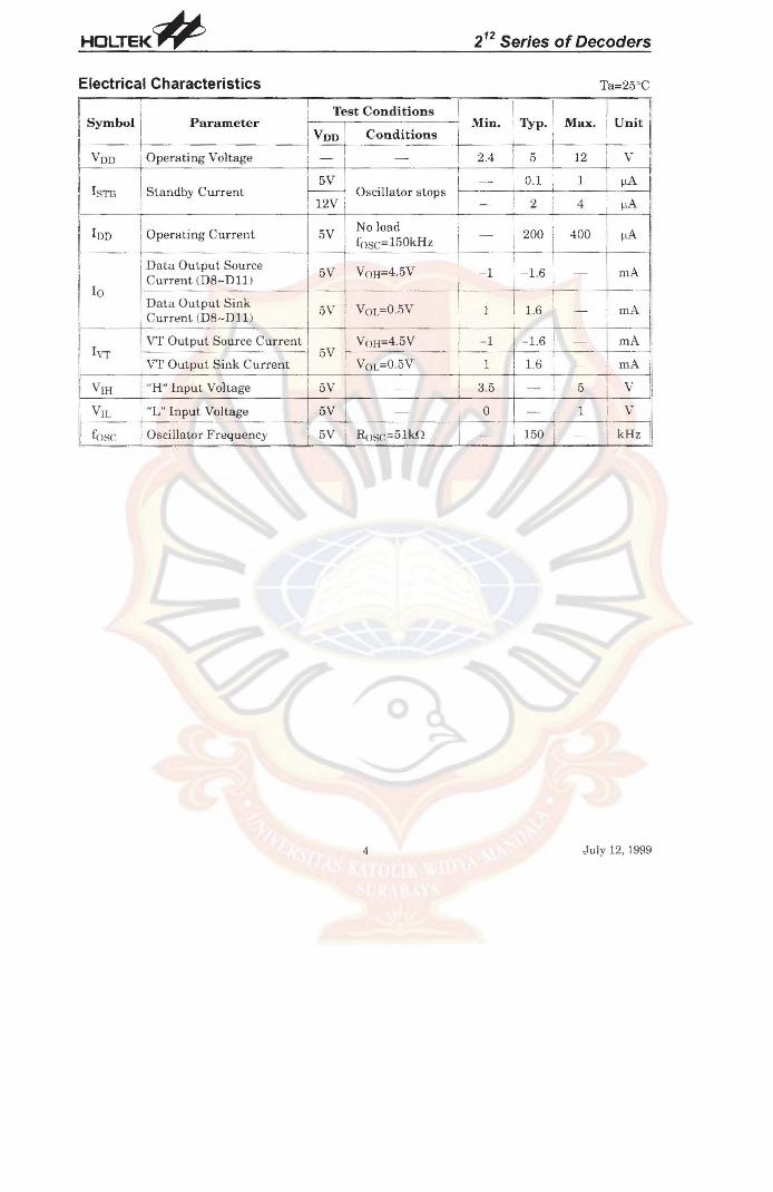
Electrical Characteristics
~ i : Test Conditions I I 11 \ Symbol ! Parameter i VDD ! Conditions Min. I Typ. Max. I Unit II
O t · "] ' . 1 2 4 12 ' \' "I i pera ·lng votage ! - I ' . a
I, I 1 5V ! 0.1 1 ftA II',
~I ISTH I Standby Current I~ Oscillator s tops f-- --:-1~ , 12V i I 2 4 A
1 100 i 0,,,",,,. "."e" I ov 1 8::::;~OkH' + 200 ' 400 I :~ Ii
i Data Out put Source ' 1- - --- ~ I I 10 I Current (DS-DIl) I 5V VOH=4 5V __ + - 1 ~ - l.6 : __ +:~ ! Data Output Smk 5V VOL=O 5V I ~ 16 A I I j Current (DS-DII l I I ' I - , m ~ 1- -l vT Output Source Current ' VOH=45V r-'-'=1i-~l~6I--=-Im'A Ii ~ In ! VT Output Sink Current [ 5V VOL=0.5V I 1 16 i- I rnA I I VIH i "H " Input Voltage ! 5V 1 I 3 5 - I 5 I V
'I V1L "L " Input Voltage I 5V ! 0 1 I V If..· --'~-+_--=-- - -=-·- ----!-I - -+: - - -~--_+-----'----+_--., .. ---i fose Oscillator Frequency i 5V ! Rosr.=51kf! , 150 i kHz "
4 July 12, 1999

HOLTEK#
Functional Description
Operation
Th e 21 2 series of decoders provides va rious combinations of addresses a nd data pins in dilTerent packages so as to pair with the 212 series of encoders .
The decode rs r eceive data that are transmitted by an encoder and interpret the first N bits of code period as addresses and the last 12- N bits as data, where ~ is lhe address code n umber. A signal on I.he DIN pin act. ivates the oscill ator which in turn del..:odes the incoming address and data . The decoders \vi]} then check the rece ived addl'(~.ss th ree t.i mes ('nn t in uonsly. If t,he received address codes all m at<:h the contents of the decodeT'R local addTe~s . the 12-N hits of da tu aTt' ue('mleLl to udivate the ou tput pins and the VT pin is set high to indicate a valid UanSrll ;sf<;.lon. This will 1[1 6\· un less the fHl d rBss code is incorrect or n o signal is received.
Th e output nf t.he VT pin is high only when the t.Tunsmi:;sion is valid. Otherwise it 11:; alwuys 10\\1,
Output type
Ofihe 21
" series of decoders , the IIT12F has no dat.a out.put pin but it,s VT pin nll be u::;c·d a::: H
momentary dai a output. The HT12D, on the other hand , provideR 4 !~t.ch type d:lt!1 ?in~
livhose data r eInai n unchanged un til ne\\' dat.a are reCei ved.
P a r t ! Dutu Addre~s! Out.pu t No_ i Pins Pins ! Type
Operating Ii Voltage "
.--{
HT12D' 4 8 La tch 2.4V-12V ::
HT12.F 0 12 2.4V~12V
5
212 Series of Decoders
Flowchart
The oscillator is di sabled in the st an dby stale and activated when a logic "high" signal applies to t he DIN pin. That is to say, the DIN should be kept low if t here is no signal input.
.----~--------~ I Standby mode I
+ i k. _~ : DiS:lblc \ 'T ,fI. .. !~ Code In' > ! Ignore the fest o~ ...... ------__________ ~ t'n;s word
~Yes ' t
No
I ___ ~~ No ! "-- mat;'~:d~?~~~j
~./-"'-- . ~ Y.. !
Store data
~ !
La!ct-, data to cutout & activate VT
i Yes
"
.July 12, 1~HJ8
212 Series of Decoders
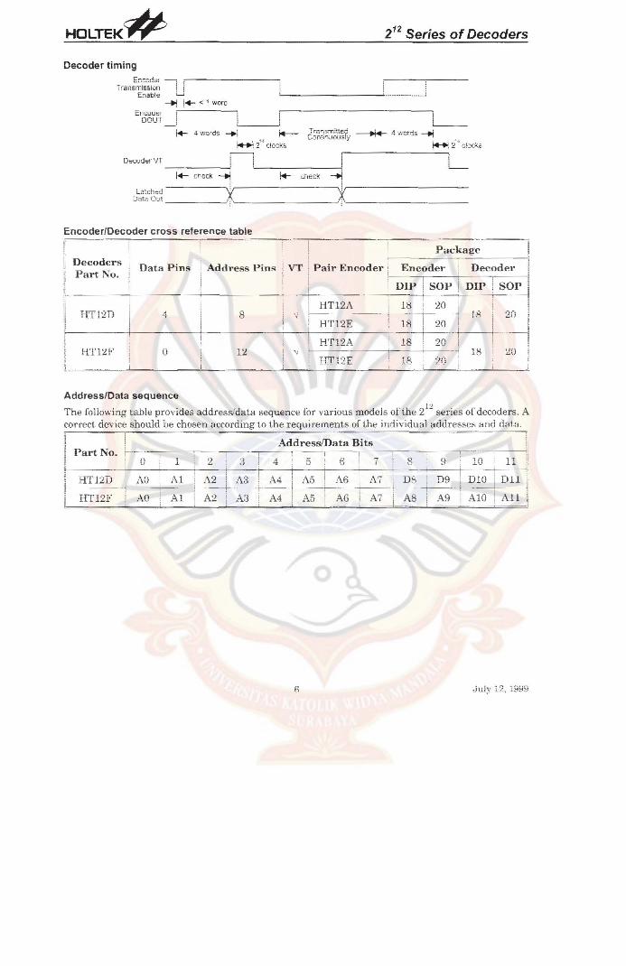
Decoder timing
-, ,~--------------,
T rans r~~:~~ U -t1 i4- < ~ word
Ell(;UU~ 1 I I DOUT _ t L-
-, --~,
D~l.:ud~rVT ---:------'
i+- cl"lecK ~
j4-cloc~:5. '~ '2.·~ c!oc;';s
,..---------------------,
i l __ _ f4-- check -+l
L~~~~~~ __________ -"~r------------------'~ ____________________ ___
Encoder/Decoder cross reference table
Ii Decoders 1 Data Pins Part No.
HTl2D 4
~~T
Address Pins i v~
8 I HT12A_____ , 20 , 'I
-----r--- -1 t8 i 20 il HT12E lR i 20 i i 1i
f---- --+---- - -t------ - -+- --I- - - -- - --;-- - +I-- ----l------i-- -----Il HT12A 18 ' 20 I I "
HT1:Lt' o 1:.1 , 10
L HT 12E , ,-,
LO 20 -'
AddressiData sequence I')
The rollov~ring table provides address/data sequence lor various models of the 2 ~ series of decode rs. A C{ffl't~ct. (kv~ce should be chosen according t.o t.he requirement.s oft-he individu[tl addresses and c.bt.a.
P a rt No.
HT12D
HT12F
Address/Data Bits ~------r--'----'--~
o 1
6
i !
July 12, 19B!:1

HOLTEK#
Oscillator frequency vs suppiy voltage
fosc {Scale}
4.00 1
1-;:'.so ~
! i
r-3<)0 ~
~ 2.50 t·
2J I
i .50 I - -l , 1
( HlOkH z~U]O t- -i l-I
a.50 t-
c.2s l-I
212 Series of Decoders
Rose {D}
2i k.
3Ck
3:3k
39k
4 3k
4it:
~tik
62k
:':;1:11<'
~~~75k -=== :;:{I<
- _ ------- !COk
10 11 12, VDO (V DC l
The recommended oscillator frequency is fOSCD (decoder ) '" 50 fOSCE lHT1:110 encoder) , :;: ~ rOSCE (H'T 12A e ncoder),
July 12, lG!.19

HOLTEK# 212 Series of Decoders
Application Circuits
--"4\ T j----.----, ~! RF!r.~iver Cirr.iJi! f----,
HT12F
Notes: Typical in frared receiver: PIC-12043TfPIC-12043S (KODESIII CORP. ·, or LTM9052 (LITE ON CORP.)
Typical RF receiver: JR-200 (JliWA CORP.) RE-99 (MING MTCROSYSTEM , IT.S .A .. '
s July 12. 199B

212 Series of Decoders
lIoltek Semic-onductor Inc. (Headquarters) No.3 Creat.ion Rd. 11, Science-bascd Industrial Park Hsinchu, Ta1v.'an, RO.C T~ i : 886-3- :;63-199f~
f~x: SS6·::l-563-11R9
Holtek Semiconductor Inc. (Taipei Office} IlY, No.576, Sec.7 Chung Hsiao E. Rd., Taipei. Taiwan, RO.C. Te]: 886-2-2782-963 5 Yax: ;~G-2-2782-!JS:3G
Fax: 886-2-2782-7128 (International sales hotlinel
Ho!tek Semiconductor ( IIOD g Kong) Ltd. lUL711, Tower 2 . Cheung Sha Wan Plaza. 833 Cheung Sha \-Van Rd .. Kowloon. H-:mg Kong Tel: 852-2-'745-8288 Fax: 852-2-742-8657
Hultek Slt!miconductol" (Shani:hai) Ltd. 7th Fi l)I)!', B uilding 2, ~u.889. Y; Shan Road , Shanghai. Chill 8. Tel:021-u'183-GG6G Fax:021 -G~85-n~1::;
Hnlmalc Technology Corp. 4Sfi:-n \Vnnrt Sprine~ Hnu]('v3rn , Suite 41;; , ~'rI :mont, Co'\ R4,:;;i:.1 Ti.:l: 510-~5:!-988U
Fax: C:10-252--BHS;i
COPYrIght·:g 1999 by HOLTEK SE)'llCONDL! CTOR INC. -I The informnl ion appcnring in thi !'l 1 )a1" Sheet. is heliever! t.o \w aCl'urntc nt tht: linlc ofpnhliclllion. How{'w'r, nn ltcK nssnml!s no respollsihility arising: from !h,' US(:or uw ~P('cj"'cat1nn:-: til'scriiu:"t Trw il ppl1cnlintls ment-iollcd herei n iln~
used soic ly fur the puqmse of illu:st r;lliuH aml Hullek lII<.tk(;:-; no wO;:ITi.mty or n :: j.Jl"l'::icaial iuH th<.tL s u ch avplit:alwIl::> will Le :milahle withuu L fu rlher' IlIULiifi calloll, Jlur reeumUll;:! llUS the usc ufiLs pruuud:s fur appJit.::"iLi or1 lhaL llIay j.Jn.:::;cnt a risk to human hfc due to malfunction or othe rwise. Hoitck rcser..-cs the right to alter :ts product::> \~ :tl1out prio!' notificatio:l. For the most. up-to-date information. please visit our web site at. hllp.//www.hoitek.cflm.tw .
9 . j uly u, 1999

:!tures ~!T!pat!b!e 'E!th MCS"~:-51 P!'~d!...!cts , Bytes of In-System Programmable (lSP) Flash Memory - Endurance: 1000 WritelErase Cycles IV to 5.5V Operating Range ill' StCitic 0psiation: U Hz to 33 r.,lMz ~G~-.,!e\:'e! Progr~m Memory L0G~ 8 x 8-bit !nternal RAM Programmable 110 Lines
'0 16-bit Timer/Counters
w-power Id!e and Power-down Modes
errup! Recovery from Power-down Mode Itchdog Timer l'=Ii Data Pointer • •• ___ .c£ '1"""1 __
'w-';v;-:';;; r;;;;:~
st Programm!r'!g Tim'J !xible ISP Programming (Byte and Page Mode)
lory to be reprogrammed tn-system or by a convent!onal nonvolatHa memory prolmer. By combining a versatile 8-bit CPU with in-System Programmable Flash on )nOiithic chip, the Atmei AT89S51 is a powerful microcontrol1er \lvhrch provides a ly-fiexibie and cost-effective SOlution to many embedcled control appHcations.
AT89S51 provIdes the foiiowlng standard features: 4K bytes or Fiash, i 28 byteS of '1,32 UO lines, VVatchdog timer, two data pOinters, two ·16-bit timer/counters, a fiveDr two-level interrupt architecture, a tun duplex serial port, on-chip oSG!tiaro:, and
!riie Mode :?.tor:~. the CPU I,."Jhi!e 8\bw!::g the R_-,ll..~-A; timerjc,o:_:::ter~.; :?,erie! pc:rt end nlot s\i~.tp.m tn r:nntirHlp. tljf1r:tinnincL Thp. PrH,",ip.f-rin\i\i['! mnrlp. ~.rlVP.S tr!p. RA,M c.on--, -.! - -- -- - - - - - - - - "-' - - - - - - - - - - - - - - -
; but freezes the oscH!ator. disabHng all other chip functtons until the next external rupt or hardware reset.
I
~=iil== •..... _-r.1icrocontro!!~r
with 4K Bytes in-System
~
... rogrammabie ~I __ I.- id::J i i
AT89S5i

'1 Configurations
PDiP -----~,
,; ,1:.)S ; ~~'. :" l :~ :1':;;30: r : .~ --i '
i s ("K: P-1 .71 !! R.ST ~ ::
tR :·: ::: : ~;:.:-;J i0 ~.T;(n!p3.~ !'i'i
iT0i :::>3Al i4
:~.~;;~ ;~:~ j ; ~ ,RD~ ;:<3 --: j ~ 7
'.,:T.~;"' ;: ~ if; ':-:;~; ~ l ~ .~
GND j 20
40 :- '.TC .~ :: : ::'0. 0 \ '.::;\;:
3ei POi I:AO,; ,'.1 t f·C:.:.:: ~_"'U/l ~ !-: ! P :~:'": :::':~- '
~~ ! ---.~~ ... ; .~;~ ;
:O:f.. _ " :,o.~ '-.'
'i.7 ~ P2.u 1.':"14)
Z3 i _ P2:.:: { ... ·.13\
:::5 ~ ?2.': :':\:':': ~
;:4 : ' ;:<2 . .3 ~AI f ;
.' .' !-' :.) 1 \A'-l: ~ . : .
'-------
" (
;~_~:.:f" _!: : '~ .... -~ ~
(MlSU) I-' t ,Ii -42
rs·:K) ? ' .7 C; 3 ~~T'-:!
(ii-no :; F ,i . ~ 1 g
! : ~~~; ~L: ~ ~~ :"':" :; P3.5 i! i
c... =- ~ ;.,,: r;-x
~- ':::.
T£\C'D : "..::;::
:~ '"": ' .... ~ ce:;;: ~ ,- ,-
.A.T89S51
i :::{ r- :'(: ..;. ;A::.:.)
':;2 f: p:;_~ fAD!;,:
3. ~ i- ~0.-: ,':"'D€: ; .~::; i tlfl "? ' .. \ij"i"
[" r-cA.-vi·,f.! 2~L:'iC 2: L . .:..:....=i ::l=:O~ 26 r f'SE."J ,(,:, wf.':.: .! ( ;l,~ '; :
:2A tp:< .:.s : . .:.. ~ .; ; ::3 ,', F::.s ~A ~ 3;
::::XD~ p ;:-; :} -1 ~ ~ .~ - -. ~
(TXD: P3. ~ !: 3
('~jT rJ; f"3.:;: _! '4
: '-~ :
::-. .... :~ ~
~ .!
i R5T:1 :
\!~~""D! P'j I) ~ '2
~'.~.~~ (lNT1} ~;:3 q 5
., __ F',}.4a b
;; ! : ?:!:: :i :{WRi P 3.tiQ j
t~~:;:::~~G ;·(1 ;\L 1 ct 11
~.~.,;~~~~~ § ~~ {~e; :""2 n d "! 4
~ . .:..g; ?2.1 1 : 5 fA, ;::!:~;: . ;:a ·:::,
:':".1 j : ?2,3 rl :7 (A12:) P2.4 cj1 !:l;
PDIP
33 ! F0 .: ~Ai):; ?;::; L_ E:~:'~<PP
42 h P: -: (5 '::-:,: 41 p p1 .6 !M!S0:
~~ b ~~ :: (MuS:!
33 b P1.:1
57 bPi .:.: .-:'~! .' ?: :
.15~ P10 34 t "''DD '-::.:1-': , . , •. ,'(.: t.:: 32 P PO.':" (ADO.": 31 b PI-, 1 \AD, 'j .. ~h ~~ ~ . . _ ._. .::;-.;r--:~"-· · .:.. :r,:..:.:.. :
.~ .. ) p P(~3 ~ A [:.~ .l
23 r Fc .-j ~:\L····t:r i7D ;-~-: ::. ;;..:.C:5·;
2£; h P0.5 :::,\L~: 25 p PO 7 (A[f7;
:i:'i i : Ef:"VFP ;;.~. b ALEiP"R0?':
::2PPSEN
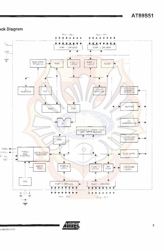
)ck Diagram
GND
• i.)
REGlSTER
POG - po:
rrr.trtr F"i)RT 8 DRj\/ERS
• • 11-': iJ
'f' •
Ace
t Y •
J"\r--l ---, A~U r
i
• '"
•
..... ',. P2 7
rrrTrrrr peRT;: DR1\lERS
• r
PORT 2 L~T:-:!--i
..
...
t
•
~LASH
..
•
4-i
AT89S51
! BUFFER
i-t __ ! ;
i ,,,,CREME,,,! oK r--
! COUNTER ~ L--__ --'
~ DUAL DPT" I. " L--__ ---'
y
\- .! PORT is? PRCCiKA.M
'---r--' ,--.--,1 1'-__ -_-_-_-__ ---' .! *
,------"y- y
PORT DR!\:'ERS
... ... ... ... ... ... ... ... - - - - - - - - - - - - - - - - - - - -:- - -: - - ~ - - ~ - - i- - - ~ - -i- - -: - - - - - - - - - - - - - - - - - - - - - '- - - - - - - - - - - - - - - - - - - - - - - - - - - - ~ - - - - - - - - - -
3
~-iviiCRO-12i03

I Description
c
o
'RVDD
'RGND
to
t1
·t 2
Suppiy voltage (ail packages except 42-PD!P)
Ground (aU packages except 42-PD!P; for 42-PDiP C;~~D connects only the iogic core and lhe ernbedded program memo(y).
Supply voitage for the 42-PD!P which connects only the !oQic corE and the embedded program memory.
Supply voltaqe for the 42-PDIP which connects oniv the 1/0 Pad Drivers. The application board MUST r:onnect both vee ,md PWRVDD tn the board supply voitage
Grouncf for the 42-PDIP v.thich connects oniy the tlO Pad Drivers. P\rVRGND and GND are weakly connected through the common sijicon substrate. but not through any metal link The application board MUST connect both GND and P\VRGND to the board ground.
Port 0 is an 8-bit open drain bi-directionall!O port. /\s an output port. each oin can sink eight TTL inputs. vVhen 1 S Br8 written to port (1 pins, the pins can be used as high-impedance inputs,
Port () eRn also OA configured to OA the muitipiAXAd !ow-orriAr address!nata bus during ar:cesses to external rrogram and oaTa memory. in this moce, PO h8s internai pull-ups.
Port 0 also receives the code bytes during Ffash programrning and outputs the code bytes during prowam verification. External pull-ups are required during program verification.
Port 1 is an 8-bit bi-directiona! !.to port with interna! puli-ups, The Port 1 output buffers can sink!source four TTL inpuis, \f'Jhen 1 s are '.vriUen to Port 1 pins, they are puiled hiqh by the intern:;! pun-ups 8nd can be used as inputs_ As inputs, Port 1 pins that rirF. externaliy hAing pulled low win source currAnt n,;.) because of the intem81 pull-ups
POrl 1 aiso receives the lO\lIj-order address bytes dUr'ing Flash prograrnrning and verification.
P"l .~: .~~~~-
Port 2 is an 8-bl t bj-directional !iO port \"/ith intern,?-! DuH~ups. The Port 2 output buffers can sink!source four TTL inputs. V'fhen is are written to Port 2 pins. they are pulled high by the internal pun·~ups and can be used as inputs. As inputs, Port 2 pins that are 8xternaiiy being puiied !ow wiH source current Otd because of the internai pUii-ups.
Port 2 emits the hiqh-order address byte durinq fetches from external proqram memory and during accesses to externai data memory that use i6-bit addresses (MOVX @ DPTR) in this applic.ation , Port 2 w::;es strong internal puH-ups \-vhen emitting '1 s. During accesses to external data memori that use 8-bit addresses (MOVX @ Ri). Port 2 emits the contents of the P2 Special Function Register.
Port 2 aiso receives the higti-order address bits and some controi sIgnals during Fiash proqramminq and verification.
ATAq~~1 ;, :,.----,.

t3
r
rypp
~L1
~L2
Port 3 ~s an 8-bit bi-directiona! 110 port 'vvith internal puH-ups. The Port 3 output buffers can sink/source four TTL inputs. vVhen 1 s are written to Port 3 pins. they are puHed high by the internal pu!l-ups and can be used as inputs. As inputs. Port 3 pins that are externa!!y being puiied low wiii source current (I,; ) because of the pun-ups.
Port .3 receives some control signais for Flash programming and verification
Port 3 also serves the functions of various special features of the ATS9S51. as shown in the foiiowmQ tabie.
) -~,
j-- ----l i r-::j,f
Reset input .A high on this pin for h ... .ro machine cy(:ies v,/ni[e the oscillator is rl)nning resets the dev~ce. This pin drives High for 98 oscii!ator periods after the vVatchdog times out. The D!SRTO bit in SFR AUXR (address 8EH) can be used to disable this feature. in the default state of bit DISRTO. the RESET HiGH out feature is enabled.
Address Latch Enable (ALE) is an output pulse for ~8tc-h;ng the !O't::' byte of the address dUf!ng accesses to external memory_ This pin is a) so the prograrn pulse input (PRO G) during Flash programming.
in normal operation, ALE is emitted at a constant rat,e of 1/6 the oSG!Hator frequency and may be used for external timing or clocking purposes. Note, however, that one ALE puise is skipped during each access to externai data memory.
If desired, ALE operation can be disabled by setlin<:j bit 0 of SFR location 8EI-I. With the bit set, ALE is activA only during a MOVX or MOVe instruction_ Other-vise, the pin is weakly puiied high, Setting the .AL E-disabie bit has no effect if the microcontro!!er is i!'1 eX.terna! execution mode.
PrOQfalTl Store Enabfe (PSEN) is the :ead strobe to Bxternal pfograrn memory
\:'Vhen the AT89S51 lS exec~tinq code from exterr:a~ proqram memory, PSEN is activatf:d twice each machine cycie; except that two PSEN activations are skipped durinQ each access to 6xtern81 data mRmory
code from external program memory locations starting at OOOOH up to FFFFH. Note, however, that jf lock bit 1 is programmed. E!-\ win be interna!1y latched on reset.
EA should be strapped to V:-.:-: fO!"internal program executions.
This pin aiso receives the 12-volt programm ng enable \loltage (V'F?) during Fiash programming.
~nput to the invening osc!!lator arnp!ifier and !nput to the internal dock operaUng circuit.
Outout from the invertlng oscillator ampiifier
5

ecia! ..... .=."':_= iivi.iUli
gisters
.fl. map of the on-chip rne:TIory 8cea caHed the Special FunctiGn Register (SFR.l space is sr~Ol:",..T! in Table 1 .
;-iote I;-iot not tl;; of the tJddresses .]1 e OCCuPiCU. ,:;nd unoccupied .Jdd(es8C:s n;;Jy not be ienpie mented en the chip. Re3d 2GCessc:s to th::-se Dd:jfes~:~:s '-l..';;; ~n g:::n:~r8! f"Gturn rundofr: dZ;t8. and ~".;rite accesses ~~:;'! have an indeterminate effect.
e 1, AT89S51 SFR Map and Reset Values
FF,H :.)f-FH
F:':H
-"-':-j
88H
BOH
AOrl
onOO(1(100 ---- ----------+--
:'\.cc C:uOOOQOQ
DC:C:OOOOD
P3
00000000
11 i 1 "1 11 "'1
:-CON 00000000
pn
1--: '11111
SGLlF
T:'..'lC:D oooonooo
SP 00000-lil
XXXXXXX:: -~--- --- -----+---
TLO 00000000
00000000
AT89S51
onoooonn
DPOH 00000000
THO ooonoooo
00000000
TH1
ooonoooo D~'~H
OOOC)OOOO
:o:xxxxxx
X)<XOOx.x.O
PC-ON OXXXOOOO
~IF7H
'1~- :- n
:::;:-:-:
'JCFH
JC7H
OBFH
0B7H
OAFH
DA7H
BFri
j-MiCRO-i 2/03
AT89S51
User sofh-vare sholJld nOT write 15 to these uniistAd iocahnns; sinCE they may tip: used in Tut!Jre Drc:duc:t~, to invoke ne\'v features In that case, the reset or inactive va\ues of the neVi bits wiii always be [;
jnterrupt Registers: The lndiv!Qual interrupt enabie bas are in the iE re~ister_ T\lIJO priOrities can be set for each of the five tnterrupt sources in the IP reqtster
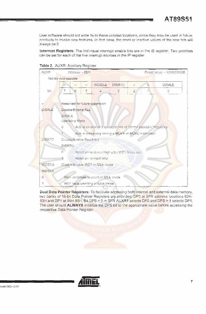
Table 2. AUXR: Auxiliary Register
,t:..UXR
Not Bit .A.ddr8ssabie
VVDlDLE DiSRTC DiSfo.LE
6 2
Reserved for future expansion
DiSALE Disable/Enable .A.LE
D!S.ALE
t,-,.- f.·.~ .• -•.•. -.. ---, "- J
Dl2.R.TO
\,VDiDLE Disabie/Enabie VVDT in iDU:. !l,Qde
Dual Data Pointer Registers: To facilitate accessing both internal and external data memory. two banks of 16-bit Data Pointer Registers are provjded: DPO at SFR. address ioc8tions 82H-8:3H and DP1 at 84H-85H. Bit DPS ~ 0 in SFR AUXR1 selects DPO and DPS ~ 1 seiects DP1. The user should ALWAYS initiaiize the DPS bit to the appropriate value before accessing the respective Data Pointer Register.
7

mQry
gram Memory
a Memory
tchdog ner
abied WIth
set-out)
ing the WDT
Power Off Flag: The Power Cff Fjag (POF) is located at bit 4 (PCCNA) in the peON SFR. POF is set to ;;1" during power up. it can be set and rest under softwarE' control and is not affected by (eSBL
Table 3. AUXR1: Auxlilary Reqlsierl
ur-.-'
Bit 7 ..
DPS
t\.~CS-51 devices have a separate address space fcr PfDgran-, and DE\tE! ;,/lerncfy _ Up to 64K bytes each of external Program and Data Memory can be addressed.
if the EA pin is connected to GND, ail program fetches are directed to external memory.
On the .A.T S9S51; if EA. lS connected to \/ c-c-; pro~v?m fetches tD addresses GOOOH throu~h FFFH are directed to internai memory ;:znd fetches ta addresses -1000H through fTTr:H Rrp. directed to extern?! memory
TheAT89SS'1 impiements '128 bytes of orH~hfp RAM The 128 bytes are accessible via dfrect and indirect addressing rnodes. Stack operations are exarTipies of indirect addressing, so the 128 bytes of data RJ\M are avaiiab!e as stack space.
The VVDT is intended as a recovery method ::1 sltuat:ons where the CPU may be suo!er:ted to softwRre LlpseTs. The VVDT consists of a 14-bft counter <=ind the Vv'atchdog Timer Reset {'.tJDTRST) SFR . The \NDT !S defaulted to disable from exiting reset. To enable the \/\/DT, a user must write CriEri and OEH--i in sequence to the \fVDTRST register (SFR iocation OA6H) Vyhen the VVDT is enabied, ~t :.;viii inCrement every machine Gyeie :.-vhiie the oscWator is running ; ne \;~U; timeOut peroc:j ,5 aependent on the e;;.tern3.; C,OCr, frequency. ; nerf:; 15 no -"':',/3.y to 015-.:;!::!8 t!--·~ \/'.JDT -?xcept th:c:u:~h :e5e~ (either h8rd."vare r8E·et or l.:VC:T O'.f8rfiov'''! reset). \Vhen ;"'\IDT overt!ol.:vs. it ',."!~H drive ::!n output RESET H!GH pulse at the RST p;n
Tn An;::;h!e the \'/\'/DT, R u;:;er must \./ljrltP. 01 EH ;:lnri DE'l H in ;:;ellllp.nr:p. tn thA \/VDTRST n;gister
(SFR location OA6H) . \!Vhen the VVDT is enabled; the user needs to serv'ice it by writing 01 EH and OE 1 H to \/\iDTRST to avoid a \:'\lDT overfio\."V, The 14-bit counter overflows when it reaches 16383 (3FFFH), and this v"di~ reset the device. \Vhen the VVDT is enabied, it wiH increment every machine cyde while the os-ciliatof is funning. This means the user must reset the V\!DT at least every 16383 !l18Chine cycles. To reset the VifDT the user Inust write 01EH and OE1H to Vv'DTRST. 'vVDTRST is a write-only register. The \f.jDT counter cannot be read or wr;tten. 'vVhen 'lV-DT ovetfi0v.iS, it 'l1i!l Qenerate an output RESET pulse at the RST pin. The RESET pulse duraUon is 98xTOSC, where TOSC = 1/FOSC. To make the best use of the \lVDT, it shouid be serv!ced In those sections oi code lhat wiii periodicany be executed wilhin lhe Lime required to preve!'lt a "\lDT reset.
'~.>~n • ".-".-. _, .e:....,.._ .• '--_ ... "._ ..•. -

>T During
RT
ner 0 and 1
errupts
AT89S51
!n Power-dovvrl mode the osciilator stQPS~ which me2ns the '1yDT aiso stops. \Nhile in Povlt'erdown mode, the USer does not need to serv:ce the \lVDT. There are two rnethods of exiting Power-down mode: by a hardvvare reset or V18 a levei~actjvated external interrupt, \;vhich IS enabled pnor to entering Power-down mode. When Power-down IS eXited with hardware reset, SerV!Cfnq the \NDT should occur as 1! normally does whenever the ,A, T89S51 is reset. Exitinq Power-down with an interrupt is signific::mt!y different_ The interrupt is held iaw fong enough for the osciilator to stahilizA- \/VhAn the interrupt is hrought high, the interrupt is serviced. To prevent the \/"JOT from resetting the device whHe the interrupt pin is held iow. the V\fOT is not started until the interrupt is put!ed high. It is sugges1ed thai ihe vVDT be reset during the inter(UDt service for the interrupt used to exit Power-down mode
To en.sure that the \11101 does not overflo\'1/ within a rev,; states of exitinQ Povl,ler-down, it is best to reset the \,IVDT just before enterinq Power-dO'.."Jn mode.
Before gOlng into the [DLE mode. the VVDtDLE bit to SFR AUXR \50 used to deterniine whether lhe V\fDT continues to count if enabled. The \NOT keeps counting during IDLE {\ND!DLE bit = O} as lhe defau!l state. To prevent the WDT frorn resetting the AT89S51 whiie in !DLE mode. the user should aiways set up a timer that vviH perioDicaHy exit IDLE, service the \NDT, and reenter IDLE rYlOcie.
Vvith 'vilDiDLE bit enabled. the V..fDT win stop to count in lDLE mode Bnd resurnes the count upon exit from iDLE,
Th~ UA,R,T !n the AT89::;f)1 or:~f;3tes the s:~me w:~y as the Up· .. RT in thR AT89C51 Fnr tUrf!!Rf
information on the UART operation, refer to the Atmel Web slte (http://www.atm€Lcorn). ~rorn the home page. se!ect :tproduGts", then HMil::rocontfoliers'!, then "8051-.Architecture'~. then "Documentation!!. and "Other Docurnents". Open the AdobeC'C:' Acrobat:;;:' nie "/\'T89 Series Hard
ware Description".
TimAr n Rnr1 Tim?f 1 jn tnp. .A. TR~S~'l nf)Ar;:;tp. rn? Sr:lmp. '-"J?JY RS Timer [1 .~H:rl TimA: '1 tn thE: AT89C51 For furthe.r information on tr,8 timers' CJperation. refer to the Atme! Viet: site (httoJ!www.atrn.e!..com).Fromthehomepage.seiect "Products", then "i\~icfocontro\lefs", then "8051-Architecture", then "Documentation", and "Other Docunlents". Open the Adobe Acrobat fiie "AT89 Series Hardware Description".
The ATB9S51 has a total of flve interrupt vectors: hvo externat lnterrupts (!r-.JTO and !NT1 L t\~'Vo timer interrupts {Timers 0 and 1}, and the seriai port interrupt. These !nterrupts are aH shown in FigurF: 1
Each of these interrupl sources can be individuaily enabled or disabled by selling o! dearing a bit in Special Function Register IE. IE also contains a Q!oba! disable biL E.A,. wh!ch disables aH !nterrupts at once.
Note that Table 4 shows that bit positions !E.f3 and !E.5 are unirnp!ernented. User softvv'are should not ilirite 1 s to these bit pos~tions, since they rnay be used in future ATBS products .
The TimAr 0 ann Timer '1 flags, TFO and Tr1, are SAt at S5P2 of thA cycle in which thp. timers
overflow, The va rues are then polled by the circuitry in the next cycle
9
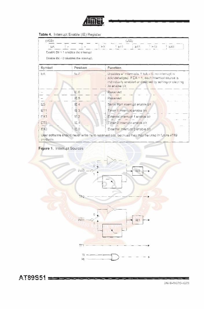
Table 4.
ET1
EX1
[TO
EXO
interrupt Enabie (IE) Register
H:: . .7
lEA
lE_3
iE_2
C,", ; c_XU
:nd:'-!idu~t!y t"::2bied Qr :jis2u\ed L~y se1! :~-:n nr" c-!e~; :ng its enable biL
User sorr.Nare should never write is to reserved bits because they may be used in future AT89 ~rod:_j{:,;ts.
Figure i. int8frUpt Sources
~ :-~L-J~
-. --- ---- -- -- -- "-- ---.
~ :t-iNT 1 ---(-" ...
. A.T89S51
r--1 :~;.j !El i-__. , L-J
i----.
--j

cillator aracteristks
~ Mode
wer-down de
XT.A.! 1 ~nri XTA! / ?:~ the lnf):lt 2nd Gt.!tpU!, :p.sper:t[;!F.ly, CiT Rn in'.JF.:iing ?mp!iT!R!" tr-:2t r:8!: hp.
r:onfigured for lise as :,n on-chip Q5diiator, ,~s snO'-Jvn in FigurA 2_ ~ither a qU::lrt7 crystF.lI or ceramic resonator may be used, To drive the device from an external c!ock source, XTAL2 shouid be left unconnected whHe XTAL 1 is dr!ven, as shown in FiDure 3; There are no reauirements on the duty cycle of the external clock signa!, since the input to the internal docking Glrcuitry is through a div!de-by-two fllp-f!op. but minirnurn and m3xirrrum vOllage high and low tirne specifications rnust be obser~/ed.
Figure 2. Osci!iator Connections
• :!
,-... t, l ',_ •• ~ ::in pF _L 10 rJ~ for CrVS[8!~
40 of ± i Q pF for Ceramic Resonators
Figure 3. Extern8! Clock Drive Conf~guration
S:G~iAl.
In idle mode. the CPU puts !tS8!T to sleep whHe aH the on-ch!p penpherais fema!n actiVe. The mode is invoked by soft\,vare. The content of the on-chip RAM and ali the special function reg
isters remain unchanqed durinQ this mode. The idie mode can be terminated by any enab!ed intp.rrupt or by a hnrriware reset.
Note that when idie n10de is terrninated by a hardware reset the device norrnaHy resumes prol;r8.r(t executtorl -[roen where it left orL up La 1v'-:,0 rrlfichlne c;'{c\es before the internal reset 81gorithrn takes cont(oL On-chip hardware inhlbits access Lo internai RAM in this event, but access to the port pins !s not inbibited. To eliminate the possiblilty of an unexpected write to a port pin v'-Ihen idle rnode is term!flated by a reset, the instruction fo
)gram mnrv Lock -----,;
}orammino -.- ------------
~ Flash-raiiel j'vlode
Table 5. Status of Externai Pins During Ie!€' a.nd Power-down Modes
ALE PORTO
idle UEHa Data
lQ:'2- Externa~ FiOE!:
Pavlfer-aow:! Q o Data Data
Exte:na~
n~o"":,,,~ :-~:'.:.:..
Data
,ll,ddress
Data
DatB
Data
Data
rhe .A.T89S51 has three iock bits tha! can be left unproQrammed (U} or can be proQrammed
(P) to ontain the additional features listed in the fol1owlng table
_ ....... , ..... - ...... , " .. ;
i aLiie u. LOCK DiI r--TOi:eCnOn i\/iOOe5
Program Lock Bit~
LB1 LB" LB3 Protection Tyr)e
, , ; - -
-------------------i 2 , , L , f~'C(Bi-i-:;C:: i-::O~y8!-:: :-;-:8!-;-:C::-Y-
R •• - ••••• ____ •• ___ •.••• _ ••• _.,. __
!~'a_n! 1 __ , u L'cil! :)l, ;\!~n!.~ ~):_"" ,- :u PU : : j.
are d~sab~ed fro::,: fetch\ng cc-de bytes T:O:T: ::-:te:::3i :::0;:; : : . ....:: y.
3 p p S3f::e 3S :::cde 2. but verifj is alsc disabled
V·.Jhen jock bit 1 is program!ned. the 10gic level at the EA. p1n !S sanlpled and latched during reset. !f ihe deVice IS powered up Witt-lout a reset, the iatch initializes to a random vaiue and hOlds lIlat value untii reset is activated. The iatched value of EA (nust agree with the current logic levei at that pin In order for the deVice to function properly.
The AT89S51 is sh;pped ,:vith the en-chip F!8Sh memQry array ready to be pfogfarnn1ed. The progranlming interface needs a high-VOltage (12-vo!t) program enable signa! and IS compatible with conventional third-party Flash or EPROM p(ogranlnlers.
Programming Algorithm: Before programming the AT89S51, the address, data, and controi signais should be set up according to the Fiash Programming r,Aodes table (Table 7) and Fi~ures 4 and 5. To proQram the AT89S51, take the foliowinQ steps:
1. input the destred rnenio;,y location on the address lines.
2. input the appropriate data byte on the data lines.
3. .Activate the correct combination of control signalS.
4 Raise EA/V pp to 12V
5. Pulse AL.EiPROG onr.e to nrogi?m ? byte in the F!ash array or the lor.k hit~. The hyte-
wr~te cycle is self-timed and typicaHy takes no [Tore than 50 iJs. Repeat steps 1 through 5, changing the address and data for the entre array or untii the 6nci of the object file is reached.
Data flailing: The .A,T89S51 features Gata PO!!lnR to indicate the end ot a byte write cycle. DurinQ a write cycie, an attempted read of the jast byte v/ritten wiii resuit in the compiement oi the written data on PO.7, Once the write cycle has been compietea, true data is valid on all outputs, and the next cycle may begin. Data Polling may begin any time after a write cycle has been initiated.

19ramming ! Flash-
'la! grammin9 orithm
AT89S51
Ready/Busy: The progress of hyte programming can also hp. monitored hy the RDY/BSY output signal. P3.0 is puHed !ow after ALE goes h!gh during programm~ng to indicate BUSY. P3.0 is pulled high aga!n when programming is done to indicate READY.
Program Verify: If lock bits L81 and LB2 have not been pragramrrled. the progran"lrned code data can be read back via the address and data iines fOr verification. The status of the individual lock bits can be verified directly by reading them back.
Reading the Signature Bytes: The signature bytes are read by the same procedure as a normal verification of locations OOOH. 100H. and 200H. except that P3.6 and P3.7 must be pulied to a logic iow. The values r"ettlrned arB as foiiows.
{OOQH) - 1 EH !ndicates manufactured by A.tme\ (100H) - 51H indicates AT89S51 (200H) = OSH
Chip Erase: in the parai!ei progr.:}mming mode, R chip erase operat~on is initiated by using the proper combination of control signais and by puising .ALElPROG ~ow for a duration of 200 ns -500 ns.
in the seriai proqratnming rnode: a chip erase operat!on is initiated bV issuIng the Chip Erase instruction. in this mode, chip erase is seif-tfmed and takes about 500 ms.
During chip erase, a serial read from any address location will return OOH at the data output.
The Cc:!ie mem::1rv r;!'TRV ~p.n he nrngrRmm8d tl~.~nq the serj~l !SP interf?~p. \ ..... Jhile RST !s Dul1P.r1 to Vee ThF. SP.iiFii interrace consists of pins St:K; ~\{10SI (input) and MISO (output). AftAr RST is set high, the Programming Enable instructiCin needs to be executed first before other operations can be executed , Before 8_ reprogramming sequence can occur, a Ch~p Erase operation is required.
The Chip Erase operation turns the content of every memorv iocar[on in the Code BrrBY into FFH.
Eithei" an external systern dock can be supplied at pin XTAL 1 or a crystai needs to be connected across pins XT,A,L 1 and XTAL2. The rna.:r.linUIT! serial doc~, (SCK) fi8quency should be less than 1/16 of the crystal frequency. 'vVith a 33 MHz osdHalor ciock~ the rnaximunl SCK rrequerlcy is 2 i\.~Hz.
i' Q prof1!'".8rr! and verity fhe .-u.f89SS-1 ;n th~ s~r!ai prQqrp~rr-mirq::~ mode the foilo'.:v!nq sequence
is recommended :
1. Power-up sequence:
Apply pCiwer betY~.JE;en vee and GND plns.
SeT RST pin to "H::.
if a crystal IS not connected across pins XTAL 1 and XTAL2. apply a 3 MHz to 33 MHz ciock to XTAL 1 p~n and wait for at ieast i 0 miHiseconds.
2. Enable serial programming by sending the Pro:;iramming Enable serial instruction to pin MOSIIP1.5. The frequency of the sr;~ft ClOCk. supplied at pin SCK/Pl 7 needs to be 18SS than the CPU dock at XTt-\L 1 divided by 16.
3 Tr!e Code array is programmed one byte at a tirr!8 in e[ther the Byte 0: Page mode The v.,:rite cycle is self-timed and ty'picaHy takes less than 0.5 ms at 5V.
4 Any mp.mory ioeation can be verif~Ar! by using thR Read instri.lr:tion that rATurns the r.onTRnt 8T the SAl Acted 8rk-lress at serial output M1SOfP1_D
5. At the end of a proqramft'!lnQ session, RST car: be set low to commence normal device operation.
13

ial gramming :ruction Set
>gramming
raiiei IVlode
Power-off sequp.nC:F! (if nF!AriRO)·
Set XTAL 1 lo "L· (if a cryslCil is not used).
Set RST to "L".
Turn Vee po\.ver off.
Data Polling: The Data Po!!inq feature is also avai[abie in the serial mode. in this made; durinQ a write cycie an attempted read of the iast byte whtten wil! result in the complement of the !v1SB of the sArin! output byte on MiSO
The instruction Set for Seriai Programming foiiows a 4-byte protocol and is shown !n Table 8
Every cc.:de byte [n the F!ash array can be programmed by us[ng the appropriate c:Jmbin2tic~n of control signals. The ~vrite operation cycle is s6!f-iimed and once initialed. will automatica!iy L!rYJe itself to cornpletion.
r.."iost ::--:-3Jo; '.,.~,.'::!r!:j'"v~de Pf:J9:8m::--: '"19 v8ndc:r~. c;Hc.r 'l'!orld'.,.A/i:jc. ~.UpP:Jft for the /\t!:"!e; /~.T89 rniCfGCentreHer serjes. P!~'£"rse GGntac:t yeur jOGa~ prC:;l:ornrning vendor f:::r the appropriate soft-ware revision.
e 7. Flash Progfafnrn~ng Modes
ALE! FA! Pi} 7 -0 P2.3-:J
R.ST PROG P3,; AddlHSS
H
A7-0
)(
H x ---~'--
H H x
H
H H DDH i .~ _ __ ~ _ _ ~ __ ~ _ _ ~ _ ______ ~_~ ___ ' _ _ L-_ _ _ ~ ___ '~
S Each PROG Guise is 200 ns - 500 ns for ChID Erase , L. Each PROG pUlse is 200 ns - 500 ns for \lVrite Code Data. :3 Eaen PROG Dulse is 200 ns - 500 r-:S for \Vnte LOCK B:ts , 4 RDYf8SY signai is output on P3.0 during programming. 5 X.= :jc:n't c:are.
-'~"''''D ~J'."''''.-.. "-,,",'-"''-._OU •• •.••• __

3-r,·~lCRO-i 2/03
Figure 4. Programming the Flash (vip-mary (Parailei !\.~orie"
:\0 _ :\"7 .~
aaOQH.'FFFH ! ;OJ
: ---- ~: '3EE. ~ 1...:',3 ~
P=<OG RM.,u,;\iN Gl --i ... _--_ . ..!
!
P2.:
Figure 5. Verifying tn? Fin~h Mp.mory (Paranel iviOrlA)
PGM
~--- "
,~,1cI3SS"i
,~.:JUH ~o -_".: -..f P'1.iJ-P~- . ? '-..:~~j :.::.~"~ :.;.:.:.::.
L~ __ ~~~-i P20
SEC FL';-j i! - ~ :~! Mt-IOE~ =A.EsLE' ~ P3 a
=
•
AlmEl "
_--+\ v:' ,
P5EN
AT89S51
'i 5

Ish Proarammina and Verification Characteristics (Parallel Mode\ - - ~ ~ - - - - - - - - - - - - . - ':. - - - - - :
: 2(r'C to 30~C , Vee = 4. 5 to 5.5V
11.5 12.5
P, oyra;;;;:;;:;~ S:.JppJy Current 10
\:'.::c Suppiy CLi rrer: t 30
C:3cijiator Frequer:cy - --- -
;\X Address Hold After P-ROG
Data Setup to PROG Low .----;-----~___i
.:1,0 . - -Cl.C! _____ _____ ~.
S L VPF Setup to P"ROG Low
)\.. ,u...uure:::;s tQ Data Va!!d '-'---- - --+-
E N~A;8LE Low to Data Vai,d
Data Float .A.fter ENABLE
Byte \:Vntt! Cycle 11r::e ----'--"'---_.
ire 6. Flash Programniing and Verification \Naveforms - ParaDe; Mode
P1.0 P'!.7
P2.0 P2 .3
iO
10
, ." :.'~
50
PORT 0 -------+--<t._---,_.:;D_A_:rA_; "'N_-,--~))-: --+--------« DATA OUT ~>-----~ :_ :; . ~I tD'·:'GL. t,'3!-!DY ~
ALE/PROG
P'') 7
P3.0 {RDY!8SY}
\:~··~·;:;i. :-. ---~ :-. ---I ;
4---- :. lC~Q"': ~
____ -J/1-----------~----
4-,
tsr.EL -1 r-' -------------------------~---\. BUSY )1
f+--- t~~.: :~ ---+l
i -:--
READY
, -,.,.,-- ---.

AT89S51
re 7 _ ~iash rv1emory Serial Downloading
\:.:c:
ATB9S51
iNSTRJCTiON II>j P15/MOS:
P1"6lM!SO
---~ F-: 1 :~C::-\
• RST !"III! 1
• GND !
sh Proarammina and Verification Waveforms - Serial Mod~ - . - . . . . . .
re 8. Ser~8j Programrning Waveforms
PLS (Mas'")
P1 7 (SCK) !l rl II r-! Il n rl r--l
___ ---'i ~ ~ L-j ~ L-J i ___ i ~ ,1 ____ _
6 " 3
17

e 8. Serif!! Programrn!ng instruction Set
,
! ::=t:L:d~c:::
F orm:l!
~~ .'~ .-. ~ .... y , .....
xxxx xxxx xxx~-( xxxx
.......... t ..... , ~' '''.: .. " .. "
En;.o!e Se: 3! P;oq:3n::;;~~g
v\,'h ii e RS T is :::g~ ,
rl.l!lSO) : --~--~-------.-.-,--------- ~----------'------~--~--~------.. --. . -.--.-- -
EJQ:·: :.::-::-:;.: :-::-::.::--: ? ""-?\; '. '" '. ' .~
,~ .. ..... o::S~d
~ .... -~-!---.. ----~j------.-----~ ; ; : ~; xxxx xxxx
:::,c Loc.k B~ts i 0010 OiOO :<x:<x xxxx ! :'OO{X XXXX Read b:3Ck G:jffer: f Sfstus of
Ule iuuic. U:L~ (8 progra:":'lfr:eu
......... --.... - ... ---~ ..... -~-,--------~------j
inDn R:=:Aci Signature By18 .
3d Program Memory He f"'10ce)
GOll GGOO xxxx '- 0':;;'00 -C'C4:4: ~.:. -;;;.
i:3yte U Kead data t:-om Program :-:-:er:-::-::-,. ~ :-: :~:~ Pr.fjf.: Mi)(h~
(2':,6 L:y:.,=~ }
1.
0101 OGOO xxxx
81 - I) 82 - 1 -1v1oCie 2, iQCk Oit 1 activated B1 1, 82 ~ 0 .. ::f\.1ode 3. iock bit 2 activated bi - "1 , 82 -:: 1 --tviode 4. ~0ck nit 3 8GtiV<?!t8ci
8yte [:
EACh or rhe lock hit ':lodes need to be RctivCited sequentiaiiy be
tore Mode 4 can be executeu'.
After Reset signal is high. SCK should be low for at !east 64 system cioCks jefore it goes higrl to ciock in the enabie data bytes . No pulsino of RA~et signa! is necessary. SCK s!-;o u~d be no f~~t8r than 1J1G of the syster.-: r:inr.k ~t XTAL 1
r-::.'r Paye Re;;;u/'vV n te. U"ie uala a1ways st8rt~ (ru;;; ;"lyle 0 i\..: 255. AHer n,e ct)tr;;!!t:H!U uyt~ 8nd upper atiure::;s tJyle are latched; each byte thereafter is tieated as data Lintl a li 256 bytes are sh~fted ~:;/Gut. The:: the next ~ nstruction wi1l be ready to be (i(;c0d(;;J.
ATRQ~~1 ~ ... ____ :I

AT89S51 ~rial Programming Characteristics
gure 9. Seda! P rog rammin~ Timin~
rv10S!
SCK
fv1!SC
hie 9. Serla; PruQlarnrnillQ Characteristics, T A = -40" C to 85'0 C, V,:, ~, = 4,0 - 5,5V (Uniess OtMrvvise Notedj
Typ
1 Osci;i;:;!tof Freq!..:snc',l .~ ~.-... -.,.---------..
.1Q
.. _-+-- - -!(~L('L -----~
. _._------ -!--- --------1--
------+---
U;-;lts 1 --<
MHz -------!
r:s
::5
:-:5
·----1
. j , i
. ------!
19

solute Maximum Ratings'" ....... -55 'C to'" i25'C
-~.~.'""IT :t ... ::. " ...... 1 'V1... .
.-.~: to ..;. I .D\:"
.. o.6v
Qutp~t Curren{ .
Characteristics
va!ues shown in this t3bie J:re valid for T . .; - -40::C to 8;)'-'C c..nd Vcc
Conditio::
~~;'-.::5:;~~ UQyvr:0 ~i;U:ii..: f;::;Luu Wi iUl;;;i O>Ai.; ::;u;ui<i ~ .... ~p.; :·:i:n;;::: R;;t~:;gs" :::2}' C:2~£e pe::::2::6r:t d?m-
!:Ige :.0 tt:e liev:ct.'. i h!s 15 a ':itre~':l :Bt!f!'J on iy and fu::ct\on,s\ ope!"?t:.on of the '::levice at these or anv oti'lI::'" CO~"'!d:t:Or'!S bey-oii(! thOS- 8 !r.Ci!Cat8(j :n tr"'le
cO!:0it(ons for extended periods may affect d8V:;':;C ;C\;8u; :ty.
4.0V to 5.5\i, unless othervvise noted.
U!"!!ts
1r:pur Low Voltage (E . .t:..i ·0.5 Q.2 \/:~:~·O.3 --------------------------~--------+---~--~----~
v
lnput H:gh Vo;tage
Guto:A l..JJ-::'"' \/.:':;£Ui:!::'~· : ;oo:! Q, .A.LE, PSCN)
.~ .
Uulpul Hil.J~: Vo\tage (Ports '1,,::,,1; ,L\LE, PSEr{:
(Ports ~ ,2,3) - ---
(XTAL1. RSi}
P(: ,- __ , \fcc
;i'-~ = 2"..1. = ::;:;: , -II""'IC' ..:.. : . ..; Ie
!::.p::: L~2."j.~,--~gf': : .::: ::;nr {PD':: D . .t-.~ i).A !.:: -( ':,::; .. ...-: :" ;_::~ -~-
Test Freq ~ 'j MHz, T~ ~ 2S=C
C.7 \icc
2 .4
0.75 \.le.c.
[) q \.: --2.4
0.75 V~, -=-~-------+-
o.t: '.,"
5(,;
U~-: d~: :::::=:~rj,:-, ~r.::re (:-: tl~-:~~:;?:::S ~ f:i-:r) :-.:-::":(j ~ fc-,:-;s , ::)~ :-r:::.::.: h8 F:~·re:::.? ji y ;;:-:iif:d .":~. fc: ~ c-i~~.;~"
~1! 2X; ' "V .. ··-·· L:,~ :::~er per'. f..':" -'!:~ 'n.n. MnX\murr! L per 8-b\t porr: Port U. LC mA ~orts 1. 2, 3: 15 rnA Maximur!"! totc! l:)L for ali Otitput pi;-:s: 7'j f!"1'u'
- -,-, ,_ .. ---t
0.45
---~i--~ -
6.5
v \!
pF
rr':p.,
---i ,
i ; lO! axceeds UH~ test conuflliXi. \!':"1L ;';'""1s)" exceed the re1aleC spec! t;cation. P;ns Clre not guari::l:--:teed to S!!iK ci..irrent greater than the iisted test condition E. .
.l\T89S51

Characteristics ~r operati!1Q (:Qndihons, iot=!n capac!t:.:;r:ce for Port D, .~LEfPROG , 2nd PSE!'·! uts = 80 pF.
terna! Program and Data Memory Characteristics 12 MHz. O:sciiiaior
AT89S51
'", Of) pF: load r.~pacitan(:f:! fo r a !! other
vCtfiaiJie vsciiiaior .-- - ---,--- -----
nboJ Parameter M'n Max Min Max Units
OSSl~\atof Frequency 33 ivlHz
.. :;du:css Val;d tv ALE Lo'.:v 43
x ,ll.ddress Hold After ,~LE Low 48 tCl Ci.. -25
ALE Low to Va!id Instruction in 233
t- " -2:-
PSEN LO'N to Valid Instruction In 145 3tCLC[ -60 ns
!nput instruct!oq Ho!d After PSEN o o input ~:;~~::..:ctG;; flost ,:1.fter p~;:::~~ ns
--------~------,-.~..: (,;". -u ___ ~--
Address to Valid instrvct:cr: i;-: 312 tiS
PSEN Lev,,! to Address Fioat '10
4QQ
VVR Puise VVidth ::5 t\:;LC-: - j DO - - - .. ,------------ --i------i---- -----i-----"::::..::......---+-----..;..----;
RD Low to "/ajjd Data In
Data Ho!d .u.fter RD ::..c------t-
:\1 Address to Va !!C~ Data in
ALE Lc·'-"! to RD or WR Low
-- --,.t:..ddre-ss to RD or l·;'VR Lo'.,:"'!
Data Vaild to VVR Transition
L Data Varid to 'vYR H!gh
P.D or iNR H\gh to ALE H\gh
- MiCRO-i 2/0,}
Q
200
2Q3
23
433
33
43
AIIIIIiL ----_ ..
252
o 97
517
585
sOO
7tC:t cl-130
123
n5
9t(:lGL- '!65 ns ---t---
34.: ~--:: +50 ns
ns
_c
ns
·-1 I
. j
21
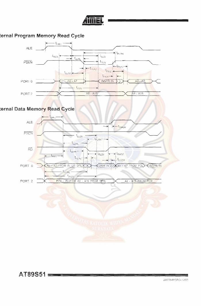
term~! Program Memory Read Cycle
j+---- t. Hi i ~
.ALE __ Y '\. r-~----:. ,;:::=========:-\ f.:=.j p~
l.';"\ilL ;'i·~--~·';i~·---+-----·i' \LF. ~ ti....i....? :'" :.--
"'---_ / 'r~=====J·i~t_c_·u_v ___ ~ "'-) ;4--tpy,.o: .... --+!
--f!oj f+- t; ''-~.z Cl...L:1.X :f<,f----,.,(
: I ~!'.r L){~
_____ ~)--K~_-'-p..:;.;J:..· --,-.~:.:7 __ ~:t-: ----i(~ iNSTK iN PORI 0
t. ..... .! -------~~------------~A~.e~. -- ~A~'~,:~.-----------------'"'r--~~.~~~---~~' 7' ~5------------------J/T' /-~~---~----------
ternal Data Memorv Read Cvcie .; .:
ALE
:-:--- -- - - ---::
~ ttLA,X ------i '1'~--+---~/' .:"--· . i :.qi..D'.! ~ ' ::';:-E:::::
.---1 PORT 0
--f ~ th:fl;:::_X
>-Kr.::.:-.c:-·, --c.-c: .. :-::, -:":-·G:-·':-~"':-. -:r~:-.;---:-:::-:-C:-.::P:-L.':"t-:: '" .•. "'~"" .HpA. TA if .. F:~:-1*rOA:-C:-' -.-.~:-. -::7-:;-::R-:C:-:·~:-\,~-:P-:~~::"!:.K j ~..jSTr< ; ~.j ;.t----- ~ !
PORT 2
.A.T89S51

terna! Data Memory Write Cycle
ALE
:-'~·Cl\.i • ~:""':'!
l-t~:-t:_~~ '\. __________________ ~J(
---to-! ~ t.·.H ,,---_./
-J/r-----+--------------''------------~,.'___..J/ ..
illl -'.
. . . , ' .
Pt)Ffl n -=>-k-:.t~~,~.£'~~~~t;L.:~i ?R ___ ~_L,X_ j_=2A::~_:-:~= ._~h~ _X~~:.._.~ :"':=R(: ~" l ,!~~ >-<:~i§,:R _ ~.~~ .
-y~---;-:c· L:c·.L::-' -":__"":::-.:':-:C:c.k::-· -.O:c.:...::-, - .::-.:-._'--:,"k"-·:"'';::-I'':':-, ::-lJ:c"::-·,!--: ----V·--:-:F·,"G-""~.''',,--::::=''R'''_''··:.,,.<:-,f_'''·,"':;:-H:-----"! . .- -.. _--'-----'-----'----
:ema! ClOCK Drive Waveforms 1+--- ~-:!-!:-. ;.: -.-~
j<e--- :-c~c::-: ~ :'::L:~:; : ~;.--- ----+i i+- t :~.:~:.:.<;:~ --f-J. '. ; \ /~-------.... : -1L -.... : ---¥- ~ . /i .. ~ :, ,-: :"', !
/ ' ./ ' i -r-' 0.2 '." U., v .~_~ ___ ~_+ ~ __ _ " 4;j;J ---." :
r=
:erna! ClOCK Drive
33
Clock Penoo' 30
Fa!! Time - i
23

-,a! Port Timing: Shift Register Mode Test Conditions
values in this table .nre vaiid for Vc:r: =: 4.0\/ to 5.5\1' Dna Load C8pacitance := 80 pF .
nbo~ Param~ter
Serial Port Ciock Cycie Ttme 1.0
70G O:..:tP1.lt Data Setup to CjDck R-i,sing Edge ----~----~-----
Clock Rising Edge k; ir:put Data Vaj~d
ift Register Mode Timing Waveforms
CLOCK
CH.!TFUT Ci.A,TA
CLCAR Ri
Max Min
-, -1 33
~~c,: (,: -~:...; -------:
fsriax Units
. r':£ . ----------_.---_.'
133
AC ~nputs Cui r:g :8S: i;j 5~e c .. , ~ .... ~ .. \t ':. - 0.5V for a :og!c 3na 0.45\/ for a iogic O. Timir:g measurements are made at V,H n"';!(: , (;)1" n IOfHC anCi V :~ :-:-'8X. for 0 :UI::W_: \).
ro: tirnin~ purposes, a port pin is no longer f:oat)n~ wher: ~ iOn rr:.V ch~nQe f:om ioad VO:t5gP. or.curs . A port pin be~ins to 1:udt ,,;.'hcon CI lOll ;nV L'T';ange fro,n ; tile iocueJ VO~'-iOL iev;:! I.,)L;CurS.
AT89S51
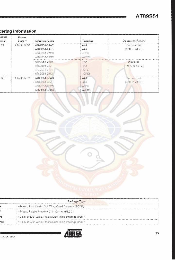
:fering Information
'6
Power
4.0\! to 5 .S\"
4 .5V i(: 5.5\.:
j:.. i S9S5 "1-24AC 44A
,!:.I89S51-24SC 42PS6 a_ "" ........ _ • .-... ~ • . ;.;. : c·::.,:;::.·::. 1-':':':';'.:";:
?:TB9S51 -33PC
44A
I'.r.~ c. ~~.: : ....
44-!ead. Thin Piasilc Gu:i ~ng Quad f"iatpack (TOF"P i
44-lead, Plastic j-ieaded Chip Cnrrier {FLee)
AT89S51
25

:kaging Information
~- TQFP
:;;\1
- 8 PiN '1 iDENTiFiER
E1
D
,~
-L-!~ -r " - - - ----_. ------~--
A'L
,is pacKage co"fG,,,S m Jt:i.Jt:,-, iefere:;ce i'v1S-G26. Va,iat;c.n .':::"C8 2 Dirr:ensiono; 01 ~:md E~ do not !n.G-'=_;de mold :xotr.Jsion _Ajlo..,.,,;?,bll"?'
protnJSiull is 0.25 rnm per :-ji(!e. Di(nellSions 01 8illj El {iie max!itlum
plastIc L'{"}\jV ~\Z8 dimRrlSion::? \nr:!ud\ng mo\Jj mismatch
TiTLE
-A
i SYm80L i i¥ii~ fviAX NOTE
A 1.2D
U.Ut. !),"1!J
_A2 '1 0:, , . , . ,------1"-- ----,------~,- --,----, o 11 7:) 12.00 j 12.25
0-: 9.90 ! ! CLOD i'~ote 2
11.75 12,00 --l'),:JrJ --
E1 9.90 10.00 10. '10 Note 2
B 0.30 0.45
c 0.09 0.20
0.45 0.75
10/5/2001
DRAWING NO. iREV. 2J25 O:-chaiG ,,--: ... --..
, 'A' .. "'"'-"7 44A. 44-iead, 10 X 10 mm BOdy Size, 1.0 tli!"!i. Body ThlcKness. \ ~ i 0.8 mm Lead Pitch, Thin Profiie Plastic Quad liar Package (TOFF)

-PLCC
1.1 4(O.C:45) ;:, 45
~ ,--. . --~~~. -~ 'r .
____ ~~C-----------~----------~ I
e.51 (Q.C20)MAX
4:') MA..'\ <3X; , •
.. /
~ ~
~ t..:-=f-:
-.'--','
.~
.. ~
,-l;=-.~
-T '- ( ~:
'-:-~
i"'l :~,
;:::--::h i:i~ "! ? ; .. ~:
.'::'.!iO\·vable prc!!lJs ion ls .C:1{},,~Q . 2 ~-4 mIT:} per sjde. Ol!'r:S':ts!on D'~ and E 1 l!iChlde mold mismatch and are measure.j at the extreme
TITLE
AT89S51
n 1~1(00075 ':
~. --, ~ , ':.' -----~,
---:s:-~~.
---- :~ 42
.- Ai
GOMMON DimENSiONS
SYMBOL ] !
A
Al
MiN
4 .1:-;1
2.286
.r..'2 0 508
17.399
NOM MAX
3.048
17.653
NOTE
----~.
D1 16662 NotA)
E 17.399 17.653
=4.9·56 16.002
:J.33:J
.. 27:J TYP -_.- ----- -------'--------'
REV. 2325 O :chard Park':!:!:::y ~~n .!n sp. C~A QS11. 1
44J. 44-iead. Plastic J-ieaded Chip CarTier (PLCC)
!DRAWING NO_
44J B
27 -MiCRO- i2i03

16-PDIP
Notes:
-11I1ii..
81
~- E
PiN
, ---1-
El
COMMON D!MENS!ONS
(10 - 15° REF "-~\\----
-1. This package conforms to JEDEC reference [\°'8-0-1-1. \iariation ,A.,C. -: D:mensio:-;s D and E 1 do not indude moid Flash ·:Jf Protrusion
t SYMBOL! NUN
... '~'- . -'-- --+-----
52.070
::1,:";:1:"; ----+-- -----+-
:.£]41
e8 15.494 i --+- -~--
MAx. NOTE
:"i::;tSL
u.:..::;s --f-- ----+- ---;
i .65i
i7.526 --+- -~,
2.540 TVP
l".T89S51
TITLE
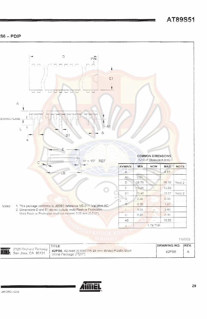
4QP6, 4U-iGad (U.oOO"· 15.L4 :mn VV:;J8; Plastic Dua: i:-:ii::e ~:;:ck8ge (rD1P
G8/28/CJi
DRAW!NGNO.
4DP6
jREV.
i B i
AT89S51
'56_ PDIP
i\iotes:
-W i;
, L
81
----!
~ .
Pi N
!
-1. Th;s package conforms to jEDEC- reference MS-011. Variation .A.D. :: Dimens!ons D and E 1 do not !r1c!lJde maid F!as~ or rrotflJS!On.
E1
COMMON DIMENSIONS
;~:S_Y_M_._8_n.c- ~!··+-_M __ IN __ ~ __ N_O_M __ +-_M_._A_X __ ~N_O_T_.~ __ ,
--\
;:: : ;3_~5 ;-- ---i·------+-
- ~.--
~ 27
G
~----L= __ 1 ____ ~~8.~. ____ _ .: .
C : .73TvP
T:TLE DRAWING NO. REV.
S2!""! jose, CA 95131 42PS6, 42-leaO (O.600';j15 .24 rnnl VVlde) P!astlc UUB: :::l~::e P2c~.5ge {rD~r"1',
AlmEl
42PS6 .fl.
29

mel Corporation
325 Orchard Parkway 8n .Joso, Ci\ 95131, US/\ el: ! (408) 44 '1-0311 3X' 1 (40R) 4117-2600
-01''' tmEl Sari
cse PQsta i€ 80 :H-1 705 Fnbourg ,\:vitz2r\a.nd 'B:- (41 ) 2S-42o ~ S5GG
~ .... (4 1; 26-42€--5500
:oon: 1219
1 ••• -•• ·• :... ••••••. • " -" 'i:i " .'-" ' :';;
· ~ 1· :"852) 2721 -9778
Cl.~ .. t852) 272'2.-1369
iiii
-24-8 Sh!:1Ka"i-la
apan
2:-:: (8 1) 3-35.23-7581
Atmel Operat ions
.\-'[e1flory
2325 Orchard Parkway San .jose. CA 9 51 :3 1. USf., Tel: 1(408) 441-0311 Fax' 1{4(8) 436-4314
Il.ii('n.;(-{in i TV; ler:
S~ r; :..!c:~e . C.A. 95131. U·Sf:-. Te!: 1(408) 441-0311 i-ax: 1 ( 40Jj } 436~4314
BP 70602 44306 Nantes Cedex 3_ France Tei: (33) 2-40-18-18-18 Fax (3 3) 2-40-18-19-60
. .:1SICfliS5PISn1! lri Curti:::
Te l: {.'1:l ; 4-42 -!j~ -hO-OO
Fax: (33) 4-42-53-60-01
1150 E.a;j~ Cheyanne- iVii.ii. 8 ;;:;J. C::j:::;~;"~:! S~!" !!"":G !=' .. ~() R.nQflh . L!~/\
-;e! 1(719) 5?6-~300 F::::x : 1(719) 540- 17~H
SCGi:IiS;-: i..... marpiiS6 I acnno:Ggy ParK
r-,..1Z:X'.A·:'::; 8u;::j: ;:9
Cast Kilbride G 75 OOR, Scotiand Tei : (44) 1]55-803-000 tax: (44) 1355-242-743
RFIA ltt(}m.otivt~
Theresienstrasse 2 Postf3Ch 3535 74025 He!!bror!n , Germany Tel' (49) 71 -31 -67-0 Fax: (49) 71-31-67-2340
Te l: l (7 19) 576-3300 Fax: 1 (7 '19) 5 4 0-1759
High Sp:"'£'d COnv,-71:",,::jRF D,~!;;,-'£~-n: Avp.nu€ da Ror: hepiei:te
!:lP 123 3852 1 S8int-Egreve Cedex. France Tel: (33) 4-76-58-30-0U Fax· (33) 4-76-58-34-80
3!meC ,n,lm:::! C:orP(:rd-;((;:: !""'!":';!-:ef. nr) ','·.-3.[:';::ly· !ur the l! ~E: 6: !tS prn(!uc.ts, utr'!er tt:at: t~Q5e 8.-::preSf;!j' CQnta:neC ~t"'l !t":e Ccrnp3.f1Y's $tar:aarc !ilty \.yhich IS detnii(;.r; ir .A.tmers- Ic-nH.'5 Dr-a Conciitir.1[1$ iocateci Or'; ttu.~ COmp8f'y's ·.·.:f:'.tl ~:He. ihe C Or.·1j)8riy (·H,~urneB rV:: :,e.:;;pnf1~if.!!Ht"r' for Cifly ~ ~vh~ c;; msy appear iii this d.:;..:umer:c. reserves In.;; r~gr: t tv .:han·;ie d:;;',fices or specificat1·:;ns dera iiea her-e irl a~ any time 'H[~hoUI t:0I1C-e. and n(:t :Yt;-'!i-,~ ;~: .:: ~·;t")r :H) ·r :!:"n(=: (:: ~(J uPdai~ ihp. :n:nnn~-l::()(: ~;!)I~ ~.~j(:t".::"l !"It::I'~t!L :-lc: i! t";nnSl~S tf) P;!i~::1: :'.. (:( t"JtI1f::r' t(iip.!!:~ct::;j! ;·l! · ~·:pf::(t~· n1 .41":·:":(:1 ar'~
=)(j by the C.0mt.:f<Pi !P r,: cf1m." r~~t i(_:n with th:~ s<::ti(' (:1 .A.tm:::! Pfcdur.:: ts. CY-Pf'::s:::!y or by ;r~"lt:l!icf1t!:.:-:n .A.tnl'-'1'~ pr::'li:.;:..:tS' ~H'-' "Ot <:il'~hGrIL8d for U$:::.' tical comp0r:.ems in life suppe:rt GBV\(.E;3. or s,:.'stems.
mei Corporation 2003. All rights reserved. Atmerto and combinatiql:s thereef arft the regisi:ereG ir3damarKS -of Al:r:1el Corporation Of HS d;ar12S. MCS·:;· is a ;;ggistl?r.;.j ;:,anBmark .::if jntB! C·:,roora;:ion . A.jobe'8 3nd A,:robat:s: are the i€gis[ered trader:,ark.5 ':if Adobe Systems inc.

SEMICONDwl...... TOR -i'
8D135/137/139
Medium Power Linear and Switching Applications • C.·JmD!Ementto OD1 36. 8Di3.'3 and 8D140 ;eSDe.:t ··;Eiy
NPN Epitaxial Silicon Transistor
--,
:::mirre: 2C(;::!ect(;:: 3.8ase
~_.~~_··"· _________ m _____ _ _ · _·· _ ___ ._~"·~~~ ____ ------.• -----.-~"-- -r-.-'----.----- .-..... ~-~. _. '- -''''-''-Sym bol Pa rameter Value UflHS
: 8D139
: 8D135 45 : 8[:; ~·7 : cw ..
----- ... - ... --f------;, " ---'-~A'
.~~.~ .-+-------
8ase Cu:;.::;n!
-----+,
;~;:;:~ :;~::: : :~ . .:: :;:, .,. ::~: :
.. ~.
::- = -:;'~"" .-.. :':::. = ., ;:-.;,,::.-.:-:
j <" '.'
h;:E Classification C!~ss:f:catQ:,,! :.3
-----·~~~,~.---~-~~-----~---~4~C~. -~1~C~.C~. ---+-----~~~::~3--~~-----+----~,~Jc:u--~~~~:I~~;---------_.----'-'-"--- ------~------.------- - ------
[D 0 -
(,,)
Vi --(,,)
~ --(,,) \i:j

Typicai Characteristics
._--- - - - -~[) j ---------, ::;:::
1 - .. ; i ,~ ,
~
~ :;;;
~ ... \
" , , ~
",: .. --~---.
Figure 1. DC cu!'!'ent Gain
" , , i 1
v., i , ~ ..
..
e.6- i
0.5 i i
~ ~.-! !
t ... 0 " ~ !" .J .,
Figure 5. PClwer Derating
1';(; i , I,,;, ...
> ;.;;, j -
-~'t' ! ..
.. ; ~ .~ i ! ...
... -.. ~ ~~
" i ;;" ~
Figure 2. Goi!ector-Emitter Saturation Voltage
:-'
:-" t '"1 ", .'--------,,-----....l..i~c----'
m o
r·--- - ------ ----- - ----- - ------ - ----- - --- ------ - --- - -, Package Demensions
lU (0 a /,,-;.. n f • --.-- --:-- -
\<-./
; l l 1, • • ' ! I -l-T
.---f-:-. ! i i ! !
2.28T':'P
: ;
~
! i
i!
_ L..., ! !
i !
n il - ~I , --,
t __ _
Tn-1?-v~ . - --
-i~
~. ·5
;: -,-,-
' ; "
,-:--, , _:l~ _
jj
.. LJ
2.22! YF ~) 5[: =~ . ~:.:: . ..::&..:.G_2;}:
OJ o

TRADEMARKS
tjottomless :1'.~ CooiFE r :;.~
FACT Qi.l~et S~ri~S TM FASP FASTr"':-"'; GTOiM
DISCLAiMER
HiSeCTM tSOPLANi\K fv1!CRO'vViRt: ::.' : ~: ..... ::-.... -
QSTM Quiet Series™ SuperSOT'M-3 SuperSOT"'-6
SuperSOT"" -8 SyncFET I ~.l
! my Lug!c : ~.~
Ui";:. ...... · ···
U:~\8!UTY AR!3!t-JG OU T OF THE ,IlPPL.!CA.T! O t'-J OR USE 'J~ .'~.t'-JY PRODUCT OF: CiRCUiT D~SCR!8ED !"-!ERE!t'-l ; NEi THER ODES iT CONVE'y' AN'{ liCENSE iJi\iDER iTS PATENT RIGHTS. t~GR T -IE RiGHTS ::::F DTI leRS.
UFE SUPPORT POUCY
FAiRCHi LD'S PR ODUCTS ARE NOT .A.iJTHOR\ZED FOR USE .AS CRiTiCAL CCIMPONENTS iN UFE SUPPORT
1. Ufe support devk:es or systems are devices or syste :ns vvh!ch, (a) ai6 intended for 5urgicai impiant into the body OJ fbi SUDP0!'"t (If sust3in life. r:;r fc! Yihose TEi;:Jrl? to r.-e rTo,m
PRODUCT ST.u..TU5 DEFiNiTiONS
Oefin,hon of Terms
r----.~---- ----.., i D.a~;h=eI ~de::t~f~:::tk.: ::
2 .. A, -:: ritica! cornpone!"":t is ar:y c':O!T':D0!"!ent 'Of a !!fe support device c,r system v .... hose raiiur€ te· perform can be ~,=asQn3biy ::;o:,pectea t::: ~9use the fa:!u:-= of the iife 'S:_;~pOit :::~~::-::. ~f "'"'f ........ :):' !:'"~ :-:ff::::: :t·::. :-;~~:f:-:~ ~ . :,n:~:::!:~:-·:'":: '·::::
--------- <--- , D:t!r:fth:::: !
Suppiernentary aata ..... -.'~!i be pUDlished 2t a iste: date !="ajrchiJd SemiconaiJC!-:'f f 13-5et}'BS the ;;ght tv make chaiiges at a;,y time ;..vithc·i.it ;:e-tice ;;, vider te- ~;;;r.rV'ye
dE~~~::
Se!l!!conductor reser ... ~s the f!g r:r to r.:ake ·:har:ges a::

SCHMITT TR'GGFR~ DUAL GATE/HEX iNVERTER
Th::: SNG2-LS 17 4LS ~ ~~ ;~:-:d S;-·JC....1LS i 7 -<iL S 1.4 c:::: :-:t~-:::-::(::y (: 9Cl~(::::; j ::-:',:::'::'t8 '-':
~'{r~:c: r: :: ~.;:.:ept staOid ar:,i TTL :::P'.J t s! gr:3.~:: 3 r::j prov\de -SlS nD8.rd TTL 0~-,tp ;..: ~
! f:vs ~t. Th 8\f ?::B cap8t:~8 elf ::?nsfc;n:;~ :-:q s l:-:\v;V ch~ :-~!l ji-: q ~!-:n: :: ~ i fln8l s ~:-: tc:
s' !1,j a phase- sp ~;tte: d!';'·..::::g 5 TTL te:tS:T: pG\s 0~tPUt . Ths S-:r:r::\tt trigger :...;~=:::; ;X:::.: i; '~·e fB8G~;:-~Cr-; to I?ff8:::t: .... t!\ ::'P8t=::; - :.:;:: ~,: t)w :nn .. :t t:i..."",; :-::E. ; ~ ;:) :~:~. a~-l d p:'ov;ae
different ir:put thresr-:old '·;oitages fer positive ar:d negative-goir:g trans itions. T!~ ~5 h\'St8 !'"8:~,~~, ber ... veen th8: ;;r:Sit:V9-qoi::G ,,:!!::~ ;-:eg.?ri'.'e-qo;;-:q ::-:Q\jt
!~: :-:,;;.;; l i\..:lcj::; (tjL":"~ '; :'/ ;::i_:C: ", v I '=" ''::;V_' :-''' '~ ;':; , ; ;t~r;: i:l~ ~y L:y ;-;;:" :j, ::; iv1" 1"!:"; i:r_:,=" ::, "":::
-F::=:~A::tl:;~! V !::~s:: s~ t l'· ... ~ t::: te!T!ps;,qt:..;;s .:::: r:;-! ~!iPp:V '..:c; l t~~:3 '..·· . .;:L.;t ; :::::~
5N54 /74LS13
i "'-,
r-r===~~~~I U .~ ,---'
I i I • , w j-j -' _._'
ilCc.
i~ _..1,:: .. :, .
"SN54!74LSi4
1 : ';.1 ~ 1) ! • 1" "'_ • ' f '-' ,
l:-_ ~ Yfi'.>:--
,_;,,' o,! . ~~
::! 1::1! ! c< ~:; i p ..... _ .... ~ ....... 0...- ........ . • 1 • • ~ _'- • • " . ...
: ,_. _ . i f_' _ i q~_~-l q~~>o-J
I : f , ! ::'! 1:· . i 6 l
'- -'
GUARANTEED OPERATiNG RANGES
SN54!?4LS13
r--.--------------------------~
i SCHMITI TRIGGERS
DUAL GATE/HEX iNVERTER
LOW POWER SCHOTTKY
J SUFFIX
N SUFFIX
o SUFFiX
ORDERING INFORMATION
:':'::-''::-:4 :. :~Y.X.i :}i··; 74L.S:t:::I:>l
.------------,------~----,-----~-----.---~
?3:==:::1ster M~:: Tyrp M.ax Unit i \-'CC~ ! ~:..: :..: :-;: y "~;"0~~age ,
l -~~'''"' i Cp€:-.~tir: g .il.;:::' :.;::::! T~::·: r·+'L';~:":!'~ R.ar:g-::.
! ',,---.-,""~'"~"" .," t"'·
,' , ;;.:.;
74
DATA
:)-;
::, . .25
. .::::: . ··~ t ,-· ,-.. ,,--
i
.. ·.,i
!
G.::;

SN54!74LS13 • SN54!74LS14
l C CHARACTERISTICS OVER OPERATiNG TEMPERATURE RANGE ,<.r';~". c:-,~p" ,,~ ,n~' '.6"
\' :+
;';OH
::1;):.:: .. .... .... . , .. :'::
C CHARACTERiSTICS i
\.': :.'
Q.6
74
Limit:;
J.4
:::.15
i i _ tl 18 i _.
.2.9
L.V
6.0
:....~~ 4 j ~.:.; ! ~6 I. "" '" .. ~ ... i· ....... ,:. - . -"' I', i LS~:3 1 l ~ .. ' i 1
l'~~'~--'--l-'-;-'-f-;--l ,
27
---.~------.---~-,.\ :.:: -f- ... \'-___ _ ___ -'l
flgure 1. AC Waveforms
\fcc = 5,0'
'~----'-----'-"----
5-2
"' - .. "" - ~. '-'

..,.-- -'
,~
SN54!74LS13 • SN54!74LS14
5 ! r 1ft.:= 2:·:::::;
4 rl--~~--:~, ---+i ----~-Ir+--~----~--~,----~!----" 1··----- t--'-- ··+·_·t ..... 1" . --,.+~ --~~-- -~,:". ----1
i ! , !-' --'----+-+ i .!
! i ' i i, • 2 ~i ---t---,+l ----~--+_4++,-_+_----'---.i---_+! i i I ' !
, j~__+_--~~_+_HI:--+_~~--~:~ --+- . i----. : - ti.,; , .. I--,-----i-+--__ '-i-_--i __ .. ! _._. --'
t; i:,
Figure 2, VIN versus VOUT Transfer Function
, : : : : . : i--+ ---4-~--+---4--- '~---i~
Figure 3. Threshold Voltage and Hysteresi5 versus Power Supply Voltage
. :) r, ---_--_----_--.....,.----_--_---_---,---,
.. ~' --'----'--- -'------i- -!--'-----+--+---f-- --~; --.i---+-"-~;--+-. . _~' _ __ .i ,-~---~,~
i
Figure 4, Threshold Voltage Hysteresis iiBrSU$ Temper(iture
FAST .t:..ND LS TTL DATA
5-::>

=-" AlNalional Sern co nd UCtor I .. /'i'"
':f!ith sevara! fixed output ~.:C'!tag€s :ra.king the::: useful in 2.
wide ran~e of appiicanons. One of inese is iocai on card ~e~~!:~!;cn, e!::"!'":i:-13!:n~ the di5.tr:!:!u!inn ~f~~!9~r:s 3SS0Ci3!ed '.-,:':; ;; t .::':q:0 p o:::: :-(;Q :.; ;~:::::;: ': if:0 '.':...:: :.<1;,.(\,;::. ....... : .• ;::..:;;;,; ;,,1.:::.; .......
th:::.~:~ 1:! rel~ ~_t! ~. trJrs to ty::.! used ;;; l(lIJ;t.:: :;v~tf::!rns. ir.8-!.:IJ!r.t:!r,! . .::.~
tior. niFi. ani] olher sO!!d state electronic eQuipment .Aj-
devices caii be used "viih aAtamai cOi7ipc-nents to c-btain adl:..:st2.b!e '.,:·:;::t.=.ges and cu:!"":::!":ts.
Tht::t :.. 1'I.~78':('X '::-J? r ~s "S ;'!'.::a.' :lC 8 :'. :l""l ;3.!'..!:--,:r:un '1('··3 pa'':K
age which yviil aHow Over 1.0A load curient if adequate hEat si:1kjng js provided, Gurrei:t iir::it[ng ;s inch.lded to lim;t the peak Qutput cur:s::! tc, .:: sa7e \;al:":5, S2T5 2:e:=. pr0te·:t!o!1 ro: thf: ::utput ! !"" ,:: r:Si2.t0: if> p:0"j!~~d to :im;t inte:~"!~! pC'N5r d!~s; ·
p;:~tjon . 11 mternal pmvet' ri!BSlp.:I tion bec.ort1t"lS too hinh tOt
me. heat slnk:nq f)fO·.;:ded, U,e tn ~:'irrr:31 si"lutdm· ... r: ::::~8Uit
Schematic and Connection Diagrams
output, £:!though this 0052 irnpra'.ie transient rsspor!se. lr!put bypassing is needed oniy if the ragui.:;,tQf is ioc3teri tar from
;::~r ·:::.:tP:Jt "!0it 2g<s 0lher than 5V. 12V an·oj ~ 5V the U·A ~ !;"
s€:ies p;,,:;'·.: !-:e5 =-:": '':~~i-':'':~ '!0itage :.::::ge fro:-=: :.2\1 to _': '.:.
Features • OUlput currant in excess of i A • lnt:3rnai th:3,mai overl0ad prot.ection
• No ax!err.a~ componer:ts !""equired
Voitage Range
Uvi/3ioi";
l 2V
Met~! Can P~~k::!!Je TO-3 (K)
Aiuminum
Oros: Number Lf .. 17805GK, LM?312CK or LM?8iSCK
See NS Package Number KC02A
Plastic Package TO-220 (Tj
Top View T: :!-;.': 1'::;:- _ ':::
Qrde~ Numher LM78;jSCT~
LM7812CT or LM7S15CT See NS Package Number T038

Absoiute iiiiaximum Ratings :: M'iiii9 ry'i Ai:(~~pit(ot: :op-i:(;iiitu ~'ii(;t::; ':f£: f~u:i";-j ,
;!iease contae! the Na!!onaJ Se~l-:;~ld!...!cto!" Sales Office/OfstnOutors for availability and speciti-cauons.
:;'C: to i- 70:('; TO-3 Pac:kaga K TG 220 P ;1;::-.;Al:j:": :
Eiectricai Characteristics LMl'8XXC (N,,'.2WC <C ' i' ';>5OC;m'Oi;; cthe., <"'S" "o!eo,
__________________ ~O~"~'~p~u~t~V~O~!l=.~~=. __________________ _+----~5~V------C_--__ ~1~~V~ ____ +_----,-'-5-V-----__ j
\ ______ ~, ____ i_np'-u_'_v_' O_!_'.-,o-,.---,-(U~n-ie-''-',--,o-th-.-C-w-is-.--n-o-te<i-,)----------+----~_'1l_V~ ____ ,-__ ~_'9_V~ ____ -,-__ ~_2:.3,-V--;;-__ --,i Linits
! SymbOi j Pai'ai'rlete~ ___ ~ Ccndilions ----L-~if1 t Ty~ i M~~~h'l ! _~.!:lMa~:_ i T~~~ .. n
jr.:.:utC.ut VOiiage !;! -2c····c.~!T:;... ::: iO::::1.A ! .~ .o ~ .2 1; i.':I 12 ._._ -;'~ A 151':1.6
;1\; ~ ~ 5"'~"·,5 r:-::~ :o..;0 ~ :;:.; '::,75 5.25 i t.": 12.6 \;~ i:S
~ ""\;;i,,::: "/;;'i::'" '.:;., .. :..:.: . ... - - ~':;;.;":: 2-::; ~ :.;':'5 ~ ~' ; ;-t ::'" ~ . • , .... __ ~':i1~ :':: 30:
:'U - ::..!_!:) :-;-• .=. : =: = 2:::~ :-;
i--. \f::.!
]T: =--- 25"(;
t .::, .... :;~
~fi' '-: .:, ; r::i. :~::: ~ :1:\
;2'::'J r:::'... _ .:.. ("-,r.} ~~: . .:Io.i
'-i ··iN iC·ut;:,;; :.~:;::;c .;c;:,;.:g(:j: .". - .~:rr: ,., :-;7 -. . -:.~-" .--- --l -----'
-'-'-.::'~ iR:;:C':B F;'=:j.::.:t:0::
:. :2:.iH:' \ : ~-:-,--- 5 C,;: m:~
,- .. ~~~ . .. :":; ::~::;:..;
iOutCrutp.6Slsta'-'CB i: ..... -:. ~' H::: ! ~.hr.ri ·GiiC.:.d ·:::~n~:-,,~ ;T; ,.." 25~'::: ! F ,;.a~. v u41I.!' ::"'\ii"i"t'lll ;,. - 25'·C
... '- .
__ i __ _
SC:
'v:r_l:...o·m i sa :
: . ~.::.. t",
,< <:.' +-"'-' -:..: --- ~ ::;
18
!75 '- ".' ',; :... .,;:.::
: : c::.-.
2:';
i?
2.":
- f
v
: ::~.
v
".
1\
,~
l _ __ -i)_A_< .. _c_'."r'-,"_~_.:-_, _c_,_v,,(";.c: :.c'_i),-::-~:--, ___ ' ;..'_'< ___ '_c_' _'{'_'_',,-'_-__ '_,'""_,,_A ____ + _____ C_' _F-____ -t' ___ --'--' ----i--- ___ '_"_', _____ +::-_"_'.:_' __
j !:~p:.: ! V::;::ase
;::l&Q;;;;;iC,-:. M""ntai" jTi = 2~;/G.;(; ~ ~.t... l ___ l~:r: : ; 2~~;JI::!.._'C_" _; __ ---'-::,,-,-_____ -,----,::: ________ -:-__ ---' __________ -,----:-, ________ __ ---' ____________ • ____ _
~~::::~:; ~: T:-: :::-:':""~~ : r:-:;:~: :: :":~ ::: Teo' J ::::::::::G:": _. :-; :yp::-_~::: :.-..... : ..... ::: ,.._~::::- ::: =:;:: ::.-:.:; ~::,·c.""" :';:::'"~::: :::::--::::::.-: : .
. " ~:2 .'"'. ;0 , ..

Typical Performance Characteristics
Maltimum Average Power Dissipation
Maximum Average Power Dissipation
! !
f·.L . -. : 1 +: -i-'-+-;-,-+---: : . . . ;~ tt.~ ___ ~J
tc) 1 V ;'\t T~ = 25:' (:) 1.0tO :-.....,--~--~--.,--~ ,
; 1 (;~)
~ f,'!li!i !
S :) Sgu
~ D,S!!: :
:; :j~tSli :< 3 ;:;.37!:
"
-----......;,. ' -", .
--. --~! ._" -~ '--l
~.
i -------+--1
0;" '---'~~---'-~-'--'
7~ ~.. <_.
(luiescent C!)rr~nt , ., ~-~~~-..--7.,--,._-, ! : ; i "oj.~: - H!'.'
~ . ----+-------+--t - Ii 0 U f ~ ;: I. -f
: .. ,. : , 1 ~ l~ ____ '_~'_~, ~:_ . . _-'
- :~ 50 1~ '} 25 51) l ~ lOr) 125 l SO
JUN CTI ON HY.fI~R;\TJR E i' C)
3
',\i
,:,'·'UU r - ifJU . n~( j _ . . "--.
. -,-.
~ I::": : ~r • • "
\:VUT - ~ii
:~:.:r" 11111'.l
--- 25"£
Peak Output Current ;'J
i - - --- ---;----; • -----1-- :
, "-'---;--~
j ~ 11!: tu
ED }- 'ijii-vUiJf" :i '.in:: . l~ \.':~ ! '--i ; : ;";::! ~ : !. ! :, "."'/::::"l. -i 1
JJIf ;~',,; ~ )C:l~~ ~
f-';-+-"'''''c.'::~;' j n ~ JT :~ !A, - - i r-' j- i--i--- --j
- -.


Physical Dimensions inches ,,,,iilimete's!
: ",<Ii) -u.9II0 i ~: j::::UiE- 24 .S3j .~
(2,718 -3 124;
{] 025
:.3 .500 - ij . oi~
~10.:!~-:!~ . :~~ OIA
T , ;, .,
[il635l--· 0.135 f3.4291
: ~~r:n? ... : ; nu .. rn =-EAn n::t
G!A
. ! -H e.25f1-il.J~) , . !
!i
. r~-----'~~H' :------~·--d Sa
!! \ • il SEAilNij PlAIIiE
OiQ TYF
0.420-0.440 .. ~ -- -- ... j;" ' ;;; - 1;, ~ .. ;
;ii .:m -13 26)
0.155 -0.179
,4.19' 4.5471
U.37iJ-i.aso
, ;] .555 - U.t;l .-LH7-L ~g? - 1 ___ _
{Z9.90-JO.4nl 1
Aiuminum Meta! Can Packagl! (KC} Order riumocr LM7805GK! i...fvi7Bi2C~ O'f LMI8i5CK

I/) ~
o -C'\'S
::::J Cl CI,)
a: CI,) Cl C'\'S -o > I/) CI,) 'i: CI,)
en x x CIO ..... :E ...J
Physical Dimensions inches (millimeters) (Continued)
LIFE SUPPORT POLICY
TO-220 Package (T) Order Number LM7805CT, LM7812CT or LM7815CT
NS Package Number "038
NATIONAL'S PRODUCTS ARE NOT AUTHORIZED FOR USE AS CRITICAL COMPONENTS IN LIFE SUPPORT DEVICES OR SYSTEMS WITHOUT THE EXPRESS WRITIEN APPROVAL OF THE PRESIDENT OF NATIONAL SEMICONDUCTOR CORPORATION. As used herein:
1. Life support devices or systems are devices or systems which, (a) are intended for surgical implant into the body, or (b) support or sustain life, and whose failure to perform, when properly used in accordance with instructions for use provided in the labeling, can be reasonably expected to result in a significant injury to the user.
2. A critical component is any component of a life support deVice or system whose failure to perform can be reasonably expected to cause the failure of the life support device or system, or to affect its safety or effectiveness.
National Semiconductor Corporation 1111 West Bardin Road Arlington, TX 76017 Tel: 1 (800) 272-9959 Fall: 1(800) 737-7018
NaUonai SemiconductOt EurOJ)@
Fall (+ 49) 0-180-530 85 86 Email: [email protected]
Deutsch Tel: (+49) 0-180-530 85 as Engrish Tel: (+ 49) 0-180-532 7a 32 Francais Tel: ( f· 49) 0-180-532 93 56 Italiano Tel : (+49) 0-180-534 1680
National Semiconductor Hong Kong. Ltd. 13th Floor, Straight BlOCk, Ocean Centr6. 5 Canton Rd. Tsimsha:sui, Ko\llloon Hong Koog Tel: (852) 2737-1600 Fa.x: (852) 2736-9960
Nation.1 Semiconductor Japan Ltd. Tel' 81-043-299-2309 Fax: 81-043·299-2408

BIODATA
Nama : Daniel Kurniawan
NRP : 5 J 0300004]
Tempat / TanggaI Lahir : \1adiun, 20 Februari J 982
AJamat : J1. KaJijudan 2, Surabaya
Agama : Kristen
Riwayat Pendidikan :
SD Katolik "Santa Maria" Ponorogo (1988-1994)
SMP Katolik "Slamet Riyadi" Ponorogo (1994-1997)
SMA Katolik "Bonaventura" Madiun (1997-2000)
Universitas Katolik Widya Mandala Surabaya (2000-2005)
-=~~,~~- - ' -- ------- ----'--l t ~ R f' L ',' j , \ .. " \ 1\"
Univeulta. kd tU :\. t, . " . .. " .. ~ . ... . ~ SU1'A.i:\ 'lA
Related Documents