SSUET/QR/112 Laboratory Manual Digital Logic Design (EE-220) Third Semester Telecommunication Engineering TELECOMMUNICATION ENGINEERING DEPARTMENT Sir Syed University Of Engineering and Technology University Road, Karachi-75300 http://www.ssuet.edu.pk

Welcome message from author
This document is posted to help you gain knowledge. Please leave a comment to let me know what you think about it! Share it to your friends and learn new things together.
Transcript

SSUET/QR/112
Laboratory Manual
Digital Logic Design (EE-220)
Third Semester Telecommunication Engineering
TELECOMMUNICATION ENGINEERING
DEPARTMENT Sir Syed University Of Engineering and Technology
University Road, Karachi-75300 http://www.ssuet.edu.pk

Digital Logic Design (EE-220) Lab Manual
Department of Telecommunication Engineering Sir Syed University of Engineering and Technology Karachi
SSUET/QR/113
LAB CONTENTS
`
LAB #
Date
LAB TITLE
Score/Grade
Signature
1
To study the logic gates in the TTL ICs and familiarize with
Combinational logic.
2 To verify De-Morgan’s laws and verification of Boolean Laws
and Rules.
3
Design and implement Half and Full Adder using combinational
logic.
4
Implementation of 4 variable Karnaugh-Map (SOP).
5 a) To convert given binary numbers to gray codes
b) Designing an Odd Parity Generator and Checker for a 3-bit
Data.
6
Designing of a 4x2 Priority Encoder.
Experimenting with 74148IC Octal (8x3) Priority Encoder.
7
Designing of a 2x4 Decoder / 1x4 De-multiplexer.
Experimenting with 74138 IC.
8
Designing of a 4x1 Multiplexer.
Experimenting with 74151 IC.
9
Design RS Latch Using NAND gate, testing of JK flip-flop and
develop D- Flip-Flop using JK FF and T- Flip-Flop using JK
FF.
10
To study the working of 4-bit Up/Down counter using IC 74193.
11
To study parallel in parallel out PIPO shift register using
IC74273 (D-type flip flop).

Digital Logic Design (EE-220) Lab Manual
Department of Telecommunication Engineering Sir Syed University of Engineering and Technology Karachi
12
To study parallel in parallel out PIPO shift register using
IC74273 (D-type flip flop).
13
To build JK MASTER SLAVE flip flop and verify its truth table.
14
Design a decade counter (Mod-10) by using JK flip flop.
15 To study the Programmable logic devices and familiarize with
programmable logic devices.

4SSUET/QR/11 220)-igital Logic Design (EED
Department of Telecommunication Engineering
Sir Syed University of Engineering & Technology, Karachi
Experiment No. 1
Objective
To study the logic gates in the TTL ICs and familiarize with Combinational logic
Components Required
Bread board
5 V - power supply
Multimeter
Logic probe
LEDs with resistors
Connecting wires
Switches
Following ICs and their datasheets
7408: quad 2 input AND
7432: quad 2 input OR gate
7404: hex inverter
7400: quad 2 input NAND
7402: quad 2 input NOR gate
7486: quad 2 input EXOR gate
Theory Logic Gates Logic gates are the fundamental building blocks of digital systems. These devices are able to
make decisions, in the sense that they produce one output level when some combinations of
input levels are present and a different output when other combinations are applied; hence
given the name Logic Gates. The two levels produced by digital circuitry are referred as HIGH
and LOW, TRUE and FALSE, ON and OFF, or simply 1 and 0. There are only three basic
gates: AND, OR and NOT. The other gates are merely combinations of these basic gates.
Logic gates can be interconnected to perform a variety of logical operations. This interconnection
of gates to achieve prescribed outcomes is called logic design.
AND Gate An AND gate's output is 1 if and only if all its inputs are 1. e.g if A and B. are two inputs of an
AND gate then output, F of the gate is given as: F = A . B
OR Gate An OR gate's output is 1 if at least one of its input is 1 e.g. if A and B are two inputs to an OR
gate then output, F of the gate is given as: F = A+B

4SSUET/QR/11 220)-igital Logic Design (EED
Department of Telecommunication Engineering
Sir Syed University of Engineering & Technology, Karachi
NOT Gate (Inverter)
Its output is 1 when its input is 0 and its output is 0 when the
input is 1; i.e. it complements a digital variable. If A is the intput to a gate then output, F of the
gate is given as: F= A`
NAND Gate Its output is 1 if at least one of its inputs is 0. This gate performs the
same logic as an AND gate followed by an inverter. If A and B are two inputs to a NAND
gate then output, F of the gate is given as: F = A . B
NOR Gate The output of a NOR gate is 1 if and only if all its inputs are 0. This gate
performs the same logic function as an OR gate followed by an inverter. If A and B are
two inputs to a NAND gate then output, F of the gate is given as: F= A+B
All the above gates have one output and two or more inputs except the NOT gate, which has
only one input.
EXOR Gate EXOR operation is that if even numbers of binary inputs are logic 1 output will be logic 1;
otherwise output will be logic 0. for 2 inputs, it becomes a bit comparison operation. The
Output is high only if either A or B is high, output goes low if both inputs are high or low. If A
and B are two inputs to a NAND gate then output, F of the gate is given as: F= A B.
Procedure For Testing Logic Gates In Given ICs
1. Set the power supply to 5V.with the help of a multimeter check the voltage at the
output knobs of the power supply.
2. Connect wires; long enough to reach the breadboard, with the two knobs of the power
supply. Again using multimeter, check voltages at the non-connected end of the wires.
3. Insert the 7408 quad 2 input AND gate IC on to the bread board and make supply and
ground connections by joining wire between 5V and pin # 14 as well as 0V and pin #
7.
4. Consult IC's internal connection diagram for input and the output pins of the first AND
gate. Connect input pins to logic 0 (0V) and observe the output using LED or logic probe.
You can also connect switches at the input lines to facilitate togging between 1 and 0.
5. Try different combinations of logic levels at the two inputs. Again observe the output.
6. Repeat the last two steps for all other gates of the same IC. Record the observations.
7. Repeat this procedure for all other ICs.
4SSUET/QR/11 220)-igital Logic Design (EED
Department of Telecommunication Engineering
Sir Syed University of Engineering & Technology, Karachi
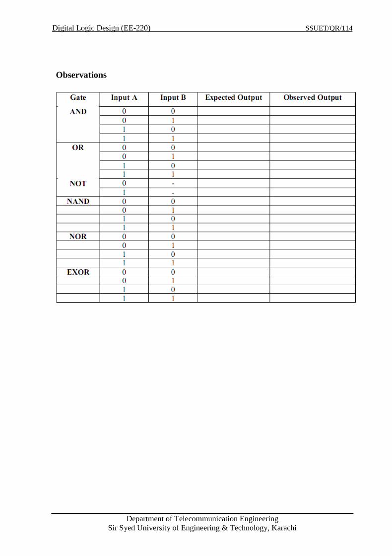
Observations
4SSUET/QR/11 220)-igital Logic Design (EED
Department of Telecommunication Engineering
Sir Syed University of Engineering & Technology, Karachi
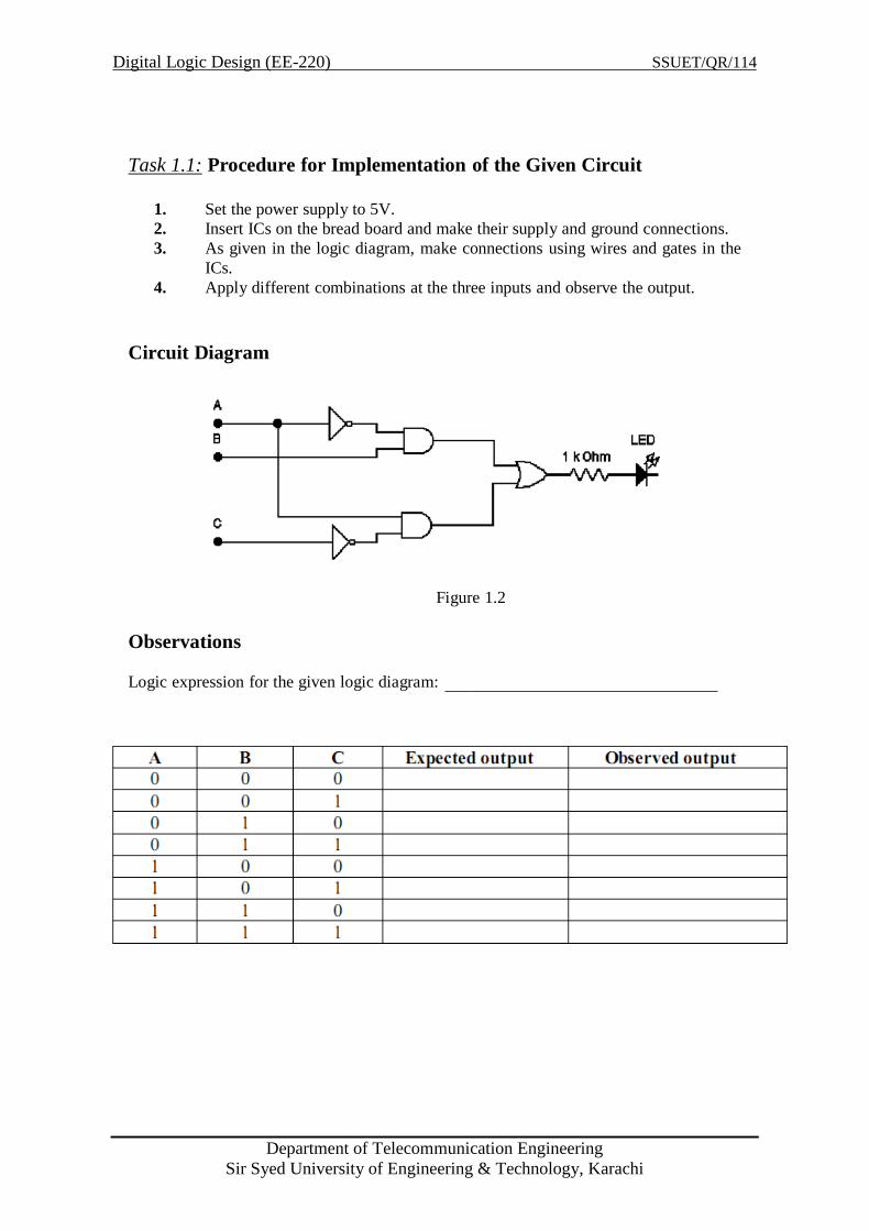
Task 1.1: Procedure for Implementation of the Given Circuit
1. Set the power supply to 5V.
2. Insert ICs on the bread board and make their supply and ground connections.
3. As given in the logic diagram, make connections using wires and gates in the
ICs.
4. Apply different combinations at the three inputs and observe the output.
Circuit Diagram
Figure 1.2
Observations
Logic expression for the given logic diagram:
4SSUET/QR/11 220)-igital Logic Design (EED
Department of Telecommunication Engineering
Sir Syed University of Engineering & Technology, Karachi
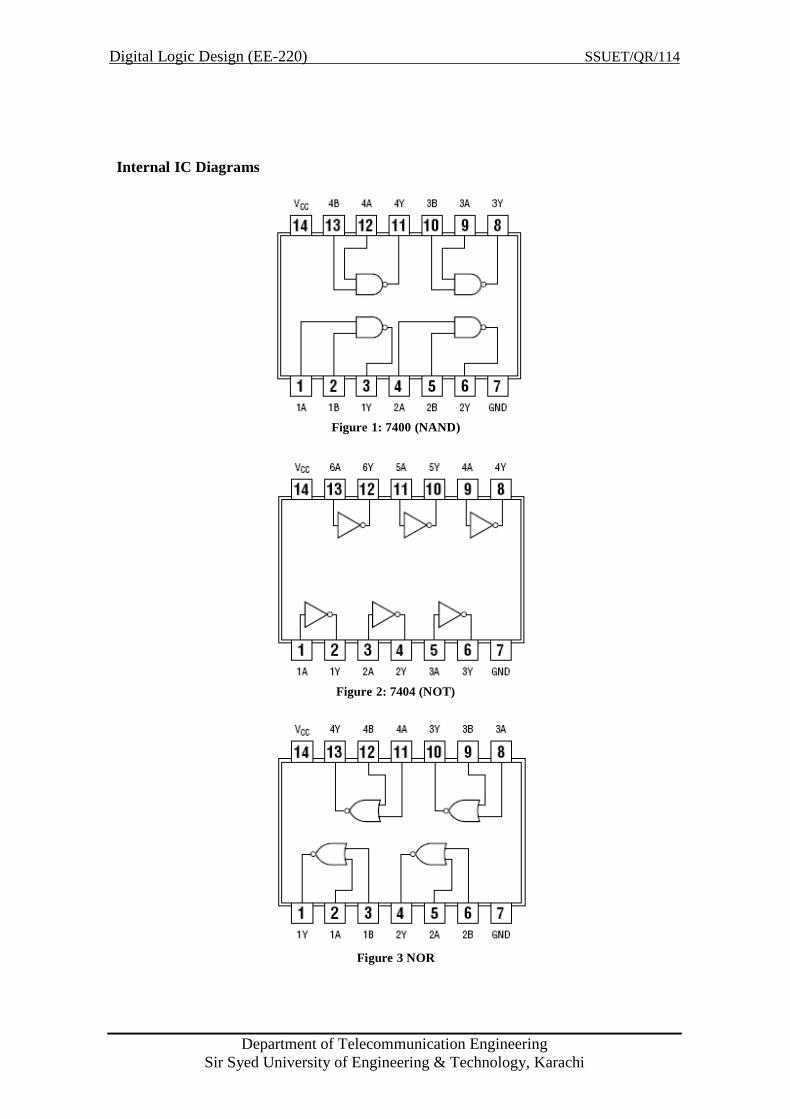
Internal IC Diagrams
Figure 1: 7400 (NAND)
Figure 2: 7404 (NOT)
Figure 3 NOR
4SSUET/QR/11 220)-igital Logic Design (EED
Department of Telecommunication Engineering
Sir Syed University of Engineering & Technology, Karachi
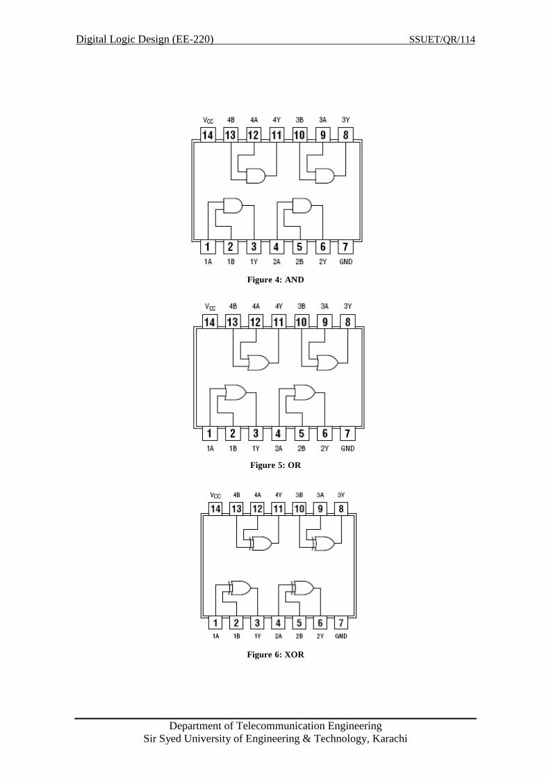
Figure 4: AND
Figure 5: OR
Figure 6: XOR
4SSUET/QR/11 220)-igital Logic Design (EED
Department of Telecommunication Engineering
Sir Syed University of Engineering & Technology, Karachi
Experiment No. 2
Objective To verify De-Morgan’s laws and verification of Boolean Laws and Rules.
Components & Apparatus Required Bread board/Digital Logic Trainer
5 V -DC Power Supply
Logic probe
ICs 7410, 7427, 7432, 7408 & 7404
Theory In Boolean algebra, the two De Morgan’s laws are very important as these play key role
in manipulating logic functions into SOP/POS forms. For two inputs, these laws are:
In this experiment, you will using 3-input NAND and NOR gates to verify De Morgan’s
laws for three inputs
Procedure & Observations
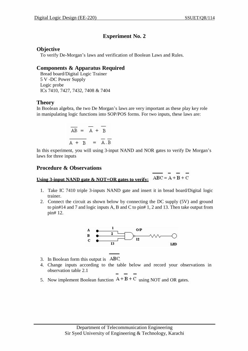
Using 3-input NAND gate & NOT+OR gates to verify:
1. Take IC 7410 triple 3-inputs NAND gate and insert it in bread board/Digital logic
trainer.
2. Connect the circuit as shown below by connecting the DC supply (5V) and ground
to pin#14 and 7 and logic inputs A, B and C to pin# 1, 2 and 13. Then take output from
pin# 12.
3. In Boolean form this output is .
4. Change inputs according to the table below and record your observations in
observation table 2.1
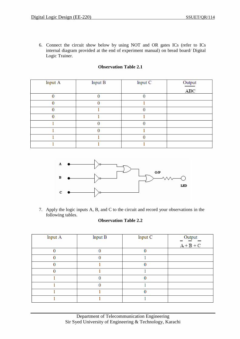
5. Now implement Boolean function using NOT and OR gates.
4SSUET/QR/11 220)-igital Logic Design (EED
Department of Telecommunication Engineering
Sir Syed University of Engineering & Technology, Karachi
6. Connect the circuit show below by using NOT and OR gates ICs (refer to ICs
internal diagram provided at the end of experiment manual) on bread board/ Digital
Logic Trainer.
Observation Table 2.1
Input A Input B Input C Output
0 0 0
0 0 1
0 1 0
0 1 1
1 0 0
1 0 1
1 1 0
1 1 1
7. Apply the logic inputs A, B, and C to the circuit and record your observations in the
following tables.
Observation Table 2.2
4SSUET/QR/11 220)-igital Logic Design (EED
Department of Telecommunication Engineering
Sir Syed University of Engineering & Technology, Karachi
You will agree that the outputs of two tables are same. Hence De- Morgan’s law is
verified.
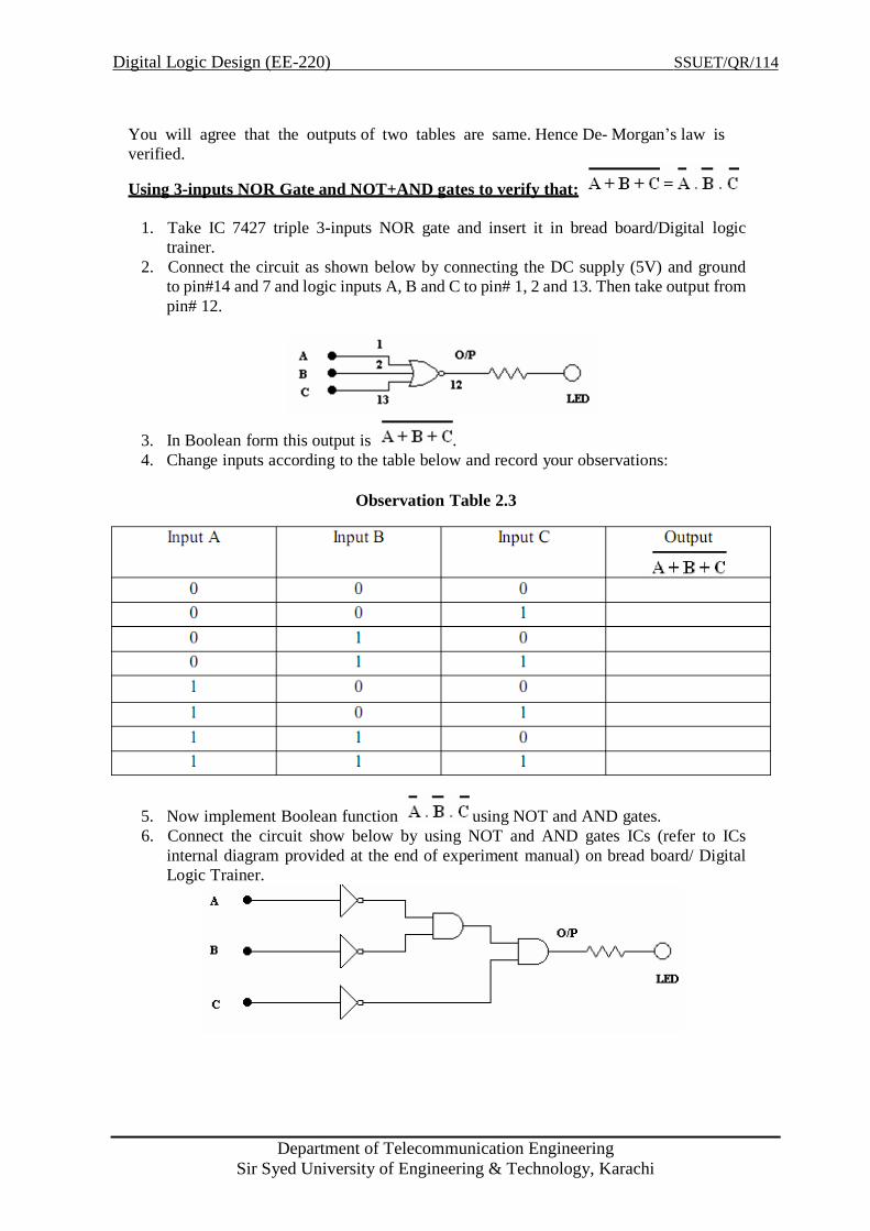
Using 3-inputs NOR Gate and NOT+AND gates to verify that:
1. Take IC 7427 triple 3-inputs NOR gate and insert it in bread board/Digital logic
trainer.
2. Connect the circuit as shown below by connecting the DC supply (5V) and ground
to pin#14 and 7 and logic inputs A, B and C to pin# 1, 2 and 13. Then take output from
pin# 12.
3. In Boolean form this output is .
4. Change inputs according to the table below and record your observations:
Observation Table 2.3
Input A Input B Input C Output
0 0 0
0 0 1
0 1 0
0 1 1
1 0 0
1 0 1
1 1 0
1 1 1
5. Now implement Boolean function using NOT and AND gates.
6. Connect the circuit show below by using NOT and AND gates ICs (refer to ICs
internal diagram provided at the end of experiment manual) on bread board/ Digital
Logic Trainer.
4SSUET/QR/11 220)-igital Logic Design (EED
Department of Telecommunication Engineering
Sir Syed University of Engineering & Technology, Karachi
7. Apply the logic inputs A, B, and C to the circuit and record your observations in the
following tables:
Observation Table 3.4
Input A Input B Input C Output
0 0 0
0 0 1
0 1 0
0 1 1
1 0 0
1 0 1
1 1 0
1 1 1
You will agree that the outputs of two tables are same. Hence De-Morgan’s law is
verified.
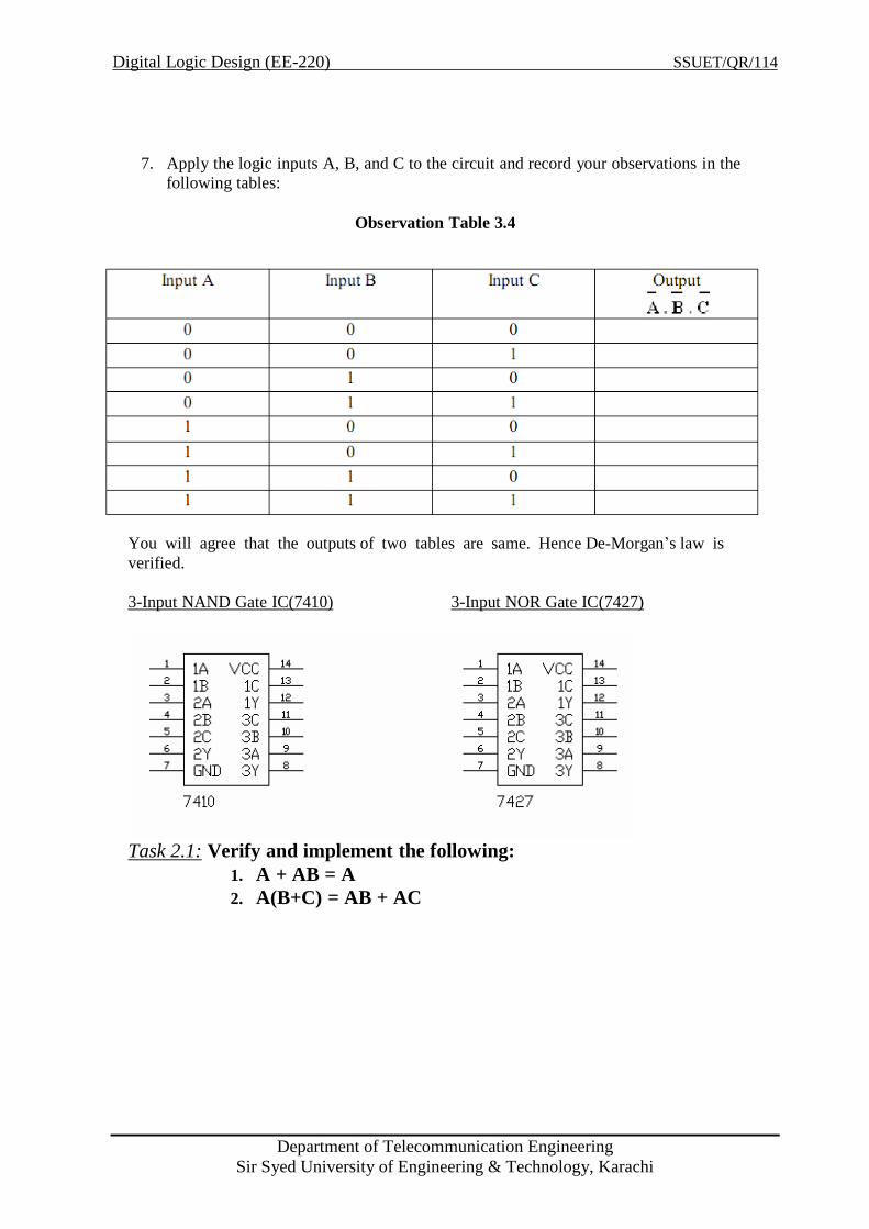
3-Input NAND Gate IC(7410) 3-Input NOR Gate IC(7427)
Task 2.1: Verify and implement the following:
1. A + AB = A
2. A(B+C) = AB + AC
4SSUET/QR/11 220)-igital Logic Design (EED
Department of Telecommunication Engineering
Sir Syed University of Engineering & Technology, Karachi
Experiment No. 3
Objective Design and implement Half and Full Adder using combinational logic.
Components and Apparatus Required 1. Following ICs and their Datasheets:
I. 7408 Quad 2-input AND Gate.
II. 7432 Quad 2-input OR Gate.
III. 7486 Quad 2-input XOR Gate
2. Bread board/Digital Trainer.
3. 5 V - Power Supply.
4. Multimeter.
5. Logic Probe.
6. LEDs with Resistors.
7. Connecting wires.
Theory
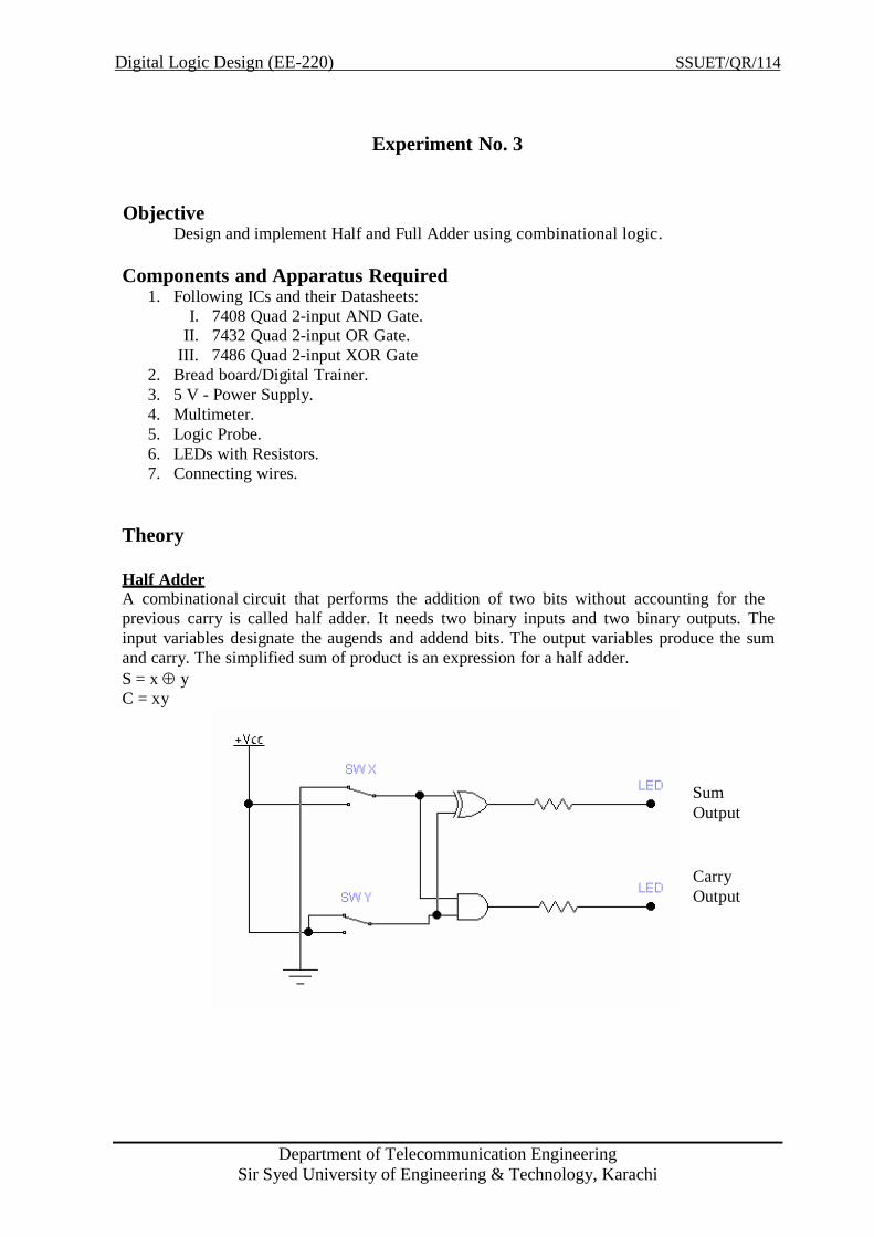
Half Adder A combinational circuit that performs the addition of two bits without accounting for the
previous carry is called half adder. It needs two binary inputs and two binary outputs. The
input variables designate the augends and addend bits. The output variables produce the sum
and carry. The simplified sum of product is an expression for a half adder.
S = x y
C = xy
Sum
Output
Carry
Output
4SSUET/QR/11 220)-igital Logic Design (EED
Department of Telecommunication Engineering
Sir Syed University of Engineering & Technology, Karachi
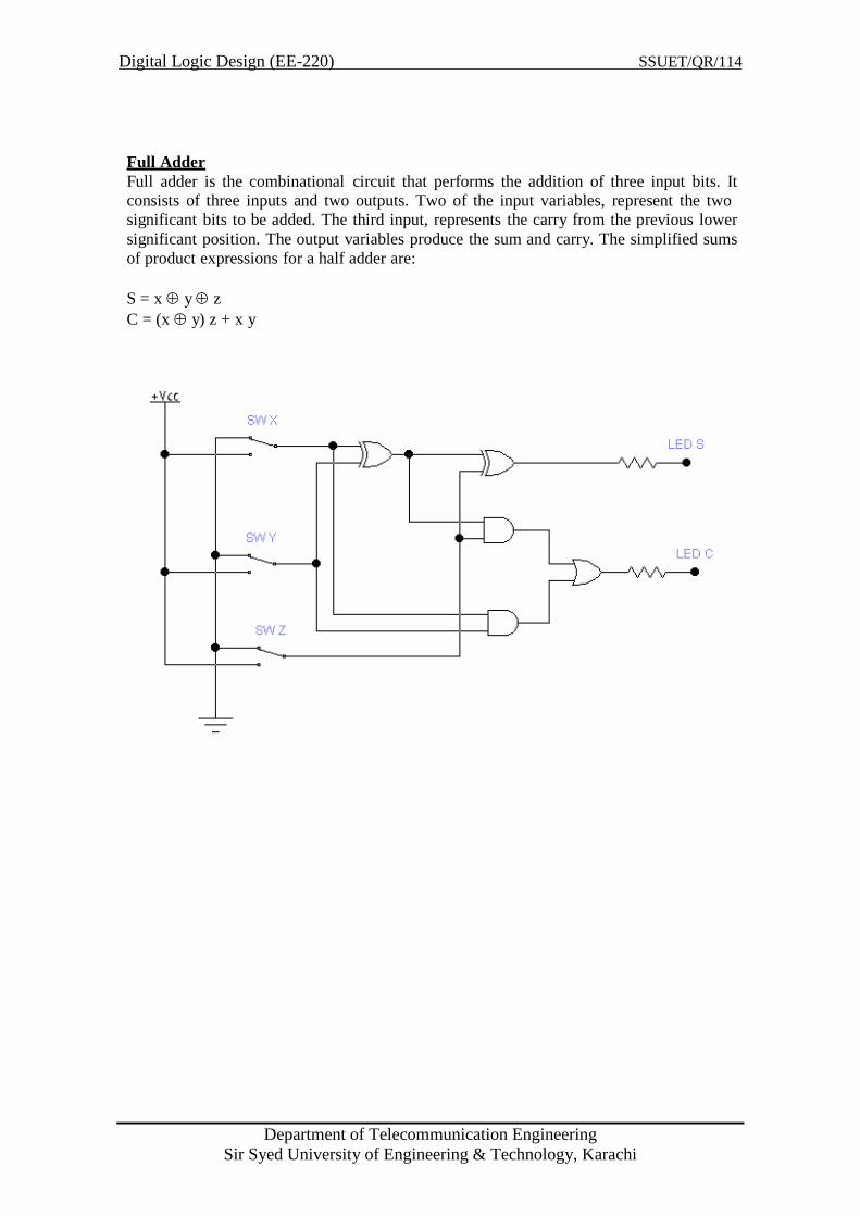
Full Adder
Full adder is the combinational circuit that performs the addition of three input bits. It
consists of three inputs and two outputs. Two of the input variables, represent the two
significant bits to be added. The third input, represents the carry from the previous lower
significant position. The output variables produce the sum and carry. The simplified sums
of product expressions for a half adder are:
S = x y z
C = (x y) z + x y
4SSUET/QR/11 220)-igital Logic Design (EED
Department of Telecommunication Engineering
Sir Syed University of Engineering & Technology, Karachi
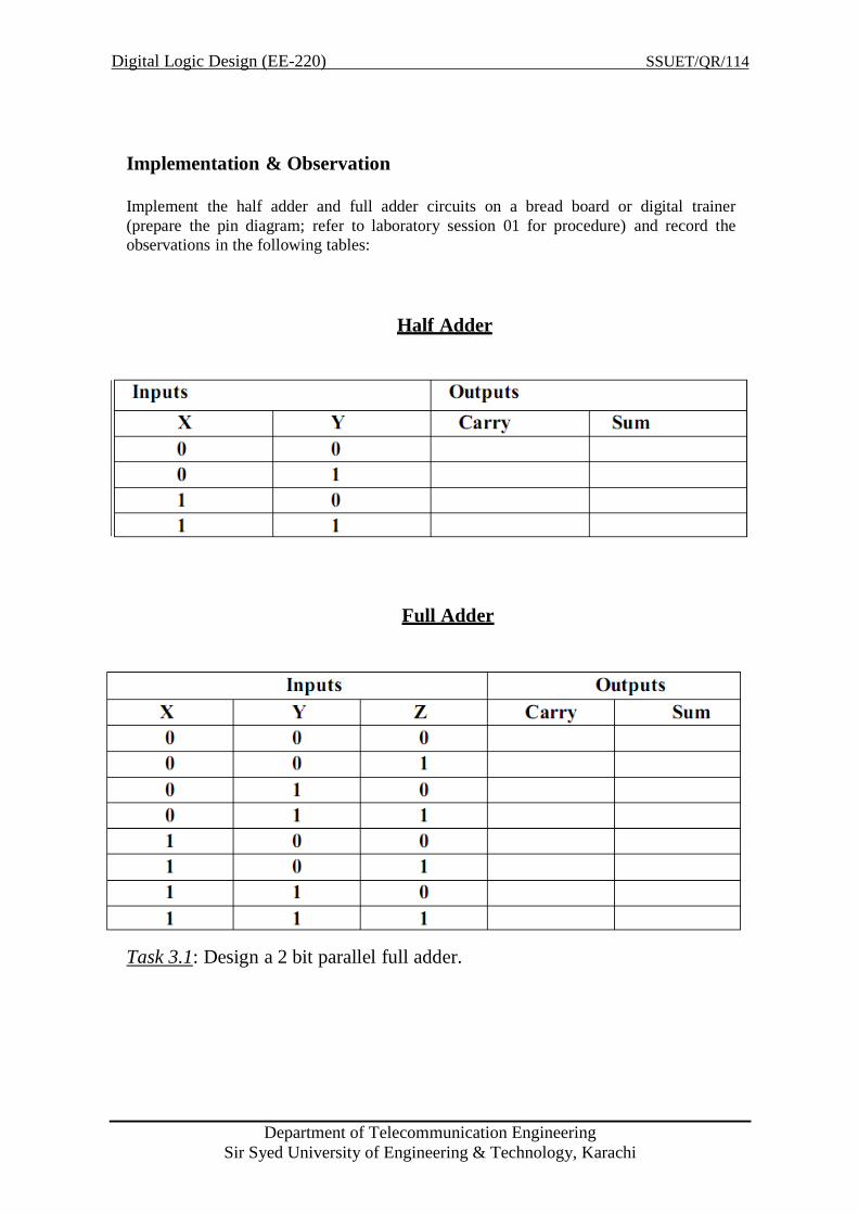
Implementation & Observation
Implement the half adder and full adder circuits on a bread board or digital trainer
(prepare the pin diagram; refer to laboratory session 01 for procedure) and record the
observations in the following tables:
Half Adder
Inputs Outputs
X Y Carry Sum
0 0
0 1
1 0
1 1
Full Adder
Inputs Outputs
X Y Z Carry Sum
0 0 0
0 0 1
0 1 0
0 1 1
1 0 0
1 0 1
1 1 0
1 1 1
Task 3.1: Design a 2 bit parallel full adder.

4SSUET/QR/11 220)-igital Logic Design (EED
Department of Telecommunication Engineering
Sir Syed University of Engineering & Technology, Karachi
Experiment No 4
Objective Implementation of 4 variable Karnaugh-Map (SOP).
Given Logic Expression
F (A, B, C, D) = ∑ (0, 1, 2, 4, 5, 6, 8, 9, 12, 13, 14)
Components and Apparatus Required
Bread board
5 V – Power supply
Multimeter.
logic probe
LEDs with resistors.
Connecting wires.
Following Digital ICs and their Datasheets
7408 Quad 2-input AND Gate
7432 Quad 2-input OR Gate
7404 Hex Inverter
Procedure 1. Construct the truth table of given logic expression.
2. Use Karnaugh- map to reduce the given function.
3. Draw the circuit diagram for the obtained reduced function.
4. Implement the reduced circuit using digital ICs on a bread board.
5. Observe the output and record it in the observation table and check it with the truth table.

4SSUET/QR/11 220)-igital Logic Design (EED
Department of Telecommunication Engineering
Sir Syed University of Engineering & Technology, Karachi
Reduction Of Logic Of Expression Using Karnaugh Map
__
C D C D C D C D
A B
A B
A B
A B
Logic Diagram (Reduced Form)
Result
The reduced form (SOP Expression) of the given logic function is:

4SSUET/QR/11 220)-igital Logic Design (EED
Department of Telecommunication Engineering
Sir Syed University of Engineering & Technology, Karachi
Constructed Truth Table
Task 4.1: Use the Karnaugh Map (POS Expression) to reduce the
logical expression
F (A, B, C, D) = Π (0, 1, 2, 4, 5, 6, 8, 9, 12, 13, 14)
Task Result:
The reduced form (POS Expression) of the given logic function is:
4SSUET/QR/11 220)-igital Logic Design (EED
Department of Telecommunication Engineering
Sir Syed University of Engineering & Technology, Karachi
Experiment No. 5 (a)
Objective To convert given binary numbers to gray codes
Components & Apparatus Required Bread board/Digital Trainer
5V power supply
Multimeter/ Logic probe
LEDs with Resistors
IC 7486
Connecting wires
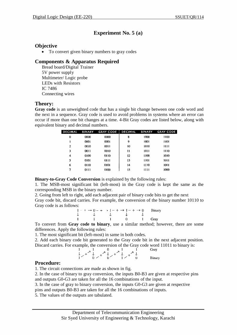
Theory: Gray code is an unweighted code that has a single bit change between one code word and
the next in a sequence. Gray code is used to avoid problems in systems where an error can
occur if more than one bit changes at a time. 4-Bit Gray codes are listed below, along with
equivalent binary and decimal numbers.
Binary-to-Gray Code Conversion is explained by the following rules:
1. The MSB-most significant bit (left-most) in the Gray code is kept the same as the
corresponding MSB in the binary number.
2. Going from left to right, add each adjacent pair of binary code bits to get the next
Gray code bit, discard carries. For example, the conversion of the binary number 10110 to
Gray code is as follows:
To convert from Gray code to binary, use a similar method; however, there are some
differences. Apply the following rules:
1. The most significant bit (left-most) in same in both codes.
2. Add each binary code bit generated to the Gray code bit in the next adjacent position.
Discard carries. For example, the conversion of the Gray code word 11011 to binary is:
Procedure: 1. The circuit connections are made as shown in fig.
2. In the case of binary to gray conversion, the inputs B0-B3 are given at respective pins
and outputs G0-G3 are taken for all the 16 combinations of the input.
3. In the case of gray to binary conversion, the inputs G0-G3 are given at respective
pins and outputs B0-B3 are taken for all the 16 combinations of inputs.
5. The values of the outputs are tabulated.
4SSUET/QR/11 220)-igital Logic Design (EED
Department of Telecommunication Engineering
Sir Syed University of Engineering & Technology, Karachi
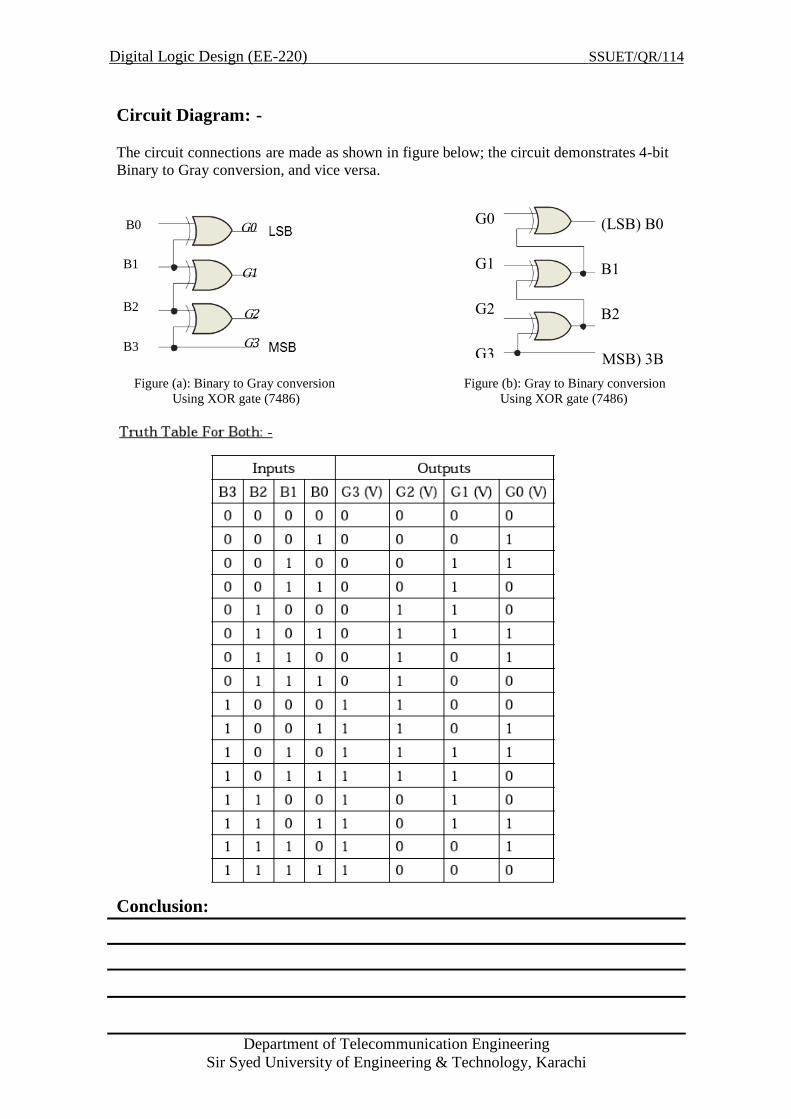
Circuit Diagram: -
The circuit connections are made as shown in figure below; the circuit demonstrates 4-bit
Binary to Gray conversion, and vice versa. B0
B1
B2
B3
Figure (a): Binary to Gray conversion Figure (b): Gray to Binary conversion
Using XOR gate (7486) Using XOR gate (7486)
Conclusion:
0G
1G
2G
3G
GG
GG
GG
GG
0B LB LG
GL
GL
B LB GL
4SSUET/QR/11 220)-igital Logic Design (EED
Department of Telecommunication Engineering
Sir Syed University of Engineering & Technology, Karachi
Experiment No. 5 (b)
Objective Designing an Odd Parity Generator and Checker for a 3-bit Data
Components & Apparatus Required Bread board/Digital Trainer
5 V - Power Supply
Multimeter
Logic Probe
LEDs with Resistors
Connecting wires
Following ICs and their Datasheets: 7486 Quad 2-mput Exclusive-OR Gates
7404 Hex Inverter
Theory
Parity Generator When binary data is transmitted and processed (like all electrical signals, it is also
susceptible to noise and contents can be altered or distorted), it may be effectively changed
from 1s to 0s and vice versa. To overcome this problem one or more bits are often added
to data as an aid in detecting errors caused by noise. The most common of these is a
parity bit that signifies whether the total number of 1s in a code group is odd or even.
In an odd parity system the parity bit is made 0 or 1 as necessary to make the total number
1s odd. Table 6.1 shows how parity bits would be added to BCD code group in both systems.
Parity Bit BCD Value
Decimal
Odd parity Even parity
1 0 0000 0 0 1 0001 1 0 1 0010 2
1 0 0011 3 0 1 0100 4
1 0 0101 5
1 0 0110 6
0 1 0111 7
0 1 1000 8
1 0 1001 9
Table 1: Odd and Even Parity in BCD
When digital data is received, a parity checking circuit generates an error signal if the
total number of 1s odd in an even parity system or if it is even in an odd parity system.
Parity check always detects a single error (one bit change from 0 to 1 or 1 to 0) but may
not detect two or more errors. Odd parity is used more often than even parity because
even parity does not detect a situation where all 0s are created due to short circuit or
other fault condition.
4SSUET/QR/11 220)-igital Logic Design (EED
Department of Telecommunication Engineering
Sir Syed University of Engineering & Technology, Karachi
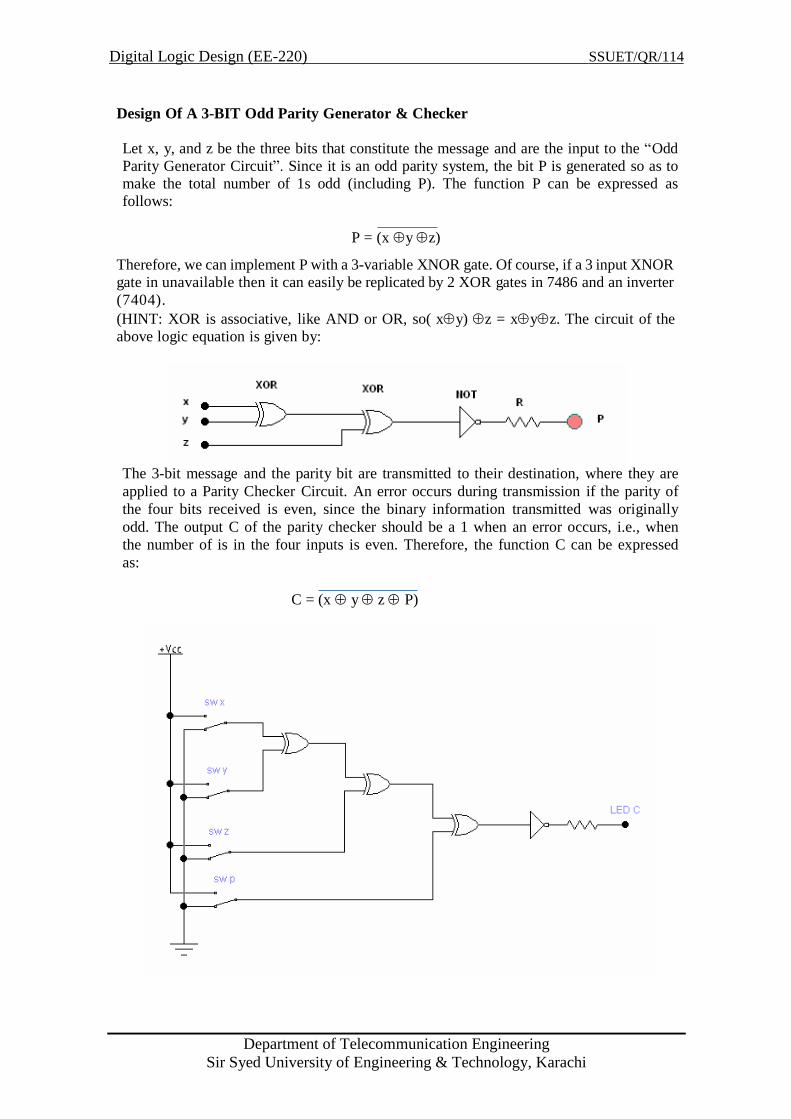
Design Of A 3-BIT Odd Parity Generator & Checker
Let x, y, and z be the three bits that constitute the message and are the input to the “Odd
Parity Generator Circuit”. Since it is an odd parity system, the bit P is generated so as to
make the total number of 1s odd (including P). The function P can be expressed as
follows:
P = (x y z)
Therefore, we can implement P with a 3-variable XNOR gate. Of course, if a 3 input XNOR
gate in unavailable then it can easily be replicated by 2 XOR gates in 7486 and an inverter
(7404).
(HINT: XOR is associative, like AND or OR, so( xy) z = xyz. The circuit of the
above logic equation is given by:
The 3-bit message and the parity bit are transmitted to their destination, where they are
applied to a Parity Checker Circuit. An error occurs during transmission if the parity of
the four bits received is even, since the binary information transmitted was originally
odd. The output C of the parity checker should be a 1 when an error occurs, i.e., when
the number of is in the four inputs is even. Therefore, the function C can be expressed
as:
C = (x y z P)
4SSUET/QR/11 220)-igital Logic Design (EED
Department of Telecommunication Engineering
Sir Syed University of Engineering & Technology, Karachi
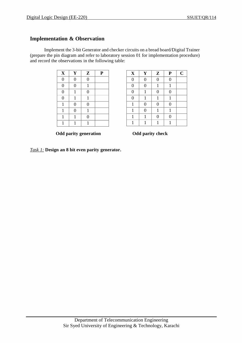
Implementation & Observation
Implement the 3-bit Generator and checker circuits on a bread board/Digital Trainer
(prepare the pin diagram and refer to laboratory session 01 for implementation procedure)
and record the observations in the following table:
Odd parity generation Odd parity check
Task 1: Design an 8 bit even parity generator.
P Z Y X
0 0 0
1 0 0
0 1 0
1 1 0
0 0 1
1 0 1
0 1 1
1 1 1
C P Z Y X
0 0 0 0
1 1 0 0
0 0 1 0
1 1 1 0
0 0 0 1
1 1 0 1
0 0 1 1
1 1 1 1
4SSUET/QR/11 220)-igital Logic Design (EED
Department of Telecommunication Engineering
Sir Syed University of Engineering & Technology, Karachi
Experiment No. 6
Objective Designing of a 4x2 Priority Encoder
Experimenting with 74148IC Octal (8x3) Priority Encoder.
Components & Apparatus Required Bread board/Digital Trainer
5v power supply
Multimeter
Logic probe
LEDs with Resistors
Connecting wires,
Following ICs and their Datasheets:
74148 8 x 3 octal priority encoder
7408 Quad 2-input or 7421 Dual 4-input AND Gates
7432 Quad 2-input OR Gates
7404 Hex Inverter.
Theory
Encoder An encoder is a digital function that produces a reverse operation from that of a decoder. An
Encoder has 2n
(or less) inputs lines and n output lines. The output lines generate the binary
code for the 2n
inputs variables.
Priority Encoder A simple encoder may produce an erroneous output if more than one of its inputs is high. A
Priority Encoder is one that responds to just one input among those that may be
simultaneously high, in accordance with some priority system. The most common priority system
is based on the relative magnitudes of the inputs: whichever decimal input is largest, is the one
that is encoded.
Design of a 4 X 2 Priority Encoder
The following equations represent the outputs of a 4 x 2 priority encoder:
A = D2 + D3
_
B = D1D2 + D3
As can be seen from the equations that input D0, which has a binary code 00, is not used
in any equation. A binary code 00 at the output indicates two conditions: Either D0 is selected
or no input is selected. In order to differentiate these two conditions, we will provide an additional
output, Z to indicate if at least one of the inputs is a 1. The equation for Z will be:
4SSUET/QR/11 220)-igital Logic Design (EED
Department of Telecommunication Engineering
Sir Syed University of Engineering & Technology, Karachi
Z = D0 + D2 + D3 + D4
If Z is 1, then the binary code 00 at the output indicates that D0 is selected and if Z is 0, then it
indicates that no input line is selected.
Logic Implementation:
Figure 6.1

4SSUET/QR/11 220)-igital Logic Design (EED
Department of Telecommunication Engineering
Sir Syed University of Engineering & Technology, Karachi
Implementation & Observations Implement the 4 x 2 priority encoder circuit figure 6.1 on bread board (prepare the pin diagram;
refer to laboratory session #01 for implementation procedure) and record the observation in the
following table:
D3 D2 D1 D0 Expected Observed
A B Z A B Z
0 0 0 0 0 0 0 0 0 0 1 0 0 1 0 0 1 X 0 1 1 0 1 X X 1 0 1 1 X X X 1 1 1
Task 6.1: Design a 4x2 Priority encoder having priority system based on the relative
magnitudes of the inputs: whichever decimal input is smallest is the one that is encoded.
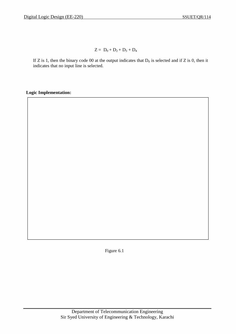
Task 6.2: Testing of 74148 8 x 3 octal priority Encoder
The 74148 is a priority encoder with active-Low input for decimal digits. There are nine inputs
lines (including an enable input) and five output lines, of which three represents the binary code
for the octal digit. Function of various pins of this IC is described below:
1. 0 through 7: Active low data inputs representing the octal digits.
2. A2, A1, A0: Active low output lines representing the binary code
3.El: Active low enable Input . 4.EO: Active low output indicating none of the inputs is high
5.GS: Active low output indicating any of the inputs is high
6.VCC and GND: Supply connections; lines
Therefore if GS, A2, Al, and A0 are all low, then it shows that line 0 is selected and if EO, A2, Al,
and AO are all low then it shows that none of the inputs selected. EO and GS cannot be in the
same state provided that El is enabled.
4SSUET/QR/11 220)-igital Logic Design (EED
Department of Telecommunication Engineering
Sir Syed University of Engineering & Technology, Karachi
Pin Configuration:
Figure 6.2: Pins of 74148
Testing Procedure Make connections according to the above explanation.
Apply different combinations of 1s and 0s at data inputs.
Observe the output and record your observations in the following table.
Observation
Inputs Expected Output Values Observed Output
E1 0 1 2 3 4 5 6 7 A2 A1 A0 GS E0 A2 A1 A0 GS E0
1 X X X X X X X X 0 0 0 0 0
0 1 1 1 1 1 1 1 1 0 0 0 1 0
0 X X X X X X X 0 0 0 0 0 1
0 X X X X X X 0 1 0 0 1 0 1
0 X X X X X 0 1 1 0 1 0 0 1
0 X X X X 0 1 1 1 0 1 1 0 1
0 X X X 0 1 1 1 1 1 0 0 0 1
0 X X 0 1 1 1 1 1 1 0 1 0 1
0 X 0 1 1 1 1 1 1 1 1 0 0 1
0 0 1 1 1 1 1 1 1 1 1 1 0 1

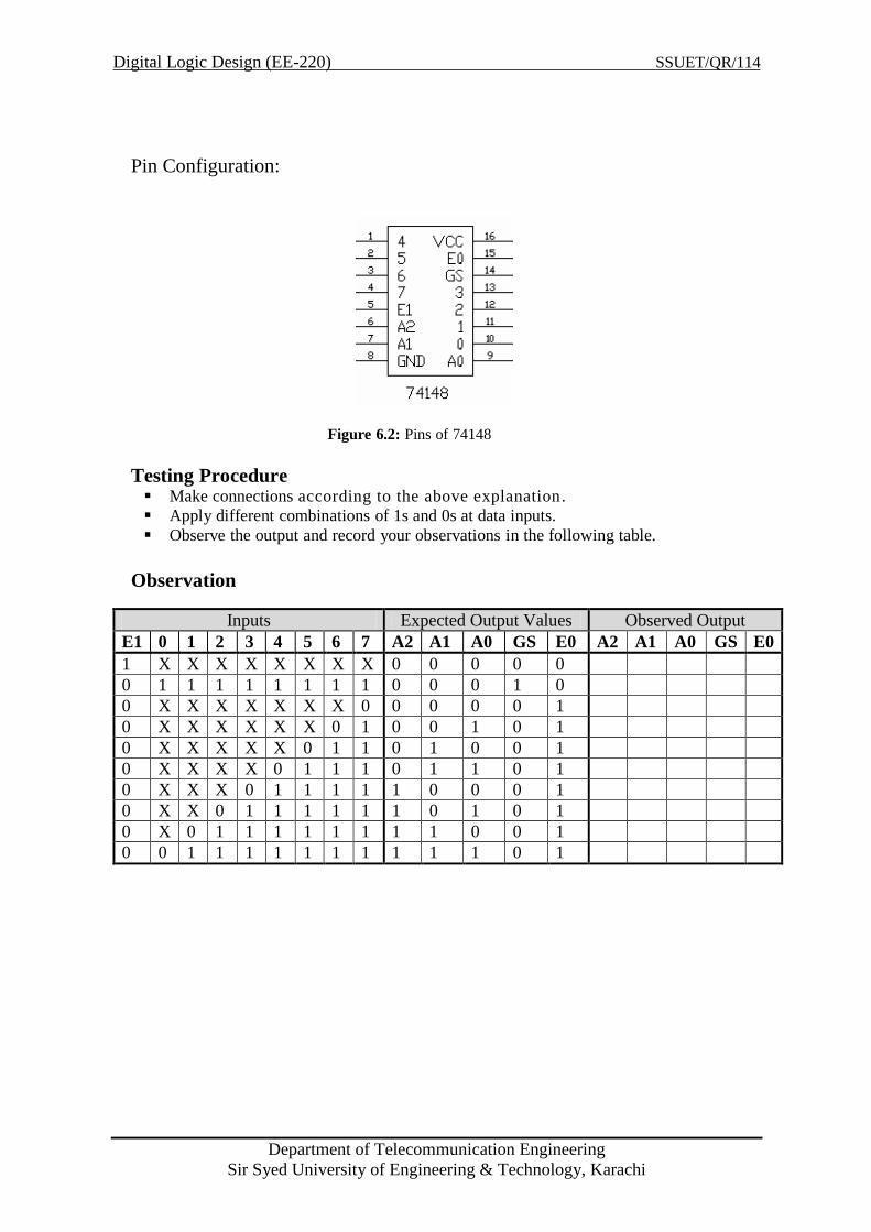
Experiment No. 7
Objective Designing of a 2x4 Decoder / 1x4 De-multiplexer Experimenting with 74138IC.
Components & Apparatus RequiredBread board/Digital Trainer5 V - Power SupplyMultimeterLogic ProbeLEDs with ResistorsConnecting Wires
Following ICs and their Datasheets .7408 Quad 2-input or 7411 Triple 3-input AND Gates7404 Hex Inverter74138 3x8 Decoder
Theory
DecoderA Decoder is a combinational circuit that converts binary information from 'n' input lines to amaximum of 2 n unique output lines. In practical applications, decoders are often used forselecting one of several devices.
A decoder with an enable input can function as a Demultiplexer. A Demultiplexer (DMUX)is a circuit that receives information on a single line and transmits this information on one of2n possible output lines. The selection of a specific output line is controlled by the bit valuesof 'n' selection lines.
Design Of 2 x 4 Decoder / 1 x 4 De-multiplexerA 2 x 4 decoder is capable of selecting one of four output lines (see figure 1 (a)). The 2-bit binary numbers at the data inputs, Si and So, specifies which of the four data inputsis to be selected. If we add an enable pin and use it as an input line, then this decodercan be converted to a 1 x 4 Demultiplexer, where Si arid So will select a line to whichdata input is to be routed (see figure 1 (b)).
De-Multiplexer

Inputs SelectInputs
Enable DataInput
Fig 1(a) Fig 1(b)
Figure 2: Circuit Diagram for 2 x 4 Decoder/ 1 x 4 Demultiplexer
SoS1
D0
D1
D3
D4
D-out
D-in
SoS1
SoS1

Implementation & ObservationsImplement the 2x4 Decoder /1 x 4 De multiplexer circuit (figure 2) on a bread board (preparethe pin diagram by referring to laboratory session 1 for implementation procedure) and recordthe observations in the following table.
Enable / Data Input S1 So Do D1 D2 D3
0 0 00 0 10 1 00 1 11 0 01 0 11 1 01 1 1
Testing Of 74138 3 x 8 DecoderThe 74138 IC has three inputs and eight output lines. It has three enable inputs and for IC tofunction all three inputs need to be enabled. Function of various pins of this IC is describedbelow
1. YO through Y7: Active low data outputs2. A, B, C: Input / select lines with C being the MSB3. Gl: Active high enable Input4. G2A' and G2B': Active low enable Inputs5. VCC and GND: Supply connections line
Circuit Diagram
Testing Procedure
1. Make connections as shown in the circuit diagram.2. Apply different combinations of Is and 0s at data inputs3. Observe the output and record your observations in the following table.
Observation
C B A Y0 Y1 Y2 Y3 Y4 Y5 Y6 Y70 0 00 0 10 1 00 1 11 0 01 0 11 1 01 1 1
Task 1: Design 1x4 Demultiplexer using logic gates.

Experiment No. 8
Objective Designing of a 4x1 Multiplexer Experimenting with 74151 IC.
Components & Apparatus Required1. Following ICs and their Datasheets:
I. 7411 Triple 3-input AND Gates.II. 7432 Quad 2-input OR Gates.
III. 7404 Hex Inverter.IV. 74151 8 x 1 MUX
2. Bread board/Digital Trainer.3. 5V power supply.4. Multimeter.5. Logic Probe.6. LEDs with Resistors7. Connecting wires.
Theory
MultiplexersA digital data Multiplexer (MUX) is a combinational circuit having several data inputsand a single output. A set of data-select inputs is used to control when of the data an inputis routed to the single output. A multiplexer is also called a data selector because of thisability to select which data input is connected to the output. Normally there are 2n inputlines and n selection lines whose bit combination determine which input is selected.
Design Of 4 x 1 MultiplexerA 4 x 1 multiplexer is capable of selecting one of four data inputs (see figure 1). The 2-bit binary number at the data select inputs, Si and So, specifies which of the four datainputs is to be routed to the output. Since there are two data select inputs, therefore theycan select 22 = 4 different data inputs lines.
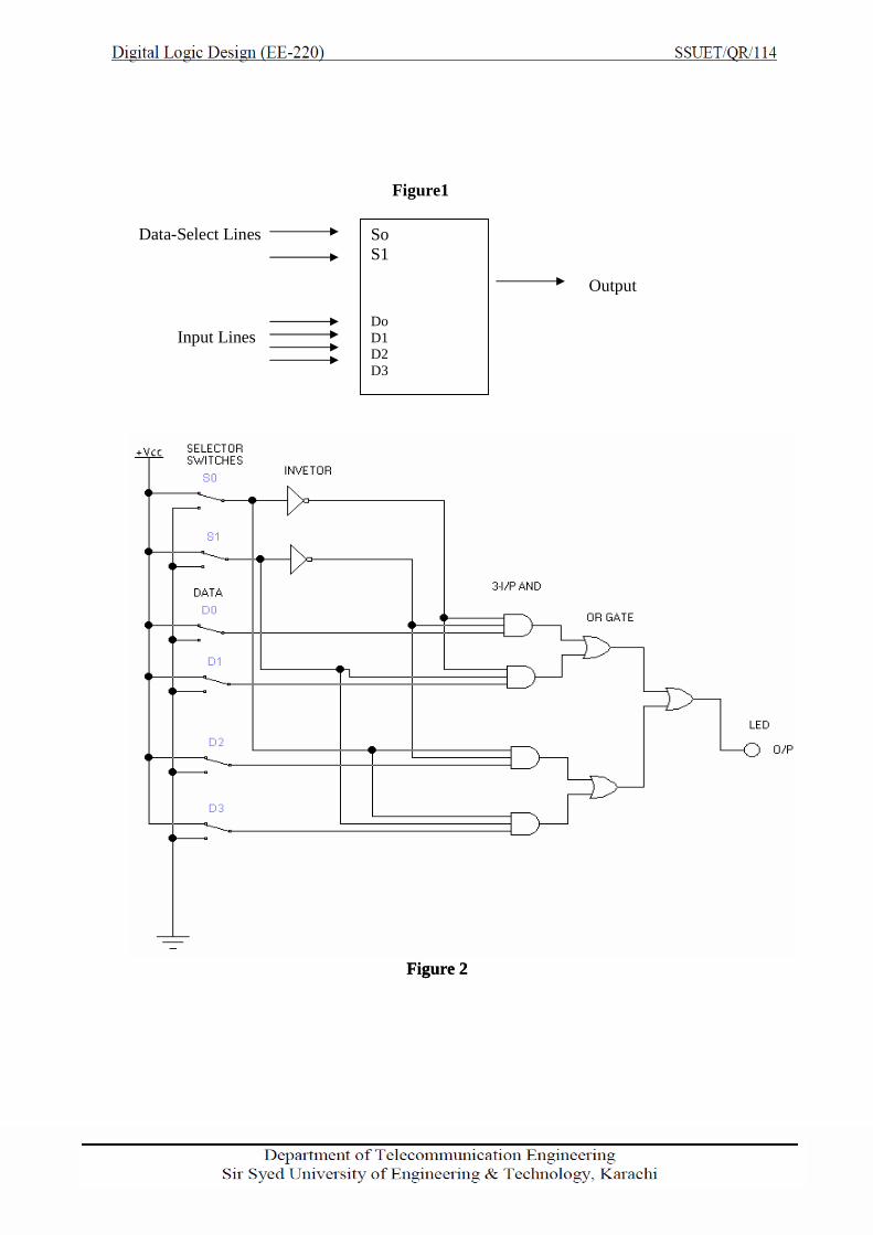
Figure 2
Output
SoS1
DoD1D2D3
Data-Select Lines
Input Lines
Figure 2
Figure1

ProcedureImplement the 4x1 Multiplexer circuit on a bread board/Digital Trainer as shown infigure 2; prepare the pin diagram (by referring to laboratory session 01 forimplementation procedure for NOT, AND and OR gates) and record the observations inthe following, table. For each data select combination, specify the switch number as wellas the binary value present on that selected switch.
Observation
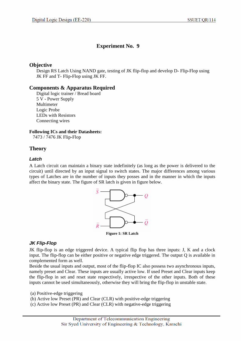
Task 1: TESTING OF 74151A -8 x 1 MUXThe 74151A IC has eight data inputs and three data-selection lines. Function of variouspins of this IC is described below:1. D0 through D7: Data input lines2. A, B, C, : Data select lines with C being the MSB3. Y: Output line.4. W: Inverted output line.5. G': Active low enable line6. VCC and GND: Supply connections linesTesting Procedure1. Make connections as shown in the figure 3 on bread board/Digital Trainer.2. Select the data input D0 (applied both 0 & 1) with the help of data selectors A, B, andC.3. Apply different data (1 or 0) at data inputs that are labeled as D0 to D7.4. Observe the output, which shows the data from D0.5. Select all the eight data inputs one by one and record your observations in thefollowing table.
D3 D2 D1 D0 S1 So OUTPUT0 1 0 1 0 0
0 1 0 1 0 1
0 1 0 1 1 0
0 1 0 1 1 1
1 0 1 0 0 0
1 0 1 0 0 1
1 0 1 0 1 0
1 0 1 0 1 1
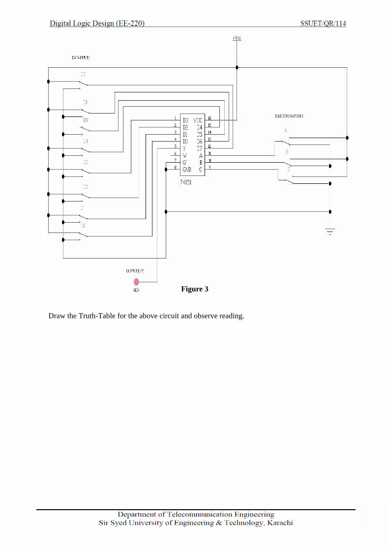
Figure 3
Draw the Truth-Table for the above circuit and observe reading.
Experiment No. 9
ObjectiveDesign RS Latch Using NAND gate, testing of JK flip-flop and develop D- Flip-Flop usingJK FF and T- Flip-Flop using JK FF.
Components & Apparatus RequiredDigital logic trainer / Bread board5 V - Power SupplyMultimeterLogic ProbeLEDs with ResistorsConnecting wires
Following ICs and their Datasheets:7473 / 7476 JK Flip-Flop
Theory
Latch
A Latch circuit can maintain a binary state indefinitely (as long as the power is delivered to thecircuit) until directed by an input signal to switch states. The major differences among varioustypes of Latches are in the number of inputs they posses and in the manner in which the inputsaffect the binary state. The figure of SR latch is given in figure below.
Figure 1: SR Latch
JK Flip-Flop
JK flip-flop is an edge triggered device. A typical flip flop has three inputs: J, K and a clockinput. The flip-flop can be either positive or negative edge triggered. The output Q is available incomplemented form as well.Beside the usual inputs and output, most of the flip-flop IC also possess two asynchronous inputs,namely preset and Clear. These inputs are usually active low. If used Preset and Clear inputs keepthe flip-flop in set and reset state respectively, irrespective of the other inputs. Both of theseinputs cannot be used simultaneously, otherwise they will bring the flip-flop in unstable state.
(a) Positive-edge triggering(b) Active low Preset (PR) and Clear (CLR) with positive-edge triggering(c) Active low Preset (PR) and Clear (CLR) with negative-edge triggering
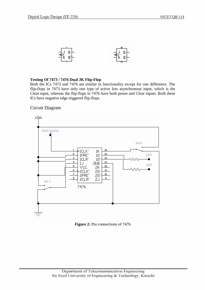
Testing Of 7473 / 7476 Dual JK Flip-FlopBoth the ICs 7473 and 7476 are similar in functionality except for one difference. Theflip-flops in 7473 have only one type of active low asynchronous input, which is theClear input, whereas the flip-flops in 7476 have both preset and Clear inputs. Both theseICs have negative edge triggered flip-flops.
Circuit Diagram
Figure 2: Pin connections of 7476

Testing Procedure1. Make connections as shown in the diagram (Figure 1 and Figure 2).2. Apply different combinations of 1s and 0s at S and R inputs3. Apply different combinations of 1s and 0s at J and K inputs4. Observe the output and record your observations in the following table.
Observations
S R Q0 00 11 01 1
J K Q0 00 11 01 1
Task 12.1: Design a D-Flip Flop using JK-Flip Flop.
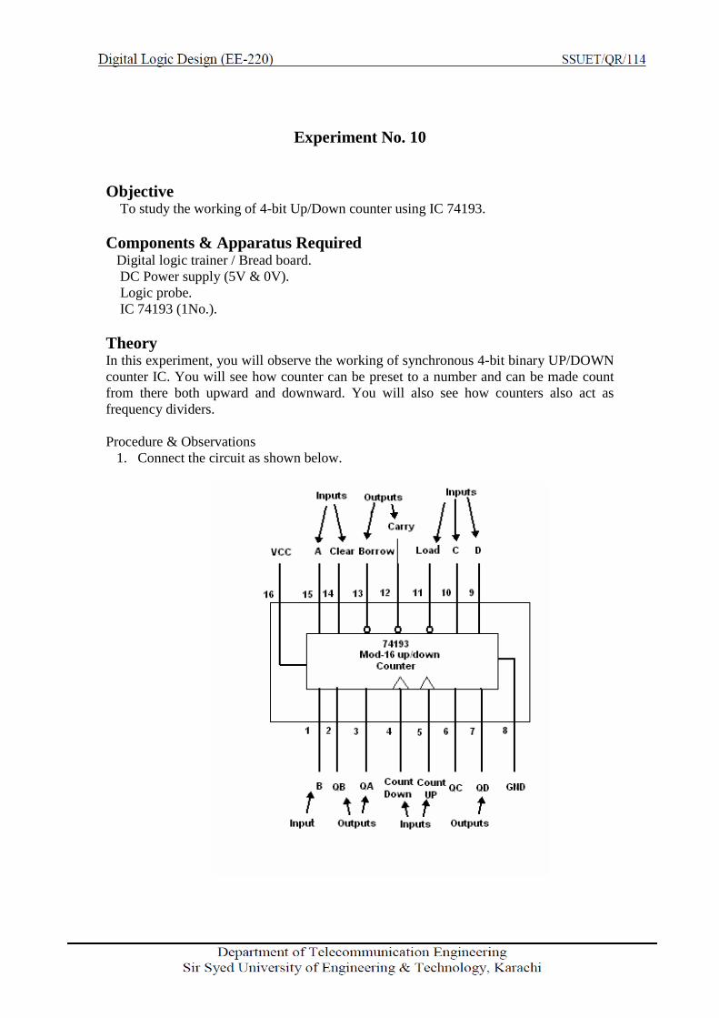
Experiment No. 10
ObjectiveTo study the working of 4-bit Up/Down counter using IC 74193.
Components & Apparatus RequiredDigital logic trainer / Bread board.DC Power supply (5V & 0V).Logic probe.IC 74193 (1No.).
TheoryIn this experiment, you will observe the working of synchronous 4-bit binary UP/DOWNcounter IC. You will see how counter can be preset to a number and can be made countfrom there both upward and downward. You will also see how counters also act asfrequency dividers.
Procedure & Observations1. Connect the circuit as shown below.

2. Connect the clear input (pin#14) to logic High and observe the outputs of counter(pin#7,6,2,3) by connecting them to Logic probe (or LEDs).
QD, QC, QB, QA = ____________________
Connect pin#14 back to logic low.3. Connect the data inputs (D, C, B, A i.e. pin#9, 10, 1, 15) to logic 0110.4. Now, activate the LOAD input (pin#11) by connecting it to logic Low (0V).
What do you observe at the outputs (pin#7,6,2,3).
QD, QC, QB, QA = ____________________
You will see that the counter will be preset to the data loaded into it (0110).Connect Load input back to logic High (5V).
5. At the count UP clock input (pin#5) connect the pulse-wave output of frequency 1Hz.
Now what do you observe?
6. Observe the output at carry (pin#12). How will you relate this output to the fouroutputs QD, QC, QB, QA?
7. Now change the pulse-wave output of frequency 1 Hz from the count UP clockinput (pin#5) to the count DOWN clock input (pin#4).
What do you observe at the outputs?

8. Observe the output at Borrow (pin#13). How will you relate this output to the fouroutputs QD, QC, QB, QA?
9. Now set the square-wave generator frequency at 10 KHz and voltage at 5V thenconnect its output to pin#4. Observe the signal at pin#4 and pin#13 on oscilloscopeCh-1 & 2 and measure the frequency of both outputs.
Fclk = _____________ fBorrow = ____________
How will you relate the two?
Experiment No. 11
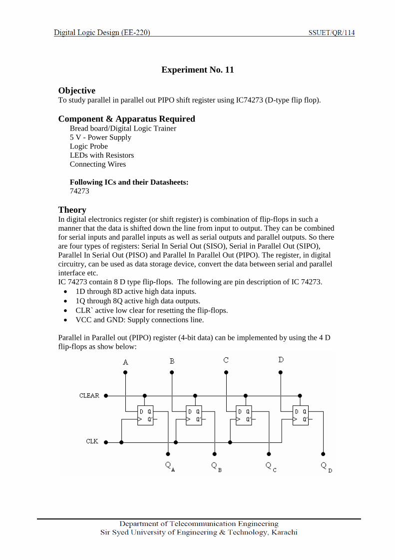
ObjectiveTo study parallel in parallel out PIPO shift register using IC74273 (D-type flip flop).
Component & Apparatus RequiredBread board/Digital Logic Trainer5 V - Power SupplyLogic ProbeLEDs with ResistorsConnecting Wires
Following ICs and their Datasheets:74273
TheoryIn digital electronics register (or shift register) is combination of flip-flops in such amanner that the data is shifted down the line from input to output. They can be combinedfor serial inputs and parallel inputs as well as serial outputs and parallel outputs. So thereare four types of registers: Serial In Serial Out (SISO), Serial in Parallel Out (SIPO),Parallel In Serial Out (PISO) and Parallel In Parallel Out (PIPO). The register, in digitalcircuitry, can be used as data storage device, convert the data between serial and parallelinterface etc.IC 74273 contain 8 D type flip-flops. The following are pin description of IC 74273. 1D through 8D active high data inputs. 1Q through 8Q active high data outputs. CLR` active low clear for resetting the flip-flops. VCC and GND: Supply connections line.
Parallel in Parallel out (PIPO) register (4-bit data) can be implemented by using the 4 Dflip-flops as show below:
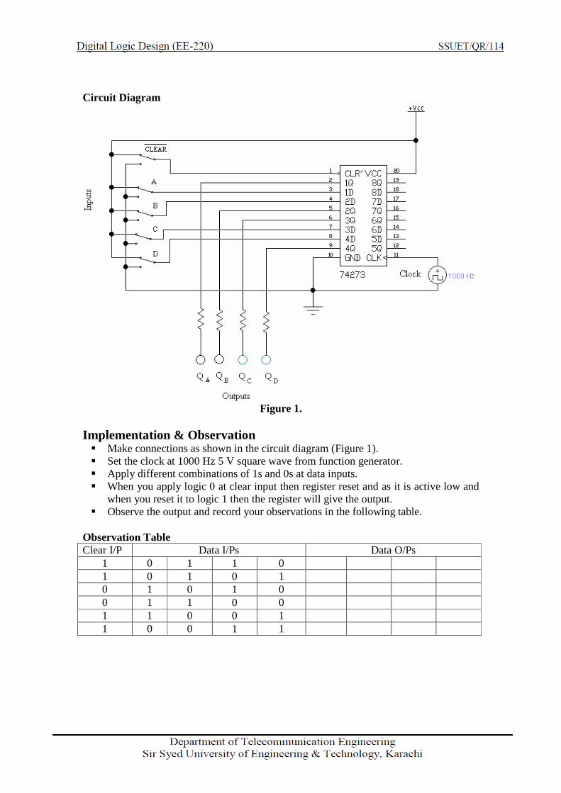
Circuit Diagram
Figure 1.
Implementation & Observation Make connections as shown in the circuit diagram (Figure 1). Set the clock at 1000 Hz 5 V square wave from function generator. Apply different combinations of 1s and 0s at data inputs. When you apply logic 0 at clear input then register reset and as it is active low and
when you reset it to logic 1 then the register will give the output. Observe the output and record your observations in the following table.
Observation TableClear I/P Data I/Ps Data O/Ps
1 0 1 1 01 0 1 0 10 1 0 1 00 1 1 0 01 1 0 0 11 0 0 1 1

Experiment No. 12
ObjectiveDesign Serial in Serial out shift register using JK FF and implement it using 74273 IC.
Component & Apparatus RequiredBread board/Digital Logic Trainer5 V - Power SupplyLogic ProbeLEDs with ResistorsConnecting Wires
Following ICs and their Datasheets:74273
TheoryIn digital electronics register (or shift register) is combination of flip-flops in such amanner that the data is shifted down the line from input to output. They can be combinedfor serial inputs and parallel inputs as well as serial outputs and parallel outputs. So thereare four types of registers: Serial In Serial Out (SISO), Serial in Parallel Out (SIPO),Parallel In Serial Out (PISO) and Parallel In Parallel Out (PIPO). The register, in digitalcircuitry, can be used as data storage device, convert the data between serial and parallelinterface etc.IC 74273 contains 8 D type flip-flops. The following are pin description of IC 74273. 1D through 8D active high data inputs. 1Q through 8Q active high data outputs. CLR active low clear for resetting the flip-flops. VCC and GND: Supply connections line.
Serial in Serial out (SISO) register (4-bit data) can be implemented by using the 4 D flip-flops as show below:
Figure 1

Figure 2.
Implementation & Observation Make connections using figure 1 and figure 2. Set the clock at 1000 Hz 5 V square wave from function generator. Apply different combinations of 1s and 0s at data inputs. When you apply logic 0 at clear input then register reset and as it is active low and
when you reset it to logic 1 then the register will give the output. Observe the output and record your observations in the following table.
Observation Table
Clear I/P Data I/Ps Data O/Ps0 11 01 11 01 01 1
-
_____________________________________________________________________________________
Department of Telecommunication Engineering
Sir Syed University of Engineering & Technology, Karachi
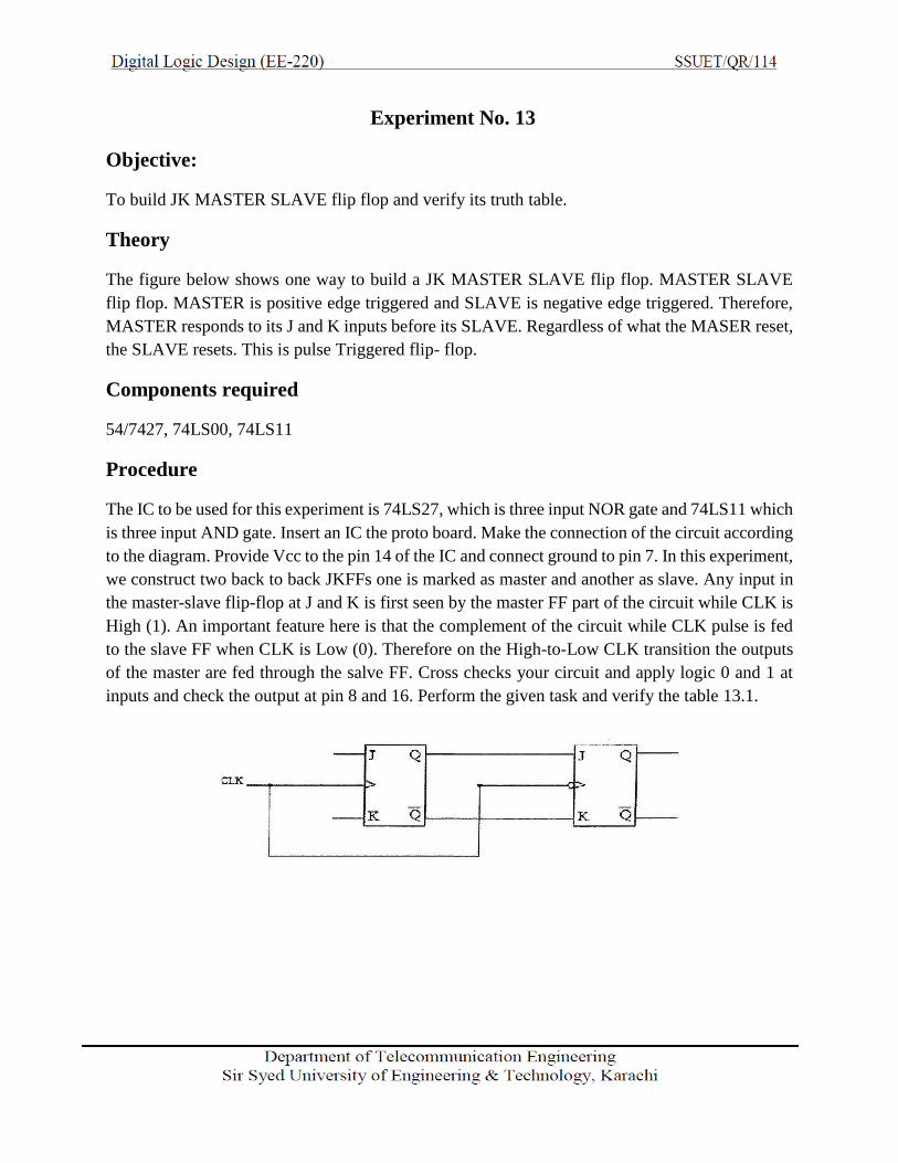
Experiment No. 13
Objective:
To build JK MASTER SLAVE flip flop and verify its truth table.
Theory
The figure below shows one way to build a JK MASTER SLAVE flip flop. MASTER SLAVE
flip flop. MASTER is positive edge triggered and SLAVE is negative edge triggered. Therefore,
MASTER responds to its J and K inputs before its SLAVE. Regardless of what the MASER reset,
the SLAVE resets. This is pulse Triggered flip- flop.
Components required
54/7427, 74LS00, 74LS11
Procedure
The IC to be used for this experiment is 74LS27, which is three input NOR gate and 74LS11 which
is three input AND gate. Insert an IC the proto board. Make the connection of the circuit according
to the diagram. Provide Vcc to the pin 14 of the IC and connect ground to pin 7. In this experiment,
we construct two back to back JKFFs one is marked as master and another as slave. Any input in
the master-slave flip-flop at J and K is first seen by the master FF part of the circuit while CLK is
High (1). An important feature here is that the complement of the circuit while CLK pulse is fed
to the slave FF when CLK is Low (0). Therefore on the High-to-Low CLK transition the outputs
of the master are fed through the salve FF. Cross checks your circuit and apply logic 0 and 1 at
inputs and check the output at pin 8 and 16. Perform the given task and verify the table 13.1.
-220)
_____________________________________________________________________________________
Department of Telecommunication Engineering
Sir Syed University of Engineering & Technology, Karachi
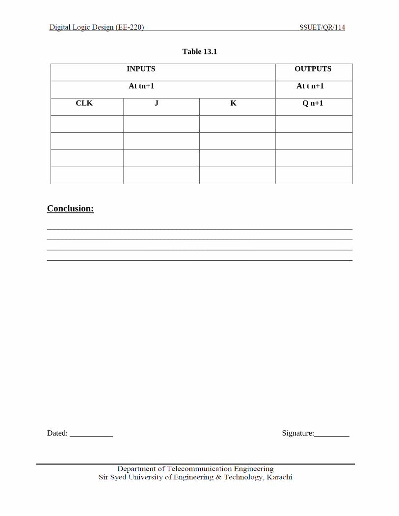
Table 13.1
INPUTS OUTPUTS
At tn+1 At t n+1
CLK J K Q n+1
Conclusion:
______________________________________________________________________________
______________________________________________________________________________
______________________________________________________________________________
______________________________________________________________________________
Dated: ___________ Signature:_________
-220)
_____________________________________________________________________________________
Department of Telecommunication Engineering
Sir Syed University of Engineering & Technology, Karachi
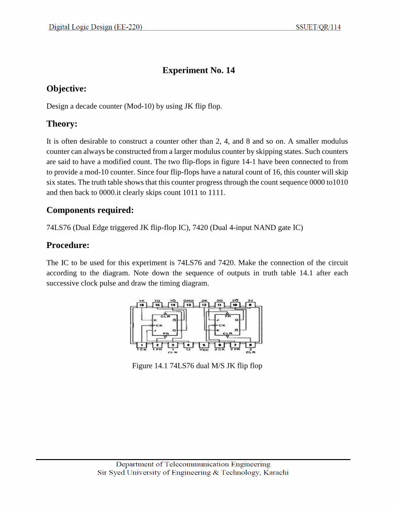
Experiment No. 14
Objective:
Design a decade counter (Mod-10) by using JK flip flop.
Theory:
It is often desirable to construct a counter other than 2, 4, and 8 and so on. A smaller modulus
counter can always be constructed from a larger modulus counter by skipping states. Such counters
are said to have a modified count. The two flip-flops in figure 14-1 have been connected to from
to provide a mod-10 counter. Since four flip-flops have a natural count of 16, this counter will skip
six states. The truth table shows that this counter progress through the count sequence 0000 to1010
and then back to 0000.it clearly skips count 1011 to 1111.
Components required:
74LS76 (Dual Edge triggered JK flip-flop IC), 7420 (Dual 4-input NAND gate IC)
Procedure:
The IC to be used for this experiment is 74LS76 and 7420. Make the connection of the circuit
according to the diagram. Note down the sequence of outputs in truth table 14.1 after each
successive clock pulse and draw the timing diagram.
Figure 14.1 74LS76 dual M/S JK flip flop

-220)
_____________________________________________________________________________________
Department of Telecommunication Engineering
Sir Syed University of Engineering & Technology, Karachi
Figure 14.2 7420 dual 4 input NAND gate
Figure 14.3 Mod 10 counter by using JK flip flop

-220)
_____________________________________________________________________________________
Department of Telecommunication Engineering
Sir Syed University of Engineering & Technology, Karachi
Table 14.1: Truth Table for Mod 10 Counter
COUNT QD QC QB QA
0
1
2
3
4
5
6
7
8
9
10
11
12
13
14
15
Conclusion:
__________________________________________________________________
__________________________________________________________________
_________________________________________________________________
Date: ___________ Signature:_________
Experiment No. 15
Objective
To study the Programmable logic devices and familiarize with programmable
logic devices.
Components Required
Computer with WinCupl package
GAL 16 V8 device (PLD/ GAL)
Universal Programmer
Bread board
5 V - power supply
Multimeter
Logic probe
LEDs with resistors
Connecting wires
Switches
Theory Programmable Logic
Programmable logic, as the name implies, is a family of components that contains arrays
of logic elements (AND, OR, INVERT, LATCH, FLIP-FLOP) that may be configured
into any logical function that the user desires and the component supports. There are
several classes of programmable logic devices: ASICs, FPGAs, PLAs, PROMs, PALs,
GALs, and complex PLDs.
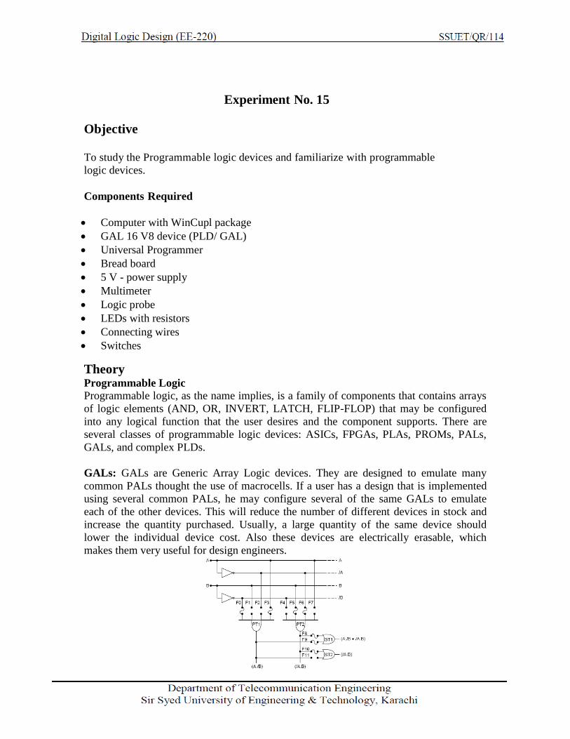
GALs: GALs are Generic Array Logic devices. They are designed to emulate many
common PALs thought the use of macrocells. If a user has a design that is implemented
using several common PALs, he may configure several of the same GALs to emulate
each of the other devices. This will reduce the number of different devices in stock and
increase the quantity purchased. Usually, a large quantity of the same device should
lower the individual device cost. Also these devices are electrically erasable, which
makes them very useful for design engineers.
Logical Operators
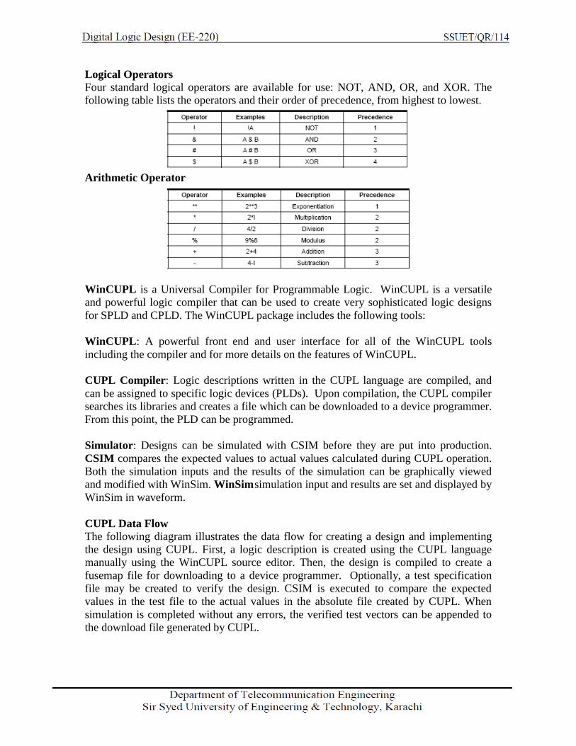
Four standard logical operators are available for use: NOT, AND, OR, and XOR. The
following table lists the operators and their order of precedence, from highest to lowest.
Arithmetic Operator
WinCUPL is a Universal Compiler for Programmable Logic. WinCUPL is a versatile
and powerful logic compiler that can be used to create very sophisticated logic designs
for SPLD and CPLD. The WinCUPL package includes the following tools:
WinCUPL: A powerful front end and user interface for all of the WinCUPL tools
including the compiler and for more details on the features of WinCUPL.
CUPL Compiler: Logic descriptions written in the CUPL language are compiled, and
can be assigned to specific logic devices (PLDs). Upon compilation, the CUPL compiler
searches its libraries and creates a file which can be downloaded to a device programmer.
From this point, the PLD can be programmed.
Simulator: Designs can be simulated with CSIM before they are put into production.
CSIM compares the expected values to actual values calculated during CUPL operation.
Both the simulation inputs and the results of the simulation can be graphically viewed
and modified with WinSim. WinSim simulation input and results are set and displayed by
WinSim in waveform.
CUPL Data Flow
The following diagram illustrates the data flow for creating a design and implementing
the design using CUPL. First, a logic description is created using the CUPL language
manually using the WinCUPL source editor. Then, the design is compiled to create a
fusemap file for downloading to a device programmer. Optionally, a test specification
file may be created to verify the design. CSIM is executed to compare the expected
values in the test file to the actual values in the absolute file created by CUPL. When
simulation is completed without any errors, the verified test vectors can be appended to
the download file generated by CUPL.
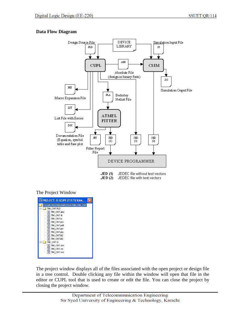
Data Flow Diagram
The Project Window
The project window displays all of the files associated with the open project or design file
in a tree control. Double clicking any file within the window will open that file in the
editor or CUPL tool that is used to create or edit the file. You can close the project by
closing the project window.

If you open a design file rather than opening it as a project, you can display the project
window at any time by choosing Project from the view menu.
The Messages Window
The messages window displays the output from the compiler consisting of both status
information and error messages generated by the compiler. If you click on an error
message, the Error Message dialog will be displayed providing more information about
the specific error.
Sample Code Name All_basic_Gates;
Partno gat110;
Revision 04;
Date IU;
Designer IU;
Company IQRA UNIVERSITY;
Location MAIN Campus;
Assembly None;
Device g16v8a;
/* Inputs Pins: define inputs and assigning the name to the input pins*/
Pin 1 = a;
Pin 2 = b;
/*Outputs Pins: define outputs as active HI levels and assigning the name to o/p pin*/
Pin 12 = nota;
Pin 13 = notb;
Pin 14 = and;
Pin 15 = nand;
Pin 16 = or;
Pin 17 = nor;
Pin 18 = xor;
Pin 19 = xnor;
/*
* Logic: Implementing logic gates
*/
nota = !a; /* inverters */
notb = !b;
and = a & b; /* and gate */
nand = !(a & b); /* nand gate */
or = a # b; /* or gate */
nor = !(a # b); /* nor gate */
xor = a $ b; /* exclusive or gate */
xnor = !(a $ b); /* exclusive nor gate */

Task 15.1: Using WinCUPL write the above code for GAL 16V8a, observe the output
and attach the simulation screen-shot.
Task 15.2: Using WinCUPL write the code for GAL 16V8a used as a Half-Adder,
observe the output and attach the simulation screen-shot.
Task 15.3: Demonstrate the working of PLD (GAL16V8) as a 4-to-1 Multiplexer. Write
the code, observe output and show simulation results as well. Compare the circuit with
the discrete component structure of the combinational logic for similar MUX.
Related Documents