1 LABORATORY MANUAL SIMULATION LABORATORY B. Tech. II/IV SEM-II, ECE Department of Electronics & Communication Engineering ANIL NEERUKONDA INSTITUTE OF TECHNOLOGY AND SCIENCES AUTONOMOUS (Affiliated to AU, Approved by AICTE &Accredited by NBA) Sangivalasa531162,Bheemunipatnam Mandal,Visakhapatnam Dt.

Welcome message from author
This document is posted to help you gain knowledge. Please leave a comment to let me know what you think about it! Share it to your friends and learn new things together.
Transcript

1
LABORATORY MANUAL
SIMULATION LABORATORY
B. Tech. II/IV SEM-II, ECE
Department of Electronics & Communication Engineering ANIL NEERUKONDA INSTITUTE OF TECHNOLOGY AND SCIENCES
AUTONOMOUS (Affiliated to AU, Approved by AICTE &Accredited by NBA)
Sangivalasa531162,Bheemunipatnam Mandal,Visakhapatnam Dt.

2
Institute Vision
ANITS envisions emerging as a world-class technical institution
whose products represent a good blend of technological
excellence and the best of human values.
Institute Mission To train young men and women into competent and confident
engineers with excellent communicational skills, to face the
challenges of future technology changes, by imparting holistic
technical education using the best of infrastructure, outstanding
technical and teaching expertise and an exemplary work culture,
besides molding them into good citizens.

3
Vision of the department
To become a centre of excellence in Education, research and
produce high quality engineers in the field of Electronics and
Communication Engineering to face the challenges of future
technology changes.
Mission of the department
The Department aims to bring out competent young Electronics
& Communication Engineers by achieving excellence in
imparting technical skills, soft skills and the right attitude for
continuous learning.

4
Programme Educational Objectives
PEO1: To prepare graduates for successful career in Electronics industries, R&D organizations and/or IT
industries by providing technical competency in the field of Electronics & Communication Engineering.
PEO2: To prepare graduates with good scientific and engineering proficiency to analyze and solve
electronic engineering problems.
PEO3: To inculcate in students professionalism, leadership qualities, communication skills and ethics
needed for a successful professional career.
PEO4: To provide strong fundamental knowledge in men and women students to pursue higher education
and continue professional development in core engineering and other fields
Program Outcomes:
1. An ability to apply knowledge of mathematics, science and engineering with adequate computer
knowledge to electronics and communication engineering problems.
2. An ability to analyze complex engineering problems through the knowledge gained in core electronics
engineering and interdisciplinary subjects appropriate to their degree program.
3. An ability to design, implement and test an electronic based system.
4. An ability to design and conduct scientific and engineering experiments, as well as to analyze and
interpret data.
5. An ability to use modern engineering techniques, simulation tools and skills to solve engineering
problems.
6.An ability to apply reasoning in professional engineering practice to assess societal,safety, health and
cultural issues
7. An ability to understand the impact of professional engineering solutions in societal and environmental
contexts
8. An ability to develop skills for employability/ entrepreneurship and to understand professional and
ethical responsibilities
9. An ability to function effectively as an individual on multi-disciplinary tasks.
10. An ability to convey technical material through oral presentation and interaction with audience,
formal written papers /reports which satisfy accepted standards for writing style.
11. An ability to succeed in university and competitive examinations to pursue higher studies
12. An ability to recognize the need for and engage in life-long learning process.

5
SIMULATION LABORATORY
Course Objective: 1. To understand the operation of various filters, amplifiers and oscillator circuit
2. To understand the frequency response of different amplifiers.
3. To provides an overview of signal transmission through linear systems, convolution and
correlation of signals and sampling.
4. To understand the concept of Fourier and Z-Transform
Course Outcomes: Upon completion of these course students will able to
1. Design Low pass and High pass filtering circuit
2. Analyze any complex circuit consisting of amplifiers, rectifiers, oscillators etc
3. Understand the Use Multivibrator circuit for designing mini project
4. Calculate the convolution and correlation between signals
5. Find the Fourier transform of a given signal and plotting its magnitude and phase spectrum
6. Discuss the importance of Z-Transform

6
CONTENTS Expt.No Name of the Experiment Page. No
Cycle-I (Electronics circuit & simulation)
1 Simulation of Low pass and High pass Filter 2 Simulation of Half–Wave and Full-Wave Rectifier 3 Simulation of Clippers and Clampers circuit 4 Frequency Response of CE and CC Amplifier 5 Simulation of Current Series Feedback Amplifier 6 Simulation of Voltage Shunt Feedback Amplifier 7 Simulation of RC phase shift Oscillator 8 Simulation of Wein Bridge Oscillator 9 Simulation of Hartley Oscillator
10 Simulation of Colpitts Oscillator 11 Simulation of Class-C Tuned Amplifier 12 Simulation of Differential Amplifier. 13 Simulation of Astable Multivibrator 14 Simulation of Monostable Multivibrator 15 Simulation of Bistable Multivibrator 16 Simulation of Digital to Analog Converter 17 Simulation of Analog Multiplier. 18 Simulation of CMOS NOT/NAND/NOR gates 19 Simulation of Voltage Regulator 20 Simulation of Class-A Power Amplifier
Cycle-II (Signal & System)
1 Basic Operations on Matrices. 2 Write a program for Generation of Various Signals and Sequences (Periodic and Aperiodic), such as
Unit impulse, unit step, square, saw tooth, triangular, sinusoidal, ramp, sinc.
3 Write a program to perform operations like addition, multiplication, scaling, shifting, and folding on
signals and sequences and computation of energy and average power.
4 Write a program for finding the even and odd parts of signal/ sequence and real and imaginary parts
of signal.
5 Write a program to perform convolution between signals and sequences. 6 Write a program to perform autocorrelation and cross correlation between signals and sequences. 7 Write a program for verification of linearity and time invariance properties of a given
continuous/discrete system
8 Write a program for computation of unit samples, unit step and sinusoidal response of the given
LTI system and verifying its physical realiazability and stability properties.
9 Write a program to find the Fourier transform of a given signal and plotting its magnitude and Phase
spectrum.
10 Write a program for locating the zeros and poles and plotting the pole-zero maps in S plane and Z-
plane for the given transfer function.
11 Write a program for Sampling theorem verification. 12 Write a program for Removal of noise by autocorrelation / cross correlation. 13 Generation of random sequence 14 Write a program to generate random sequence with Gaussian distribution and plot its pdf and CDF . 15 Write a program for verification of winer- khinchine relations.

7
Expt.No Name of the Experiment Page. No
Cycle-III (Probability Theory and Random Process)
1
Let Z be the number of times a 6 appeared in five independent throws of a die. Write a program to
describe the probability distribution of Z by:
a. Plotting the probability density function
b. Plotting the cumulative distribution function
2. Plot the probability mass function and the cumulative distribution function of a geometric
distribution for a few different values of the parameter p. How does the shape change as a function
of p?
3.
Write a program to generate 10,000 samples of an exponentially distributed random variable using
the simulation method. The exponential random variable is a standard one, with mean 10. Plot also
the distribution function of the exponentially distributed random variable using its mathematical
equation.
4. Write a program to determine the average value and variance of Y=exp(X), where X is a uniform
random variable defined in the range [0, 1]. Plot the PDF of Y
5. Consider the random process defined as X[n] = 2U [n] − 4U [n − 1], where U [n] is a white noise
with zero mean and variance σ2 = 1. Generate a realization of 1000 samples of X[n] by using
MATLAB. Based on this realization, estimate the power spectral density and plot the estimate.

8
Cycle-I
(Electronics circuit & simulation)

9
Experiment No-1(a)
Aim of the Experiment:
Analysis of Low Pass Filter using eSim.
Theory:
A low-pass filter is a filter that passes signals with a frequency lower than a certain cutoff
frequency and attenuates signals with frequencies higher than the cutoff frequency. The amount
of attenuation for each frequency depends on the filter design. A simple passive RC Low Pass
Filter or LPF, can be easily made by connecting together in series a single Resistor with a single
Capacitor as shown below. In this type of filter arrangement the input signal ( Vin ) is applied to
the series combination (both the Resistor and Capacitor together) but the output signal (Vout) is
taken across the capacitor only.
Procedure:
1. Create the schematic of the Low Pass Filter as shown in Figure-1.
2. Annotate the schematic.
3. Test Electric rules.
4. Generate the netlist.
5. Insert analysis for AC analysis from start frequency 1Hz to stop frequency
1MegHz with 20 points in Decade mode.
6. Insert Source Details.
7. Convert KiCad netlist to Ngspice netlist.
8. Simulate the Ngspice netlist using Ngspice simulator.
Schematic Diagram: The circuit schematic of Low pass filter register in eSim is as shown below:
Figure 1: Low Pass Filter

10
Source Parameters:
For AC Voltage Source (V1):
1. Enter Amplitude Value - 10
2. Enter Phase Value - 0
Schematic Diagram:
The circuit schematic of Low pass filter register in eSim is as shown below:
Simulation Result
Figure 2: Python Plot
Figure 3: Ngspice Input Plot
Figure 4: Ngspice Output Plot
Conclusion: Thus, we have studied the low pass filter using eSim and we get the appropriate waveforms.

11
Experiment No-1(b)
Aim of the Experiment:
Analysis of High Pass Filter using eSim.
Theory: A high-pass filter is a filter that passes signals with a frequency higher than a certain cutoff frequency and attenuates
signals with frequencies lower than the cutoff frequency. The amount of attenuation for each frequency depends on
the filter design. A High Pass Filter or HPF, is the exact opposite to that of the previously seen Low Pass filter
circuit, as now the two components have been interchanged with the output signal ( Vout ) being taken from across
the resistor.
Procedure: 1. Create the schematic of the High Pass Filter as shown in Figure-1.
2. Annotate the schematic.
3. Test Electric rules.
4. Generate the netlist.
5. Insert analysis for AC analysis from start frequency 1Hz to stop frequency
1MegHz with 20 points in Decade mode.
6. Insert Source Details.
7. Convert KiCad netlist to Ngspice netlist.
8. Simulate the Ngspice netlist using Ngspice simulator.
Schematic Diagram:
The circuit schematic of high pass filter register in eSim is as shown below:
Figure 1: High Pass Filter
Source Parameters:
For AC Voltage Source (V1):
1. Enter Amplitude Value - 10
2. Enter Phase Value – 0

12
Simulation Results:
Figure 2: Python Plot
Figure 3: Ngspice Input Plot
Figure 4: Ngspice Output Plot
Conclusion:
Thus, we have studied the high pass filter using eSim and we get the appropriate waveforms.

13
Experiment No-2
Aim: Analysis of Fullwave Bridge recti_er using eSim.
Theory:
Bridge Rectifier of single phase recti_er uses four individual rectifying diodes connected in a closed loop
bridge cofiguration to produce the desired output. The main advantage of this bridge circuit is that it does
not require a special centre tapped transformer, thereby reducing its size and cost. The single sec- ondary
winding is connected to one side of the diode bridge network and the load to the other side. The four
diodes are arranged in series pairs with only two diodes conducting current during each half cycle. As the
current owing through the load is unidirectional, so the voltage developed across the load is also
unidirectional, therefore the average DC voltage across theload is 0.637 Vmax. However in reality, during
each half cycle the current ows through two diodes instead of just one so the amplitude of the output
voltage is two voltage drops ( 2 x 0.7 = 1.4 V ) less than the input Vmax amplitude. The ripple frequency
is now twice the supply frequency (e.g. 100 Hz for a 50 Hz supply)
Procedure: 1. Create the schematic of the Fullwave Bridge Recti_er as shown in Figure-1.
2. Annotate the schematic.
3. Test Electric rules.
4. Generate the netlist.
5. Insert analysis for transient analysis from 0 to 100 ms with a step time of10 ms.
6. Insert Source Details.
7. Add D.lib model in Device Modeling.
8. Convert KiCad netlist to Ngspice netlist.
9. Simulate the Ngspice netlist using Ngspice simulator.
Schematic Diagram:
The circuit schematic of full-wave bridge rectifier in eSim is as shown below:
Figure 1: Full-wave Bridge Rectifier

14
Source Parameters:
Following are the input sine wave parameters:
1. Enter offset Value- 0
2. Enter Amplitude - 5
3. Enter Frequency- 50
4. Enter Delay Time- 0
5. Enter Damping Factor- 0
Simulation Result:
Figure 2: Python Plot Input Figure 3: Python Plot Output
Figure 4: Ngspice Plot Input Figure 5: Ngspice Plot Output
Conclusion:
Thus, we have studied the Full-wave Bridge rectifier using eSim and we get the appropriate
waveforms.

15
Experiment No-3(a)
Aim of the Experiment: Analysis of clipper circuit using eSim.
Theory:
The Diode Clipper, also known as a Diode Limiter, is a wave shaping circuit. It takes an input waveform
and clips or cuts off its top half, bottom half or both halves together to produce an output waveform that
resembles a flattened version of the input. Diode Clipping Circuits can be used for a variety of
applications to modify an input waveform using signal and Schottky diodes or to provide over-voltage
protection using Zener Diodes. It ensures that the output voltage never exceeds a certain level protecting
the circuit from high voltage spikes. Then diode clipping circuits can be used in voltage limiting
applications.
Procedure:
1. Create the schematic of the Clipper circuit as shown in Figure-1.
2. Annotate the schematic.
3. Test Electric rules.
4. Generate the netlist.
5. Insert analysis for transient analysis from 0 to 100 ms with a step time of 10 ms.
6. Insert Source Details.
7. Add D.lib model in Device Modeling.
8. Convert KiCad netlist to Ngspice netlist.
9. Simulate the Ngspice netlist using Ngspice simulator.
Schematic Diagram:
The circuit schematic of Clipper circuit in eSim is as shown below:
Figure 1: Clipper Circuit

16
Source Parameters: Following are the input sine wave parameters:
1. Enter Offset Value- 0
2. Enter Amplitude - 5
3. Enter Frequency- 50
4. Enter Delay Time- 0
5. Enter Damping Factor- 0
Simulation Results:
Figure 2: Python Plot
Figure 3: Ngspice Input Plot Figure 4: Ngspice Output Plot
Conclusion:
Thus, we have studied the diode application as a clipper circuit using eSim and we get the appropriate waveforms.
17
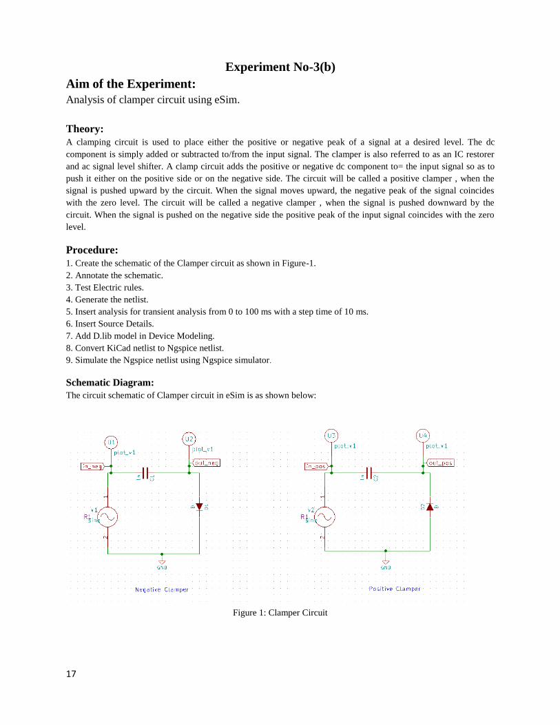
Experiment No-3(b)
Aim of the Experiment:
Analysis of clamper circuit using eSim.
Theory:
A clamping circuit is used to place either the positive or negative peak of a signal at a desired level. The dc
component is simply added or subtracted to/from the input signal. The clamper is also referred to as an IC restorer
and ac signal level shifter. A clamp circuit adds the positive or negative dc component to= the input signal so as to
push it either on the positive side or on the negative side. The circuit will be called a positive clamper , when the
signal is pushed upward by the circuit. When the signal moves upward, the negative peak of the signal coincides
with the zero level. The circuit will be called a negative clamper , when the signal is pushed downward by the
circuit. When the signal is pushed on the negative side the positive peak of the input signal coincides with the zero
level.
Procedure:
1. Create the schematic of the Clamper circuit as shown in Figure-1.
2. Annotate the schematic.
3. Test Electric rules.
4. Generate the netlist.
5. Insert analysis for transient analysis from 0 to 100 ms with a step time of 10 ms.
6. Insert Source Details.
7. Add D.lib model in Device Modeling.
8. Convert KiCad netlist to Ngspice netlist.
9. Simulate the Ngspice netlist using Ngspice simulator.
Schematic Diagram:
The circuit schematic of Clamper circuit in eSim is as shown below:
Figure 1: Clamper Circuit

18
Source Parameters:
Following are the input sine wave parameters:
1. Enter Offset Value- 0
2. Enter Amplitude - 5
3. Enter Frequency- 50
4. Enter Delay Time- 0
5. Enter Damping Factor- 0
Simulation Results:
Figure 2: Positive Clamper Python Plot Figure 3: Negative Clamper Python Plot
Figure 4: Positive Clamper Ngspice Plot Figure 5: Negative Clamper Ngspice Plot
Conclusion:
Thus, we have studied the diode application as a clamper circuit using eSim and we get the appropriate waveforms.
19
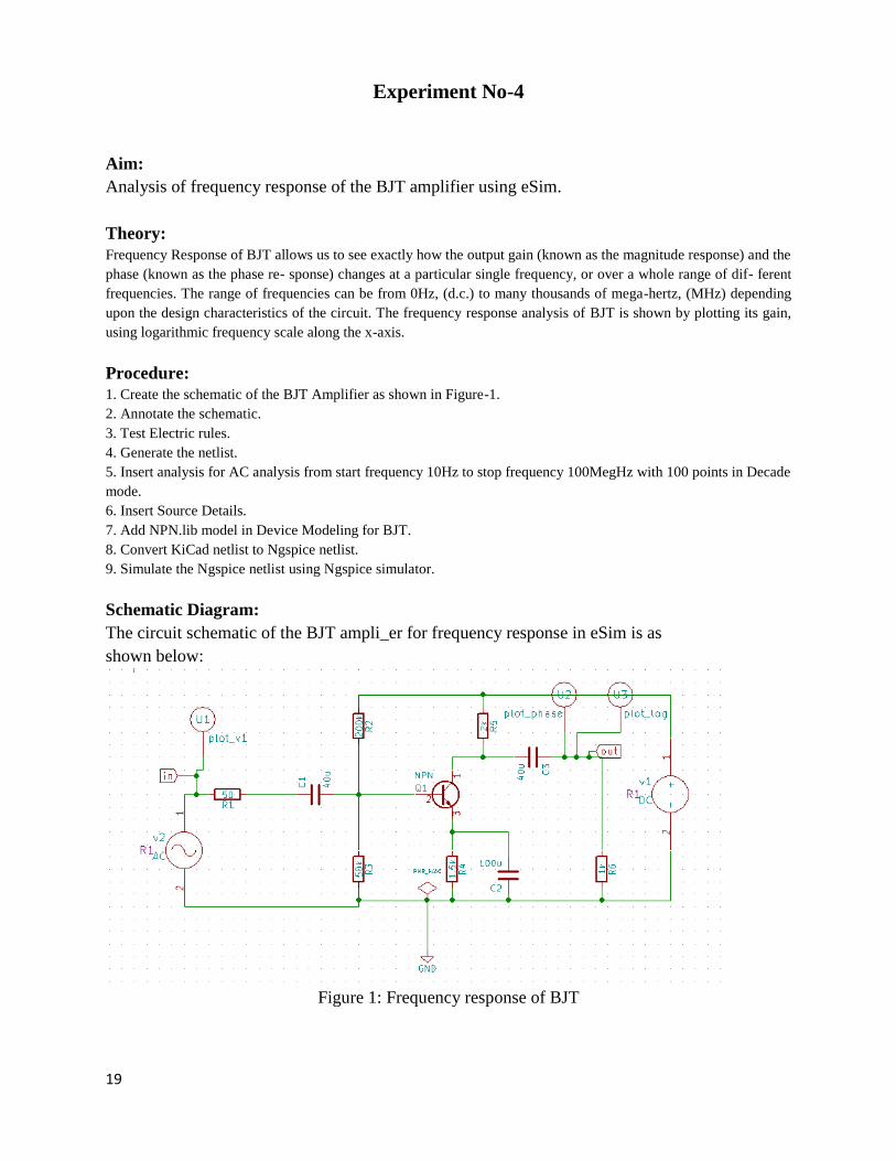
Experiment No-4
Aim:
Analysis of frequency response of the BJT amplifier using eSim.
Theory:
Frequency Response of BJT allows us to see exactly how the output gain (known as the magnitude response) and the
phase (known as the phase re- sponse) changes at a particular single frequency, or over a whole range of dif- ferent
frequencies. The range of frequencies can be from 0Hz, (d.c.) to many thousands of mega-hertz, (MHz) depending
upon the design characteristics of the circuit. The frequency response analysis of BJT is shown by plotting its gain,
using logarithmic frequency scale along the x-axis.
Procedure:
1. Create the schematic of the BJT Amplifier as shown in Figure-1.
2. Annotate the schematic.
3. Test Electric rules.
4. Generate the netlist.
5. Insert analysis for AC analysis from start frequency 10Hz to stop frequency 100MegHz with 100 points in Decade
mode.
6. Insert Source Details.
7. Add NPN.lib model in Device Modeling for BJT.
8. Convert KiCad netlist to Ngspice netlist.
9. Simulate the Ngspice netlist using Ngspice simulator.
Schematic Diagram:
The circuit schematic of the BJT ampli_er for frequency response in eSim is as
shown below:
Figure 1: Frequency response of BJT

20
Source Parameters:
For DC Voltage Source (V1):
1. Enter Value for V1 - 10
For AC Voltage Source (V2):
1. Enter Amplitude Value - 0.5
2. Enter Phase Value – 0
Simulation Results:
Figure 2: Ngspice Input Plot
Figure 3: Ngspice Output Frequency Plot Figure 4: Ngspice Output Phase Plot
Conclusion: Thus, we have studied the frequency response of the BJT amplifier using eSim and we get the appropriate
waveforms.
21
Cycle-II
(Signal & System)

22
Experiment No-1
AIM: -
To write a MATLAB program to perform some basic operation on matrices such as addition,
subtraction, multiplication.
SOFTWARE REQURIED:-
1.MATLAB R2010a.
2.Windows XP SP2.
THEORY:-
MATLAB, which stands for MATrix LABoratory, is a state-of-the-art mathematical software
package, which is used extensively in both academia and industry. It is an interactive program
for numerical computation and data visualization, which along with its programming capabilities
provides a very useful tool for almost all areas of science and engineering. Unlike other
mathematical packages, such as MAPLE or MATHEMATICA, MATLAB cannot perform
symbolic manipulations without the use of additional Toolboxes. It remains however, one of the
leading software packages for numerical computation. As you might guess from its name,
MATLAB deals mainly with matrices. A scalar is a 1-by-1 matrix and a row vector of length say
5, is a 1-by-5 matrix.. One of the many advantages of MATLAB is the natural notation used. It
looks a lot like the notation that you encounter in a linear algebra. This makes the use of the
program especially easy and it is what makes MATLAB a natural choice for numerical
computations. The purpose of this experiment is to familiarize MATLAB, by introducing the
basic features and commands of the program.
Built in Functions:
1. Scalar Functions:
Certain MATLAB functions are essentially used on scalars, but operate element-wise when
applied to a matrix (or vector). They are summarized below.
1. sin - trigonometric sine
2. cos - trigonometric cosine
3. tan - trigonometric tangent
4. asin - trigonometric inverse sine (arcsine)
5. acos - trigonometric inverse cosine (arccosine)
6. atan - trigonometric inverse tangent (arctangent)
7. exp - exponential
8. log - natural logarithm
9. abs - absolute value
10. sqrt - square root
11. rem - remainder
12. round - round towards nearest integer
13. floor - round towards negative infinity
14. ceil - round towards positive infinity
2. Vector Functions:
Other MATLAB functions operate essentially on vectors returning a scalar value. Some of
these functions are given below.
1. max largest component : get the row in which the maximum element lies
23
2. min smallest component
3. length length of a vector
4. sort sort in ascending order
5. sum sum of elements
6. prod product of elements
7. median median value
8. mean mean value std standard deviation
3. Matrix Functions:
Much of MATLAB‟ s power comes from its matrix functions. These can be further separated
into two sub-categories.
The first one consists of convenient matrix building functions, some of which are given
below.
1. eye - identity matrix
2. zeros - matrix of zeros
3. ones - matrix of ones
4. diag - extract diagonal of a matrix or create diagonal matrices
5. triu - upper triangular part of a matrix
6. tril - lower triangular part of a matrix
7. rand - randomly generated matrix
commands in the second sub-category of matrix functions are
1. size size of a matrix
2. det determinant of a square matrix
3. inv inverse of a matrix
4. rank rank of a matrix
5. rref reduced row echelon form
6. eig eigenvalues and eigenvectors
7. poly characteristic polynomial
PROCEDURE:-
Open MATLAB
Open new M-file
Type the program
Save in current directory
Compile and Run the program
For the output see command window\ Figure window
PROGRAM:-
clc;
close all;
clear all;
a=[1 2 -9 ; 2 -1 2; 3 -4 3];
b=[1 2 3; 4 5 6; 7 8 9];
disp('The matrix a= ');
a
disp('The matrix b= ');
b
% to find sum of a and b
c=a+b;
disp('The sum of a and b is ');

24
c
% to find difference of a and b
d=a-b;
disp('The difference of a and b is ');
d
%to find multiplication of a and b
e=a*b;
disp('The product of a and b is ');
e
OUTPUT:-
The matrix a=
a =
1 2 -9
2 -1 2
3 -4 3
The matrix b=
b =
1 2 3
4 5 6
7 8 9
The sum of a and b is
c =
2 4 -6
6 4 8
10 4 12
The difference of a and b is
d =
0 0 -12
-2 -6 -4
-4 -12 -6
The product of a and b is
e =
-54 -60 -66
12 15 18
8 10 12
RESULT:-
Finding addition, subtraction, multiplication using MATLAB was Successfully completed.

25
Experiment No-2
AIM:- To write a “MATLAB” Program to generate various signals and sequences,such as unit
impulse, unit step, unit ramp, sinusoidal,square,saw tooth,triangular,sinc signals.
SOFTWARE REQURIED:-
1.MATLAB R2010a.
2.Windows XP SP2.
THEORY:-
UNIT IMPULSE FUNCTION:
One of the more useful functions in the study of linear systems is the "unit impulse function."
An ideal impulse function is a function that is zero everywhere but at the origin, where it is
infinitely high. However, the area of the impulse is finite. This is, at first hard to visualize but
we can do so by using the graphs shown below.

26
UNIT STEP FUNCTION
The unit step function and the impulse function are considered to be fundamental functions in
engineering, and it is strongly recommended that the reader becomes very familiar with both of
these functions.
The unit step function, also known as the Heaviside function, is defined as such:
Sinc Function
There is a particular form that appears so frequently in communications engineering, that we
give it its own name. This function is called the "Sinc function and discussed below
The Sinc function is defined in the following manner:
And Sinc(0)=1
The value of sinc(x) is defined as 1 at x = 0, since
Rect Function
The Rect Function is a function which produces a rectangular centered at t = 0. The Rect
function pulse also has a height of 1. The Sinc function and the rectangular function form a
Fourier transform pair. A Rect function can be written in the form:
where the pulse is centered at X and has widthY. We can define the impulse function above in
terms of the rectangle function by centering the pulse at zero (X = 0), setting it's height to 1/A
and setting the pulse width to A, which approaches zero:
We can also construct a Rect function out of a pair of unit step functions
Here, both unit step functions are set a distance of Y/2 away from the center point of (t - X).
SAW TOOTH:-
The sawtooth wave (or saw wave) is a kind of non-sinusoidal waveform. It is named a sawtooth
based on its resemblance to the teeth on the blade of a saw. The convention is that a sawtooth
wave ramps upward and then sharply drops. However, there are also sawtooth waves in which
27
the wave ramps downward and then sharply rises. The latter type of sawtooth wave is called a
'reverse sawtooth wave' or 'inverse sawtooth wave'. As audio signals, the two orientations of
sawtooth wave sound identical. The piecewise linear function based on the floor function of time
t, is an example of a sawtooth wave with period 1.
TRIANGLE WAVE
A triangle wave is a non-sinusoidal waveform named for its triangular shape.A bandlimited
triangle wave pictured in the time domain (top) and frequency domain (bottom). The
fundamental is at 220 Hz (A2).Like a square wave, the triangle wave contains only odd
harmonics. However, the higher harmonics roll off much faster than in a square wave
(proportional to the inverse square of the harmonic number as opposed to just the inverse).It is
possible to approximate a triangle wave with additive synthesis by adding odd harmonics of the
fundamental, multiplying every (4n..1)th harmonic by �1 (or changing its phase by �), and
rolling off the harmonics by the inverse square of their relative frequency to the fundamental.
This infinite Fourier series converges to the triangle wave:
Sinusoidal Signal Generation
The sine wave or sinusoid is a mathematical function that describes a smooth repetitive
oscillation. It occurs often in pure mathematics, as well as physics, signal processing,
electrical engineering and many other fields. Its most basic form as a function of time (t)
is:
where:
• A, the amplitude, is the peak deviation of the function from its center position.
• the angular frequency, specifies how many oscillations occur in a unit time
interval, in radians per second
• the phase, specifies where in its cycle the oscillation begins at t = 0.
A sampled sinusoid may be written as:
where f is the signal frequency, fs is the sampling frequency, � is the phase and A is the
amplitude of the signal.
PROCEDURE:-
Open MATLAB
Open new M-file
Type the program
Save in current directory
Compile and Run the program
For the output see command window\ Figure window

28
PROGRAM:-
%unit impulse function%
clc;
clear all;
close all;
t=-10:1:10;
x=(t==0);
subplot(2,1,1);
plot(t,x,'g');
xlabel('time');
ylabel('amplitude');
title('unit impulse function');
subplot(2,1,2);
stem(t,x,'r');
xlabel('time');
ylabel('amplitude');
title('unit impulse discreat function');
%unit step function%
clc;
clear all;
close all;
N=100;
t=1:100;
x=ones(1,N);
subplot(2,1,1);
plot(t,x,'g');
xlabel('time');
ylabel('amplitude');
title('unit step function');
subplot(2,1,2);
stem(t,x,'r');
xlabel('time');
ylabel('amplitude');
title('unit step discreat function');
%unit ramp function%
clc;
clear all;
close all;
t=0:20;
x=t;
subplot(2,1,1);
plot(t,x,'g');
xlabel('time');
ylabel('amplitude');
title('unit ramp function');
subplot(2,1,2);
stem(t,x,'r');

29
xlabel('time');
ylabel('amplitude');
title('unit ramp discreat function');
%sinusoidal function%
clc;
clear all;
close all;
t=0:0.01:2;
x=sin(2*pi*t);
subplot(2,1,1);
plot(t,x,'g');
xlabel('time');
ylabel('amplitude');
title('sinusoidal signal');
subplot(2,1,2);
stem(t,x,'r');
xlabel('time');
ylabel('amplitude');
title('sinusoidal sequence');
%square function%
clc;
clear all;
close all;
t=0:0.01:2;
x=square(2*pi*t);
subplot(2,1,1);
plot(t,x,'g');
xlabel('time');
ylabel('amplitude');
title('square signal');
subplot(2,1,2);
stem(t,x,'r');
xlabel('time');
ylabel('amplitude');
title('square sequence');
%sawtooth function%
clc;
clear all;
close all;
t=0:0.01:2;
x=sawtooth(2*pi*5*t);
subplot(2,1,1);
plot(t,x,'g');
xlabel('time');
ylabel('amplitude');
title('sawtooth signal');
subplot(2,1,2);
stem(t,x,'r');

30
xlabel('time');
ylabel('amplitude');
title('sawtooth sequence');
%trianguler function%
clc;
clear all;
close all;
t=0:0.01:2;
x=sawtooth(2*pi*5*t,0.5);
subplot(2,1,1);
plot(t,x,'g');
xlabel('time');
ylabel('amplitude');
title('trianguler signal');
subplot(2,1,2);
stem(t,x,'r');
xlabel('time');
ylabel('amplitude');
title('trianguler sequence');
%sinc function%
clc;
clear all;
close all;
t=linspace(-5,5);
x=sinc(t);
subplot(2,1,1);
plot(t,x,'g');
xlabel('time');
ylabel('amplitude');
title('sinc signal');
subplot(2,1,2);
stem(t,x,'r');
xlabel('time');
ylabel('amplitude');
title('sinc sequence');

31

32
EXPERIMENT No-3
AIM:-
To performs operations on signals and sequences such as addition, multiplication, scaling,
shifting, folding, computation of energy and average power.
SOFTWARE REQURIED:-
1.MATLAB R2010a.
2.Windows XP SP2.
THEORY:-
Basic Operation on Signals:
Time shifting: y(t)=x(t-T)The effect that a time shift has on the appearance of a signal If T is a
positive number, the time shifted signal, x (t -T ) gets shifted to the right, otherwise it gets shifted
left.
Signal Shifting and Delay:
Shifting : y(n)={x(n-k)} ; m=n-k; y=x;
Time reversal: Y(t)=y(-t) Time reversal _ips the signal about t = 0 as seen in
Figure 1.
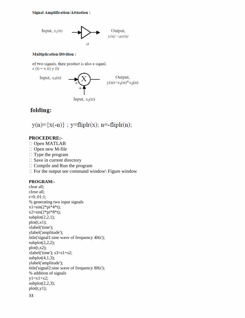
Signal Addition and Substraction :
Addition: any two signals can be added to form a third signal,
z (t) = x (t) + y (t)
33
PROCEDURE:-
Open MATLAB
Open new M-file
Type the program
Save in current directory
Compile and Run the program
For the output see command window\ Figure window
PROGRAM:-
clear all;
close all;
t=0:.01:1;
% generating two input signals
x1=sin(2*pi*4*t);
x2=sin(2*pi*8*t);
subplot(2,2,1);
plot(t,x1);
xlabel('time');
ylabel('amplitude');
title('signal1:sine wave of frequency 4Hz');
subplot(2,2,2);
plot(t,x2);
xlabel('time'); s3=s1+s2;
subplot(4,1,3);
ylabel('amplitude');
title('signal2:sine wave of frequency 8Hz');
% addition of signals
y1=x1+x2;
subplot(2,2,3);
plot(t,y1);

34
xlabel('time');
ylabel('amplitude');
title('resultant signal:signal1+signal2');
% multiplication of signals
y2=x1.*x2;
subplot(2,2,4);
plot(t,y2);
xlabel('time');
ylabel('amplitude');
title('resultant signal:dot product of signal1 and signal2');
% scaling of a signal1
A=10;
y3=A*x1;
figure;
subplot(2,2,1);
plot(t,x1);
xlabel('time');
ylabel('amplitude');
title('sine wave of frequency 4Hz')
subplot(2,2,2);
plot(t,y3);
xlabel('time');
ylabel('amplitude');
title('amplified input signal1 ');
% folding of a signal1
l1=length(x1);
nx=0:l1-1;
subplot(2,2,3);
plot(nx,x1);
xlabel('nx');
ylabel('amplitude');
title('sine wave of frequency 4Hz')
y4=fliplr(x1);
nf=-fliplr(nx);
subplot(2,2,4);
plot(nf,y4);
xlabel('nf');
ylabel('amplitude');
title('folded signal');
%shifting of a signal
figure;
t1=0:.01:pi;
x3=8*sin(2*pi*2*t1);
subplot(3,1,1);
plot(t1,x3);
xlabel('time t1');
ylabel('amplitude');
title('sine wave of frequency 2Hz');
subplot(3,1,2);
plot(t1+10,x3);
xlabel('t1+10');
ylabel('amplitude');
title('right shifted signal');
subplot(3,1,3);
plot(t1-10,x3);

35
xlabel('t1-10');
ylabel('amplitude');
title('left shifted signal');
%operations on sequences
n1=1:1:9;
s1=[1 2 3 0 5 8 0 2 4];
figure;
subplot(2,2,1);
stem(n1,s1);
xlabel('n1');
ylabel('amplitude');
title('input sequence1');
n2=-2:1:6;
s2=[1 1 2 4 6 0 5 3 6];
subplot(2,2,2);
stem(n2,s2);
xlabel('n2');
ylabel('amplitude');
title('input sequence2');
% addition of sequences
s3=s1+s2;
subplot(2,2,3);
stem(n1,s3);
xlabel('n1');
ylabel('amplitude');
title('sum of two sequences');
% multiplication of sequences
s4=s1.*s2;
subplot(2,2,4);
stem(n1,s4);
xlabel('n1');
ylabel('amplitude');
title('product of two sequences');
% scaling of a sequence
figure;
subplot(2,2,1);
stem(n1,s1);
xlabel('n1');
ylabel('amplitude');
title('input sequence1');
s5=4*s1;
subplot(2,2,2);
stem(n1,s5);
xlabel('n1');
ylabel('amplitude');
title('scaled sequence1');
subplot(2,2,3);
Department of ECE, MRCET BS Lab Manual
22
stem(n1-2,s1);
xlabel('n1');
ylabel('amplitude');
title('left shifted sequence1');

36
subplot(2,2,4);
stem(n1+2,s1);
xlabel('n1');
ylabel('amplitude');
title('right shifted sequence1');
% folding of a sequence
l2=length(s1);
nx1=0:l2-1;
figure;
subplot(2,1,1);
stem(nx1,s1);
xlabel('nx1');
ylabel('amplitude');
title('input sequence1');
s6=fliplr(s1);
nf2=-fliplr(nx1);
subplot(2,1,2);
stem(nf2,s6);
xlabel('nf2');
ylabel('amplitude');
title('folded sequence1');
% program for energy of a sequence
e1=sum(abs(z1).^2);
e1
% program for energy of a signal
t=0:pi:10*pi;
z2=cos(2*pi*50*t).^2;
e2=sum(abs(z2).^2);
e2
% program for power of a saequence
Department of ECE, MRCET BS Lab Manual
23
p1= (sum(abs(z1).^2))/length(z1);
p1
% program for power of a signal
p2=(sum(abs(z2).^2))/length(z2);
p2
OUTPUT:-
OUTPUT:
enter the input sequence [1 3 5 6]
e1 =
71
e2 =
4.0388
p1 =
17.7500
p2 =
0.3672
Result: Various operations on signals and sequences are performed.

37

38
EXPERIMENTY No-4
AIM: Finding even and odd part of the signal and sequence and also find real and imaginary
parts of signal.
Software Required:
Matlab software 7.0 and above.
Theory:
EVEN AND ODD PART OF A SIGNAL:
Any signal x(t) can be expressed as sum of even and odd components I e
X(t)=xe(t)+xo(t)
Program:
Clc;
close all;
clear all;
% Even and odd parts of a signal
t=0:.005:4*pi;
x=sin(t)+cos(t); % x(t)=sint(t)+cos(t)
subplot(2,2,1)
plot(t,x)
xlabel('t');
ylabel('amplitude')
title('input signal')
y=sin(-t)+cos(-t) % y=x(-t)
subplot(2,2,2)
plot(t,y)
xlabel('t');
ylabel('amplitude')
title('input signal with t=-t')
z=x+y
subplot(2,2,3)
plot(t,z/2)
xlabel('t');
ylabel('amplitude')
title('even part of the signal')
p=x-y

39
subplot(2,2,4)
plot(t,p/2)
xlabel('t');
ylabel('amplitude');
title('odd part of the signal');
% Even and odd parts of a sequence
z=[0,2+j*4,-3+j*2,5-j*1,-2-j*4,-j*3,0];
n=-3:3
% plotting real and imginary parts of the sequence
figure;
subplot( 2,1,1);
stem(n,real(z));
xlabel('n');
ylabel('amplitude');
title('real part of the complex sequence');
subplot( 2,1,2);
stem(n,imag(z));
xlabel('n');
ylabel('amplitude');
title('imaginary part of the complex sequence');
zc=conj(z);
zc_folded= fliplr(zc);
zc_even=.5*(z+zc_folded);
zc_odd=.5*(z-zc_folded);
% plotting even and odd parts of the sequence
figure;
subplot( 2,2,1);
Department of ECE, MRCET BS Lab Manual
32
stem(n,real(zc_even));
xlabel('n');
ylabel('amplitude');
title('real part of the even sequence');
subplot( 2,2,2);
stem(n,imag(zc_even));
xlabel('n');
ylabel('amplitude');
title('imaginary part of the even sequence');
subplot( 2,2,3);
stem(n,real(zc_odd));
xlabel('n');
ylabel('amplitude');
title('real part of the odd sequence');
subplot( 2,2,4);
stem(n,imag(zc_odd));
xlabel('n');
ylabel('amplitude');
title('imaginary part of the odd sequence');
RESULT: Even and odd part of the signal and sequence is computed.

40
OUTPUT:

41
EXPERIMENTY No-5
AIM: -
To find the output with linear convolution operation Using MATLAB Software.
SOFTWARE REQURIED:-
1.MATLAB R2010a.
2.Windows XP SP2. THEORY:-
Linear Convolution involves the following operations.
1. Folding
2. Multiplication
3. Addition
4. Shifting
These operations can be represented by a Mathematical Expression as follows:
Linear Convolution involves the following operations.
1. Folding
2. Multiplication
3. Addition
4. Shifting
These operations can be represented by a Mathematical Expression as follows:
PROCEDURE:-
Open MATLAB
Open new M-file
Type the program
Save in current directory
Compile and Run the program
For the output see command window\ Figure window
%program for convolution of two sequences
clc;
close all;
clear all;
%program for convolution of two sequences
x=input('enter input sequence');
h=input('enter impulse response');
y=conv(x,h);
subplot(3,1,1);
stem(x);
xlabel('n');
ylabel('x(n)');
title('input signal')
subplot(3,1,2);
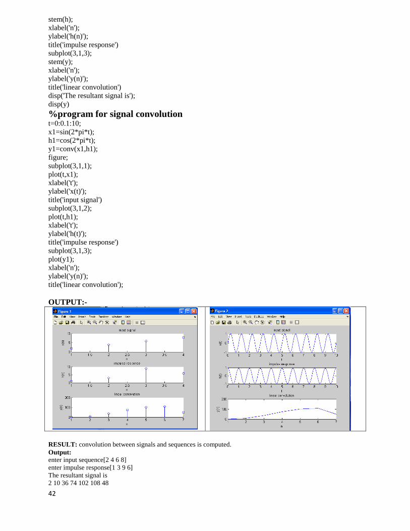
42
stem(h);
xlabel('n');
ylabel('h(n)');
title('impulse response')
subplot(3,1,3);
stem(y);
xlabel('n');
ylabel('y(n)');
title('linear convolution')
disp('The resultant signal is');
disp(y)
%program for signal convolution t=0:0.1:10;
x1=sin(2*pi*t);
h1=cos(2*pi*t);
y1=conv(x1,h1);
figure;
subplot(3,1,1);
plot(t,x1);
xlabel('t');
ylabel('x(t)');
title('input signal')
subplot(3,1,2);
plot(t,h1);
xlabel('t');
ylabel('h(t)');
title('impulse response')
subplot(3,1,3);
plot(y1);
xlabel('n');
ylabel('y(n)');
title('linear convolution');
OUTPUT:-
RESULT: convolution between signals and sequences is computed.
Output:
enter input sequence[2 4 6 8]
enter impulse response[1 3 9 6]
The resultant signal is
2 10 36 74 102 108 48

43
EXPERIMENT NO-6 AIM: -
To compute auto correlation and cross correlation between signals and Sequences.
Software Required:
Mat lab software 7.0 and above
Theory:
Correlations of sequences:
It is a measure of the degree to which two sequences are similar. Given two real-valued
sequences x(n) and y(n) of finite energy,
These operations can be represented by a Mathematical Expression asfollows:
Cross correlation
The index l is called the shift or lag parameter
Autocorrelation
Program: clc;
close all;
clear all;
% two input sequences
x=input('enter input sequence');
h=input('enter the impulse suquence');
subplot(2,2,1);
stem(x);
xlabel('n');
ylabel('x(n)');
title('input sequence');
subplot(2,2,2);
stem(h);
xlabel('n');
ylabel('h(n)');
title('impulse signal');
% cross correlation between two sequences
y=xcorr(x,h);
subplot(2,2,3);
stem(y);
xlabel('n');
ylabel('y(n)');
title(' cross correlation between two sequences ');
% auto correlation of input sequence
z=xcorr(x,x);

44
subplot(2,2,4);
stem(z);
xlabel('n');
ylabel('z(n)');
title('auto correlation of input sequence');
% cross correlation between two signals
% generating two input signals
t=0:0.2:10;
x1=3*exp(-2*t);
h1=exp(t);
figure;
subplot(2,2,1);
plot(t,x1);
xlabel('t');
ylabel('x1(t)');
title('input signal');
subplot(2,2,2);
plot(t,h1);
xlabel('t');
ylabel('h1(t)');
title('impulse signal');
% cross correlation
subplot(2,2,3);
z1=xcorr(x1,h1);
plot(z1);
xlabel('t');
ylabel('z1(t)');
title('cross correlation ');
% auto correlation
subplot(2,2,4);
z2=xcorr(x1,x1);
plot(z2);
xlabel('t');
ylabel('z2(t)');
title('auto correlation ');
Result: Auto correlation and Cross correlation between signals and sequences is computed.
Output: enter input sequence [1 2 5 7]
Enter the impulse sequence [2 6 0 5 3]
45
EXPERIMENT No-7(a)
AIM: Verify the Linearity of a given Discrete System.
Software Required:
Mat lab software 7.0 and above
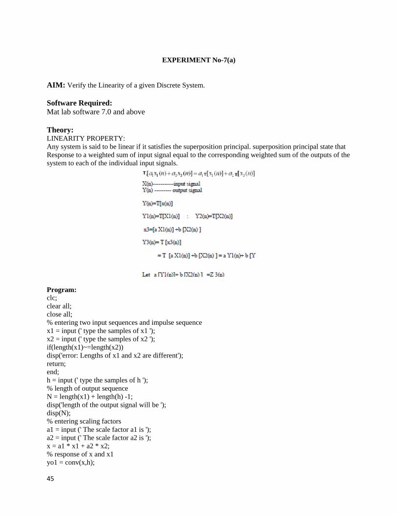
Theory: LINEARITY PROPERTY:
Any system is said to be linear if it satisfies the superposition principal. superposition principal state that
Response to a weighted sum of input signal equal to the corresponding weighted sum of the outputs of the
system to each of the individual input signals.
Program:
clc;
clear all;
close all;
% entering two input sequences and impulse sequence
x1 = input (' type the samples of x1 ');
x2 = input (' type the samples of x2 ');
if(length(x1)~=length(x2))
disp('error: Lengths of x1 and x2 are different');
return;
end;
h = input (' type the samples of h ');
% length of output sequence
N = length(x1) + length(h) -1;
disp('length of the output signal will be ');
disp(N);
% entering scaling factors
a1 = input (' The scale factor a1 is ');
a2 = input (' The scale factor a2 is ');
x = a1 * x1 + a2 * x2;
% response of x and x1
yo1 = conv(x,h);
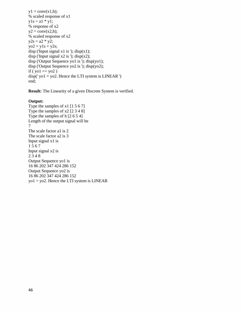
46
y1 = conv(x1,h);
% scaled response of x1
y1s = a1 * y1;
% response of x2
y2 = conv(x2,h);
% scaled response of x2
y2s = a2 * y2;
yo2 = y1s + y2s;
disp ('Input signal x1 is '); disp(x1);
disp ('Input signal x2 is '); disp(x2);
disp ('Output Sequence yo1 is '); disp(yo1);
disp ('Output Sequence yo2 is '); disp(yo2);
if ( yo1 == yo2 )
disp(' yo1 = yo2. Hence the LTI system is LINEAR ')
end;
Result: The Linearity of a given Discrete System is verified.
Output:
Type the samples of x1 [1 5 6 7]
Type the samples of x2 [2 3 4 8]
Type the samples of h [2 6 5 4]
Length of the output signal will be
7
The scale factor a1 is 2
The scale factor a2 is 3
Input signal x1 is
1 5 6 7
Input signal x2 is
2 3 4 8
Output Sequence yo1 is
16 86 202 347 424 286 152
Output Sequence yo2 is
16 86 202 347 424 286 152
yo1 = yo2. Hence the LTI system is LINEAR

47
EXPERIMENT No-7(b)
AIM: Verify the Time Invariance of a given Discrete System.
Software Required: Mat lab software 7.0 and above
Theory: TIME INVARIENT SYSTEMS(TI):
A system is called time invariant if its input – output characteristics do not change with time
X(t)---- input : Y(t) ---output
X(t-T) -----delay input by T seconds : Y(t-T) ------ Delayed output by T seconds
Program: clc;
clear all;
close all;
% entering two input sequences
x = input( ' Type the samples of signal x(n) ' );
h = input( ' Type the samples of signal h(n) ' );
% original response
y = conv(x,h);
disp( ' Enter a POSITIVE number for delay ' );
d = input( ' Desired delay of the signal is ' );
% delayed input
xd = [zeros(1,d), x];
nxd = 0 : length(xd)-1;
%delayed output
yd = conv(xd,h);
nyd = 0:length(yd)-1;
disp(' Original Input Signal x(n) is ');
disp(x);
disp(' Delayed Input Signal xd(n) is ');
disp(xd);
disp(' Original Output Signal y(n) is ');
disp(y);
disp(' Delayed Output Signal yd(n) is ');
disp(yd);
xp = [x , zeros(1,d)];
subplot(2,1,1);
stem(nxd,xp);
grid;
xlabel( ' Time Index n ' );
ylabel( ' x(n) ' );
title( ' Original Input Signal x(n) ' );
subplot(2,1,2);
stem(nxd,xd);
grid;
xlabel( ' Time Index n ' );

48
ylabel( ' xd(n) ' );
title( ' Delayed Input Signal xd(n) ' );
yp = [y zeros(1,d)];
figure;
subplot(2,1,1);
stem(nyd,yp);
grid;
xlabel( ' Time Index n ' );
ylabel( ' y(n) ' );
title( ' Original Output Signal y(n) ' );
subplot(2,1,2);
stem(nyd,yd);
grid;
xlabel( ' Time Index n ' );
ylabel( ' yd(n) ' );
title( ' Delayed Output Signal yd(n) ' );
Result: The Time Invariance of a given Discrete System is verified.
Output:
Type the samples of signal x(n) [2 3 4 6]
Type the samples of signal h(n) [1 2 3 8]
Enter a POSITIVE number for delay
Desired delay of the signal is 5
Original Input Signal x(n) is
2 3 4 6
Delayed Input Signal xd(n) is
0 0 0 0 0 2 3 4 6
Original Output Signal y(n) is
2 7 16 39 48 50 48
Delayed Output Signal yd(n) is
0 0 0 0 0 2 7 16 39 48 50 48

49
EXPERIMENT NO-8
AIM: Compute the Unit sample, unit step and sinusoidal response of the given LTI system and
verifying its stability
\
Software Required:
Mat lab software 7.0 and above
Theory:
A discrete time system performs an operation on an input signal based on predefined criteria to
produce a modified output signal. The input signal x(n) is the system excitation, and y(n) is the
system response. The transform\ operation is shown as,
If the input to the system is unit impulse i.e. x(n) = δ(n) then the output of the system is known
as impulse response denoted by h(n) where, h(n) = T[δ(n)] we know that any arbitrary sequence
x(n) can be represented as a weighted sum of discrete impulses. Now the system response is
given by,
For linear system (1) reduces to
given difference equation y(n)-y(n-1)+.9y(n-2)=x(n);
Program:

50
%given difference equation y(n)-y(n-1)+.9y(n-2)=x(n);
b=[1];
a=[1,-1,.9];
n =0:3:100;
%generating impulse signal
x1=(n==0);
%impulse response
h1=filter(b,a,x1);
subplot(3,1,1);
stem(n,h1);
xlabel('n');
ylabel('h(n)');
title('impulse response');
%generating step signal
x2=(n>0);
% step response
s=filter(b,a,x2);
subplot(3,1,2);
stem(n,s);
xlabel('n');
ylabel('s(n)')
title('step response');
%generating sinusoidal signal
t=0:0.1:2*pi;
x3=sin(t);
% sinusoidal response
h2=filter(b,a,x3);
subplot(3,1,3);
stem(h2);
xlabel('n');
ylabel('h(n)');
title('sin response');
% verifing stability
figure;
zplane(b,a);
Result: The Unit sample, unit step and sinusoidal response of the given LTI system is computed and its stability
verified. Hence all the poles lie inside the unit circle, so system is stable.
Output:

51
EXPERIMENT NO-9
AIM: -
To obtain Fourier Transform and Inverse Fourier Transform of a given signal / sequence and to
plot its Magnitude and Phase Spectra.
SOFTWARE REQURIED:-
1.MATLAB R2010a.
2.Windows XP SP2.
THEORY:-
Fourier Transform :
The Fourier transform as follows. Suppose that ƒ is a function which is zero outside of some interval
[−L/2, L/2]. Then for any T ≥ L we may expand ƒ in\ a Fourier series on the interval [−T/2,T/2], where the
"amount" of the wave e2πinx/T
in the Fourier series of ƒ is given by By definition Fourier Transform of
signal f(x) is defined as
Inverse Fourier Transform of signal F(w) is defined as
Program:
clc;
clear all;
close all;
fs=1000;
N=1024; % length of fft sequence
t=[0:N-1]*(1/fs);
% input signal
x=0.8*cos(2*pi*100*t);
subplot(3,1,1);
plot(t,x);
axis([0 0.05 -1 1]);
grid;
xlabel('t');
ylabel('amplitude');
title('input signal');
% magnitude spectrum
x1=fft(x);
k=0:N-1;
Xmag=abs(x1);
subplot(3,1,2);
plot(k,Xmag);
grid;
xlabel('t');
ylabel('amplitude');
title('magnitude of fft signal')
%phase spectrum

52
Xphase=angle(x1)*(180/pi);
subplot(3,1,3);
plot(k,Xphase);
grid;
xlabel('t');
ylabel('angle in degrees');
title('phase of fft signal');
Result: Magnitude and phase spectrum of FFT of a given signal is plotted.
Output:

53
EXPERIMENT-10
AIM: Write the program for locating poles and zeros and plotting pole-zero maps in s-plane and z-plane
for the given transfer function.
Software Required:
Matlab software 7.0 and above.
Theory:
Z-transforms
The Z-transform, like many other integral transforms, can be defined as either a one-sided or two-sided
transform. Bilateral Z-transform The bilateral or two-sided Z-transform of a discrete-time signal x[n] is
the function X(z) defined as
Unilateral Z-transform
Alternatively, in cases where x[n] is define
In signal processing, this definition is used when the signal is causal.
The roots of the equation P(z) = 0 correspond to the 'zeros' of X(z)
The roots of the equation Q(z) = 0 correspond to the 'poles' of X(z)
Example:
Program:
clc;
clear all;
close all;
%enter the numerator and denamenator cofficients in square brackets
num=input('enter the numerator cofficients');
den=input('enter the denamenator cofficients');

54
%find the transfer function using built-in function 'filt'
H=filt(num,den)
%find locations of zeros
z=zero(H);
disp('zeros are at ');
disp(z);
%find residues,pole locations and gain constant of H(z)
[r p k]=residuez(num,den);
disp('poles are at ');
disp(p);
%plot the pole zero map in z-plane
zplane(num,den);
title('pole-zero map of LTI system in z-plane');
% ploe-zero plot in s-plane
H1=tf(num,den) % find transfer function H(s)
[p1,z1]=pzmap(H1); % find the locations of poles and zeros
disp('poles ar at ');disp(p1);
disp('zeros ar at ');disp(z1);
figure;
%plot the pole-zero map in s-plane
pzmap(H1);
title('pole-zero map of LTI system in s-plane');
Result: Pole-zero maps are plotted in s-plane and z-plane for the given
transfer function.
Output:
enter the numerator cofficients[1 -1 4 3.5]
enter the denamenator cofficients[2 3 -2.5 6]
Transfer function:
1 - z^-1 + 4 z^-2 + 3.5 z^-3
------------------------------
2 + 3 z^-1 - 2.5 z^-2 + 6 z^-3
zeros are at
0.8402 + 2.1065i
0.8402 - 2.1065i
-0.6805
poles are at
-2.4874
0.4937 + 0.9810i
0.4937 - 0.9810i
Transfer function:
s^3 - s^2 + 4 s + 3.5
-------------------------
2 s^3 + 3 s^2 - 2.5 s + 6
poles ar at
-2.4874
0.4937 + 0.9810i
0.4937 - 0.9810i

55
zeros ar at
0.8402 + 2.1065i
0.8402 - 2.1065i
-0.6805

56
EXPERIMENT No-11
AIM: Verify the sampling theorem.
Software Required:
Matlab software 7.0 and above.
Theory:
Sampling Theorem:
A bandlimited signal can be reconstructed exactly if it is sampled at a rate atleast twice the maximum
frequency component in it." Figure 1 shows a signal g(t) that is bandlimited.
Figure 1: Spectrum of bandlimited signal g(t)
The maximum frequency component of g(t) is fm. To recover the signal g(t) exactly from its samples it
has to be sampled at a rate fs ≥ 2fm. The minimum required sampling rate fs = 2fm is called ' Nyquist rate
Proof: Let g(t) be a bandlimited signal whose bandwidth is fm (wm = 2πfm).
Figure 2: (a) Original signal g(t) (b) Spectrum G(w)
δ (t) is the sampling signal with fs = 1/T > 2fm.

57
Figure 3: (a) sampling signal δ (t) ) (b) Spectrum δ (w)
Figure 4: (a) sampled signal gs(t) (b) Spectrum Gs(w)
To recover the original signal G(w):
1. Filter with a Gate function, H2wm(w) of width 2wm Scale it by T.
Figure 5: Recovery of signal by filtering with a fiter of width 2wm
Aliasing ws < 2wm.

58
Figure 6: Aliasing due to inadequate sampling
Figure 7: Oversampled signal-avoids aliasing
Program:
Clc;
Clear all;
Close all;
t=-10:.01:10;
T=4;
fm=1/T;
x=cos(2*pi*fm*t);
subplot(2,2,1);
plot(t,x);
xlabel('time');
ylabel('x(t)');
title('continous time signal');
grid;
n1=-4:1:4;
fs1=1.6*fm;
fs2=2*fm;
fs3=8*fm;
x1=cos(2*pi*fm/fs1*n1);
subplot(2,2,2);
stem(n1,x1);
xlabel('time');
ylabel('x(n)');
title('discrete time signal with fs<2fm');
hold on;
subplot(2,2,2);
plot(n1,x1);
grid;
n2=-5:1:5;
x2=cos(2*pi*fm/fs2*n2);
subplot(2,2,3);
stem(n2,x2);
xlabel('time');
ylabel('x(n)');
title('discrete time signal with fs=2fm');
hold on;
subplot(2,2,3);
plot(n2,x2)
grid;

59
n3=-20:1:20;
x3=cos(2*pi*fm/fs3*n3);
subplot(2,2,4);
stem(n3,x3);
xlabel('time');
ylabel('x(n)');
title('discrete time signal with fs>2fm')
hold on;
subplot(2,2,4);
plot(n3,x3)
grid;
Result: Sampling theorem is verified.
OUTPUT:
60
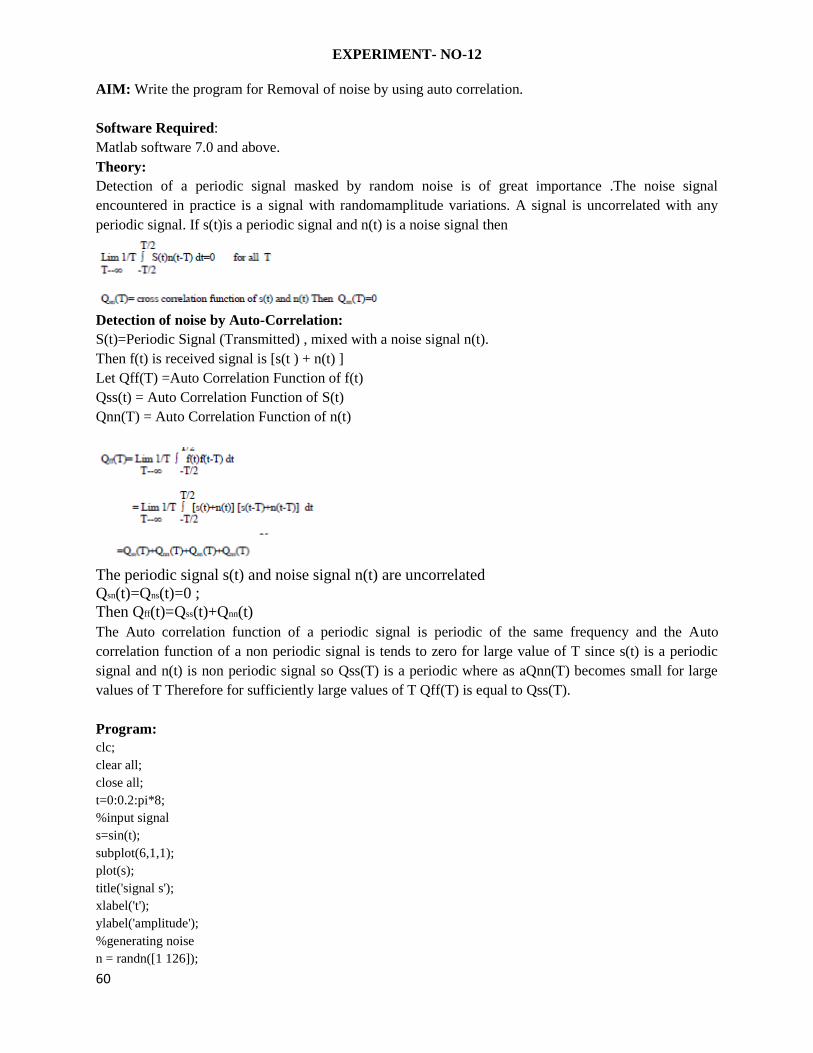
EXPERIMENT- NO-12
AIM: Write the program for Removal of noise by using auto correlation.
Software Required:
Matlab software 7.0 and above.
Theory:
Detection of a periodic signal masked by random noise is of great importance .The noise signal
encountered in practice is a signal with randomamplitude variations. A signal is uncorrelated with any
periodic signal. If s(t)is a periodic signal and n(t) is a noise signal then
Detection of noise by Auto-Correlation:
S(t)=Periodic Signal (Transmitted) , mixed with a noise signal n(t).
Then f(t) is received signal is [s(t ) + n(t) ]
Let Qff(T) =Auto Correlation Function of f(t)
Qss(t) = Auto Correlation Function of S(t)
Qnn(T) = Auto Correlation Function of n(t)
The periodic signal s(t) and noise signal n(t) are uncorrelated
Qsn(t)=Qns(t)=0 ;
Then Qff(t)=Qss(t)+Qnn(t)
The Auto correlation function of a periodic signal is periodic of the same frequency and the Auto
correlation function of a non periodic signal is tends to zero for large value of T since s(t) is a periodic
signal and n(t) is non periodic signal so Qss(T) is a periodic where as aQnn(T) becomes small for large
values of T Therefore for sufficiently large values of T Qff(T) is equal to Qss(T).
Program:
clc;
clear all;
close all;
t=0:0.2:pi*8;
%input signal
s=sin(t);
subplot(6,1,1);
plot(s);
title('signal s');
xlabel('t');
ylabel('amplitude');
%generating noise
n = randn([1 126]);

61
%noisy signal
f=s+n;
subplot(6,1,2)
plot(f);
title('signal f=s+n');
xlabel('t');
ylabel('amplitude');
%aucorrelation of input signal
as=xcorr(s,s);
subplot(6,1,3);
plot(as);
title('auto correlation of s');
xlabel('t');
ylabel('amplitude');
%aucorrelation of noise signal
an=xcorr(n,n);
subplot(6,1,4)
plot(an);
title('auto correlation of n');
xlabel('t');
ylabel('amplitude');
%aucorrelation of transmitted signal
cff=xcorr(f,f);
subplot(6,1,5)
plot(cff);
title('auto correlation of f');
xlabel('t');
ylabel('amplitude');
%aucorrelation of received signal
hh=as+an;
subplot(6,1,6)
plot(hh);
title('addition of as+an');
xlabel('t');
ylabel('amplitude');
Result:Removal of noise using autocorrelation is performed.
Output:
Related Documents