Lab. No. 4 1 2N3904 2N3904 10 kΩ 12 kΩ 470 Ω R X =15kΩ X +15 V -15 V 470 Ω 10 kΩ V IN - V OUT V IN + 12 kΩ Name: _________________________________________________ M A S S A C H U S E T T S I N S T I T U T E O F T E C H N O L O G Y DEPARTMENT OF ELECTRICAL ENGINEERING AND COMPUTER SCIENCE 6.101 Introductory Analog Electronics Laboratory Spring 2020 Laboratory No. 4 [Report Template on the web] READING ASSIGNMENT Neamen 3 rd Edition: pp. 593-596, pp. 578 [8.3.2] – 586 top Op-Amps For Everyone Chapter 3 (course website: “reference”) In this laboratory, you will investigate the performance of operational amplifiers in simple circuit configurations. We will discuss various aspects of operational amplifier behavior in class. In addition, you should have read at least the Chapter 3 in Op-Amps for Everyone, a reference from Texas Instruments. You can find this document in the class website under “Reference” as well as Prof Jim Roberge’s textbook Operational Amplifiers – Theory and Practice. Objective: Anyone can design circuits that operate in the midrange of specs. Real engineers understand the limitations, design near the limits and push the envelope – the reason for this lab. You will be using the LM741, which is one of the earliest of popular operational amplifiers, the LF356 which is a precision JFET-input op-amp with very low input bias current, wider open-loop bandwidth, higher slew rate, etc., the LM6132, a dual rail-to-rail op-amp, and the LM311 comparator. The lab starts with the differential pair, a key element of an op-amp and ends with a Fitbit-like heart rate lab. Acknowledgement: Special thanks to Texas Instruments for their generous donation of the LM311 comparators and the LM6132 op-amps. Experiment 1: Differential Transistor Pair [Long-Tailed Pair] The differential pair, either with either BJT or MOSFET, is the first stage of most integrated circuit operational amplifiers. In this experiment, you will investigate the performance of a differential amplifier input stage and examine its significant characteristics. Figure 1: Differential amplifier for experiment 1

Welcome message from author
This document is posted to help you gain knowledge. Please leave a comment to let me know what you think about it! Share it to your friends and learn new things together.
Transcript

Lab. No. 4 1
2N3904 2N3904
10 kΩ
12 kΩ
470 Ω
RX=15kΩ
X
+15 V
-15 V
470 Ω10 kΩ VIN -
VOUT
VIN +
12 kΩ
Name: _________________________________________________
M A S S A C H U S E T T S I N S T I T U T E O F T E C H N O L O G Y
DEPARTMENT OF ELECTRICAL ENGINEERING AND COMPUTER SCIENCE
6.101 Introductory Analog Electronics Laboratory Spring 2020
Laboratory No. 4 [Report Template on the web] READING ASSIGNMENT Neamen 3rd Edition: pp. 593-596, pp. 578 [8.3.2] – 586 top Op-Amps For Everyone Chapter 3 (course website: “reference”) In this laboratory, you will investigate the performance of operational amplifiers in simple circuit configurations. We will discuss various aspects of operational amplifier behavior in class. In addition, you should have read at least the Chapter 3 in Op-Amps for Everyone, a reference from Texas Instruments. You can find this document in the class website under “Reference” as well as Prof Jim Roberge’s textbook Operational Amplifiers – Theory and Practice. Objective: Anyone can design circuits that operate in the midrange of specs. Real engineers understand the limitations, design near the limits and push the envelope – the reason for this lab. You will be using the LM741, which is one of the earliest of popular operational amplifiers, the LF356 which is a precision JFET-input op-amp with very low input bias current, wider open-loop bandwidth, higher slew rate, etc., the LM6132, a dual rail-to-rail op-amp, and the LM311 comparator. The lab starts with the differential pair, a key element of an op-amp and ends with a Fitbit-like heart rate lab. Acknowledgement: Special thanks to Texas Instruments for their generous donation of the LM311 comparators and the LM6132 op-amps. Experiment 1: Differential Transistor Pair [Long-Tailed Pair] The differential pair, either with either BJT or MOSFET, is the first stage of most integrated circuit operational amplifiers. In this experiment, you will investigate the performance of a differential amplifier input stage and examine its significant characteristics.
Figure 1: Differential amplifier for experiment 1

Lab. No. 4 2
Consider the two 470 Ω “linearizing” resistors. For a common emitter amplifier with RL but no emitter resistor (not shown), the gain is -gmRL Adding in the emitter resistor the small signal gain is -RL/RE. Remember that the collector current is proportional to Vπ = Vbe.
One way to view this is that when an emitter resistor is added, Ve is no longer fixed at ground but increases with increasing current thus you have a local feedback loop that stabilizes the current. The same reasoning can be applied to the differential pair. Since Rx is large, the circuit from x to -15V can be considered a current source. Thus if the transistor on the right sources more current, the left transistor must source less.
[Please note that without the emitter linearizing resistors, this amplifier is operating without any feedback. Keep your eye on the purity of the output signal on your scope and see if there are any differences between the circuits with the emitter resistors and the ones without them. You may have to use a fairly large output swing in order to see any distortion.
1. Construct the differential amplifier of Figure 1.
a. COMMON MODE GAIN i. Connect a 1 kHz signal to both inputs vin+ and vin-. Since the inputs are
identical (common mode input), for ideal transistors, the output would be zero. Measure the common-mode gain:
Now measure the “single-ended” differential gain. You can do this by grounding the negative input and applying a signal to the positive input and by appropriately adjusting the result. *
[* This adjustment is required because we are not applying a true differential input voltage, but rather simulating one with a single input voltage. This has the effect of also applying an
average common-mode input voltage equal to at the same
time, so some of the output is due to common-mode gain, not just differential gain.] Q 1.1 Without the schematic, explain how can you tell which input is the positive input? Finally, measure the output-offset voltage [with no AC input signal] across the differential output terminals [collector-collector rather than second collector to ground]. Make sure the 12kΩ resistors are exactly equal to avoid generating an offset voltage due to unequal resistor values. 2. Now replace the emitter resistors with short circuits and repeat the measurements in step1 above.
)(** ebmbemc VVgVgI −==
Acm voutvin vin= ÷
+ + −
2
A vv
Adiff
out
in
cm= −+ 2.
22
0
2
+=
++=
−++invinvinvinv
Lab. No. 4 3
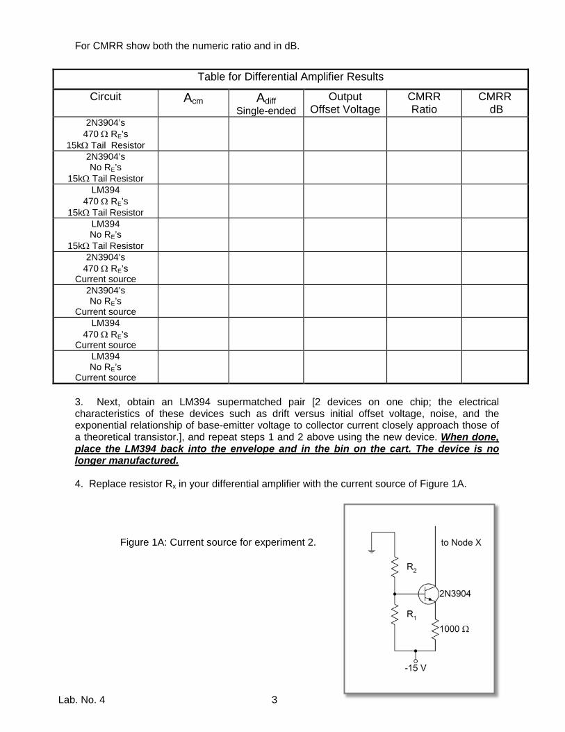
For CMRR show both the numeric ratio and in dB.
Table for Differential Amplifier Results
Circuit Acm Adiff Single-ended
Output Offset Voltage
CMRR Ratio
CMRR dB
2N3904’s 470 Ω RE’s
15kΩ Tail Resistor
2N3904’s No RE’s
15kΩ Tail Resistor
LM394 470 Ω RE’s
15kΩ Tail Resistor
LM394 No RE’s
15kΩ Tail Resistor
2N3904’s 470 Ω RE’s
Current source
2N3904’s No RE’s
Current source
LM394 470 Ω RE’s
Current source
LM394 No RE’s
Current source
3. Next, obtain an LM394 supermatched pair [2 devices on one chip; the electrical characteristics of these devices such as drift versus initial offset voltage, noise, and the exponential relationship of base-emitter voltage to collector current closely approach those of a theoretical transistor.], and repeat steps 1 and 2 above using the new device. When done, place the LM394 back into the envelope and in the bin on the cart. The device is no longer manufactured. 4. Replace resistor Rx in your differential amplifier with the current source of Figure 1A. Figure 1A: Current source for experiment 2.

Lab. No. 4 4
Repeat all your measurements in steps 1-3 above using the current source. Since R1 and R2 is used for biasing only, i.e. there are no AC input impedance considerations, we can choose R1 and R2 to be very low to make sure that transistor Beta does not affect the value of the current source. IMPORTANT: Design your current source to give exactly the same total current as that which flowed through the resistor RX in the previous circuit. [Use very stiff or bias stable voltage divider biasing, i.e. make the current through R1 and R2 very large compared to the transistor base current.]
5. Calculate the common-mode rejection ratios (CMRR) for all circuit configurations. Express your results in dB. Tabulate all your data from steps 1-5 in the table provided so that the various circuits can be easily compared. Q 1.2 Explain in your write up which configurations and devices are the best with respect to CMRR, voltage gain, and low offset voltage.
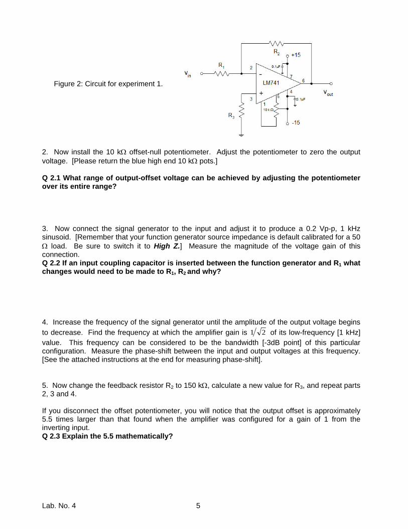
Checkoff 1: Show results of the measurements and explain which configuration has the best CMRR and lowest input offset voltage. [1.0 point] Experiment 2: The Inverting Configuration. In this experiment, you will be connecting a LM741 in the inverting configuration of Figure 2. You will learn to adjust the offset of the amplifier, measure its bandwidth and see how its performance is limited by its slew rate. 1. Construct the circuit of Figure 2. [Refer to the LM741 data sheet to make sure that you connect to the proper pins of your LM741]. Choose resistor values R1 = R2 = 15 kΩ and R3 = 7.5 kΩ and do not install the 10 kΩ potentiometer at this point. Ground the input vin and measure the output voltage [it will probably differ by some number of millivolts from zero]. This voltage is caused by the input offset voltage that can be modeled as a dc voltage source in series with the non-inverting input to the amplifier and the gain of the amplifier [in this case the gain is two for a voltage applied to the non-inverting input]. Calculate the corresponding input offset voltage and compare this value with that found on the LM741 data sheet.
cmrrAA
diff
cm
=
21 EEX III +=
v v v v
or v v v vIN be be IN
be be IN IN
+ −
+ −
− − − =
− = −1 2
1 2
0
( ) ( )( )Acm vout
vin vin gmRL
gm Rx REo
oRLr Rx RE o
RLRx RE
= ÷+ + −
=−
+ + +
=−
+ + +≈
−
+21 2 1 1 2 1 2
β
β
π β
Av
vR
Ror
g R Rr
if Rdiffout
indiff
L
E
m L LE= =
−
=
−=
−=
12 2 2
00; .β
π
Lab. No. 4 5
Figure 2: Circuit for experiment 1. 2. Now install the 10 kΩ offset-null potentiometer. Adjust the potentiometer to zero the output voltage. [Please return the blue high end 10 kΩ pots.] Q 2.1 What range of output-offset voltage can be achieved by adjusting the potentiometer over its entire range? 3. Now connect the signal generator to the input and adjust it to produce a 0.2 Vp-p, 1 kHz sinusoid. [Remember that your function generator source impedance is default calibrated for a 50 Ω load. Be sure to switch it to High Z.] Measure the magnitude of the voltage gain of this connection. Q 2.2 If an input coupling capacitor is inserted between the function generator and R1 what changes would need to be made to R1, R2 and why? 4. Increase the frequency of the signal generator until the amplitude of the output voltage begins to decrease. Find the frequency at which the amplifier gain is of its low-frequency [1 kHz] value. This frequency can be considered to be the bandwidth [-3dB point] of this particular configuration. Measure the phase-shift between the input and output voltages at this frequency. [See the attached instructions at the end for measuring phase-shift]. 5. Now change the feedback resistor R2 to 150 kΩ, calculate a new value for R3, and repeat parts 2, 3 and 4. If you disconnect the offset potentiometer, you will notice that the output offset is approximately 5.5 times larger than that found when the amplifier was configured for a gain of 1 from the inverting input. Q 2.3 Explain the 5.5 mathematically?
1 2
Lab. No. 4 6
Q 2.4 Why did we change R3.? Q 2.5 What is the ideal value of R3 relative to the values of R1 and R2?
Notice that while the inverting amplifier gain is a factor of 10 larger than that of the first configuration, the bandwidth is approximately a factor of 5.5 lower. If you were to examine this configuration for other values of gain, you would find out that the higher the gain, the lower the bandwidth; specifically, that the product of (one plus the gain) times the bandwidth is a constant.
6. With the signal generator set to the bandwidth frequency [-3dB point] for the gain of -10, which you found in part 5, increase the amplitude of the input voltage until the output voltage begins to distort [i.e. it will no longer look sinusoidal, but more like a triangle wave]. At this point, the amplifier has reached its slew-rate limit. The slew-rate limit of an operational amplifier is caused by a current source within the amplifier [biasing the first stage, the input differential stage, of the amplifier] that limits the amount of current that can be supplied by the first stage of the amplifier. When the amplifier is pushed to the point that this limit is reached, it can no longer function properly. The slew-rate limit manifests itself as a maximum value of dvout/dt for the amplifier because there is an internal amplifier capacitance that must be charged by the first-stage output current and a first-stage current limit thus corresponds to a maximum dv/dt for this capacitor. With the input amplitude set to the value at which the output voltage just starts to distort, calculate the maximum value of dvout/dt on the output voltage. Q 2.6 How does this value compare with the slew-rate value that is found in the LM741 spec sheet? 7. Reduce the frequency of the input voltage by a factor of 5 and again measure the slew rate of the amplifier by finding the value of dvout/dt for which the output voltage begins to distort. Compare this to the earlier measurement of slew rate. 8. With the signal generator set to a frequency of 1 kHz, increase the amplitude of the input voltage until the output voltage saturates [the top of the sine wave just begins to flatten]. Measure the saturation voltage of the amplifier [both positive and negative] and compare these values with the magnitudes of the positive and negative supply voltage. Repeat this measurement using a load resistor of 510 ohms connected between output and ground. Q 2.7 How do the saturation voltages with the load resistor differ from the test using the amplifier without a load resistance [infinite load impedance]?
Lab. No. 4 7
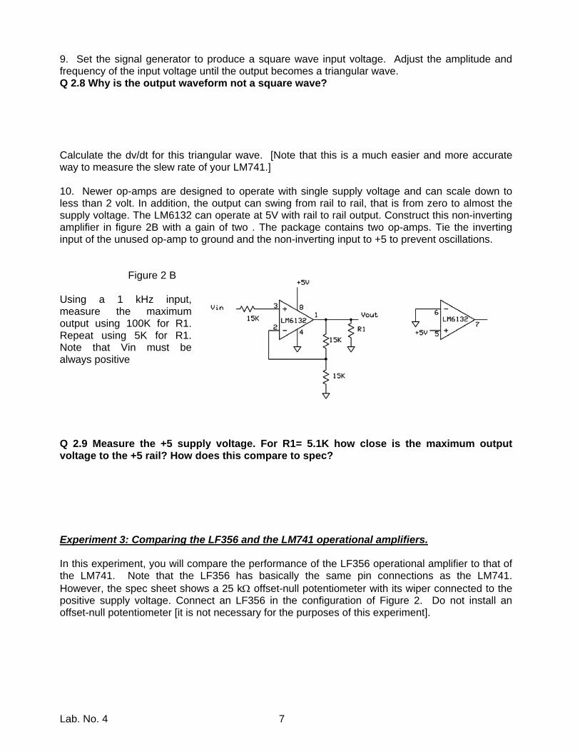
9. Set the signal generator to produce a square wave input voltage. Adjust the amplitude and frequency of the input voltage until the output becomes a triangular wave. Q 2.8 Why is the output waveform not a square wave? Calculate the dv/dt for this triangular wave. [Note that this is a much easier and more accurate way to measure the slew rate of your LM741.] 10. Newer op-amps are designed to operate with single supply voltage and can scale down to less than 2 volt. In addition, the output can swing from rail to rail, that is from zero to almost the supply voltage. The LM6132 can operate at 5V with rail to rail output. Construct this non-inverting amplifier in figure 2B with a gain of two . The package contains two op-amps. Tie the inverting input of the unused op-amp to ground and the non-inverting input to +5 to prevent oscillations. Figure 2 B Using a 1 kHz input, measure the maximum output using 100K for R1. Repeat using 5K for R1. Note that Vin must be always positive Q 2.9 Measure the +5 supply voltage. For R1= 5.1K how close is the maximum output voltage to the +5 rail? How does this compare to spec? Experiment 3: Comparing the LF356 and the LM741 operational amplifiers. In this experiment, you will compare the performance of the LF356 operational amplifier to that of the LM741. Note that the LF356 has basically the same pin connections as the LM741. However, the spec sheet shows a 25 kΩ offset-null potentiometer with its wiper connected to the positive supply voltage. Connect an LF356 in the configuration of Figure 2. Do not install an offset-null potentiometer [it is not necessary for the purposes of this experiment].

Lab. No. 4 8
1. Q 3.1 Measure the bandwidth of the amplifier built with an LF356 using a feedback R2 to 150 kΩ. How does this compare with your measurement with the value given in the spec sheet? 2. Measure the slew rate of the LF356. You may find it difficult to make an accurate measurement; make an educated guess. Q 3.2 How does the measured slew rate of the LF 356 compare with the value found in the spec sheet? How does the slew rate compare with the LM 741 slew rate? Experiment 3: Common amplifier configurations. In the previous experiments, you examined the inverting op-amp configuration. In this experiment, you will examine other common configurations. These circuits are shown in Figure 2. Use a LM741 op amp for these experiments, except use the LM311 comparator for figure 3c, the comparator circuit. 1. Figure 3[a] shows the configuration of an inverting adder. Select the resistor values such that vout = -(1.5vin1 + 3 vin2). Select the value of resistor R4 to minimize the effects of input bias current. Build the circuit and confirm its performance by applying DC voltages to each input. One voltage can be the +5 V DC supply, the other can come from your function generator offset voltage [turn off the AC output]. Be sure not to drive your output into saturation with large input voltages. Figure 3 Circuits for experiment 3.

Lab. No. 4 9
2. Construct the voltage follower [unity-gain buffer] of Figure 3[b]. Omit the resistor to ground. Q 3.3 If you do not use a coupling capacitor, the circuit should work properly. Why?
Find the frequency at which the gain drops to [-3dB] of the low-frequency value. Insert a 10 MΩ resistor in series with the input of the voltage follower [to simulate a voltage source with a high source impedance]. Recognizing that a key feature of the voltage follower is its high input impedance, one would expect that there would be no change in the gain of the follower circuit. Q 3.4 Your scope probe has a resistance from tip to ground of 10 MΩ. What effect will your scope probe have if you use it to measure the input voltage (pin 3) to this op-amp? You will observe that in fact the gain does not change at low frequencies. However, you will notice that the gain drops off fairly rapidly with frequency. This is due to the presence of parasitic capacitance in the circuit. In this case, the high impedance of the source resistance in combination with a small amount of capacitance between the input to the op-amp and ground forms an RC filter that reduces the gain of the op-amp. Measure the frequency at which the amplifier gain drops to [-3dB] of the low-frequency value in this configuration and use this measurement to estimate the value of the parasitic capacitance. Note that the effects of stray capacitances [along with issues such as input bias current] limit the magnitude of resistance values that can be used in practical operational amplifier circuit configurations. 3. Figure 3[c] shows the circuit configuration for a comparator. (Note: the device is a LM311 with different pinouts.) Resistors R1 and R2 set the voltage level at which the circuit output will switch between positive and negative saturation. Due to the internal capacitor required to stabilize IC’s designed for negative-feedback amplifier operation, and the nature of the output stage, driving such an amplifier into saturation can require a long time for it to recover once the input stimulus changes. This makes the op-amp a pretty bad choice for use as a comparator at higher frequencies. [Comparators are usually operated without feedback.] Thus, a series of products specifically designed for use as comparators has been developed. These devices have open collector outputs and thus require an external resistor connected to the positive supply rail in order to operate properly. The size of the external resistor will depend on the amount of current needed to drive the load when the output transistor is “on” [saturated] and current flows from the positive supply through the load resistor to the load on the output. Typical resistor values are in the 1.0kΩ to 10kΩ range. This resistor is labeled RPU (R pull up) in the schematic. Also please note that even though the comparator is connected to both the +15 v and –15v supplies, the output swings only from ground to +15 volts in the circuit shown. [The output can be arranged to drive loads referred to the positive supply or the negative supply, as well as a load referred to ground as illustrated here. See the LM311 spec sheet for more info on the use of this device. If your comparator oscillates at the transition (from low to high or high to low) point, see the spec sheet application hints for ways to cure this.] • Construct a comparator that switches when the input voltage reaches a level of approximately
+5.0 V. Use standard 5% resistor values, 1 each for R1 and R2.
1 2
1 2

Lab. No. 4 10
• Measure the time that it takes the comparator to switch between the positive and negative
[high and low] saturation voltages.
4. Figure 3[d] shows the circuit configuration for a Schmitt trigger. A Schmitt trigger uses the operational amplifier [good for low frequencies only!] as a comparator along with positive feedback to create a “hysteretic” switch. If you analyze this circuit, you will find that if the output of the Schmitt trigger is positive, the input will have to be raised to some fraction of the output voltage before the output will switch to a negative value. It will then require the same level of negative input voltage before the output will switch positive. This circuit can be used to “compare” noisy signals that are expected to have enough difference in their values to exceed the design thresholds. In other words, the Schmitt trigger will not switch output states when only noise is presented to the input, if the noise is lower than the thresholds. The standard comparator in figure 2[c] above will change state easily [and often!] with a noisy input. Find R1 and R2 such that the threshold-voltage of the Schmitt trigger is approximately 1/3 the magnitude of the supply voltage. Construct the circuit and verify your calculation. 5. In Figure 3[e] a capacitor and resistor have been added to the Schmitt trigger of Figure 2[d] to produce an oscillator. Show the output waveform in your lab report; also show the capacitor charging and discharging voltage waveform. Q 3.5 How does the value of the hysteresis threshold voltage affect the frequency of oscillation? Q 3.6 Find values of R3 and C to produce an oscillation at approximately 1000 Hz. Measure the actual frequency using your scope. Then, increase the frequency to 100 kHz. 1000 Hz R3__________ C ______________ 100 KHz R3__________ C ______________ Q 3.7 Sketch and show the wave shape at 100KHz and 1Khz. How does the wave shape at 100 kHz compare with the wave shape at 1 kHz? Why do you think this occurs?

Lab. No. 4 11
Now, reconfigure this circuit and replace the LM741 with an LM311 comparator chip. (The pinouts will have to be changed.) Once again compare the waveforms at 1kHz and 100kHz. [For this exercise, use a 4.7k pull-up resistor for LM311 and now tie the emitter (pin 1) of the LM311 to -15V.] Q 3.8 How does the wave shape at 100 kHz compare with the wave shape at 1 kHz? What have we done to improve the waveform shape at 100 kHz? Experiment 4: Integrators, filters, etc.
In this experiment you will use capacitors as well as resistors in the feedback circuits of your operational amplifier. All of these circuits can be thought of either in time domain terms [differential equations] or frequency domain terms [transfer functions], depending upon the application.
Figure 4: Circuits for experiment 4.
1. Figure 4[a] shows the configuration of a low-pass filter/integrator (LPF). In the frequency domain, this circuit corresponds to a low-pass filter. For this experiment, design this circuit to be an integrator at a frequency of 10,000 Hz. Because this will not be a perfect integrator, you will want to make sure that the phase-shift between the output and the input will at least be -85o [an ideal integrator would have a phase-shift of -90o]. Design the circuit to have a low-frequency gain of −10. Show your calculations. Measure the magnitude and phase angle of the circuit transfer function at 10,000 Hz to verify your calculations. [NOTE: In order for the integrator to be integrating at 10,000 Hz, you must be well down on the slope of the response plot caused by the pole determined by R2 and the 100 nF capacitor in the feedback loop. It is best to keep a one-decade difference between the corner frequency and the frequency where you want the integrator to work. Remember, that while we draw straight lines to show gain at the corner frequencies or break points, the actual response change is gradual, and this break point is only -3dB, which corresponds to a phase shift of only -45 degrees. So please
vout
[a] Integrator/Low Pass Filter [b] Differentiator/High Pass Filter
-
+
LF356
2
34
7
6
12 kΩ
vin
10 nF1 kΩ
12 kΩ
vout-
+
+15
-15
LF356
2
34
7
6
R1
R3
R2
vin
100 nF
0.1µF
0.1µF
0.1µF
+15
-15
0.1µF

Lab. No. 4 12
choose your -3dB point with this in mind.] Checkoff 2: Explain how phase shift varies with frequency and show measurement on the scope. [1.2 point] Rough plot the measured magnitude of the LPF transfer function as a function of frequency. On the same plot, draw the asymptotes for this transfer function that you would expect based upon the calculated transfer function.
Q 4.1 What is the bandwidth of this filter? Apply a square wave to this circuit. Observe the output as you vary the input frequency from 10 kHz down towards the –3dB frequency. Verify that this circuit does indeed operate as an integrator. Q 4.2 For what frequencies does this circuit produce an output waveform that is the integral of the input? At what frequency does the output start to depart from the ideal waveform?
2. Figure 4[b] shows the circuit configuration for a differentiator. In the frequency domain, this circuit corresponds to a high-pass filter.
Q 4.3 For what frequencies should this differentiator produce an output waveform that is the derivative of the input?

Lab. No. 4 13
Apply a triangular wave to this circuit. Observe the output as a function of frequency. Verify that this circuit does indeed operate as a differentiator. Q 4.4 At what frequency does the performance of your differentiator begin to deteriorate? In the frequency domain, this circuit can be thought of a high-pass filter. Rough plot its measured sine-wave frequency response from 1 Hz to 100 kHz. On the same plot, draw the asymptotes for this transfer function that you would expect based upon the calculated transfer function.
Experiment 5: A few other op-amp applications. 1. Construct the circuit of Figure 5[a]. With the function generator set to produce a 5 V p-p sinusoid at 60 Hz, observe and sketch the output waveform. Notice that it is a half-wave rectified version of the input voltage but that you do not see the 0.6 V drop that you would expect to see if you had made a simple diode rectifier. This circuit is known as a precision rectifier. [The diode is enclosed in the feedback loop, and thus feedback corrects for the diode forward voltage drop “error”.]
Figure 5: Circuits for experiment 5.
Increase the frequency until the output voltage no longer looks like a nicely rectified sinusoid. The reason for this can be seen if you look at the amplifier output, pin 6. Notice that when the input signal is negative, the diode is off, switching off the amplifier feedback and causing the amplifier output to go all the way to negative saturation. When the input voltage again becomes positive, it
vout
[a]
-
+
LF356
2
34
7
6
vin
10 kΩ
[b]
10 kΩ
vinvout
-
+
+15
-15
LF3564
7
6
2
3
10 kΩ1N914
1N914
1N914 0.1µF
0.1µF0.1µF
-15
+150.1µF

Lab. No. 4 14
takes a finite amount of time [determined by the amplifier slew rate] for the amplifier output to return from negative saturation and to catch up with the input. Measure the recovery time of this circuit. Figure 5[b] is a circuit for an “improved” precision rectifier. Construct this circuit and verify that it indeed provides improved performance over the circuit of Figure 5[a]. Increase the input frequency until you observe that the performance of this rectifier circuit begins to deteriorate. Q 5.1 Approximately at what frequency does this occur? Why does this circuit perform better than the simple rectifier? 2. In Lab 3, a 4 transistor amplifier with a push pull output stage was built. In this exercise we will drive the push pull output with an op-amp and see the effect feedback path has on the output. As indicated in the data sheet, the LF356 op amp can supply a maximum output current of approximately 25 mA [the LF356 is short-circuit protected to limit its output current to a value that will not destroy the device]. Figures 5[a] and [b] show two circuit configurations in which a push-pull output stage [consisting of a 2N3904 and a 2N3906 transistor] has been added to the output of the LF356. According to the data sheets, each of these transistors can supply up to 200 mA and can dissipate a total power of up to 350 mW.
Figure 5: Push-pull output stage circuits.
With RL = 2.2 kΩ, apply a 500 mV p-p, 500 Hz sinewave to the input of each circuit. Q 5.2 What output voltage do you see from each of these circuits? Why?
[a]
vout-
+
LF356
2
34
7
6
vin
RL
2N3904
2N3906
[b]
-
+
LF356
2
34
7
6
vin
2N3904
2N3906
vout
RL
0.1µF
0.1µF
+15
-150.1µF
+15
-15
0.1µF
+15
-15-15
+1510kΩ
10kΩ
10kΩ
10kΩ
?kΩ?kΩ
Lab. No. 4 15
Q 5.3 How does the feedback used in the circuit of Figure 5[b] help this circuit to work? [Hint: Look at and compare the outputs of the operational amplifiers in each of the circuits.] Increase the input amplitude to 1.0 V p-p. Again compare the two output waveforms. Notice the distortion [known as crossover distortion] on the output of the circuit of Figure 5[a]. Q 5.4 What is the source of this distortion? Q 5.5 How does the configuration of Figure 5[b] greatly reduce the level of this distortion [look at the output of the LF356.]? Q 5.6 What is the minimum value of load resistor RL that can be used in the circuit of Figure 5[b] without exceeding the power dissipation capabilities of the output transistors? [To avoid damage to the transistors, it is a good idea to limit the power dissipation in these transistors to a maximum of 200 mW.] Use this value of load resistor and verify that the circuit can indeed drive this load resistor through the complete range of the supply voltage. [Hint: You may have to use 10 nF or 100 nF bypass capacitors between the op-amp plus and minus supplies and ground to keep your circuit from oscillating for this test.] Now remove the push-pull output stage and drive the load resistor directly from the LF356 [connected as a voltage follower]. Q 5.7 What is the maximum voltage and current that the op amp can supply to this load? Find this value on the op-amp spec sheet.
Checkoff 3: Demonstrate push pull output stage with both feedback methods. Explain why the feedback method (circuit b) is important. [2.3 point]

Lab. No. 4 16
Experiment 6: Heart rate using Photoplethysmography (PPG) Photoplethysmography (PPG) is measuring blood volume and indirectly and heart rate via optical means. Typically a LED and photosensor is used. An example is a pulse-oximeter, an instrument for measuring blood oxygenation (oxygen saturation) and heart rate. This is accomplished by measuring absorption of light through a finger. The Nellcor probe1 consists of a pair of back-to-back LEDs in one half of the probe and a PIN photodiode on the other half. A PIN diode is diode with an intrinsic (meaning undoped) semiconductor region between the p-type semiconductor and the n-type semiconductor. It can be used to detect light. The red LED is 660nm wavelength and the infrared LED is 940nm wavelength. The probe clips on to a finger . Another example is the heart rate monitor in a Fitbit HR or an Apple watch. There are two green 525nm LEDs. The reflected light from the blood vessel is then picked up by the large photodiode sensor. The current in the photosensor is proportionally to the light reflected. A transimpedance amplifier is the used to convert current to voltage for display. An integrated chip (IC), SFH7050, with three LEDs and photodiode (sensor) similar to the ones used in a Fitbit or Apple watch is shown on the right. The IC is extremely small: (WxDxH) 4.7 mm x 2.5 mm x 0.9 mm. The LEDs emit green, red and infrared (IR) light.
In order to be able to use the chip in lab, it has been mounted on a small PCB. [Please be very carefully with the boards. They were handcrafted and time consuming to build. Return them in the plastic bag to the cart when done.] The objective of this lab is to view the heart rate on an oscilloscope and export the data for analysis with MATLAB. Wire up the circuit shown below. For the 353 op-amp, attach +9 to pin 8 and ground to pin 4. A 9 volt battery is used to avoid noise from power supply and AC.
1 http://energymicroblog.files.wordpress.com/2012/11/figure-1.png

Lab. No. 4 17
When wired up correctly, the green led should light. Place a finger or thumb over the green led. Use a clear plastic sheet over the sensor to avoid electrical contact with your finger and the sensor. Using the Agilent 3054 oscilloscope, attach a scope probe to the output of the transimpedance amplifier using AC coupling . The signal should be similar to the waveform shown on the right. If there is no signal on the oscilloscope vary the pressure on sensor or try a different finger. This simple design may not work with some skin color. In order the view the signal, the horizontal and vertical scales must to set appropriately. Because the output voltage is extremely low, set vertical scale to 50mv/division as a starting point using AC coupling (AC coupling shows only the AC component of the waveform). Set the horizontal scale appropriate for the given the signal?
Studies have show that green PPG is more suitable for the wrist sensor applications since green penetrates deeply in to the skin to sense the blood pulsations. You may try the red and IR LEDs. Agilent Oscilloscope The oscilloscope is normally in continuous “RUN” mode acquiring data and updating the screen. Prior to taking screenshot or exporting data, set the scope in “SINGLE” acquisition mode. This stores one trace in memory. To take a screen shot or export a CSV file, press [Save/Recall] > Save > Format; then, turn the ENTER knob to select 8-bit Bitmap image (*.bmp), 24-bit Bitmap image (*.bmp), 24-bit image (*.png) or CSV data. Press the softkey in the second position and use the Entry knob to navigate to the save location (USB). Export the CSV data. The exported CSV file contains two column vectors. The first column vector is the timestamp of each sample [seconds] and the second column vector is the voltage measurement of the sample [Volt]. Using MATLAB, open the CSV file and import the data. Tektronix Oscilloscope – Saving CSV File Push the SAVE/RECALL button. Push the Save Waveform screen button.

Lab. No. 4 18
Select Spreadsheet File Format . The default target file, TEK?????.CSV, is now automatically highlighted. Push the Save To Selected File screen button to save the waveform. Push the File Utilities screen button to see the saved waveform file TEK00000.CSV To take a screen shot or export a CSV file, press [Save/Recall] > Save > Format; then, turn the ENTER knob to select 8-bit Bitmap image (*.bmp), 24-bit Bitmap image (*.bmp), 24-bit image (*.png) or CSV data. Press the softkey in the second position and use the Entry knob to navigate to the save location (USB). Export the CSV data. The exported CSV file contains two column vectors. The first column vector is the timestamp of each sample [seconds] and the second column vector is the voltage measurement of the sample [Volt]. Using MATLAB, open the CSV file and import the data. Q 6.1 Submit a MATLAB plot of your data using plot(second, Volt) Q 6.2 What is the sampling frequency of the oscilloscope (see CSV data)? Q 6.3 What is peak to peak current in the photodiode? Checkoff 4: Show the circuit in operation displaying a heart rate. [1.7 point]

Lab. No. 4 19

Lab. No. 4 20
Related Documents