Understanding Atmega328P Microcontroller (Lecture-8) R S Ananda Murthy Associate Professor and Head Department of Electrical & Electronics Engineering, Sri Jayachamarajendra College of Engineering, Mysore 570 006 R S Ananda Murthy Understanding Atmega328P Microcontroller

Welcome message from author
This document is posted to help you gain knowledge. Please leave a comment to let me know what you think about it! Share it to your friends and learn new things together.
Transcript
Understanding Atmega328P Microcontroller(Lecture-8)
R S Ananda Murthy
Associate Professor and HeadDepartment of Electrical & Electronics Engineering,
Sri Jayachamarajendra College of Engineering,Mysore 570 006
R S Ananda Murthy Understanding Atmega328P Microcontroller
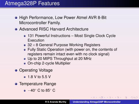
Atmega328P Features
High Performance, Low Power Atmel AVR 8-BitMicrocontroller Family.Advanced RISC Harvard Architecture
131 Powerful Instructions – Most Single Clock CycleExecution32×8 General Purpose Working RegistersFully Static Operation (with power on, the contents ofregisters remain intact even with no clock signal)Up to 20 MIPS Throughput at 20 MHzOn-chip 2-cycle Multiplier
Operating Voltage
1.8 V to 5.5 V
Temperature Range
−40◦ C to 85◦ C
R S Ananda Murthy Understanding Atmega328P Microcontroller

Atmega328P Features
High Endurance Non-volatile Memory Segments
32 K Bytes of In-System Self-Programmable Flash programmemory1 K Bytes EEPROM2 K Bytes Internal SRAMWrite/Erase Cycles: 10,000 Flash/100,000 EEPROMOptional Boot Code Section with Independent Lock BitsProgramming Lock for Software Security
I/O and Packages
23 Programmable I/O Lines28-pin PDIP, 32-lead TQFP, 28-pad QFN/MLF and 32-padQFN/MLF
R S Ananda Murthy Understanding Atmega328P Microcontroller
Atmega328P Features
Peripheral Features
Two 8-bit Timer/Counters with Separate Prescaler andCompare ModeOne 16-bit Timer/Counter with Separate Prescaler,Compare Mode, and Capture ModeReal Time Counter with Separate OscillatorSix PWM Channels8-channel 10-bit ADC in TQFP and QFN/MLF package6-channel 10-bit ADC in PDIP PackageProgrammable Serial USARTMaster/Slave SPI Serial InterfaceByte-oriented 2-wire Serial Interface (Philips I2Ccompatible)Programmable Watchdog Timer with Separate On-chipOscillatorOn-chip Analog ComparatorInterrupt and Wake-up on Pin Change
R S Ananda Murthy Understanding Atmega328P Microcontroller
Atmega328P Features
Special Microcontroller Features
Power-on Reset and Programmable Brown-out DetectionInternal Calibrated OscillatorExternal and Internal Interrupt SourcesSix Sleep Modes: Idle, ADC Noise Reduction, Power-save,Power-down, Standby, and Extended Standby
Speed Grade
0 - 4 MHz @ 1.8 - 5.5V, 0 - 10 MHz @ 2.7 - 5.5 V, 0 -20MHz @ 4.5 - 5.5 V
Power Consumption at 1 MHz, 1.8 V, 25◦C
Active Mode: 0.2mAPower-down Mode: 0.1µAPower-save Mode: 0.75µA (Including 32kHz RTC)
R S Ananda Murthy Understanding Atmega328P Microcontroller
Types of Atmega328P Packages
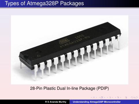
28-Pin Plastic Dual In-line Package (PDIP)
R S Ananda Murthy Understanding Atmega328P Microcontroller
Types of Atmega328P Packages
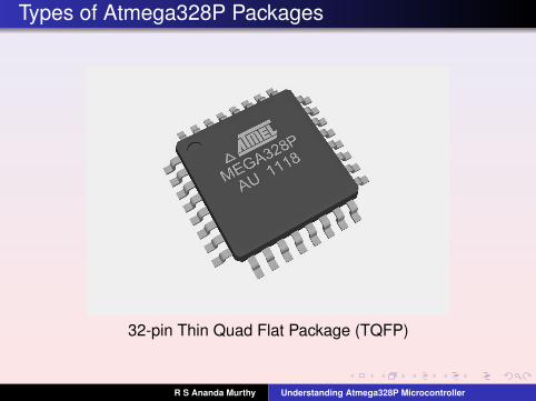
32-pin Thin Quad Flat Package (TQFP)
R S Ananda Murthy Understanding Atmega328P Microcontroller
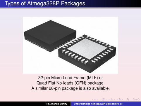
Types of Atmega328P Packages
32-pin Micro Lead Frame (MLF) orQuad Flat No-leads (QFN) package.
A similar 28-pin package is also available.
R S Ananda Murthy Understanding Atmega328P Microcontroller
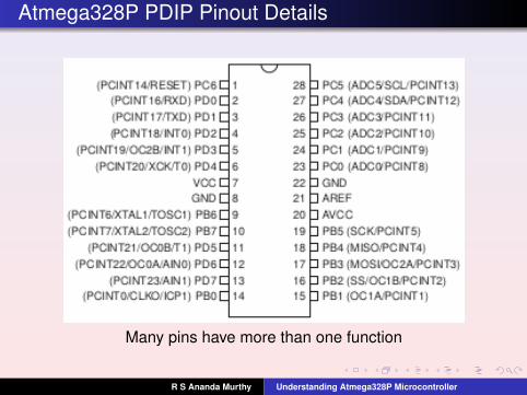
Atmega328P PDIP Pinout Details
Many pins have more than one function
R S Ananda Murthy Understanding Atmega328P Microcontroller
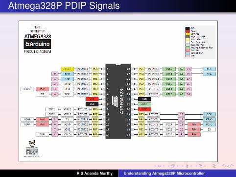
Atmega328P PDIP Signals
R S Ananda Murthy Understanding Atmega328P Microcontroller

Atmega328P 32-TQFP Signals
R S Ananda Murthy Understanding Atmega328P Microcontroller
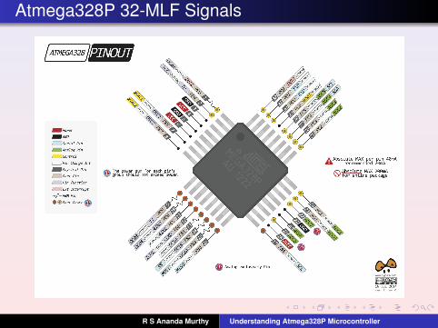
Atmega328P 32-MLF Signals
R S Ananda Murthy Understanding Atmega328P Microcontroller
Pin Descriptions of Atmega328P
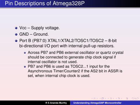
Vcc – Supply voltage.GND – Ground.Port B (PB7:0) XTAL1/XTAL2/TOSC1/TOSC2 – 8-bitbi-directional I/O port with internal pull-up resistors.
Across PB7 and PB6 external oscillator or quartz crystalshould be connected to generate chip clock signal ifinternal oscillator is not used.PB7 and PB6 is used as TOSC2...1 input for theAsynchronous Timer/Counter2 if the AS2 bit in ASSR isset, when internal chip clock is used.
R S Ananda Murthy Understanding Atmega328P Microcontroller
Pin Descriptions of Atmega328P
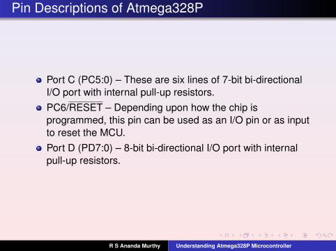
Port C (PC5:0) – These are six lines of 7-bit bi-directionalI/O port with internal pull-up resistors.PC6/RESET – Depending upon how the chip isprogrammed, this pin can be used as an I/O pin or as inputto reset the MCU.Port D (PD7:0) – 8-bit bi-directional I/O port with internalpull-up resistors.
R S Ananda Murthy Understanding Atmega328P Microcontroller
Pin Descriptions of Atmega328P
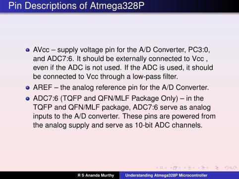
AVcc – supply voltage pin for the A/D Converter, PC3:0,and ADC7:6. It should be externally connected to Vcc ,even if the ADC is not used. If the ADC is used, it shouldbe connected to Vcc through a low-pass filter.AREF – the analog reference pin for the A/D Converter.ADC7:6 (TQFP and QFN/MLF Package Only) – in theTQFP and QFN/MLF package, ADC7:6 serve as analoginputs to the A/D converter. These pins are powered fromthe analog supply and serve as 10-bit ADC channels.
R S Ananda Murthy Understanding Atmega328P Microcontroller
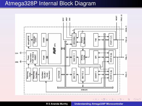
Atmega328P Internal Block Diagram
R S Ananda Murthy Understanding Atmega328P Microcontroller
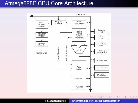
Atmega328P CPU Core Architecture
R S Ananda Murthy Understanding Atmega328P Microcontroller
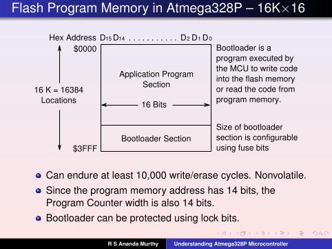
Flash Program Memory in Atmega328P – 16K×16
16 Bits
D15 D14 D0D1D2. . . . . . . . . . .$0000
$3FFF
Application ProgramSection
Bootloader Section
Hex Address
16 K = 16384Locations
Size of bootloadersection is configurableusing fuse bits
Bootloader is aprogram executed bythe MCU to write codeinto the flash memoryor read the code fromprogram memory.
Can endure at least 10,000 write/erase cycles. Nonvolatile.Since the program memory address has 14 bits, theProgram Counter width is also 14 bits.Bootloader can be protected using lock bits.
R S Ananda Murthy Understanding Atmega328P Microcontroller

SRAM Data Memory in Atmega328P – Volatile
32 Registers (GPRs)
D0D1D2. . . . . . . . . . . .
0x0000 - 0x001F
Hex Addresses
64 I/O Registers (SFRs)
D7
160 Ext I/O Registers
0x0020 - 0x005F
2048 x 8 Scratch Pad
0x0060 - 0x00FF
0x0100 - 0x08FF
8 Bits
Stores operands and resultsof arithmetic/logical operations
Used to access peripherals
Used to access extra peripherals
Used to store temporary data
R S Ananda Murthy Understanding Atmega328P Microcontroller
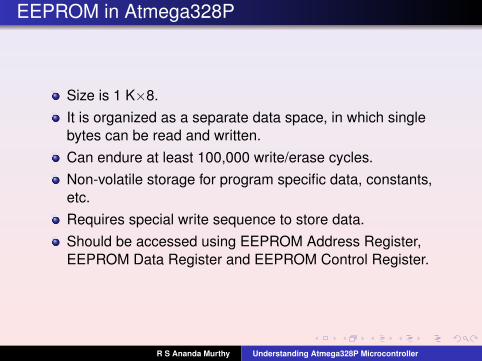
EEPROM in Atmega328P
Size is 1 K×8.It is organized as a separate data space, in which singlebytes can be read and written.Can endure at least 100,000 write/erase cycles.Non-volatile storage for program specific data, constants,etc.Requires special write sequence to store data.Should be accessed using EEPROM Address Register,EEPROM Data Register and EEPROM Control Register.
R S Ananda Murthy Understanding Atmega328P Microcontroller
License
This work is licensed under aCreative Commons Attribution 4.0 International License.
R S Ananda Murthy Understanding Atmega328P Microcontroller
Related Documents