L7: 6.111 Spring 2006 1 Introductory Digital Systems Laboratory L7: Memory Basics and Timing L7: Memory Basics and Timing Acknowledgements: Nathan Ickes J. Rabaey, A. Chandrakasan, B. Nikolic. Digital Integrated Circuits: A Design Perspective. Materials in this lecture are courtesy of the following sources and are used with permission. Prentice Hall/Pearson, 2003. Rex Min Yun Wu

Welcome message from author
This document is posted to help you gain knowledge. Please leave a comment to let me know what you think about it! Share it to your friends and learn new things together.
Transcript

L7: 6.111 Spring 2006 1Introductory Digital Systems Laboratory
L7: Memory Basics and Timing L7: Memory Basics and Timing
Acknowledgements:
Nathan Ickes
J. Rabaey, A. Chandrakasan, B. Nikolic. Digital Integrated Circuits: A Design Perspective.
Materials in this lecture are courtesy of the following sources and are used with permission.
Prentice Hall/Pearson, 2003.
Rex MinYun Wu

L7: 6.111 Spring 2006 2Introductory Digital Systems Laboratory
Memory Classification & MetricsMemory Classification & Metrics
Key Design Metrics:1. Memory Density (number of bits/μm2) and Size2. Access Time (time to read or write) and Throughput 3. Power Dissipation
Read-Write MemoryNon-VolatileRead-Write
MemoryRead-Only Memory (ROM)
EPROM
E2PROM
FLASH
RandomAccess
Non-RandomAccess
SRAM
DRAM
Mask-Programmed
FIFO
LIFO

L7: 6.111 Spring 2006 3Introductory Digital Systems Laboratory
Memory Array ArchitectureMemory Array Architecture
Input-Output(M bits)
2L-K Bit Line
Word Line
Storage Cell
M.2K
Amplify swing torail-to-rail amplitude
Selects appropriate word(i.e., multiplexor)
Sense Amps/Driver
Column DecodeAK-1
A0
Row
Decode
AK
AK+1
AL-1
2L-K row by
Mx2K column cell array

L7: 6.111 Spring 2006 4Introductory Digital Systems Laboratory
Latch and Register Based MemoryLatch and Register Based Memory
Positive Latch Negative Latch
D
G
Q D
G
Q
Clk
DNegative latch
QQM
Positive latch
Register Memory
Works fine for small memory blocks (e.g., small register files)Inefficient in area for large memories – density is the key
metric in large memory circuits
How do we minimize cell size?
1
0
D Q
CLK
0
1
D Q
CLK

L7: 6.111 Spring 2006 5Introductory Digital Systems Laboratory
Static RAM (SRAM) Cell (The 6Static RAM (SRAM) Cell (The 6--T Cell)T Cell)
WL
BL
VDD
M5M6
M4
M1
M2
M3
BL
State held by cross-coupled inverters (M1-M4)Static Memory - retains state as long as power supply turned onFeedback must be overdriven to write into the memory
WL
BLBL
WL
Q Q
Write: set BL and BL to 0 and VDDor VDD and 0 and then enable WL (i.e., set to VDD)Read: Charge BL and BL to VDDand then enable WL (i.e., set to VDD). Sense a small change in BL or BL

L7: 6.111 Spring 2006 6Introductory Digital Systems Laboratory
Tri-state Driver
Interacting with a Memory DeviceInteracting with a Memory Device
Address pins drive row and column decodersData pins are bidirectional and shared by reads and writes
Output Enable gates the chip’s tristate driverWrite Enable sets the memory’s read/write modeChip Enable/Chip Select acts as a “master switch”
Memory Matrix
…
…
Data Pins
ReadLogic
WriteLogic
Row
Decoder
Address Pins
Sense Amps/Drivers
Column Decoder
Write enable
Chip Enable
Output Enable
in out
enable
If enable=0out = Z
If enable =1out = in
Write enable
L7: 6.111 Spring 2006 7Introductory Digital Systems Laboratory
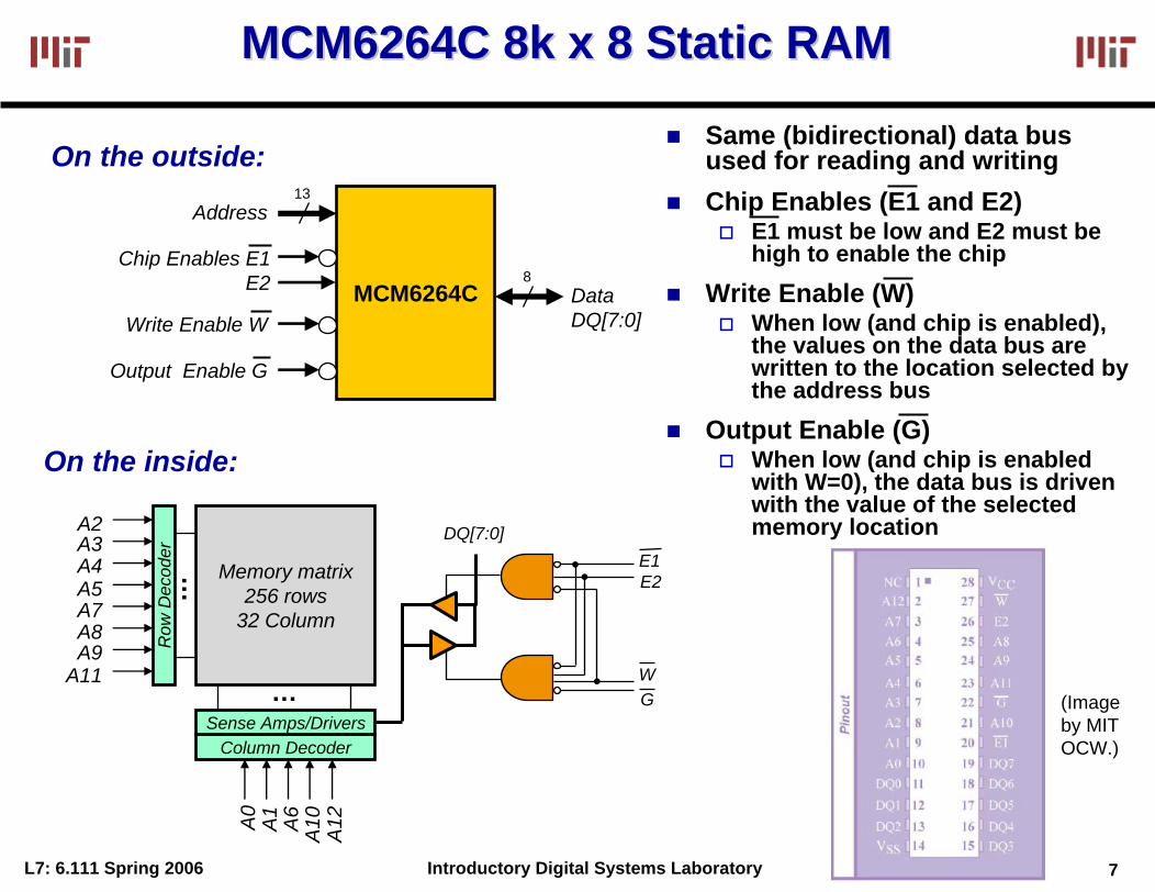
MCM6264C 8k x 8 Static RAMMCM6264C 8k x 8 Static RAM
DQ[7:0]
Memory matrix256 rows
32 Column
Row
Dec
oder
Column DecoderSense Amps/Drivers
…
…
A2A3A4A5A7A8A9
A11
A0
A1
A6
A10 A12
E1E2
WG
MCM6264C
Address
DataDQ[7:0]
13
8Chip Enables E1
E2
Write Enable W
Output Enable G
On the outside:
On the inside:
Same (bidirectional) data bus used for reading and writingChip Enables (E1 and E2)
E1 must be low and E2 must be high to enable the chip
Write Enable (W)When low (and chip is enabled), the values on the data bus are written to the location selected by the address bus
Output Enable (G)When low (and chip is enabled with W=0), the data bus is driven with the value of the selected memory location
(Image by MIT OCW.)

L7: 6.111 Spring 2006 8Introductory Digital Systems Laboratory
Bus tristate time
Reading an Asynchronous SRAMReading an Asynchronous SRAM
Read cycle begins when all enable signals (E1, E2, G) are active Data is valid after read access time
Access time is indicated by full part number: MCM6264CP-12 12ns
Data bus is tristated shortly after G or E1 goes high
Address
E1
G
Data
Address Valid
Data Valid
Access time (from address valid)
Access time (from enable low)
Bus enable time(Tristate)
E2 assumed high (enabled), W =1 (read mode)
L7: 6.111 Spring 2006 9Introductory Digital Systems Laboratory
Bus tristate time
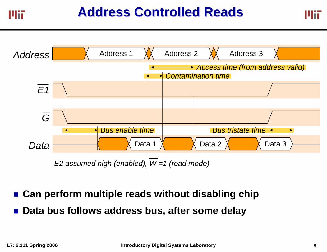
Address Controlled ReadsAddress Controlled Reads
Can perform multiple reads without disabling chipData bus follows address bus, after some delay
Address
E1
G
Data
Access time (from address valid)
Bus enable time
E2 assumed high (enabled), W =1 (read mode)
Address 3Address 2Address 1
Data 2 Data 3Data 1
Contamination time

L7: 6.111 Spring 2006 10Introductory Digital Systems Laboratory
Writing to Asynchronous SRAMWriting to Asynchronous SRAM
Data latched when W or E1 goes high (or E2 goes low)Data must be stable at this timeAddress must be stable before W goes low
Write waveforms are more important than read waveformsGlitches to address can cause writes to random addresses!
Address
E1
W
Data
Address Valid
Address setup time
Write pulse width
Data setup time
E2 and G are held high
Data Valid
Data hold time
Address hold time
L7: 6.111 Spring 2006 11Introductory Digital Systems Laboratory
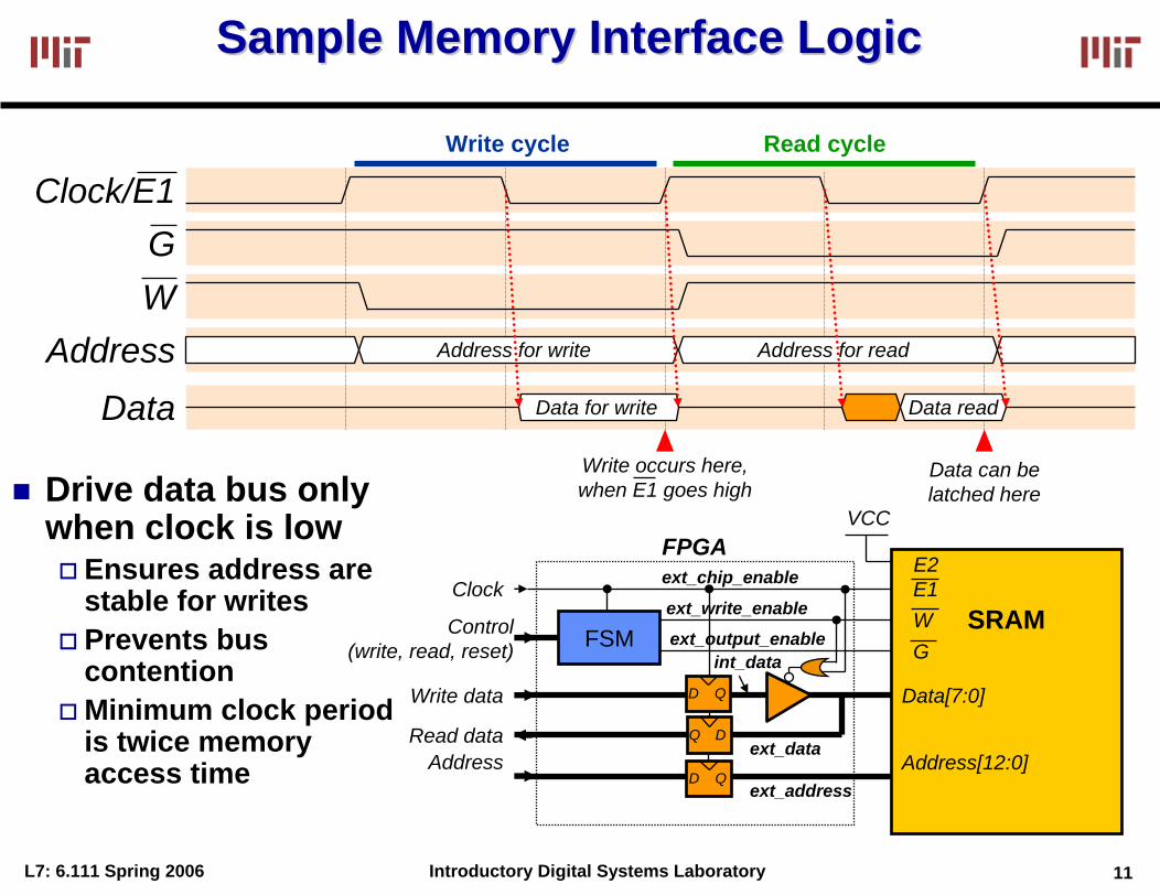
Sample Memory Interface LogicSample Memory Interface Logic
Clock/E1GW
AddressData Data for write
Address for write Address for read
Data read
Write occurs here, when E1 goes high
Data can be latched here
FSM
Clock
DQ
AddressRead data
Write data
Control(write, read, reset)
Drive data bus only when clock is low
Ensures address are stable for writesPrevents bus contentionMinimum clock period is twice memory access time
Write cycle Read cycle
Data[7:0]
Address[12:0]
WG
E1SRAM
E2ext_chip_enable
ext_write_enable
ext_output_enable
ext_address
ext_data
VCC
QD
QD
int_data
FPGA

L7: 6.111 Spring 2006 12Introductory Digital Systems Laboratory
MultiMulti--Cycle Read/Write Cycle Read/Write (less aggressive, recommended timing)(less aggressive, recommended timing)
write states 1-3
write completes
address/data stable
read states 1-3
Data latched into FPGA
read, address is stable
FSM
clk
DQ
address
read_data
write_data
Control(write, read, reset)
Data[7:0]
Address[12:0]
WG
E1
SRAM
E2VDD
W_bG_b
ext_address
ext_data
QD
int_dataQD
data_oen
address_load
data_sample
(Courtesy of Yun Wu. Used with permission.)

L7: 6.111 Spring 2006 13Introductory Digital Systems Laboratory
Simulation from Previous SlideSimulation from Previous Slide
write states 1-3
write completes
address/data stable
read states 1-3
Data latched into FPGA
read, address is stable
(Courtesy of Yun Wu. Used with permission.)

L7: 6.111 Spring 2006 14Introductory Digital Systems Laboratory
module memtest (clk, reset, G_b, W_b, address, ext_address, write_data, read_data, ext_data, read, write, state, data_oen, address_load, data_sample);
input clk, reset, read, write;output G_b, W_b;output [12:0] ext_address;reg [12:0] ext_address;input [12:0] address;input [7:0] write_data;output [7:0] read_data;reg [7:0] read_data;inout [7:0] ext_data;reg [7:0] int_data;output [2:0] state;
reg [2:0] state, next; output data_oen, address_load, data_sample;reg G_b, W_b, G_b_int, W_b_int, address_load,
data_oen, data_oen_int, data_sample;
wire [7:0] ext_data;parameter IDLE = 0;parameter write1 = 1;parameter write2 = 2;parameter write3 = 3;parameter read1 = 4;parameter read2 = 5;parameter read3 = 6;
assign ext_data = data_oen ? int_data : 8'hz;
// Sequential always block for state assignment
always @ (posedge clk)beginif (!reset) state <= IDLE;else state <= next;
G_b <= G_b_int;W_b <= W_b_int;data_oen <= data_oen_int;if (address_load) ext_address <= address;if (data_sample) read_data <= ext_data;if (address_load) int_data <= write_data;end
// note that address_load and data_sample are not// registered signals
2/4
VerilogVerilog for Simple Multifor Simple Multi--Cycle AccessCycle Access
1/4

L7: 6.111 Spring 2006 15Introductory Digital Systems Laboratory
VerilogVerilog for Simple Multifor Simple Multi--Cycle AccessCycle Access
// Combinational always block for next-state // computation
always @ (state or read or write) beginW_b_int = 1; G_b_int = 1;
address_load = 0; data_oen_int = 0; data_sample = 0;case (state)
IDLE: if (write) beginnext = write1;address_load = 1;data_oen_int = 1;end
else if (read) beginnext = read1;address_load = 1;G_b_int = 0;
endelse next = IDLE;
write1: beginnext = write2;W_b_int = 0;data_oen_int =1;end
3/4
write2: beginnext = write3;data_oen_int =1;end
write3: beginnext = IDLE;data_oen_int = 0;end
read1: beginnext = read2;G_b_int = 0;data_sample = 1;end
read2: beginnext = read3;end
read3: beginnext = IDLE;end
default: next = IDLE;endcase
endendmodule
4/4
Setup the Default values

L7: 6.111 Spring 2006 16Introductory Digital Systems Laboratory
Testing MemoriesTesting Memories
Common device problemsBad locations: rare for individual locations to be badSlow (out-of-spec) timing(s): access incorrect data or violates setup/holdCatastrophic device failure: e.g., ESDMissing wire-bonds/devices (!): possible with automated assemblyTransient Failures: Alpha particles, power supply glitch
Common board problemsStuck-at-Faults: a pin shorted to VDD or GNDOpen Circuit Fault: connections unintentionally left outOpen or shorted address wires: causes data to be written to incorrect locationsOpen or shorted control wires: generally renders memory completely inoperable
ApproachDevice problems generally affect the entire chip, almost any test will detect themWriting (and reading back) many different data patterns can detect data bus problemsWriting unique data to every location and then reading it back can detect address bus problems
L7: 6.111 Spring 2006 17Introductory Digital Systems Laboratory
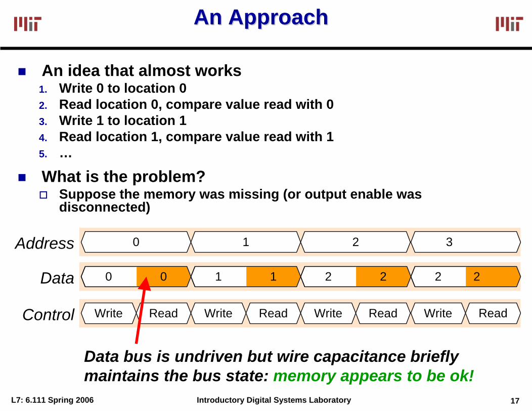
An ApproachAn Approach
An idea that almost works1. Write 0 to location 02. Read location 0, compare value read with 03. Write 1 to location 14. Read location 1, compare value read with 15. …
What is the problem?Suppose the memory was missing (or output enable was disconnected)
Address
Data
Control ReadWriteReadWrite ReadWrite Write
0 1 2 3
0 0 1 1 2 2 2 2
Read
Data bus is undriven but wire capacitance briefly maintains the bus state: memory appears to be ok!

L7: 6.111 Spring 2006 18Introductory Digital Systems Laboratory
A Simple Memory TesterA Simple Memory Tester
Write to all locations, then read back all locations
Separates read/write to the same location with reads/writes of different data to different locations(both data and address busses are changed between read and write to same location)
SRAM
Dat
aA
ddre
ssC
ontr
ol
Counter• Reset counter
• Report failure
• Report success• Read address
<counter>
<counter> = last address?
<counter> = last address?
Does not match?
• Compare data read with 8-LSB’s of <counter>
• Increment counter
Matched?
Comparator
Enable memory
test
To normal memory interface
• Write 0 to address 0• Write 1 to address 1• …• Write (n mod 256) to address n• Read address 0, compare with 0• Read address 1, compare with 1• …• Read address n, compare with (n mod 256)
• write 8-LSB’s of address <counter> to location specified by address <counter>
• Increment counter
L7: 6.111 Spring 2006 19Introductory Digital Systems Laboratory
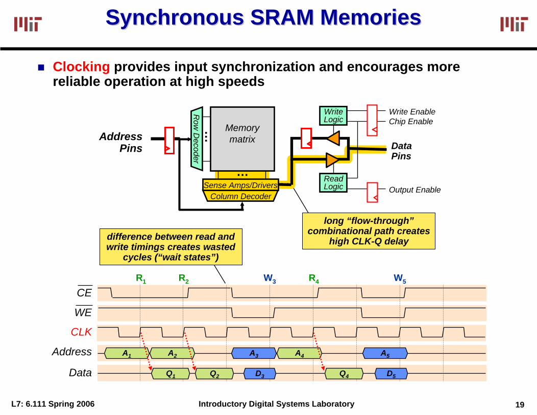
Synchronous SRAM MemoriesSynchronous SRAM Memories
Data Pins
ReadLogic
WriteLogic
Write EnableChip Enable
Output Enable
Clocking provides input synchronization and encourages more reliable operation at high speeds
Memorymatrix
…
…
Row
Decoder
Address Pins
Sense Amps/DriversColumn Decoder
CE
WE
CLK
Address
Data
W3R1
A1
R2 W5R4
A2 A3 A4 A5
Q1 Q2 D3 Q4 D5
difference between read and write timings creates wasted
cycles (“wait states”)
long “flow-through”combinational path creates
high CLK-Q delay

L7: 6.111 Spring 2006 20Introductory Digital Systems Laboratory
ZBT Eliminates the Wait StateZBT Eliminates the Wait State
The wait state occurs because:On a read, data is available after the clock edgeOn a write, data is set up before the clock edge
ZBT (“zero bus turnaround”) memories change the rules for writesOn a write, data is set up after the clock edge (so that it is read on the following edge)Result: no wait states, higher memory throughput
CE
WE
CLK
Address
Data
A1 A2 A3 A4 A5
Q1 Q2 D3 Q4 D5
W3R1 R2 W5R4
Write to A3requested
Data D3loaded
Write to A5requested
Data D5loaded
L7: 6.111 Spring 2006 21Introductory Digital Systems Laboratory
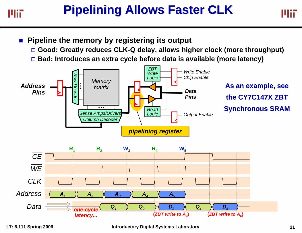
Pipelining Allows Faster CLKPipelining Allows Faster CLK
Pipeline the memory by registering its outputGood: Greatly reduces CLK-Q delay, allows higher clock (more throughput)Bad: Introduces an extra cycle before data is available (more latency)
Data Pins
ReadLogic
Write EnableChip Enable
Output Enable
Memorymatrix
…
…
Row
Decoder
Address Pins
Sense Amps/DriversColumn Decoder
pipelining registerpipelining register
CE
WE
CLK
Address
Data
A1 A2 A3 A4 A5
Q1 Q2 D3 Q4 D5
W3R1 R2 W5R4
one-cyclelatency... (ZBT write to A3) (ZBT write to A5)
ZBTWriteLogic
As an example, see As an example, see the CY7C147X ZBT the CY7C147X ZBT
Synchronous SRAMSynchronous SRAM

L7: 6.111 Spring 2006 22Introductory Digital Systems Laboratory
EPROM Cell EPROM Cell –– The Floating Gate TransistorThe Floating Gate Transistor
This is a non-volatile memory (retains state when supply turned off)
EPROM CellImage removed due to copyright restrictions.
Removing programming voltage leaves charge trapped
0 V
5 V 0 V
DS
5 V
2.5 V 5 V
DS
Programming results inhigher VT.
20 V
10 V 5 V 20 V
DS
Avalanche injection
[Rabaey03]

L7: 6.111 Spring 2006 23Introductory Digital Systems Laboratory
Interacting with Flash and (E)EPROMInteracting with Flash and (E)EPROM
Reading from flash or (E)EPROM is the same as reading from SRAMVpp: input for programming voltage (12V)
EPROM: Vpp is supplied by programming machineModern flash/EEPROM devices generate 12V using an on-chip charge pump
EPROM lacks a write enableNot in-system programmable (must use a special programming machine)
For flash and EEPROM, write sequence is controlled by an internal FSMWrites to device are used to send signals to the FSMAlthough the same signals are used, one can’t write to flash/EEPROM in the same manner as SRAM
Address Data
Chip Enable
Output Enable
Write Enable FSM
Vcc (5V)
Programming voltage (12V)
Charge pump
Flash/EEPROM block diagram
EPROM omits FSM, charge
pump, and write enable

L7: 6.111 Spring 2006 24Introductory Digital Systems Laboratory
Dynamic RAM (DRAM) CellDynamic RAM (DRAM) Cell
DRAM relies on charge stored in a capacitor to hold stateFound in all high density memories (one bit/transistor)Must be “refreshed” or state will be lost – high overhead
DRAM uses Special
Capacitor Structures
To Write: set Bit Line (BL) to 0 or VDD& enable Word Line (WL) (i.e., set to VDD )To Read: set Bit Line (BL) to VDD /2& enable Word Line (i.e., set it to VDD ) Image by Wikipedia user Cyferz.
WL
X
BLVDD/2
VDD
GND
Write "1" Read "1"
sensingVDD/2
[Rabaey03]
CSM1
BLWL
CBL

L7: 6.111 Spring 2006 25Introductory Digital Systems Laboratory
Asynchronous DRAM OperationAsynchronous DRAM Operation
Clever manipulation of RAS and CAS after reads/writes provide more efficient modes: early-write, read-write, hidden-refresh, etc.(See datasheets for details)
Address
RAS
CAS
Data
WE
Row
Q (data from RAM)
Col
RAS-before-CAS for a read or write
(Row and column addresses taken on falling edges of RAS and CAS)
(Tristate)
CAS-before-RAS for a refresh
set high/low before asserting CAS

L7: 6.111 Spring 2006 26Introductory Digital Systems Laboratory
Addressing with Memory MapsAddressing with Memory Maps
‘138 is a 3-to-8 decoderMaps 16-bit address space to 8, 13-bit segmentsUpper 3-bits of address determine which chip is enabled
SRAM-like interface is often used for peripherals
Referred to as “memory mapped” peripherals
Dat
a[7:
0]A
ddre
ss[1
2:0]
~W~G ~E1
SRAM 1
‘138
Y7Y6Y5Y4Y3Y2Y1Y0
C
BA
~G2B~G2A
G1
Dat
a[7:
0]A
ddre
ss[1
2:0]
~W~G ~E1
SRAM 2
Dat
a[7:
0]A
ddre
ss[1
2:0]
~G ~E1
EPROM
[12:
0]
[12:
0]
[12:
0]
131415
Address[15:0]
Write EnableOutput Enable
Data[7:0]
Dat
a[7:
0]A
ddre
ss[2
:0]
~W~G ~E1
ADC
EPROMSRAM 2SRAM 1
0xFFFF
0xE0000xDFFF
0xC0000xBFFF
0xA0000x9FFF
0x0000
[2:0
]
ADC0x20000x1FFF
Memory Map
Bus Enable
+5V
Analog Input

L7: 6.111 Spring 2006 27Introductory Digital Systems Laboratory
Key Messages on Memory DevicesKey Messages on Memory Devices
SRAM vs. DRAMSRAM holds state as long as power supply is turned on. DRAM must be “refreshed” – results in more complicated controlDRAM has much higher density, but requires special capacitor technology. FPGA usually implemented in a standard digital process technology and uses SRAM technology
Non-Volatile MemoryFast Read, but very slow write (EPROM must be removed from the system for programming!)Holds state even if the power supply is turned off
Memory InternalsHas quite a bit of analog circuits internally -- pay particular attention to noise and PCB board integration
Device detailsDon’t worry about them, wait until 6.012 or 6.374
L7: 6.111 Spring 2006 28Introductory Digital Systems Laboratory
You Should Understand WhyYou Should Understand Why……
control signals such as Write Enable should be registereda multi-cycle read/write is safer from a timing perspective than the single cycle read/write approachit is a bad idea to enable two tri-states driving the bus at the same timean SRAM does not need to be “refreshed” while a DRAM doesan EPROM/EEPROM/FLASH cell can hold its state even if the power supply is turned offa synchronous memory can result in higher throughput