L306 Hardware Design Copyright © Shanghai Mobiletek Communication Ltd 0 L306 Hardware Design GSM/WCDMA Module Series Version: V1.3 Date: 2016-11-10 Shanghai Mobiletek Communication Ltd

Welcome message from author
This document is posted to help you gain knowledge. Please leave a comment to let me know what you think about it! Share it to your friends and learn new things together.
Transcript
L306 Hardware Design
Copyright © Shanghai Mobiletek Communication Ltd 0
L306 Hardware Design
GSM/WCDMA Module Series
Version: V1.3
Date: 2016-11-10
Shanghai Mobiletek Communication Ltd

L306 Hardware Design
Copyright © Shanghai Mobiletek Communication Ltd 1
Notice
Some features of the product and its accessories described herein rely on the software installed,
capacities and settings of local network, and therefore may not be activated or may be limited by local
network operators or network service providers. Thus, the descriptions herein may not exactly match
the product or its accessories which you purchase. Shanghai Mobiletek Communication Ltd reserves
the right to change or modify any information or specifications contained in this manual without prior
notice and without any liability.
Copyright
This document contains proprietary technical information which is the property of Shanghai Mobiletek
Communication Ltd. copying of this document and giving it to others and the using or communication
of the contents thereof, are forbidden without express authority. Offenders are liable to the payment of
damages. All rights reserved in the event of grant of patent or the registration of a utility model or
design. All specification supplied herein are subject to change without notice at any time.
DISCLAIMER
ALL CONTENTS OF THIS MANUAL ARE PROVIDED “AS IS”. EXCEPT AS REQUIRED BY
APPLICABLE LAWS, NO WARRANTIES OF ANY KIND, EITHER EXPRESS OR IMPLIED,
INCLUDINGBUT NOT LIMITED TO, THE IMPLIED WARRANTIES OF MERCHANTABILITY AND
FITNESS FOR A PARTICULAR PURPOSE, ARE MADE IN RELATION TO THE ACCURACY,
RELIABILITY OR CONTENTS OF THIS MANUAL.TO THE MAXIMUM EXTENT PERMITTED BY
APPLICABLE LAW, IN NO EVENT SHALL SHANGHAI MOBILETEKCOMMUNICATION LTD BE
LIABLE FOR ANY SPECIAL, INCIDENTAL, INDIRECT, OR CONSEQUENTIAL DAMAGES, OR
LOSS OF PROFITS, BUSINESS, REVENUE, DATA, GOODWILL SAVINGS OR ANTICIPATED
SAVINGS REGARDLESS OF WHETHER SUCH LOSSES ARE FORSEEABLE OR NOT.
LYNQ
CONDENTIAL
L306 Hardware Design
Copyright © Shanghai Mobiletek Communication Ltd 2
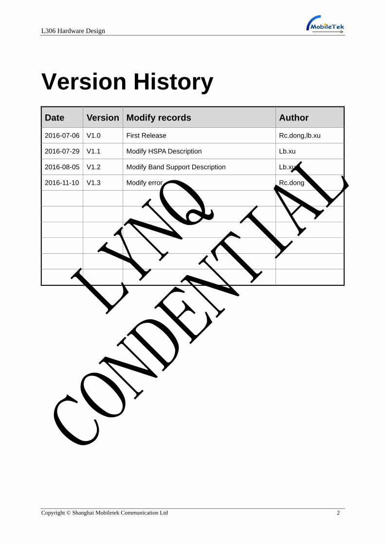
Version History
Date Version Modify records Author
2016-07-06 V1.0 First Release Rc.dong,lb.xu
2016-07-29 V1.1 Modify HSPA Description Lb.xu
2016-08-05 V1.2 Modify Band Support Description Lb.xu
2016-11-10 V1.3 Modify error Rc.dong
LYNQ
CONDENTIAL

L306 Hardware Design
Copyright © Shanghai Mobiletek Communication Ltd 3
CONTENT
1. INTRODUCTION .......................................................................................................................................... 5
1.1 HARDWARE DIAGRAM .............................................................................................................................................. 5
1.2 MAIN FEATURES ....................................................................................................................................................... 5
1.3 SPECIFICATIONS ....................................................................................................................................................... 6
1.4 INTERFACES ............................................................................................................................................................. 7
2. PACKAGE INFORMATION ............................................................................................................................ 8
2.1 PIN CONFIGURATION ................................................................................................................................................ 8
2.2 PIN DEFINITION ........................................................................................................................................................ 8
2.3 PACKAGE INFORMATION .......................................................................................................................................... 13
2.3.1 Dimensions ................................................................................................................................................ 13
2.3.2 Module size ................................................................................................................................................ 14
2.3.3 Recommend Pad ........................................................................................................................................ 16
3. INTERFACE CIRCUIT DESIGN ...................................................................................................................... 18
3.1 POWER SECTION .................................................................................................................................................... 18
3.1.1 Power Supply ............................................................................................................................................. 18
3.1.2 Power pin description ................................................................................................................................ 19
3.1.3 Hardware Power on ................................................................................................................................... 19
3.1.4 Hardware reset .......................................................................................................................................... 19
3.2 USIM INTERFACE ................................................................................................................................................... 20
3.2.1 Pin Description ........................................................................................................................................... 20
3.2.2 USIM application ....................................................................................................................................... 20
3.3 TF CARD INTERFACE ............................................................................................................................................... 21
3.4 USB INTERFACE ..................................................................................................................................................... 22
3.5 PCM INTERFACE .................................................................................................................................................... 23
3.6 IIC INTERFACE ....................................................................................................................................................... 24
3.7 SPI INTERFACE ...................................................................................................................................................... 24
3.8 UART INTERFACE ................................................................................................................................................... 25
3.8.1 Pin Description ........................................................................................................................................... 25
3.8.2 UART application ....................................................................................................................................... 26
3.9 INTERACTIVE APPLICATION INTERFACE ........................................................................................................................ 28
3.10 LED INTERFACE ................................................................................................................................................... 29
3.10.1 LED Control circuit ................................................................................................................................... 29
3.10.2 LED State description ............................................................................................................................... 29
4. ELECTRICAL CHARACTERISTICS .................................................................................................................. 31
4.1 ELECTRICAL CHARACTERISTICS ................................................................................................................................... 31
4.2 TEMPERATURE CHARACTERISTIC ................................................................................................................................ 31
4.3 ABSOLUTE MAXIMUM POWER.................................................................................................................................. 32
4.4 RECOMMENDED OPERATING CONDITIONS ................................................................................................................... 32
4.5 POWER SEQUENCE ................................................................................................................................................. 33
LYNQ
CONDENTIAL
L306 Hardware Design
Copyright © Shanghai Mobiletek Communication Ltd 4
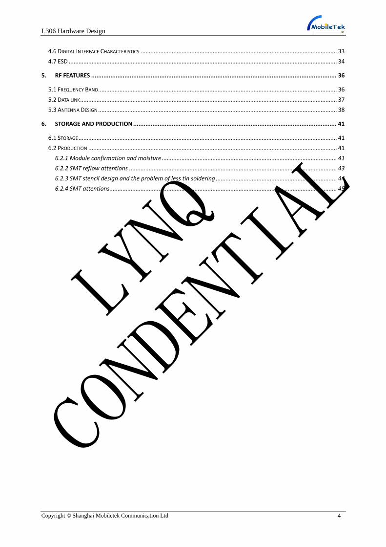
4.6 DIGITAL INTERFACE CHARACTERISTICS ........................................................................................................................ 33
4.7 ESD .................................................................................................................................................................... 34
5. RF FEATURES ............................................................................................................................................ 36
5.1 FREQUENCY BAND .................................................................................................................................................. 36
5.2 DATA LINK ............................................................................................................................................................. 37
5.3 ANTENNA DESIGN .................................................................................................................................................. 38
6. STORAGE AND PRODUCTION .................................................................................................................... 41
6.1 STORAGE .............................................................................................................................................................. 41
6.2 PRODUCTION ........................................................................................................................................................ 41
6.2.1 Module confirmation and moisture ........................................................................................................... 41
6.2.2 SMT reflow attentions ............................................................................................................................... 43
6.2.3 SMT stencil design and the problem of less tin soldering .......................................................................... 44
6.2.4 SMT attentions ........................................................................................................................................... 45
LYNQ
CONDENTIAL
L306 Hardware Design
Copyright © Shanghai Mobiletek Communication Ltd 5
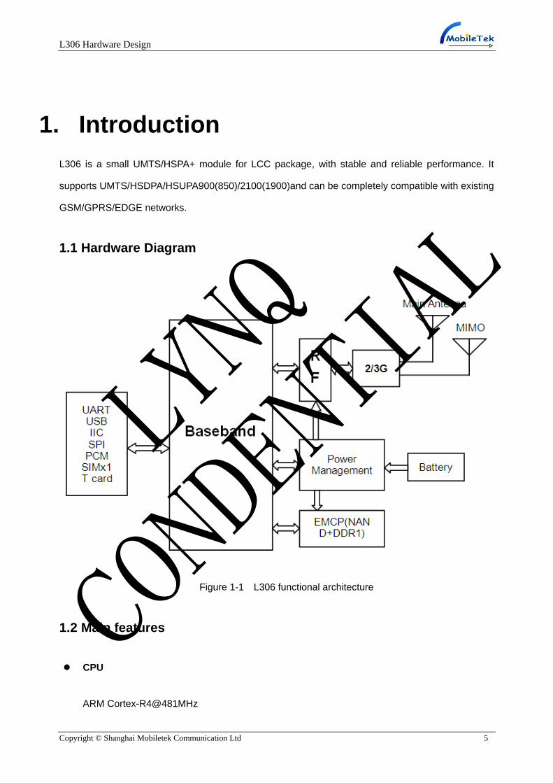
1. Introduction
L306 is a small UMTS/HSPA+ module for LCC package, with stable and reliable performance. It
supports UMTS/HSDPA/HSUPA900(850)/2100(1900)and can be completely compatible with existing
GSM/GPRS/EDGE networks.
1.1 Hardware Diagram
Figure 1-1 L306 functional architecture
1.2 Main features
CPU
ARM Cortex-R4@481MHz
LYNQ
CONDENTIAL
L306 Hardware Design
Copyright © Shanghai Mobiletek Communication Ltd 6
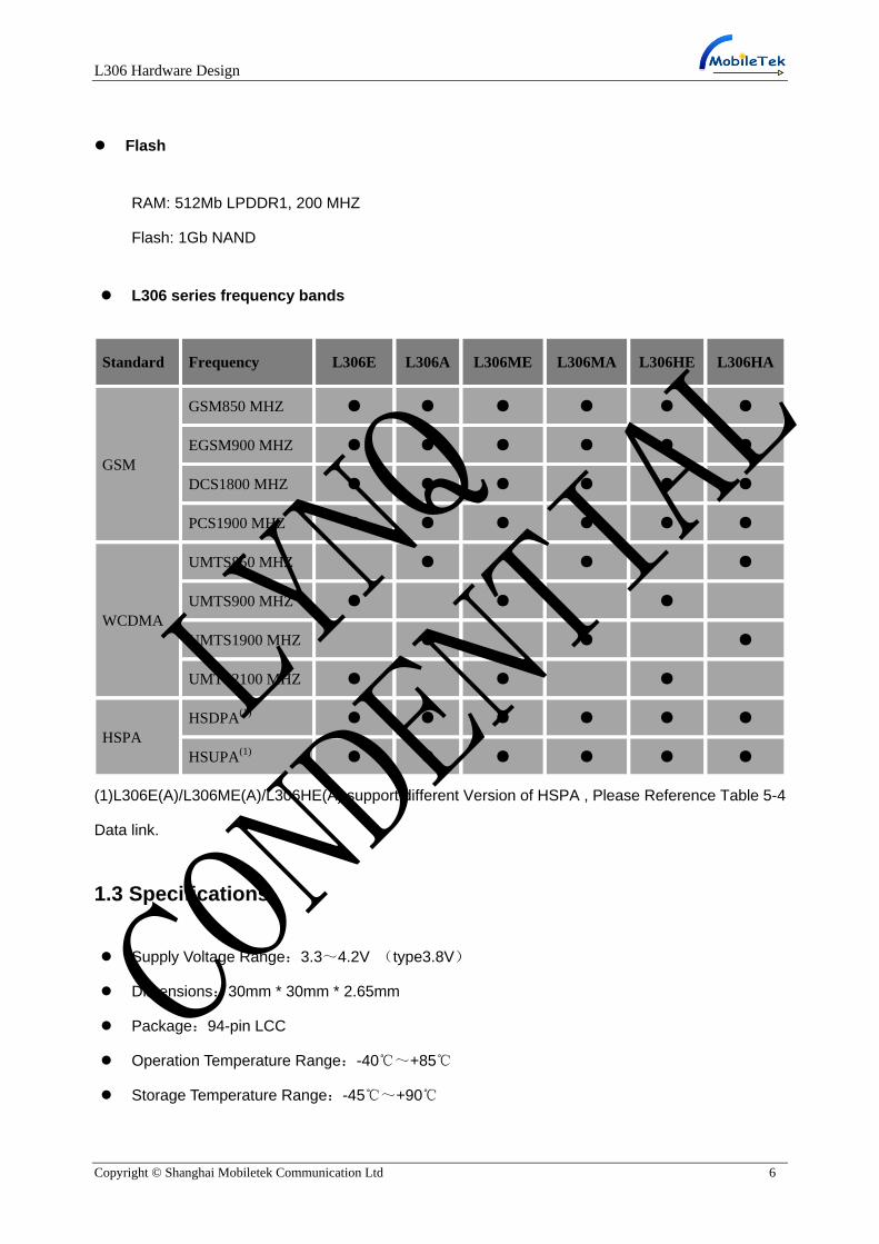
Flash
RAM: 512Mb LPDDR1, 200 MHZ
Flash: 1Gb NAND
L306 series frequency bands
Standard Frequency L306E L306A L306ME L306MA L306HE L306HA
GSM
GSM850 MHZ ● ● ● ● ● ●
EGSM900 MHZ ● ● ● ● ● ●
DCS1800 MHZ ● ● ● ● ● ●
PCS1900 MHZ ● ● ● ● ● ●
WCDMA
UMTS850 MHZ ● ● ●
UMTS900 MHZ ● ● ●
UMTS1900 MHZ ● ● ●
UMTS2100 MHZ ● ● ●
HSPA
HSDPA(1)
● ● ● ● ● ●
HSUPA(1)
● ● ● ● ● ●
(1)L306E(A)/L306ME(A)/L306HE(A) support different Version of HSPA , Please Reference Table 5-4
Data link.
1.3 Specifications
Supply Voltage Range:3.3~4.2V (type3.8V)
Dimensions:30mm * 30mm * 2.65mm
Package:94-pin LCC
Operation Temperature Range:-40℃~+85℃
Storage Temperature Range:-45℃~+90℃
LYNQ
CONDENTIAL
L306 Hardware Design
Copyright © Shanghai Mobiletek Communication Ltd 7
Antenna:Main Antenna、Diversity Antenna
Weight :Approx 5g
1.4 Interfaces
SDIO
SPI
IIC
PCM: Digital audio interface
SIM: Support 1.8V/3V
UART: High speed UART
USB 2.0: High Speed ,480Mbps
LYNQ
CONDENTIAL
L306 Hardware Design
Copyright © Shanghai Mobiletek Communication Ltd 8
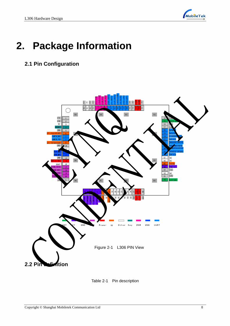
2. Package Information
2.1 Pin Configuration
Figure 2-1 L306 PIN View
2.2 Pin definition
Table 2-1 Pin description
LYNQ
CONDENTIAL
L306 Hardware Design
Copyright © Shanghai Mobiletek Communication Ltd 9
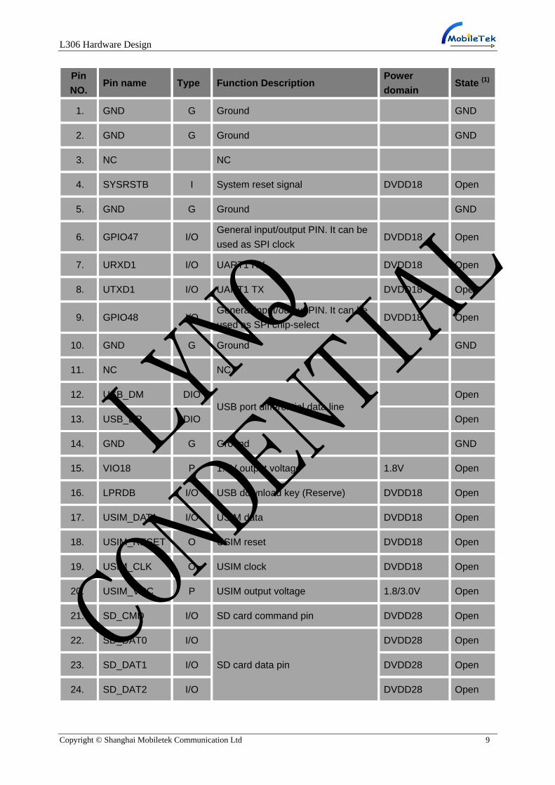
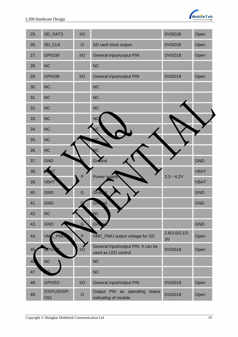
Pin
NO. Pin name Type Function Description
Power
domain State
(1)
1. GND G Ground GND
2. GND G Ground GND
3. NC NC
4. SYSRSTB I System reset signal DVDD18 Open
5. GND G Ground GND
6. GPIO47 I/O General input/output PIN. It can be
used as SPI clock DVDD18 Open
7. URXD1 I/O UART1 RX DVDD18 Open
8. UTXD1 I/O UART1 TX DVDD18 Open
9. GPIO48 I/O General input/output PIN. It can be
used as SPI chip-select DVDD18 Open
10. GND G Ground GND
11. NC NC
12. USB_DM DIO
USB port differential data line
Open
13. USB_DP DIO Open
14. GND G Ground GND
15. VIO18 P 1.8V output voltage 1.8V Open
16. LPRDB I/O USB download key (Reserve) DVDD18 Open
17. USIM_DATA I/O USIM data DVDD18 Open
18. USIM_RESET O USIM reset DVDD18 Open
19. USIM_CLK O USIM clock DVDD18 Open
20. USIM_VCC P USIM output voltage 1.8/3.0V Open
21. SD_CMD I/O SD card command pin DVDD28 Open
22. SD_DAT0 I/O
SD card data pin
DVDD28 Open
23. SD_DAT1 I/O DVDD28 Open
24. SD_DAT2 I/O DVDD28 Open
LYNQ
CONDENTIAL
L306 Hardware Design
Copyright © Shanghai Mobiletek Communication Ltd 10
25. SD_DAT3 I/O DVDD28 Open
26. SD_CLK O SD card clock output DVDD28 Open
27. GPIO39 I/O General input/output PIN DVDD18 Open
28. NC NC
29. GPIO38 I/O General input/output PIN DVDD18 Open
30. NC NC
31. NC NC
32. NC NC
33. NC NC
34. NC NC
35. NC NC
36. NC NC
37. GND G Ground GND
38. VBAT
P Power supply 3.3~4.2V
VBAT
39. VBAT VBAT
40. GND G Ground GND
41. GND G Ground GND
42. NC NC
43. GND G Ground GND
44. VMC_PMU P VMC_PMU output voltage for SD 2.8/3.0/3.1/3.
3V Open
45. GPIO17 I/O General input/output PIN. It can be
used as LED control DVDD18 Open
46. NC NC
47. NC NC
48. GPIO53 I/O General input/output PIN DVDD18 Open
49. STATUS/GPI
O51 O
Output PIN as operating status
indicating of module DVDD18 Open
LYNQ
CONDENTIAL
L306 Hardware Design
Copyright © Shanghai Mobiletek Communication Ltd 11
50. WAKEUP
IN/GPIO0 I/O
Host to set the module into sleep or
wake up the module from sleep DVDD18 Open
51. NETLIGHT/G
PIO54 O
Output PIN as LED control for
network status DVDD18 Open
52. WAKEOUT/G
PIO46 I/O
General input/output PIN. It can be
used as wake signal to host from
module
DVDD18 Open
53. GPIO52 I/O General input/output PIN DVDD18 Open
54. FLIGHTMOD
E/ GPIO1 I Input PIN as RF operating control DVDD18 Open
55. GPIO44 I/O General input/output PIN. It can be
used as IIC clock DVDD18 Open
56. GPIO49 I/O General input/output PIN. It can be
used as IIC data DVDD18 Open
57. GND G Ground GND
58. GND G Ground GND
59. MAIN_ANT ANT RF Main Antenna Open
60. GND G Ground GND
61. GND G Ground GND
62. VBAT
P Power supply 3.3~4.2V
VBAT
63. VBAT VBAT
64. GND G Ground GND
65. GND G Ground GND
66. UART0_RTS DO UART0 ready to receive DVDD18 Open
67. UART0_CTS DI UART0 clear to send DVDD18 Open
68. UART0_RX DI UART0 receive data input DVDD18 Open
69. UART0_RING DO UART0 ring indicator DVDD18 Open
70. UART0_DCD DO UART0 data carrier detect DVDD18 Open
71. UART0_TX DO UART0 transmit output DVDD18 Open
72. UART0_DTR DI UART0 Data terminal ready DVDD18 Open
73. PCM_DOUT I/O PCM I/F data out DVDD18 Open
LYNQ
CONDENTIAL

L306 Hardware Design
Copyright © Shanghai Mobiletek Communication Ltd 12
74. PCM_DIN I/O PCM I/F data in DVDD18 Open
75. PCM_SYNC I/O PCM interface sync DVDD18 Open
76. PCM_CLK I/O PCM interface clock DVDD18 Open
77. GND G Ground GND
78. GND G Ground GND
79. NC NC
80. GND G Ground GND
81. GND G Ground GND
82. AUX_ANT ANT MIMO Antenna Open
83. GND G Ground GND
84. GND G Ground GND
85. GND G Ground GND
86. GND G Ground GND
87. GND G Ground GND
88. GND G Ground GND
89. GND G Ground GND
90. GND G Ground GND
91. GND G Ground GND
92. GND G Ground GND
93. GND G Ground GND
94. GND G Ground GND
(1) Suggested status when not in use.
Table 2-2 Pin type description
P:POWER G:GROUND
I:INPUT DI:DIGITAL INPUT
LYNQ
CONDENTIAL
L306 Hardware Design
Copyright © Shanghai Mobiletek Communication Ltd 13
O:OUTPUT DO:DIGITAL OUTPUT
ANT:ANTENNA DIO:DIGITAL INPUT OUTPUT
NC:NOT CONNECT
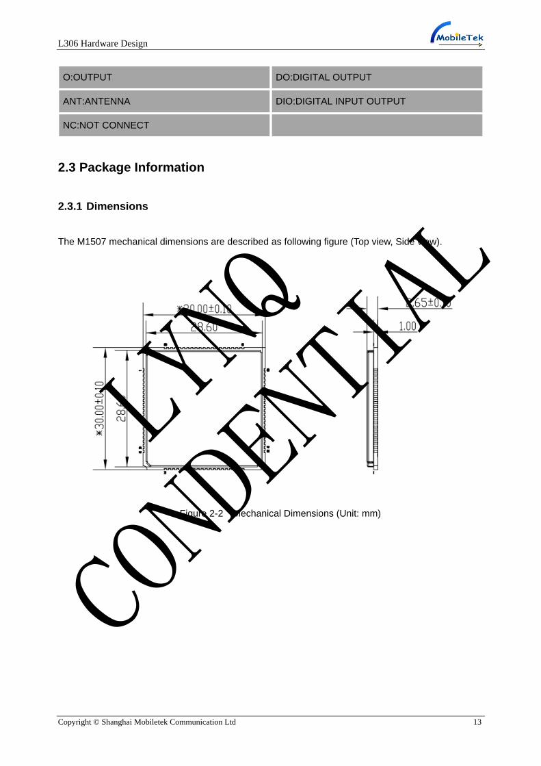
2.3 Package Information
2.3.1 Dimensions
The M1507 mechanical dimensions are described as following figure (Top view, Side view).
Figure 2-2 Mechanical Dimensions (Unit: mm) LYNQ
CONDENTIAL
L306 Hardware Design
Copyright © Shanghai Mobiletek Communication Ltd 14
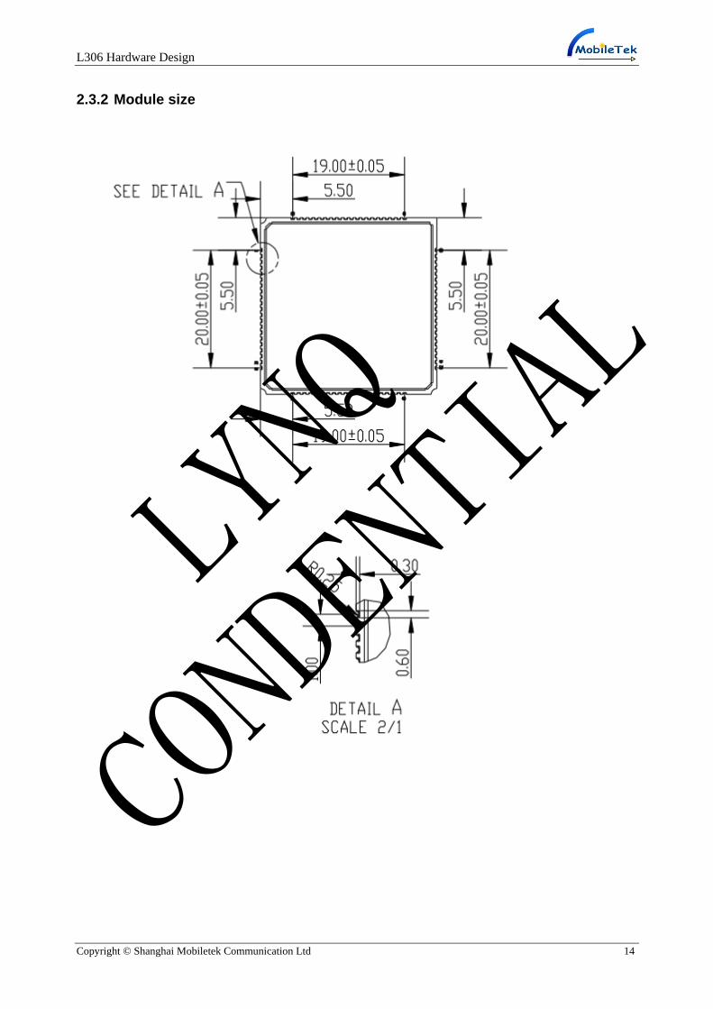
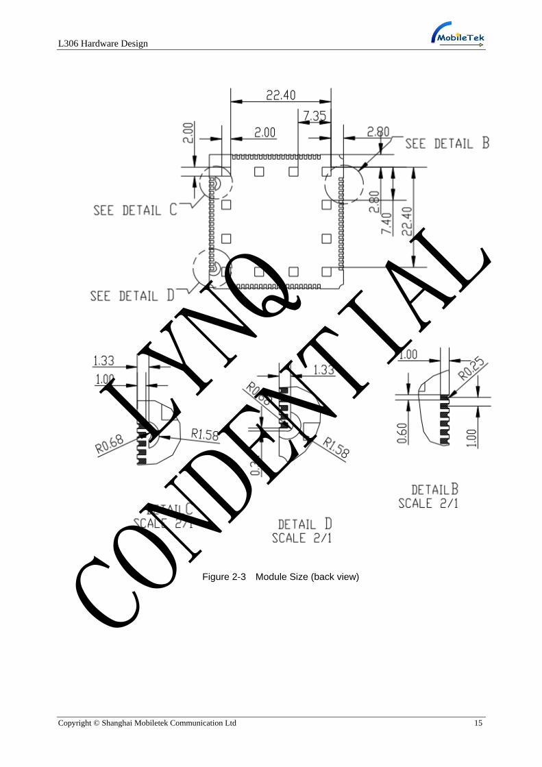
2.3.2 Module size
LYNQ
CONDENTIAL
L306 Hardware Design
Copyright © Shanghai Mobiletek Communication Ltd 15
Figure 2-3 Module Size (back view)
LYNQ
CONDENTIAL
L306 Hardware Design
Copyright © Shanghai Mobiletek Communication Ltd 16
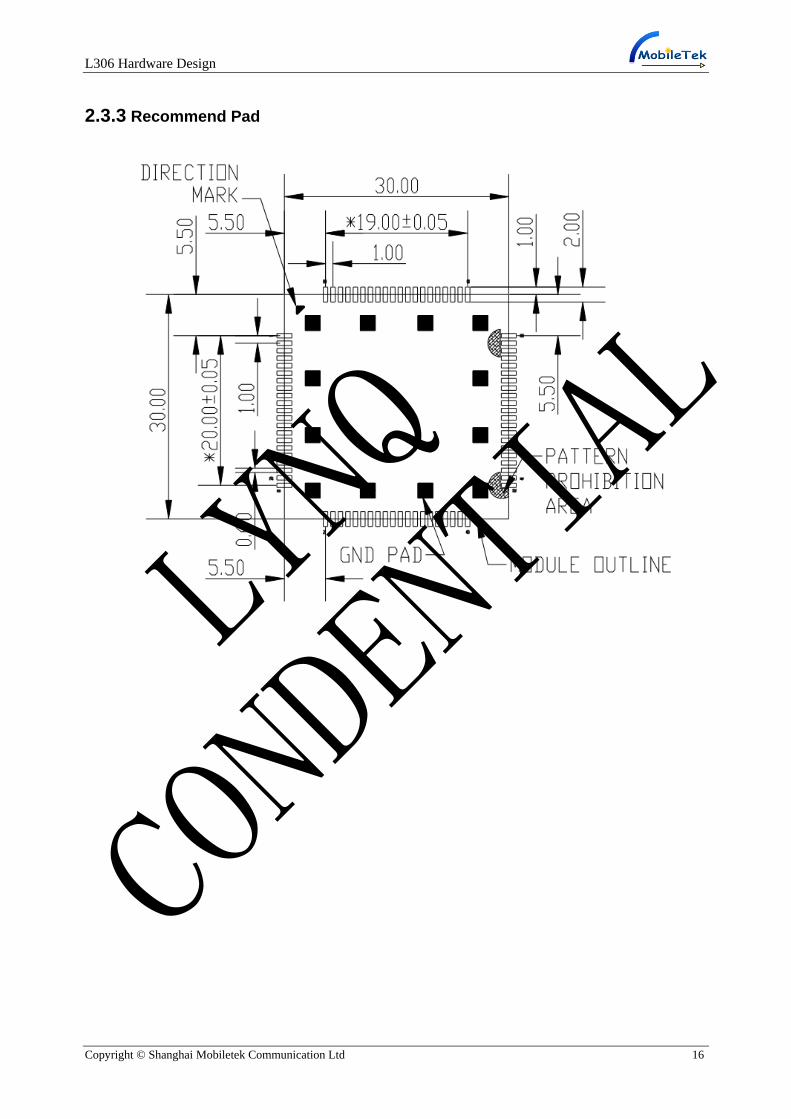
2.3.3 Recommend Pad
LYNQ
CONDENTIAL
L306 Hardware Design
Copyright © Shanghai Mobiletek Communication Ltd 17
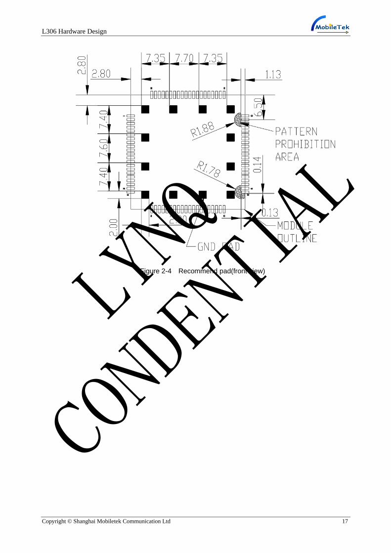
Figure 2-4 Recommend pad(front view)
LYNQ
CONDENTIAL
L306 Hardware Design
Copyright © Shanghai Mobiletek Communication Ltd 18
3. Interface Circuit Design
3.1 Power Section
3.1.1 Power Supply
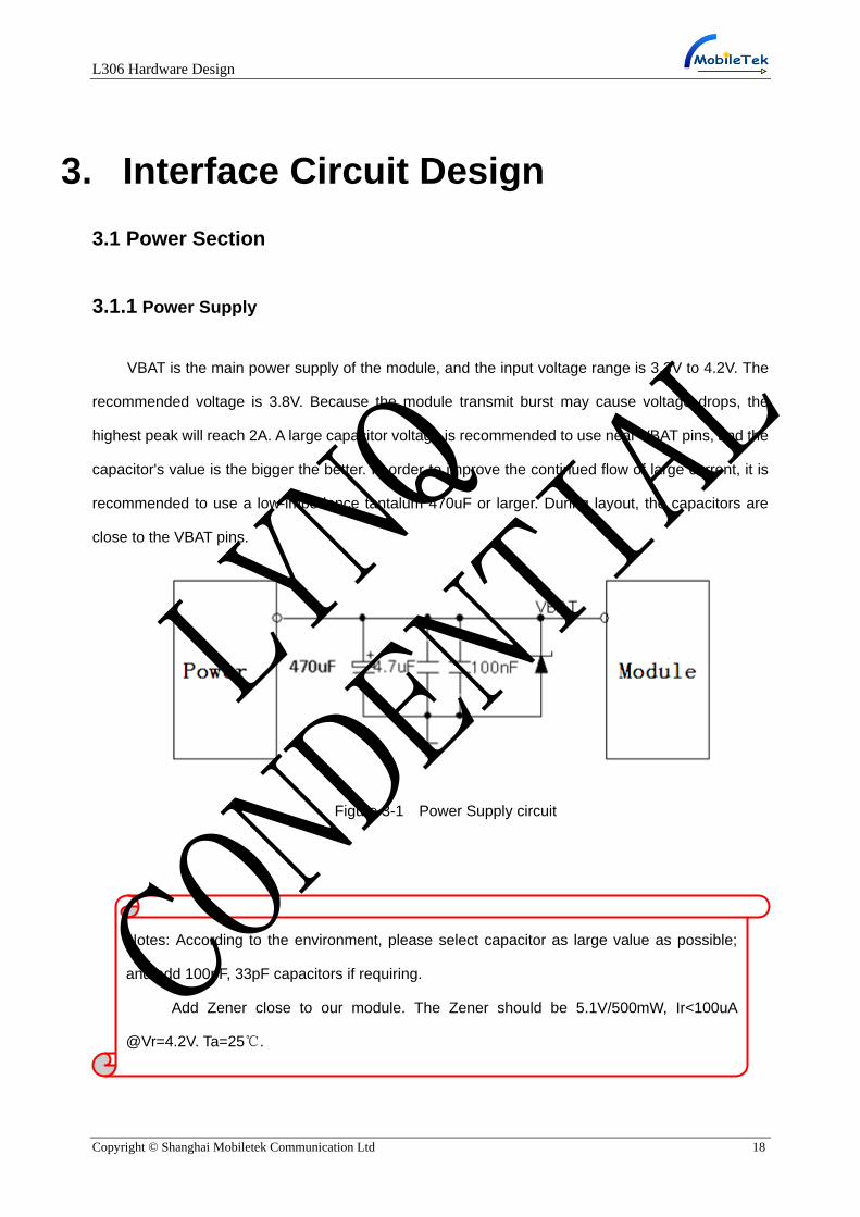
VBAT is the main power supply of the module, and the input voltage range is 3.3V to 4.2V. The
recommended voltage is 3.8V. Because the module transmit burst may cause voltage drops, the
highest peak will reach 2A. A large capacitor voltage is recommended to use near VBAT pins, and the
capacitor's value is the bigger the better. In order to improve the continued flow of large current, it is
recommended to use a low-impedance tantalum 470uF or larger. During layout, the capacitors are
close to the VBAT pins.
Figure 3-1 Power Supply circuit
Notes: According to the environment, please select capacitor as large value as possible;
and add 100pF, 33pF capacitors if requiring.
Add Zener close to our module. The Zener should be 5.1V/500mW, Ir<100uA
@Vr=4.2V. Ta=25℃.
LYNQ
CONDENTIAL
L306 Hardware Design
Copyright © Shanghai Mobiletek Communication Ltd 19
3.1.2 Power pin description
Pin number Pin name Description
38/39/62/63 VBAT positive signal
1/2/5/10/14/37/40/41/43/57/58/60/64/65
77/78/80/81 GND GND
83/84/85/86/87/88/89/90/91/92/93/94 GND GND
The Ground of power and signal need to be GND signal connection is not complete will have an
impact on the performance of the product. In addition, there are a total of 12 (83~94) heat sink and
fixed pad.
3.1.3 Hardware Power on
L306 module does not have a separate boot key, using the power on the boot form.
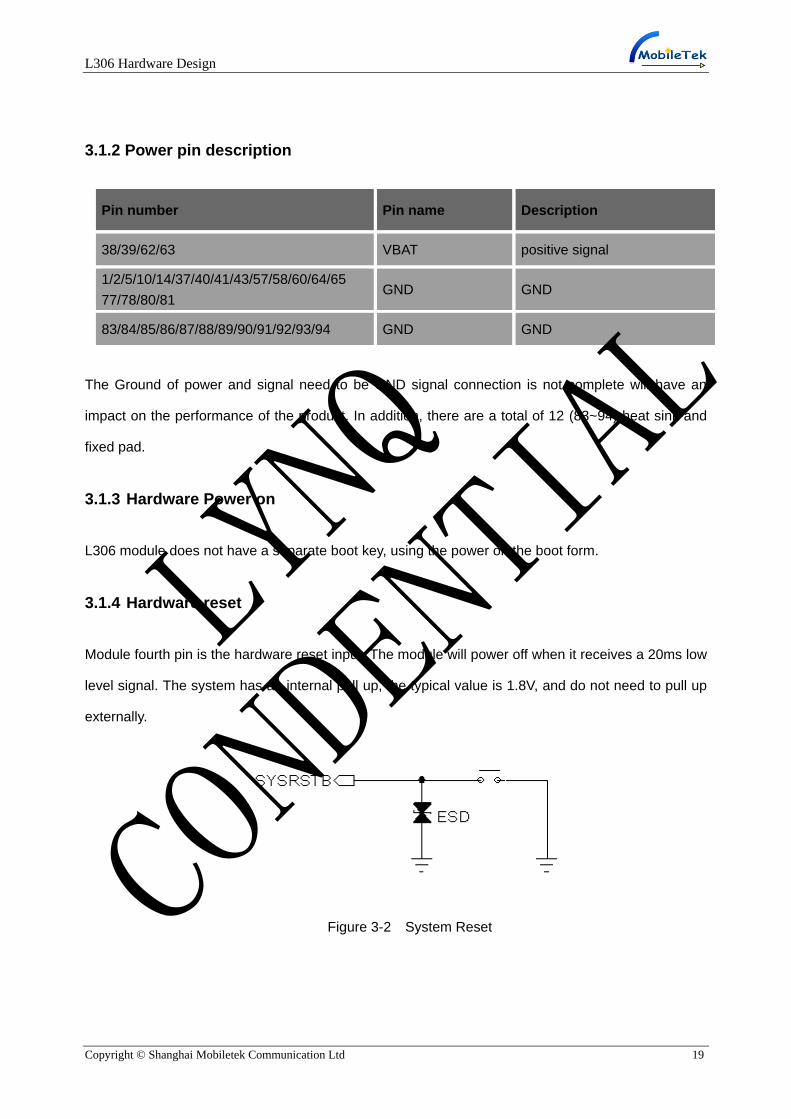
3.1.4 Hardware reset
Module fourth pin is the hardware reset input. The module will power off when it receives a 20ms low
level signal. The system has an internal pull up, the typical value is 1.8V, and do not need to pull up
externally.
Figure 3-2 System Reset
LYNQ
CONDENTIAL

L306 Hardware Design
Copyright © Shanghai Mobiletek Communication Ltd 20
3.2 USIM Interface
3.2.1 Pin Description
L306 supports and be able to automatically detect 3.0V and 1.8V USIM card. USIM card interface
signal as shown in table 3-1.
Table 3-1 (U)SIM Pin Description
Pin NO. Pin Name Signal definition Function Description
17 USIM_DATA USIM card data pin USIM card DATA signal, I/O signal
18 USIM_Reset USIM card reset pin USIM card reset signal, output by
the module
19 USIM_CLK USIM card clock pin USIM card clock signal, output by
the module
20 USIM_VCC USIM output voltage USIM card power supply, output
by the module
3.2.2 USIM application
USIM card signal group (PIN number: 17, 18, 19, 20), near the USIM card seat on the line. Please
note to increase the ESD protection device.
In order to meet the requirements of 3GPP TS 51.010-1 protocol and EMC certification, the proposed
USIM card is arranged near the position module USIM card interface, and avoid to layout too long
resulting in serious waveform distortion, affecting the signal integrity. USIM_CLK and USIM_DATA
signals are recommended to be protected. Between GND and USIM_VCC in parallel with a 1uF and
33pF capacitors, that can filter out the interference of radio frequency signals.
LYNQ
CONDENTIAL
L306 Hardware Design
Copyright © Shanghai Mobiletek Communication Ltd 21
Figure 3-3 (U)SIM Circuit
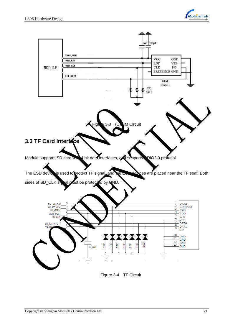
3.3 TF Card Interface
Module supports SD card with 4 bit data interfaces, and supports SDIO2.0 protocol.
The ESD device is used to protect TF signal, and the ESD devices are placed near the TF seat. Both
sides of SD_CLK signal must be protected by GND.
Figure 3-4 TF Circuit
LYNQ
CONDENTIAL
L306 Hardware Design
Copyright © Shanghai Mobiletek Communication Ltd 22
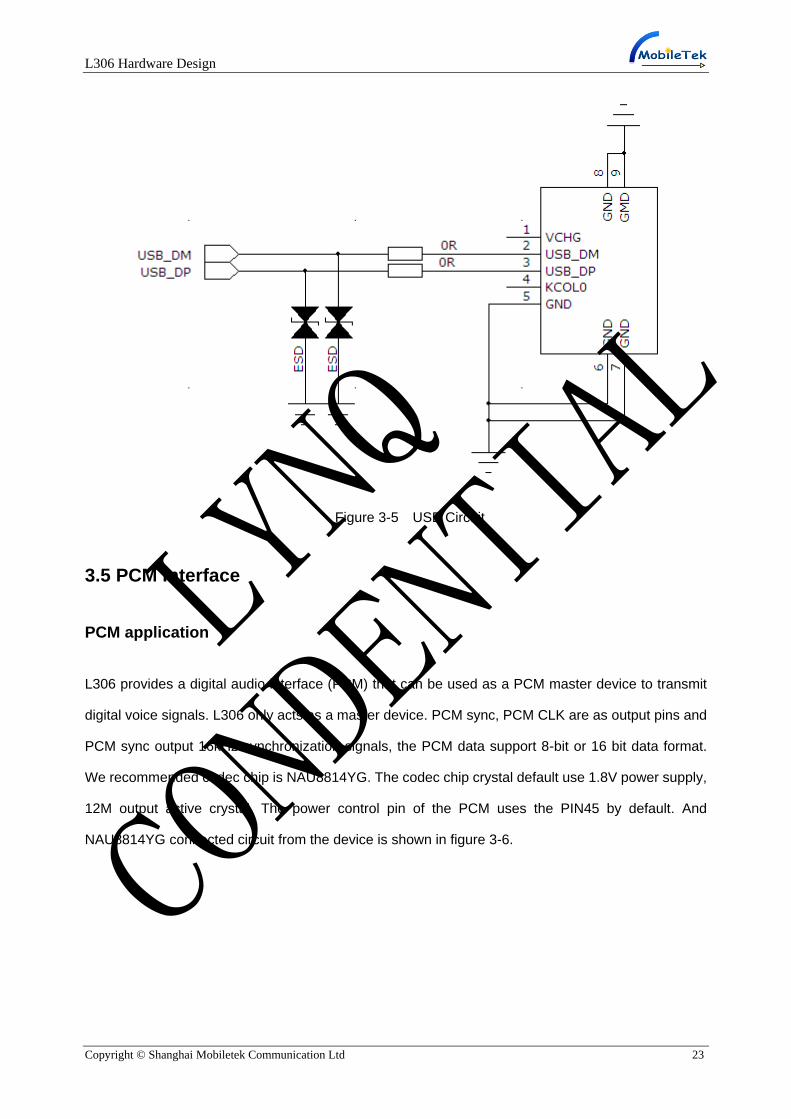
3.4 USB Interface
USB application
The USB interface of the module conforms to the USB2.0 specification and electrical characteristics.
Support the low-speed, full-speed and high-speed three operating modes. The data exchange
between the main processor (AP) and the module is mainly completed through the USB interface.
USB bus is mainly used for data transmission, software upgrade, module program testing. Working in
the USB mode of the high-speed line, if you need ESD design, ESD protection devices must meet the
junction capacitance value of <3pf, otherwise the larger junction capacitance will cause waveform
distortion, and affect the bus communication. The differential impedance of differential data lines
should be controlled at 90ohm ±10%, and lines should be protected up and down, and can’t be
crossed with other lines. USB connection circuit is as follows.
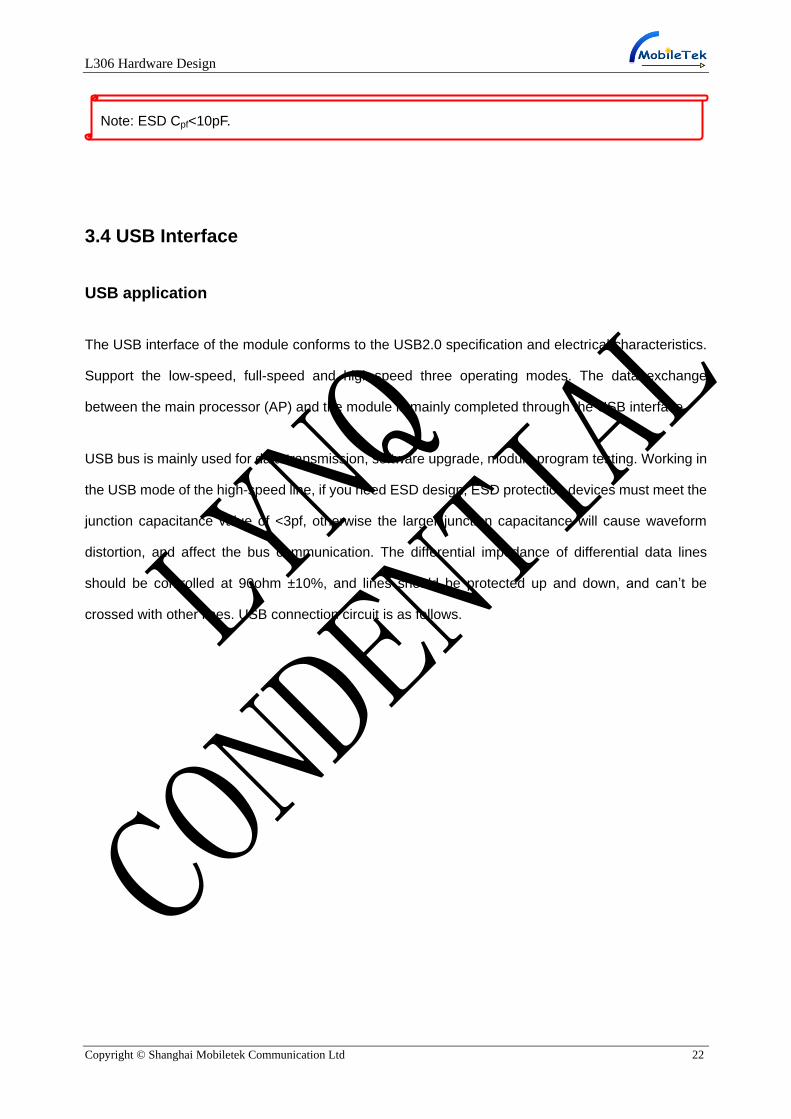
Note: ESD Cpf<10pF.
LYNQ
CONDENTIAL
L306 Hardware Design
Copyright © Shanghai Mobiletek Communication Ltd 23
Figure 3-5 USB Circuit
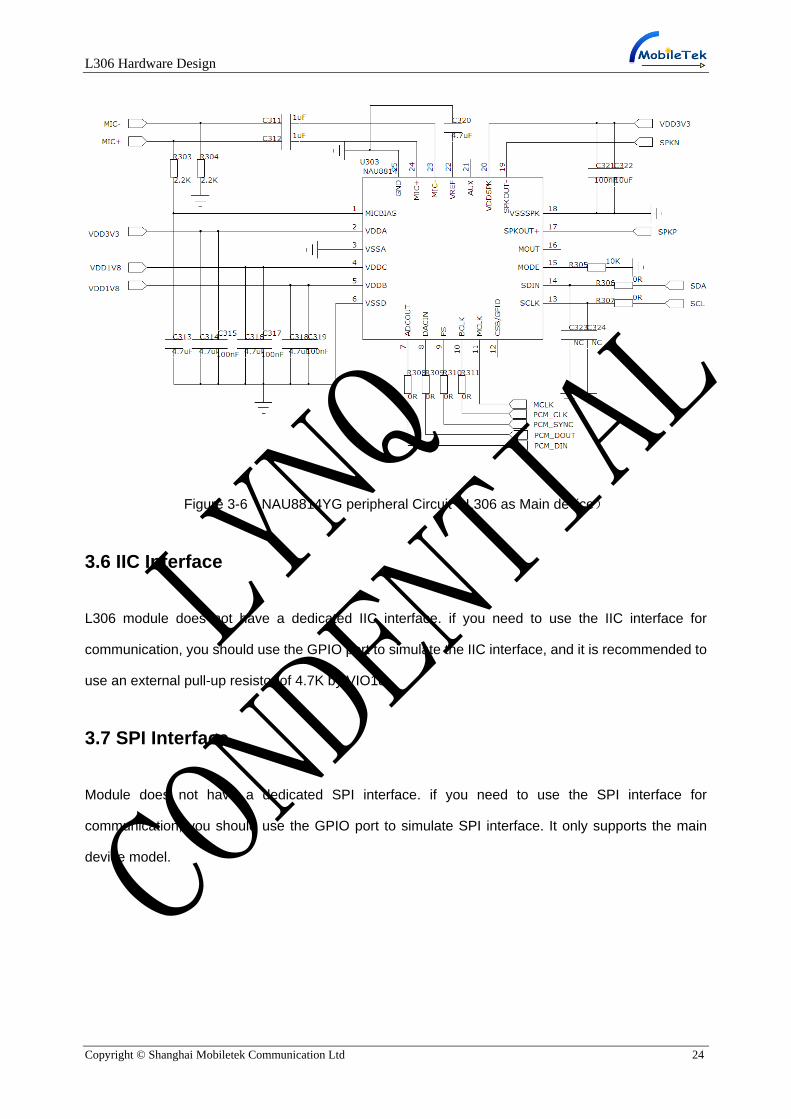
3.5 PCM Interface
PCM application
L306 provides a digital audio interface (PCM) that can be used as a PCM master device to transmit
digital voice signals. L306 only acts as a master device. PCM sync, PCM CLK are as output pins and
PCM sync output 16kHz synchronization signals, the PCM data support 8-bit or 16 bit data format.
We recommended codec chip is NAU8814YG. The codec chip crystal default use 1.8V power supply,
12M output active crystal. The power control pin of the PCM uses the PIN45 by default. And
NAU8814YG connected circuit from the device is shown in figure 3-6.
LYNQ
CONDENTIAL
L306 Hardware Design
Copyright © Shanghai Mobiletek Communication Ltd 24
Figure 3-6 NAU8814YG peripheral Circuit(L306 as Main device)
3.6 IIC Interface
L306 module does not have a dedicated IIC interface. if you need to use the IIC interface for
communication, you should use the GPIO port to simulate the IIC interface, and it is recommended to
use an external pull-up resistor of 4.7K by VIO18.
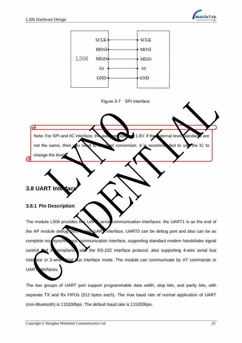
3.7 SPI Interface
Module does not have a dedicated SPI interface. if you need to use the SPI interface for
communication, you should use the GPIO port to simulate SPI interface. It only supports the main
device model.
LYNQ
CONDENTIAL
L306 Hardware Design
Copyright © Shanghai Mobiletek Communication Ltd 25
Figure 3-7 SPI Interface
3.8 UART Interface
3.8.1 Pin Description
The module L306 provides two UART serial communication interfaces: the UART1 is as the end of
the AP module debug port, 2-wire UART interface; UART0 can be debug port and also can be as
complete non-synchronous communication interface, supporting standard modem handshake signal
control and in compliance with the RS-232 interface protocol, also supporting 4-wire serial bus
interface or 2-wire serial bus interface mode. The module can communicate by AT commands or
UART interfaces.
The two groups of UART port support programmable data width, stop bits, and parity bits, with
separate TX and Rx FIFOs (512 bytes each). The max baud rate of normal application of UART
(non-Bluetooth) is 115200bps. The default baud rate is 115200bps.
Note: For SPI and IIC interface, the average power is 1.8V. if the external level standards are
not the same, then you need to do level conversion. It is recommended to use the IC to
change the level.
LYNQ
CONDENTIAL
L306 Hardware Design
Copyright © Shanghai Mobiletek Communication Ltd 26
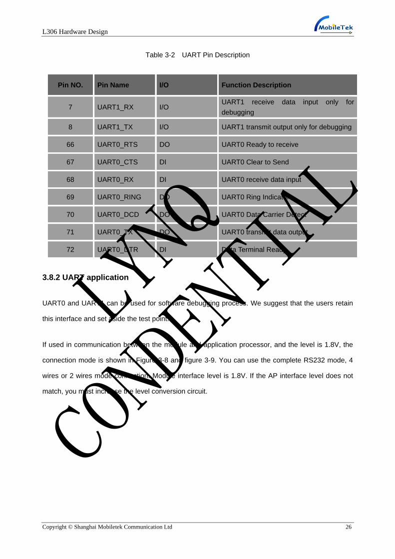
Table 3-2 UART Pin Description
Pin NO. Pin Name I/O Function Description
7 UART1_RX I/O UART1 receive data input only for
debugging
8 UART1_TX I/O UART1 transmit output only for debugging
66 UART0_RTS DO UART0 Ready to receive
67 UART0_CTS DI UART0 Clear to Send
68 UART0_RX DI UART0 receive data input
69 UART0_RING DO UART0 Ring Indicator
70 UART0_DCD DO UART0 Data Carrier Detect
71 UART0_TX DO UART0 transmit data output
72 UART0_DTR DI Data Terminal Ready
3.8.2 UART application
UART0 and UART1 can be used for software debugging process. We suggest that the users retain
this interface and set aside the test point.
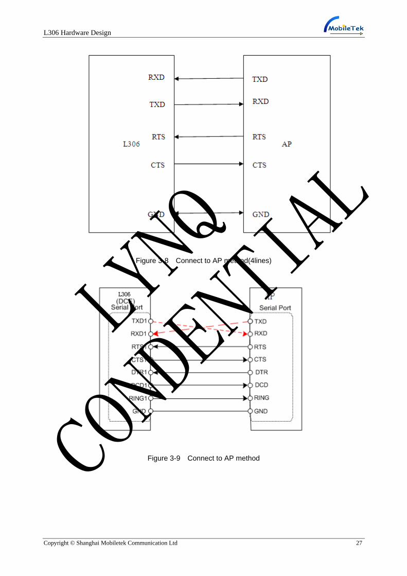
If used in communication between the module and application processor, and the level is 1.8V, the
connection mode is shown in Figure 3-8 and figure 3-9. You can use the complete RS232 mode, 4
wires or 2 wires mode connection. Module interface level is 1.8V. If the AP interface level does not
match, you must increase the level conversion circuit. LYNQ
CONDENTIAL
L306 Hardware Design
Copyright © Shanghai Mobiletek Communication Ltd 27
Figure 3-8 Connect to AP method(4lines)
Figure 3-9 Connect to AP method
LYNQ
CONDENTIAL
L306 Hardware Design
Copyright © Shanghai Mobiletek Communication Ltd 28
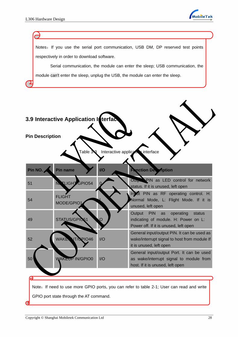
3.9 Interactive Application Interface
Pin Description
Table 3-3 Interactive application interface
Pin NO. Pin name I/O Function Description
51 NETLIGHT/GPIO54 0 Output PIN as LED control for network
status. If it is unused, left open
54 FLIGHT
MODE/GPIO1 I
Input PIN as RF operating control. H:
Normal Mode, L: Flight Mode. If it is
unused, left open
49 STATUS/GPIO51 O
Output PIN as operating status
indicating of module. H: Power on L:
Power off. If it is unused, left open
52 WAKEOUT/GPIO46 I/O
General input/output PIN. It can be used as
wake/interrupt signal to host from module If
it is unused, left open
50 WAKEUP IN/GPIO0 I/O
General input/output Port. It can be used
as wake/interrupt signal to module from
host. If it is unused, left open
Note:If need to use more GPIO ports, you can refer to table 2-1; User can read and write
GPIO port state through the AT command.
Notes:If you use the serial port communication, USB DM, DP reserved test points
respectively in order to download software.
Serial communication, the module can enter the sleep; USB communication, the
module can't enter the sleep, unplug the USB, the module can enter the sleep.
LYNQ
CONDENTIAL
L306 Hardware Design
Copyright © Shanghai Mobiletek Communication Ltd 29
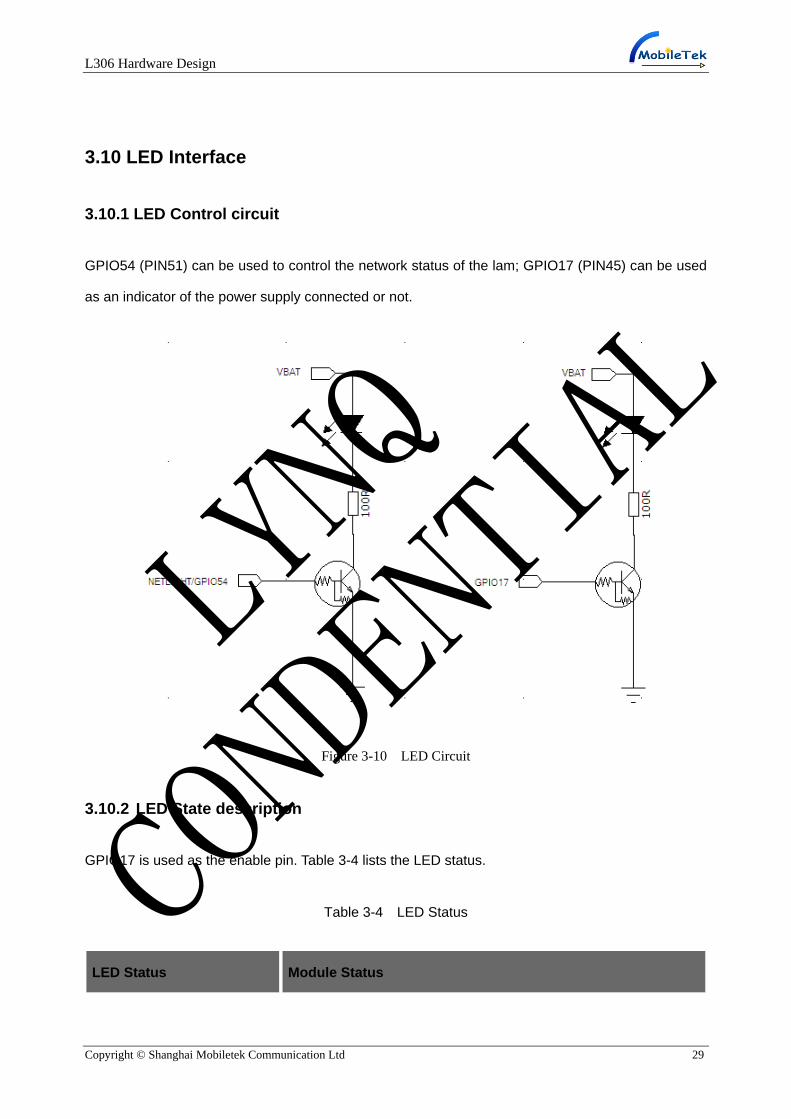
3.10 LED Interface
3.10.1 LED Control circuit
GPIO54 (PIN51) can be used to control the network status of the lam; GPIO17 (PIN45) can be used
as an indicator of the power supply connected or not.
Figure 3-10 LED Circuit
3.10.2 LED State description
GPIO17 is used as the enable pin. Table 3-4 lists the LED status.
Table 3-4 LED Status
LED Status Module Status
LYNQ
CONDENTIAL

L306 Hardware Design
Copyright © Shanghai Mobiletek Communication Ltd 30
Always On Power on
OFF Power off
GPIO54 is used as the enable pin. Table 3-5 lists the LED status.
Table 3-5 LED Status
LED Status Module Status
Always On Searching Network/Call Connect
200ms ON, 200ms OFF Data Transmit
800ms ON, 800ms OFF Registered network
OFF Power off / Sleep
LYNQ
CONDENTIAL
L306 Hardware Design
Copyright © Shanghai Mobiletek Communication Ltd 31
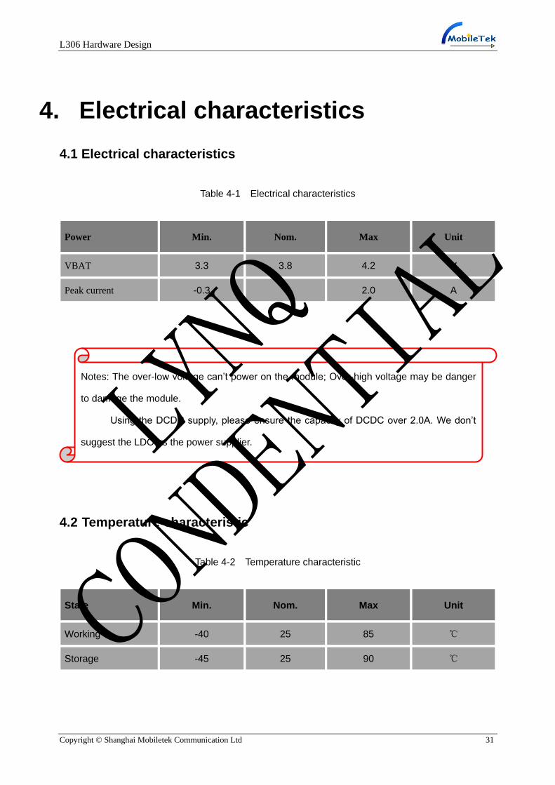
4. Electrical characteristics
4.1 Electrical characteristics
Table 4-1 Electrical characteristics
Power Min. Nom. Max Unit
VBAT 3.3 3.8 4.2 V
Peak current -0.3 - 2.0 A
4.2 Temperature characteristic
Table 4-2 Temperature characteristic
State Min. Nom. Max Unit
Working -40 25 85 ℃
Storage -45 25 90 ℃
Notes: The over-low voltage can’t power on the module; Over-high voltage may be danger
to damage the module.
Using the DCDC supply, please ensure the capacity of DCDC over 2.0A. We don’t
suggest the LDO as the power supplier.
LYNQ
CONDENTIAL
L306 Hardware Design
Copyright © Shanghai Mobiletek Communication Ltd 32
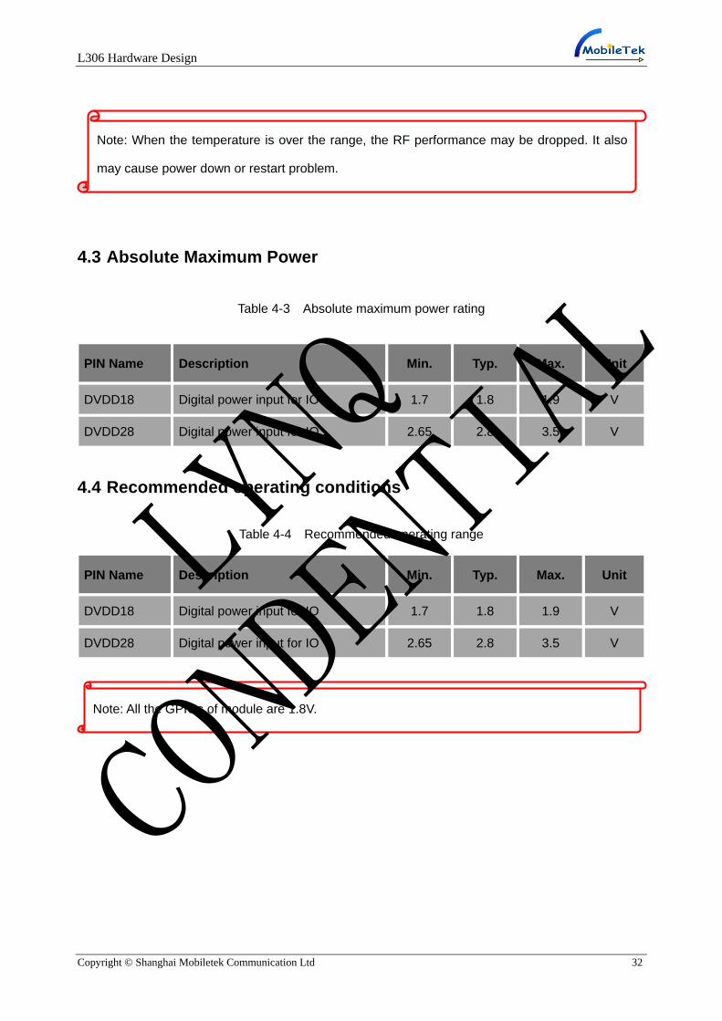
4.3 Absolute Maximum Power
Table 4-3 Absolute maximum power rating
PIN Name Description Min. Typ. Max. Unit
DVDD18 Digital power input for IO 1.7 1.8 1.9 V
DVDD28 Digital power input for IO 2.65 2.8 3.5 V
4.4 Recommended operating conditions
Table 4-4 Recommended operating range
PIN Name Description Min. Typ. Max. Unit
DVDD18 Digital power input for IO 1.7 1.8 1.9 V
DVDD28 Digital power input for IO 2.65 2.8 3.5 V
Note: All the GPIOs of module are 1.8V.
Note: When the temperature is over the range, the RF performance may be dropped. It also
may cause power down or restart problem.
LYNQ
CONDENTIAL
L306 Hardware Design
Copyright © Shanghai Mobiletek Communication Ltd 33
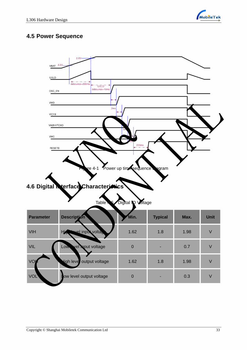
4.5 Power Sequence
Figure 4-1 Power up time sequence diagram
4.6 Digital Interface Characteristics
Table 4-5 Digital IO Voltage
Parameter Description Min. Typical Max. Unit
VIH High level input voltage 1.62 1.8 1.98 V
VIL Low level input voltage 0 - 0.7 V
VOH High level output voltage 1.62 1.8 1.98 V
VOL Low level output voltage 0 - 0.3 V
LYNQ
CONDENTIAL
L306 Hardware Design
Copyright © Shanghai Mobiletek Communication Ltd 34
4.7 ESD
Because there is no special protection against electrostatic discharge in the module, it is necessary to
pay attention to the protection of electrostatic protection in the production, assembly and operation
module. The performance parameters of the module test are as follows.
ESD parameter(Tem:25℃,humidity:45%).
Table 4-7 ESD Performance
PIN Name Contact discharge Air discharge
VBAT ±4KV ±8KV
GND ±4KV ±8KV
RF_ANT ±4KV ±8KV
Enhanced ESD performance method:
1、 If the customer to the adapter plate, the adapter plate anchor as much as possible, and the
uniform distribution of conduction path width;
2、 The suspension plate (key board or light board, etc.) need to be well grounded, for grounding
copper exposure;
3、 Key (reset key) need to add ESD device; reset key to walk the line do not rely on the edge of the
board;
4、 USB, UART and other plug connection need to add ESD devices, the other from the outside of
Note: Suit to all GPIO, IIC, UART, SPI interfaces.
LYNQ
CONDENTIAL
L306 Hardware Design
Copyright © Shanghai Mobiletek Communication Ltd 35
the machine out of the control line also need to add ESD devices;
5、 SIM card, users will get inserted t-card touch the place also need to add ESD device;
6、 External antenna, please add ESD device, ESD Cpf<0.5pF.
Notes: For ESD protect, please add ESD methods according to upper ways.
High speed circuits like USB, TF and SIM card should be added ESD with low
capacity value.
ESD components include varistors and TVS. For better performance, please use
TVS.
LYNQ
CONDENTIAL
L306 Hardware Design
Copyright © Shanghai Mobiletek Communication Ltd 36
5. RF Features
5.1 Frequency Band
L306 supports GSM Band 2/3/5/8 and WCDMA Band1(2)/Band8(5).
Table 5-1 Frequency Bands
Frequency Uplink Downlink
GSM850 824 MHz — 849 MHz 869 MHz — 894 MHz
E-GSM900 880 MHz — 915 MHz 925 MHz — 960 MHz
DCS1800 1710 MHz — 1785 MHz 1805 MHz — 1880 MHz
PCS1900 1850 MHz — 1910 MHz 1930 MHz — 1990 MHz
UMTS2100 1920 MHz — 1980 MHz 2110 MHz — 2170 MHz
UMTS1900 1850 MHz — 1910 MHz 1930 MHz — 1990 MHz
UMTS850 824 MHz — 849MHz 869 MHz — 894 MHz
UMTS900 880 MHz — 915 MHz 925 MHz — 960 MHz
Table 5-2 Output power
Frequency Max output power Min output power
GSM850 33dBm ±2dB 5dBm ±5dB
E-GSM900 33dBm ±2dB 5dBm ±5dB
DCS1800 30dBm ±2dB 0dBm ±5dB
PCS1900 30dBm ±2dB 0dBm ±5dB
GSM850(8-PSK) 27dBm ±3dB 5dBm ±5dB
E-GSM900(8-PSK) 27dBm ±3dB 5dBm ±5dB
LYNQ
CONDENTIAL
L306 Hardware Design
Copyright © Shanghai Mobiletek Communication Ltd 37
DCS1800(8-PSK) 26dBm +3/-4dB 0dBm ±5dB
PCS1900(8-PSK) 26dBm +3/-4dB 0dBm ±5dB
UMTS2100 24dBm +1/-3dB -56dBm ±5dB
UMTS1900 24dBm +1/-3dB -56dBm ±5dB
UMTS850 24dBm +1/-3dB -56dBm ±5dB
UMTS900 24dBm +1/-3dB -56dBm ±5dB
Table 5-3 Receive sensitivity
Frequency Receive sensitivity
GSM850 <-109dBm
E-GSM900 <-109dBm
DCS1800 <-109dBm
PCS1900 <-109dBm
UMTS2100 <-109dBm
UMTS1900 <-109dBm
UMTS850 <-109dBm
UMTS900 <-109dBm
5.2 Data link
L306 supports GPRS/EDGE CLASS12,and HSDPA/HSDPA R8. The actual application depends on
the local network operator.
Table 5-4 Data Link
Version Function Max supported Theoretical max peak rate
L306 GPRS CS4 85.6kbps
LYNQ
CONDENTIAL
L306 Hardware Design
Copyright © Shanghai Mobiletek Communication Ltd 38
L306 EDGE MCS9 236.8kbps
L306E/A HSDPA Cat10 14.4Mbps
L306ME/MA HSDPA Cat14 21Mbps
L306HE/HA HSDPA Cat24 42Mbps
L306E/A HSUPA Cat6 5.76Mbps
L306ME/MA HSUPA Cat7 11Mbps
L306HE/HA HSUPA Cat7 11Mbps
5.3 Antenna Design
The access part of the RF antenna of this product supports the PAD form. The connection between
the module and the main board antenna interface is required to be welded and connected through a
microstrip line or a strip line. The microstrip line or strip line is designed according to the characteristic
impedance of 50 ohm, and the length of the wire is less than 10mm. Reserved ∏ matching network
Antenna efficiency
Antenna efficiency is the ratio of the input power and radiant power. Because of the return loss,
material loss and coupling loss of the antenna, the radiant power is always lower than the input power.
The ratio is recommended to be controlled over 40%(-4dB).
S11 or VSWR
S11 indicates the matching level of the 50 Ohm impedance for the antenna. It affects the antenna
efficiency in a certain extent. The VSWR testing method could be used for measuring purpose. The
recommended value for S11 is less than -10dB.
Polarization
Polarization refers to the rotation direction of electric field while the antenna is in the direction of
maximum radiation. Linear polarization is recommended. It is recommended to use the diversity
antenna which has the different polarization direction from the main antenna.
LYNQ
CONDENTIAL
L306 Hardware Design
Copyright © Shanghai Mobiletek Communication Ltd 39
Radiation pattern
The radiation pattern refers to the intensity of the electromagnetic field while the antenna is in every
direction of the far field. Dipole antenna is perfect as the terminal antenna. For built-in antenna, it is
recommended to use PIFA or IFA antennas.
Antenna dimension: 6mm*10mm*100mm (H*W*L).
Antenna radiation direction: omnidirectional.
Gain and directivity
Antenna directivity refers to the intensity of the electromagnetic field while the electromagnetic wave
is in all directions. Gain is the collection of the efficiency and directivity of the antenna. It is
recommended that antenna gain is less than or equal to 3dBi.
Interference
In addition to antenna performance, some other interference from the PCB will also affect the module
performance. To ensure the high performance of the module, the interference must be under control.
Suggestions: keep speaker, LCD, CPU, FPC wire routing, audio circuits, and power supply away from
the antenna, and add appropriate filtering and shielding protection, or adding filtering devices on the
traces.
TRP/TIS
TRP(Total Radiated Power):
GSM850/900 >28dBm
GSM1800/1900 >25dBm
WCDMA Band1/8 >19dBm
TIS(Total Isotropic Sensitivity):
GSM850/900/1800/1900 <-102dBm
WCDMA Band1/8 <-102dBm
LYNQ
CONDENTIAL
L306 Hardware Design
Copyright © Shanghai Mobiletek Communication Ltd 40
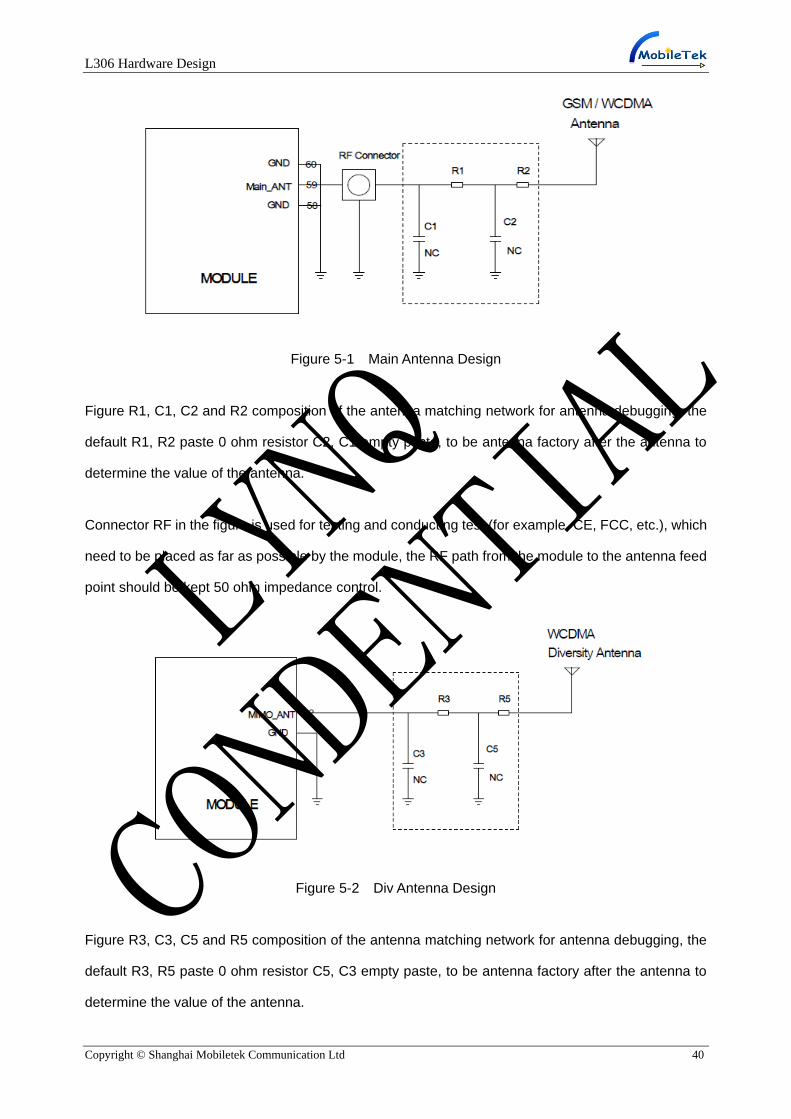
Figure 5-1 Main Antenna Design
Figure R1, C1, C2 and R2 composition of the antenna matching network for antenna debugging, the
default R1, R2 paste 0 ohm resistor C2, C1 empty paste, to be antenna factory after the antenna to
determine the value of the antenna.
Connector RF in the figure is used for testing and conducting test (for example, CE, FCC, etc.), which
need to be placed as far as possible by the module, the RF path from the module to the antenna feed
point should be kept 50 ohm impedance control.
Figure 5-2 Div Antenna Design
Figure R3, C3, C5 and R5 composition of the antenna matching network for antenna debugging, the
default R3, R5 paste 0 ohm resistor C5, C3 empty paste, to be antenna factory after the antenna to
determine the value of the antenna.
LYNQ
CONDENTIAL
L306 Hardware Design
Copyright © Shanghai Mobiletek Communication Ltd 41
6. Storage and Production
6.1 Storage
The rank of moisture proof of the module is level 3. There is an obvious sign on the table of the
internal and the external packaging.
In the vacuum sealed bag, the module can be stored for 120 days when the temperature is 18~28℃
and the humidity is 40~65%.
6.2 Production
The module is a humidity sensitive device. If the device needs reflow soldering, disassembly and
maintenance, we must strictly comply with the requirements of humidity sensitive device. If module is
damp, a reflow soldering or using a hot-air gun maintenance will lead to internal damage, because
the water vapor has the rapid expansion of the burst, causing physical injury to the device, like PCB
foaming and BGA component fail. So customers should refer to the following recommendations.
6.2.1 Module confirmation and moisture
The module in the production and packaging process should be strictly accordance with the humidity
sensitive device operation. The factory packaging is vacuum bag, desiccant, and humidity indicator
card. Please pay attention to the moisture control before SMT and the confirmation of the following
aspects.
Product packaging confirmation
In order to ensure quality, smart module uses vacuum packaging and shipment, to avoid the question
of SMT and function for the moisture in the air. Therefore, the requirements to confirm for the
packaging of products before the SMT are necessary, ensuring the packaging not damaged, vacuum
LYNQ
CONDENTIAL
L306 Hardware Design
Copyright © Shanghai Mobiletek Communication Ltd 42
packing not leaks. If there is any breakage and leakage, the Module should be baked, to avoid PCB
foaming, BGA chip and RF PA chip fail.
Production cycle confirmation
The customer needs to confirm the production cycle of the product when receiving the product. If it
exceed the storage period or the product has been affected with damp, the product must be baked. If
the storage time not extended, and after opening the packaging, humidity indicator card is at 10%
without discoloration, it indicate good packaging and can be normally used.
Humidity indicator card confirmation
If the module has according to the moisture level 3 processing, and internal packaging have been
placed humidity indicator cards, customers should confirm the humidity indicator card before SMT. If
the humidity indicator card has changed more than 10%, it need to carry on the material baking.
Baking condition confirmation
The moisture proof level of the smart module is level 3. And the baking conditions are as follows.
Table 6-1 Baking conditions
Baking conditions
90°/ 5%RH 60°/ 5%RH(Recommended)
40°/ 5%RH
Baking time 48 hours 72 hours 30days
Description not use the original tray not use the original tray Can use the original tray
Customers can also choose baking conditions according to their own conditions. But please refer to
Level 3 and device thickness 1.4 ~ 2.0mm standard.
L306 Hardware Design
Copyright © Shanghai Mobiletek Communication Ltd 43
Factory life confirmation
Module SMT with good humidity control should be completed in 48 hours after opening the package.
The unused Module should be vacuum packaging, and placed in a drying box. If exposure to air for
more than 48 hours, the module need to be baked. Due to the larger size of the module, damp needs
to bake for a long time, and the price is high, so please try to run out after opening the package.
Customer product maintenance
If maintenance module after SMT, it is easy for damp module to damage when removing, so the
module disassembly and other related maintenance operations should complete within 48 hours after
SMT, or need to bake and then maintenance the module.
Because the module return from the field work can’t ensure the dry state, it must be baked in
accordance with the conditions of baking, then for disassembly and maintenance. If it has been
exposed to the humid environment for a long time, please properly extend the baking time, such as
125 degrees /36 hours.
6.2.2 SMT reflow attentions
The module has the BGA chips, chip resistances and capacitances internally, which will melt at high
temperature. If module melt completely encountered a large shock, such as excessive vibration of
reflux conveyor belt or hit the board, internal components will easily shift or be false welding. So,
using intelligent modules over the furnace need to pay attention to:
Notes: The original anti-ESD tray temperature does not exceed 50 degree. Otherwise the
tray will be deformed.
The anti-ESD tray of the original packaging is only used for packaging, and can’t be
used as a SMT tray.
L306 Hardware Design
Copyright © Shanghai Mobiletek Communication Ltd 44
Modules can’t be vibrate larger, namely customer requirements as far as possible in orbit (chain)
furnace, furnace, avoid on the barbed wire furnace, in order to ensure smooth furnace.
The highest temperature can’t too high. In the condition that meet the welding quality of
customer motherboard and module, the lower furnace temperature and the shorter maximum
temperature time, the better.
Some customer’s temperature curve in the line is not suitable, high temperature is too high, and
customer motherboard melt good, but non-performing rate is on the high side. Through the analysis
of the causes, it found that melt again of BGA components lead device offset and short circuit. After
adjusting the temperature curve, it can ensure that the customer’s motherboard the welding quality,
and also improve the pass through rate. Non-performing rate is controlled below the 2/10000.
6.2.3 SMT stencil design and the problem of less tin soldering
Part of customers found false welding or circuit short when reflowing. The main reason is module tin
less, PCB distortion or tins too large. Suggestions are as follows:
Suggest use ladder stencil 0.10-0.18mm, which means the region of module is proposed to
0.18mm stencil thickness. Please adjust validation according to the measured thickness of
solder paste, the actual company conditions and experience value. The products need to strictly
test.
Stencil: Reference module package, and the user can adjust according to their company
experience. Outside of the module, the stencil extends to 0.3mm outside. The GND pads use the
net stencil.
In the production process, if you cannot judge the opening or process conditions, you can also
contact our sales or after-sales service. We will give specific recommendations according to the
actual situation.
L306 Hardware Design
Copyright © Shanghai Mobiletek Communication Ltd 45
6.2.4 SMT attentions
If customer motherboard is thin and slender with a furnace deformation, warping risks, you will be
suggested to create "a furnace vehicle" to ensure the welding quality. Other production proposals are
as follows:
The solder pastes use brands like Alfa;
The module must use the SMT machine mount (important), and do not recommend manually
placed or manual welding.
Please strictly control the pressure and speed in SMT (very important);
We must use the reflow oven more than 8 temperature zones, and strictly control the furnace
temperature curve.
Recommended temperature:
B. constant temperature zone: temperature 160-190°C, time: 60s-100s.
E. recirculation zone: PEAK temperature 235-245°C, time over 220°C: 30s-60s.
Notes: Customer’s board deformation must be controlled within 0.15mm. By reducing the
number of imposition or increasing patch clamp to reduce the deformation.
Module thickness of the stencil is recommended to be thickened to 0.18mm, and the
rest position can be maintained by 0.1mm.
Related Documents


![QUÍMICOS DEL SUR BOLETÍN SEMANAL INFORMATIVO ......Newssheet Up Internacional. Nº 95. 28 de noviembre de 2017. BOLETINES OFICIALES DOUE L306 de 22.11.2017 [19] Decisión de Ejecución](https://static.cupdf.com/doc/110x72/5feee0ffd395d76d1a05a77f/qumicos-del-sur-boletn-semanal-informativo-newssheet-up-internacional.jpg)

