〇Product structure : Silicon monolithic integrated circuit 〇This product has no designed protection against radioactive rays 1/28 © 2017 ROHM Co., Ltd. All rights reserved. www.rohm.com TSZ22111・14・001 TSZ02201-0252AAJ00080-1-2 2017.05.10 Rev.001 4.5V to 42V Input Voltage Range 1.5A Output Current Integrated FET 1ch Buck Converter BD9G201EFJ-M General Description BD9G201EFJ is a buck converter with built-in high side MOSFET. It has an input voltage range of 4.5V to 42V. Current mode architecture provides fast transient response and a simple phase compensation setup. The IC is mainly used as a secondary side power supply: for example, a step-down output of 3.3V/5V can be produced from voltage power supply such as 12V or 24V. In addition, it has a synchronization function with an external CLK that provides noise management. Features AEC-Q100 Qualified (Note 1) Integrated Nch MOSFET Synchronizes to external clock 250kHz to 500kHz ON/OFF Control through EN Terminal (Standby current of 0μA) Small package(HTSOP-J8ES) LowDrop Out operation (Note1: Grade 2) Applications Automotive applications (Navigation system, Audio system, etc.) Industrial distributed-power applications Entertainment equipment Consumer devices in general that has 12V/24V lines Key Specifications Input Voltage range: 4.5V to 42V Reference voltage precision (Ta= 25°C) ±1.5% (Ta= -40 to +105°C) ±2.0% Max Output Current: 1.5A(Max) Operating Temperature range: -40°C to +105°C Package W (Typ) x D (Typ) x H (Max) HTSOP-J8ES 4.90mm x 6.00mm x 1.00mm Typical Application Circuit VCC VOUT 0.01μF EN LX GND VC FB VCC BST EN SYNC SYNC CVCC : 10μF/50V COUT : 47μF/16V 0.1μF 160kΩ 5V/1.5A R4 R5 30kΩ 4.7kΩ D1 L1: 22μH HTSOP-J8ES Figure 1. Typical Application Circuit Datasheet

Welcome message from author
This document is posted to help you gain knowledge. Please leave a comment to let me know what you think about it! Share it to your friends and learn new things together.
Transcript
〇Product structure : Silicon monolithic integrated circuit 〇This product has no designed protection against radioactive rays
1/28 © 2017 ROHM Co., Ltd. All rights reserved. www.rohm.com
TSZ22111・14・001
TSZ02201-0252AAJ00080-1-2
2017.05.10 Rev.001
4.5V to 42V Input Voltage Range 1.5A Output Current Integrated FET
1ch Buck Converter BD9G201EFJ-M
General Description BD9G201EFJ is a buck converter with built-in high side MOSFET. It has an input voltage range of 4.5V to 42V. Current mode architecture provides fast transient response and a simple phase compensation setup. The IC is mainly used as a secondary side power supply: for example, a step-down output of 3.3V/5V can be produced from voltage power supply such as 12V or 24V. In addition, it has a synchronization function with an external CLK that provides noise management.
Features AEC-Q100 Qualified
(Note 1)
Integrated Nch MOSFET Synchronizes to external clock 250kHz to 500kHz ON/OFF Control through EN Terminal
(Standby current of 0µA) Small package(HTSOP-J8ES) LowDrop Out operation (Note1: Grade 2)
Applications Automotive applications
(Navigation system, Audio system, etc.) Industrial distributed-power applications Entertainment equipment Consumer devices in general that has 12V/24V lines
Key Specifications Input Voltage range: 4.5V to 42V
Reference voltage precision (Ta= 25°C) ±1.5% (Ta= -40 to +105°C) ±2.0%
Max Output Current: 1.5A(Max)
Operating Temperature range: -40°C to +105°C
Package W (Typ) x D (Typ) x H (Max) HTSOP-J8ES 4.90mm x 6.00mm x 1.00mm
Typical Application Circuit
VCCVOUT
0.01μF
EN
LX
GND
VC
FB
VCC
BST
EN
SYNC SYNC
CVCC
: 10µF/50V
COUT
: 47µF/16V
0.1µF
160kΩ
5V/1.5A
R4
R5
30kΩ 4.7kΩ
D1
L1: 22µH
HTSOP-J8ES
Figure 1. Typical Application Circuit
Datasheet

2/28
BD9G201EFJ-M
© 2017 ROHM Co., Ltd. All rights reserved. www.rohm.com
TSZ22111・15・001
TSZ02201-0252AAJ00080-1-2 2017.05.10 Rev.001
EN
0.8V
ErrorAMP
VCC
LX
REFUVLO
140mΩ
SoftStart
ON/OFF
GND
+
-+
FB
BST
TSD
shutdown
10Ω
VC
R Q
Current Sense AMP
VOUT
SYNC
Oscillator
+
-
REG
S
MaxdutyLogic
10μA
+-1.8V
Nch FET SW
ENUVLO
CHG
OCP
Σ
Current Sense
Pin Configuration
LX 1
GND 2
VC 3 6 EN
8 VCC
FB 4 5 SYNC
7 BSTTHERMAL
PAD
(TOP_VIEW)
Pin Description
Pin No. Pin Name Description
1 LX Switching terminal
2 GND Ground terminal
3 VC Error amplifier output terminal
4 FB Feedback input terminal
5 SYNC External clock input terminal
6 EN Enable terminal
7 BST Terminal for boot-strap capacitor
8 VCC Power supply terminal
- THERMAL PAD PAD for heat dissipation. Always connect to GND.
Block Diagram
Figure 2. Pin Configuration
Figure 3. Block Diagram

3/28
BD9G201EFJ-M
© 2017 ROHM Co., Ltd. All rights reserved. www.rohm.com
TSZ22111・15・001
TSZ02201-0252AAJ00080-1-2 2017.05.10 Rev.001
Description of Blocks
1. REF This block generates the reference voltage.
2. REG
Regulator for internal circuit power supply.
3. CHG Regulator for bootstrap capacitor charging.
4. TSD Thermal Shutdown Protection Circuit When it detects the temperature exceeding Maximum Junction Temperature (Tj= 150°C), it turns off the output FET, and resets SoftStart circuit. It has a hysteresis function. When the temperature is decreased, the chip automatically returns to normal operation.
5. UVLO Under Voltage Lock-Out Circuit This prevents internal circuit error during increase and decrease of power supply voltage. It monitors VCC terminal voltage. When VCC voltage becomes UVLO and below, it turns OFF output FET. SoftStart circuit also resets during this time. This circuit has a hysteresis.
6. ENUVLO If the voltage from this terminal is below 0.3V, IC operation is OFF. If it is between 0.3V and 1.4V, internal REG circuit turns ON. If it is greater than 1.8V(Typ), the IC is operational and a hysteresis generation current of 10 μA (Typ) is sourced from the internal circuit. To turn off the IC, source current should be removed. When the situation without a signal to control EN terminal at the time of startup is assumed, pull down EN terminal by pull down resistor to prevent becoming the high impedance. Arbitrary UVLO is possible by connecting EN terminal to a voltage divider from the input voltage.
7. ErrorAMP
This is an error amplifier circuit that detects the output signal, and outputs PWM control signal. Internal reference voltage is set to 0.8V(Typ).
8. SoftStart This is a circuit that gently raises the output voltage of the DC / DC converter to prevent in-rush current during start-up. SoftStart Time is 8ms (Typ) when the IC operates with the 300 kHz (Typ) internal clock. When the IC operates with an external clock, SoftStart Time is changed according to the oscillator frequency.
9. Oscillator This is a oscillation circuit with an operating frequency fixed to 300 kHz(Typ). By inputting external CLK to the SYNC terminal, synchronous operation of 250 kHz to 500 kHz can be achieved. When used in self-running mode, please connect SYNC terminal to GND.
10. Current Sense AMP This is a voltage - pulse width converter. It compares the voltage depending on the current of FET SW through the sum of the error amplifier output voltage and the slope ripple. The output then controls the width of the output pulse and outputs it to the driver.
11. Nch FET SW It should be used within OCP threshold 2.0A(Min) including the output current and ripple current of the inductor.
12. OCP The IC has a over current protection to protect the Nch FET from over current. When OCP is detected twice sequentially, the device will stop certain period of time and restart automatically.
13. MaxDuty logic When Nch FET SW continues being turned ON in continuous 8 cycles, the high side FET will be turned off forcibly.

4/28
BD9G201EFJ-M
© 2017 ROHM Co., Ltd. All rights reserved. www.rohm.com
TSZ22111・15・001
TSZ02201-0252AAJ00080-1-2 2017.05.10 Rev.001
Absolute Maximum Ratings (Ta= 25°C)
Parameter Symbol Limit Rating Unit
VCC-GND VCC 45 V
BST-GND VBST 50 V
BST-LX VBST-LX 7 V
EN-GND VEN 45 V
LX-GND VLX 45 V
FB-GND VFB 7 V
VC-GND VVC 7 V
SYNC-GND VSYNC 7 V
Operating Temperature range Topr -40 to +105 °C
Storage Temperature range Tstg -55 to +150 °C
Maximum Junction Temperature Tjmax 150 °C
Caution: Operating the IC over the absolute maximum ratings may damage the IC. The damage can either be a short circuit between pins or an open circuit between pins and the internal circuitry. Therefore, it is important to consider circuit protection measures, such as adding a fuse, in case the IC is operated over the absolute maximum ratings
Thermal Resistance(Note 1)
Parameter Symbol Thermal Resistance (Typ)
Unit 1s
(Note 3) 2s2p
(Note 4)
HTSOP-J8ES
Junction to Ambient θJA 206.4 45.2 °C/W
Junction to Top Characterization Parameter(Note 2)
ΨJT 21 13 °C/W
(Note 1)Based on JESD51-2A(Still-Air)
(Note 2)The thermal characterization parameter to report the difference between junction temperature and the temperature at the top center of the outside
surface of the component package.
(Note 3)Using a PCB board based on JESD51-3.
Layer Number of Measurement Board
Material Board Size
Single FR-4 114.3mm x 76.2mm x 1.57mmt
Top
Copper Pattern Thickness
Footprints and Traces 70μm
(Note 4)Using a PCB board based on JESD51-7.
Layer Number of Measurement Board
Material Board Size Thermal Via(Note 5)
Pitch Diameter
4 Layers FR-4 114.3mm x 76.2mm x 1.6mmt 1.20mm Φ0.30mm
Top 2 Internal Layers Bottom
Copper Pattern Thickness Copper Pattern Thickness Copper Pattern Thickness
Footprints and Traces 70μm 74.2mm x 74.2mm 35μm 74.2mm x 74.2mm 70μm
(Note 5) This thermal via connects with the copper pattern of all layers..

5/28
BD9G201EFJ-M
© 2017 ROHM Co., Ltd. All rights reserved. www.rohm.com
TSZ22111・15・001
TSZ02201-0252AAJ00080-1-2 2017.05.10 Rev.001
Recommended Operating Ratings (Ta= -40°C to +105°C)
Parameter Symbol Rating
Unit Min Typ Max
Power Supply Voltage VCC 4.5(Note 6)
- 42 V
Output Voltage VOUT 0.8 (Note 7)
- VCC (Note 8)
V
Output Current IOUT - - 1.5 A
SYNC Terminal Input Frequency fSYNC 250 - 500 kHz
Input Capacitance CIN(Note 9)
2.2 - - μF
Inductance L(Note 10)
11 - - μH
(Note 6) Voltage more than 4.65V is necessary for IC start. The IC can operate to 4.5V after IC start.
(Note 7) Restricted by Min On Time 200ns(Max).
(Note 8) Upper limit restricted by MaxDuty.
(Note 9) The capacitance is selected in the range including temperature characteristics and bias voltage effect. Refer to P18.
(Note10) Restricted by output voltage setting. Refer to P17.

6/28
BD9G201EFJ-M
© 2017 ROHM Co., Ltd. All rights reserved. www.rohm.com
TSZ22111・15・001
TSZ02201-0252AAJ00080-1-2 2017.05.10 Rev.001
Electrical Characteristics (Unless otherwise specified: Ta= 25°C, VCC= 12V, EN= 3V)
Parameter Symbol Limits
Unit Conditions Min Typ Max
Circuit Current
Standby Current Ist - 0 10 µA VEN= 0V
Operating Current Icc - 1.2 2.4 mA VFB= 1.2V
Under Voltage Lock Out (UVLO)
Detect Voltage Vuv 3.65 4.00 4.35 V VCC down sweep
Hysteresis Width Vuvhy 50 200 300 mV
Oscillator
Oscillating Frequency fosc 270 300 330 kHz
MaxDuty Cycle Dmax 95.0 97.0 99.9 % VSYNC= 0V
Error Amp
FB Threshold Voltage VFB 0.788 0.800 0.812 V Ta= 25°C
VFBT 0.784 0.800 0.816 V Ta= -40 to +105°C
FB terminal Input Current IFB -1.0 0 +1.0 µA VFB= 3.0V
FB terminal Leak Current Ileak -1.0 0 +1.0 µA VFB= 0V
SoftStart Time tsoft 5.6 8.0 10.4 ms VSYNC= 0V
Output Block
Nch FET ON Resistance(High-Side) RonH - 140 - mΩ
Nch FET ON Resistance(For Pre-charge) RonL - 10 - Ω
Over Current Detect Threshold Iocp 2 3 - A
CTL
EN Terminal Internal REG ON-Threshold VENON 0.3 - 1.4 V
EN Terminal UVLO Threshold VENUV 1.65 1.80 1.95 V
EN Terminal Source Current IEN 9.0 10.0 11.0 µA VEN= 3V
SYNC
SYNC Terminal Pulse Voltage High VSYNCH 2.0 - 5.5 V
SYNC Terminal Pulse Voltage Low VSYNCL -0.3 - +0.8 V
SYNC Terminal Input Current ISYNC 6 12 24 µA VSYNC= 3V
7/28
BD9G201EFJ-M
© 2017 ROHM Co., Ltd. All rights reserved. www.rohm.com
TSZ22111・15・001
TSZ02201-0252AAJ00080-1-2 2017.05.10 Rev.001
Detailed Description External CLK for SYNC Function
The SYNC terminal can be used to synchronize by input an external CLK signal(250kHz to 500kHz). To implement the synchronization feature, connect a CLK to SYNC terminal. Input CLK signal amplitude must have transition lower than 0.8V and higher than 2.0V on the SYNC terminal and have an ON and OFF time greater than 100ns. The rising edge of the LX will be synchronized to the falling edge of SYNC terminal signal after 3 SYNC input pulse count. During the external CLK is stop, the device transitions to self-running mode after 7 μs.
Figure 4. Frequency Synchronization Function Timing Chart In the Case of not Using the Synchronization Function
Although the SYNC terminal is internally pulled down by a resistor, it is recommended to connect SYNC pin to ground if the synchronization function is not in use.
Figure 5. Circuit Diagram of SYNC Pin Not in Use SoftStart Time When using External CLK
The SoftStart Time is synchronized with a CLK. If synchronization is used by SYNC terminal, the SoftStart Time is expressed by the equation below.
Where:
tsoft is the SoftStart time [msec], fosc_ex is the external clock [kHz]
SYNC
GND
SYNC
SYNC _ LATCH
LX
Set the latch for synchronization
about
7 μsec
[msec] 8300
fosc_ex
tSoft
8/28
BD9G201EFJ-M
© 2017 ROHM Co., Ltd. All rights reserved. www.rohm.com
TSZ22111・15・001
TSZ02201-0252AAJ00080-1-2 2017.05.10 Rev.001
Detailed Description - Continued
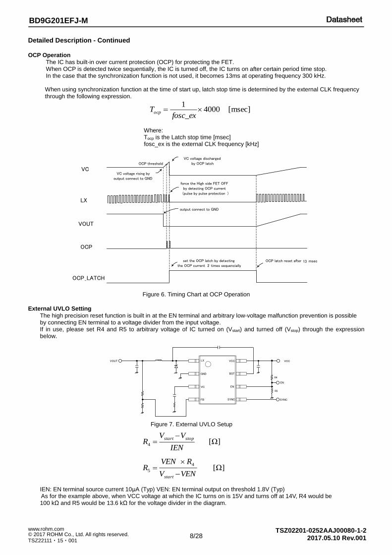
OCP Operation
The IC has built-in over current protection (OCP) for protecting the FET. When OCP is detected twice sequentially, the IC is turned off, the IC turns on after certain period time stop. In the case that the synchronization function is not used, it becomes 13ms at operating frequency 300 kHz. When using synchronization function at the time of start up, latch stop time is determined by the external CLK frequency through the following expression.
Where: Tocp is the Latch stop time [msec]
fosc_ex is the external CLK frequency [kHz]
Figure 6. Timing Chart at OCP Operation
External UVLO Setting
The high precision reset function is built in at the EN terminal and arbitrary low-voltage malfunction prevention is possible by connecting EN terminal to a voltage divider from the input voltage. If in use, please set R4 and R5 to arbitrary voltage of IC turned on (Vstart) and turned off (Vstop) through the expression below.
VCCVOUT
EN
LX
GND
VC
FB
VCC
BST
EN
SYNC SYNC
R4
R5
IEN: EN terminal source current 10μA (Typ) VEN: EN terminal output on threshold 1.8V (Typ) As for the example above, when VCC voltage at which the IC turns on is 15V and turns off at 14V, R4 would be 100 kΩ and R5 would be 13.6 kΩ for the voltage divider in the diagram.
VC
LX
VOUT
OCP
OCP _ LATCH
set the OCP latch by detecting the OCP current 2 times sequencially
output connect to GND
OCP latch reset after 13 msec
force the High side FET OFF by detecting OCP current ( pulse by pulse protection )
VC voltage discharged by OCP latch OCP threshold
VC voltage rising by output connect to GND
Figure 7. External UVLO Setup
]Ω[4 IEN
VVR
stopstart
]Ω[ 4
5 VENV
RVENR
start
]msec[40001
fosc_ex
Tocp

9/28
BD9G201EFJ-M
© 2017 ROHM Co., Ltd. All rights reserved. www.rohm.com
TSZ22111・15・001
TSZ02201-0252AAJ00080-1-2 2017.05.10 Rev.001
EN
0.8V
ErrorAMP
VCC
LX
REFUVLO
OFF
SoftStart
ON/OFF
GND
+
-+
FB
BST
TSD
shutdown
VC
Current Sense AMP
VOUT
SYNC
Oscillator
+
-
REG
MaxdutyLogic
10μA
+-1.8V
Nch FET SW
ENUVLO
CHG
OCP
OFF
MAX:4.9V
MAX:100uAΣ
R QS
Current Sense
Detailed Description - Continued
The countermeasure of voltage generation over output voltage in less than 4.9 V output voltage application
IC produces at most 100μA to the output via LX terminal from BST terminal which is drive power source terminal at the following condition
Output of IC can generate at 4.9V max from BST voltage, so according to output voltage setting, output voltage is greater than setting output voltage. In order to prevent over 100μA load in output or set a resistance level that feedback resister current is more than 100μA.
[Conditions] IC internal regulator is operating when switching is no operation. For example, input voltage is less than internal UVLO threshold, EN terminal voltage is condition of internal REG ON.
Figure 8. Current Path at the Time of the SW off and Internal REG ON

10/28
BD9G201EFJ-M
© 2017 ROHM Co., Ltd. All rights reserved. www.rohm.com
TSZ22111・15・001
TSZ02201-0252AAJ00080-1-2 2017.05.10 Rev.001
0
10
20
30
40
50
60
70
80
0 200 400 600 800 1000 1200 1400 1600
Tj [℃
]
Output Current [mA]
Detailed Description - Continued
LowDrop Out Operation
For the BST terminal charge that is the drive voltage of the High-side Nch FET, input and output voltage limit is set by MaxDuty. The IC has two operation modes: Steady operation mode and MaxDuty mode, to cope with wide duty output. When the IC is in steady operation mode, FET is switching every period. When the IC is in MaxDuty mode, after ON pulse continue 8, FET is forced off in 700ns.
Operation Duty is calculated as follows by input and output voltage to use and a load.
MaxDuty is calculated as follows by forced-off time (Typ: 300ns) and operating frequency.
In the case of 300 kHz operating frequency where the SYNC terminal is not used, MaxDuty for steady operation is 91%. If duty requirement is beyond this level, then shift to MaxDuty mode.
During MaxDuty mode, the IC is enabled to output 100% duty for 8 periods of internal CLK and exists a forced-off section of 700nsec. MaxDuty in the MaxDuty mode is expressed by the following equation.
In MaxDuty mode, switching operation does not occur every period, so the inductor ripple current and output ripple voltage become bigger than steady operation. Output voltage drops in the case of duty is higher than Don_max2.
MinDuty
There are output voltage restrictions by MinDuty. The MinDuty required is as follows with worst min on time (200nsec).
Heat generation for the Light-Load
For the light-load, Pre-charge Nch FET of 10Ω (typ) in this IC pulls out charge into GND, and BST capacitor is charged. When Pre-charge Nch FET pulls out charge, this IC has a loss by ON resistance 10Ω of Pre-charge Nch FET and the
flowing current. The loss and heat generation may be increased with the condition of high input voltage, high output voltage and low
inductance value. Confirmation of efficiency and heat generation for the light-load is recommended. When the heat generation for the light-load rises high, high inductance value is recommended. The heat generation is decreased by dropping down the ripple current.
%100
IOUTRVCC
VOUTDon
onH
%1003001max oscfnDon_
%1008
70012max
oscfn
Don_
%100200min oscfnDon_
Figure 9. Current Passes when Light-Load
Figure 10. Junction Temperature vs Output Current (VCC =24V, Vout= 12V)
(Rohm Board (4layers 40mm x 40mm) )
Pre-chargeNch FET
VOUT
VCC
LX
High-sideNch FET
L= 15µH
L= 22µH
L= 33µH L= 47µH
11/28
BD9G201EFJ-M
© 2017 ROHM Co., Ltd. All rights reserved. www.rohm.com
TSZ22111・15・001
TSZ02201-0252AAJ00080-1-2 2017.05.10 Rev.001
0.0
0.1
0.2
0.3
0.4
0.5
0.6
0.7
0.8
0.9
1.0
-60 -40 -20 0 20 40 60 80 100120
Sta
nd
by C
urr
en
t I s
t[µ
A]
Temperature [˚C]
0.0
0.5
1.0
1.5
2.0
-60 -40 -20 0 20 40 60 80 100 120
Inp
ut
Cir
cu
it C
urr
en
tI C
C[m
A]
Temperature [˚C]
3.0
3.2
3.4
3.6
3.8
4.0
4.2
4.4
4.6
4.8
5.0
-60 -40 -20 0 20 40 60 80 100 120
UV
LO
Th
res
ho
ld V
uv
[V]
Temperature [˚C]
0.0
0.5
1.0
1.5
2.0
0 5 10 15 20 25 30 35 40 45O
pe
rati
ng
Cu
rre
nt
I CC
[mA
]
VCC [V]
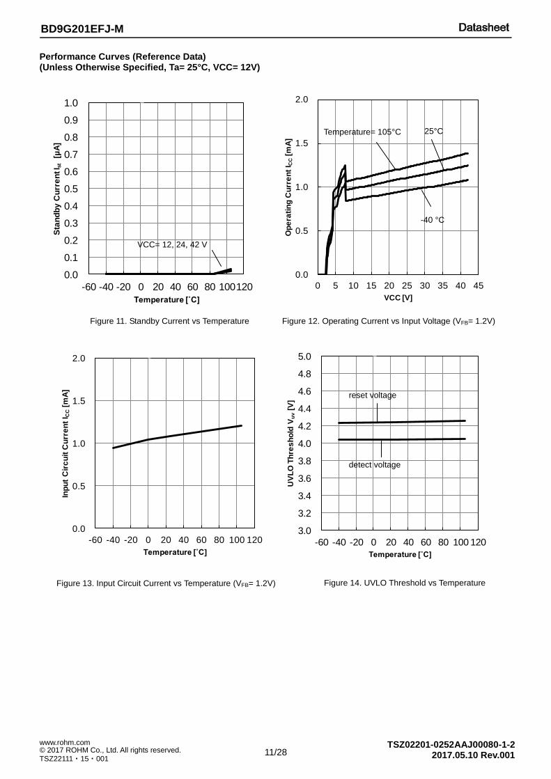
Performance Curves (Reference Data) (Unless Otherwise Specified, Ta= 25°C, VCC= 12V)
Figure 11. Standby Current vs Temperature
Figure 12. Operating Current vs Input Voltage (VFB= 1.2V)
Figure 13. Input Circuit Current vs Temperature (VFB= 1.2V) Figure 14. UVLO Threshold vs Temperature
Temperature= 105°C 25°C
-40 °C
VCC= 12, 24, 42 V
reset voltage
detect voltage

12/28
BD9G201EFJ-M
© 2017 ROHM Co., Ltd. All rights reserved. www.rohm.com
TSZ22111・15・001
TSZ02201-0252AAJ00080-1-2 2017.05.10 Rev.001
250
260
270
280
290
300
310
320
330
340
350
-60 -40 -20 0 20 40 60 80 100 120
Fre
qu
en
cy f
osc
[kH
z]
Temperature [˚C]
0.790
0.792
0.794
0.796
0.798
0.800
0.802
0.804
0.806
0.808
0.810
-60 -40 -20 0 20 40 60 80 100120
FB
Th
res
ho
ld V
FB
[V]
Temperature [˚C]
0.790
0.792
0.794
0.796
0.798
0.800
0.802
0.804
0.806
0.808
0.810
0 5 10 15 20 25 30 35 40 45
FB
Th
res
ho
ld V
FB
[V]
VCC [V]
90
92
94
96
98
100
-60 -40 -20 0 20 40 60 80 100 120M
ax
Du
ty D
max
[%]
Temperature [˚C]
Performance Curves (Reference Data) - Continued
Figure 15. Frequency vs Temperature
Figure 16. MaxDuty vs Temperature
Figure 17. FB Threshold vs Temperature
Figure 18. FB Threshold vs Input Voltage

13/28
BD9G201EFJ-M
© 2017 ROHM Co., Ltd. All rights reserved. www.rohm.com
TSZ22111・15・001
TSZ02201-0252AAJ00080-1-2 2017.05.10 Rev.001
0
2
4
6
8
10
12
14
16
-60 -40 -20 0 20 40 60 80 100 120
So
ftS
tart
Tim
e t
so
ft[m
se
c]
Temperature [˚C]
0
5
10
15
20
-60 -40 -20 0 20 40 60 80 100 120
Pre
ch
arg
e F
ET
Re
sis
tan
ce
[mΩ
]
Temperature [˚C]
0
50
100
150
200
250
300
-60 -40 -20 0 20 40 60 80 100 120H
igh
Sid
e F
ET
Re
sis
tan
ce
[m
Ω]
Temperature [˚C]
0
1
2
3
4
5
-60 -40 -20 0 20 40 60 80 100 120
OC
P D
ete
ct
Cu
rren
t [A
]
Temperature [˚C]
Performance Curves (Reference Data) - Continued
Figure 19. Soft Start Time vs Temperature
Figure 20. High Side FET Resistance vs Temperature
Figure 21. Precharge FET Resistance vs Temperature
Figure 22. OCP Detect Current vs Temperature
14/28
BD9G201EFJ-M
© 2017 ROHM Co., Ltd. All rights reserved. www.rohm.com
TSZ22111・15・001
TSZ02201-0252AAJ00080-1-2 2017.05.10 Rev.001
1.5
1.6
1.7
1.8
1.9
2.0
-60 -40 -20 0 20 40 60 80 100 120
EN
UV
LO
Th
res
ho
ld V
EN
UV
LO
[V]
Temperature [˚C]
9.0
9.2
9.4
9.6
9.8
10.0
10.2
10.4
10.6
10.8
11.0
-60 -40 -20 0 20 40 60 80 100120E
N U
VL
O S
ou
rce
Cu
rre
nt I E
N[µ
A]
Temperature [˚C]
Performance Curves (Reference Data) – Continued
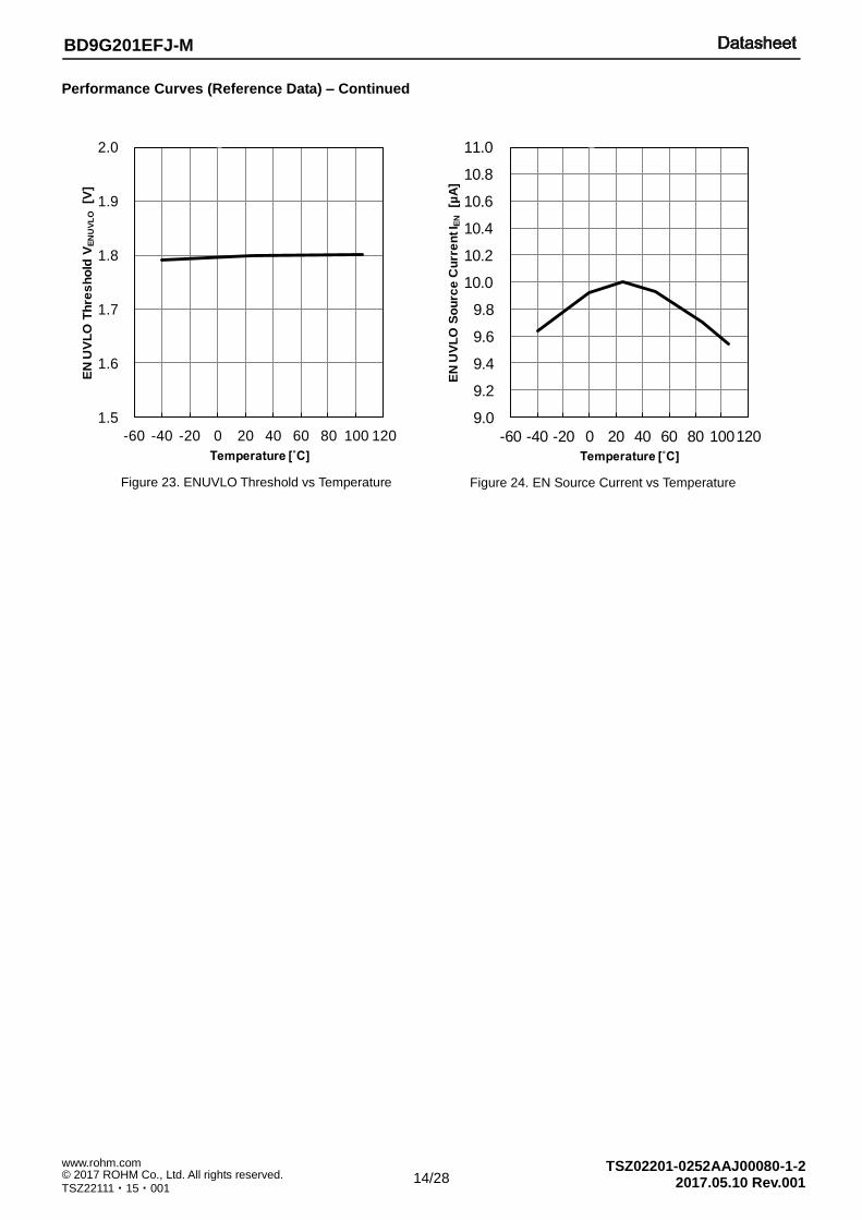
Figure 23. ENUVLO Threshold vs Temperature
Figure 24. EN Source Current vs Temperature

15/28
BD9G201EFJ-M
© 2017 ROHM Co., Ltd. All rights reserved. www.rohm.com
TSZ22111・15・001
TSZ02201-0252AAJ00080-1-2 2017.05.10 Rev.001
0
10
20
30
40
50
60
70
80
90
100
1 10 100 1000 10000
Effi
cie
ncy
[%]
IOUT [mA]
VCC=36V
VCC=24V
VCC=12V
VCC=42V
Reference Characteristics of Typical Application Circuits
VCCVOUT
0.01μF
EN
LX
GND
VC
FB
VCC
BST
EN
SYNC SYNC
CVCC
: 10µF/50V
COUT
: 47µF/16V
0.1µF
160kΩ
5V/1.5A
R4
R5
30kΩ 4.7kΩ
D1
L1: 22µH
Parts : L1 :TDK CLF12577NIT - 220M 22μH
CVCC :murata GRM32ER71H106K 10μF / 50V
COUT :murata GRM32EB31C476K 47μF / 16V
D1 :Rohm RB050L-60
Figure 25. Typical Application Circuits
Figure 26. Efficiency vs IOUT

16/28
BD9G201EFJ-M
© 2017 ROHM Co., Ltd. All rights reserved. www.rohm.com
TSZ22111・15・001
TSZ02201-0252AAJ00080-1-2 2017.05.10 Rev.001
Reference Characteristics of Typical Application Circuits - Continued
Figure 27. Frequency Characteristics (IOUT= 0.5A)
Figure 29. Startup Waveform (IOUT= 0.5A)
Figure 30. Shutdown Waveform (IOUT= 0.5A)
EN 5V/div
LX 10V/div
Input Current 200mA/div
VOUT 2V/div
EN 5V/div
LX 10V/div
Input Current 200mA/div
VOUT 2V/div
2msec/div 2msec/div
Phase
Gain
Figure 28. Frequency Characteristics (IOUT= 1.5A)
Phase
Gain

17/28
BD9G201EFJ-M
© 2017 ROHM Co., Ltd. All rights reserved. www.rohm.com
TSZ22111・15・001
TSZ02201-0252AAJ00080-1-2 2017.05.10 Rev.001
Application Components Selecting Method
(1) Inductor Shielded type that meets the current rating (current value from the Ipeak below), with low DCR (Direct Current Resistance element) is recommended. The value of inductor has an effect in the inductor ripple current which causes the output ripple. In the same formula below, this ripple current can be made small with a large value L of the inductor or as high as the switching frequency. Peak current of internal FET is needed to be lower than OCP threshold 2.0A (min).
Ipeak= Iout + ⊿ IL/2 [A] (1)
Where:
⊿ IL is the Inductor ripple current, f is switching frequency
For design value of inductor ripple current, please carry out design tentatively with about 20% to 50% of the maximum output current of the IC. The minimum value of inductance is shown in the following figure. Inductor is selected over the value of the graph.
When current that exceeds the inductor rating flows in to the inductor, the inductor causes a magnetic saturation which in turn causes a decline in efficiency and output oscillation. Please choose a inductor with a sufficient margin so that peak current does not exceed rating current of the inductor.
Δ IL
⊿ IL= x x [A] (2)
Figure 31. Inductor Current
L
Vin-Vout
Vin
Vout
f
1
02468101214161820222426283032343638404244464850
0 5 10 15 20 25 30 35 40
L [u
H]
Output Voltage [V]
Figure 32. Output Voltage vs inductance (min)

18/28
BD9G201EFJ-M
© 2017 ROHM Co., Ltd. All rights reserved. www.rohm.com
TSZ22111・15・001
TSZ02201-0252AAJ00080-1-2 2017.05.10 Rev.001
Application Components Selecting Method - Continued
(2) Input Capacitor
This IC needs an input decoupling capacitor. It is recommended a low ESR ceramic capacitor over 2.2μF.
The capacitance is selected considering temperature characteristics and bias voltage effect.
The input ripple voltage is determined by input capacitance (CIN). Because the IC input voltage is decreased, consider
input voltage range including ripple voltage. The input ripple voltage is estimated by the following.
Please notice that frequency is 1/8 times in maxduty mode when the difference between input voltage and output
voltage is small. Please refer to Detailed Description for the condition of maxduty mode.
The input capacitance has a sufficient value that keep input voltage in the recommended range.
Please confirm the characteristic of RMS ripple current – temperature.
RMS ripple current (IRMS) is following.
IRMS has a maximum value when VIN = 2 x VOUT
Choose an input capacitor that have enough temperature margin at the IRMS.
(3) Output Capacitor In order to reduce output ripple, a ceramic capacitor of low ESR is recommended. Also, for capacitor rating, take into consideration the DC bias characteristics. Use a capacitor with maximum rating of sufficient margin with respect to the output voltage. Output ripple voltage is obtained through the following formula.
Please set the value within allowable ripple voltage.
Confirm rush current(Irush) of the start up because the output capacitance has an effect of Irush.
Irush is estimated in the following.
Where:
Tsoftstart is soft start time fosc is inner frequency 300kHz
fosc_ex is SYNC frequency (If the SYNC function is not used, fosc_ex equals to fosc)
IOUTstart is output current when IC is start up.
At least, It is required that Irush is less than 2A that is minimum value of OCP threshold.
The rush current is added the current caused by ERROR AMP delay actually.
Please confirm that start up rush current is lower than 2A.
Vpp = ⊿ IL x + ⊿ IL x RESR [V] (6) 2π x f x COUT
1
)( (max)(max)
(max)RESRIOUT
VCCfCIN
VOUTIOUTVin
[Vp-p] (3)
VIN
VOUT
VIN
VOUTIOUTIRMS 1 [ARMS] (4)
2
IOUTIRMS [ARMS] (5)
start
oscsoftstart
exosc
rush IOUTILfT
fVOUTCOUTI
_ [A] (7)

19/28
BD9G201EFJ-M
© 2017 ROHM Co., Ltd. All rights reserved. www.rohm.com
TSZ22111・15・001
TSZ02201-0252AAJ00080-1-2 2017.05.10 Rev.001
Application Components Selecting Method - Continued (4) Output Voltage Setting
The ERROR AMP internal reference voltage is 0.8V. Output voltage is determined by next formula.
(5) Bootstrap Capacitor
Please connect a 0.1µF (Ceramic Capacitor) between BST and LX pin. Because the absolute rating between BST-LX becomes 7V, 10V or more are recommended.
(6) About the adjustment of DC / DC Converter Frequency Characteristics Role of phase compensation element C1, C2, R3 Stability and responsiveness of the loop are controlled through the VC terminal. The combination of zero and pole that determines the stability and responsiveness is adjusted through the combination of resistor and capacitor connected in series to the VC terminal. The DC Gain of the Voltage Feedback Loop can be calculated using the following formula.
Here, VFB is the Feedback Voltage (0.8V). AEA is the Voltage Gain of Error amplifier (Typ: 80dB), GCS is the Trans-conductance of Current Detect (Typ: 10A / V), and RI is the Output Load Resistance value. There are 2 poles in the control loop of this DC / DC. The first occurs in the output resistance of phase compensation capacitor (C1) and error amplifier, the other one occurs in the output capacitor and load resistor. These poles appear in the frequency written below.
GEA is the trans-conductance of Error amplifier (Typ: 220µA / V).
Figure 33. Voltage Feedback Resistance Setting Method
VREF 0.8 V
VOUT
ERROR AMP R1
R2
FB VOUT = x 0.8 [V] (8) R2
(R1 + R2)
GEA fp1 =
2π x C1 x AEA
1 fp2 =
2π x COUT x RI
VCC
C1
EN
LX
GND
VC
FB
VCC
BST
EN
SYNC SYNC
R3
C2
Vout
Figure 34. Phase Compensation Element
VFB Adc = RI x GCS x AEA x
Vout

20/28
BD9G201EFJ-M
© 2017 ROHM Co., Ltd. All rights reserved. www.rohm.com
TSZ22111・15・001
TSZ02201-0252AAJ00080-1-2 2017.05.10 Rev.001
Application Components Selecting Method - Continued This control loop has one zero. With the zero which occurs because of phase compensation capacitor C1 and phase compensation resistor R3, the frequency as shown below appears.
Also, if in this control loop the output capacitor is large, and that the ESR (RESR) is also large, has additional zero. This ESR zero that occurs due to ESR of output capacitor and its capacitance can be calculated as follows.
(fZESR : Zero frequency of ESR) In this
case, the 3rd pole is determined
with the 2nd phase compensation capacitor (C2) and phase correction resistor
(R3) is used in order to correct the ESR zero results in the loop gain. This pole exists in the frequency shown below. (fp3 : Pole frequency that corrects fZESR) The target of phase compensation design is to acquire necessary band and phase margin. It set that cross-over frequency (bandwidth):fc at which loop gain of the return loop becomes “0” . When the cross-over frequency becomes low, power supply fluctuation response, load response, etc worsens. when cross-over frequency becomes high, loop of phase margin becomes decrease. In order to ensure the phase margin, cross-over frequency needs to set 1/20 or below of the switching frequency.
Selection method of Phase Compensation constant is shown below.
1. Phase compensation resistor (R3) is selected in order to set the desired cross-over frequency. Calculation of R3 is done using the formula below.
2. Select phase compensation capacitor (C1). By matching the zero of compensation to 1/4 and below of the cross-over frequency, sufficient phase margin can be acquired. C1 can be calculated using the following formula.
3. Examination whether the second phase compensation capacitor C2 is necessary or not is done. If the ESR zero of the output capacitor is smaller than half of the switching frequency, a second phase compensation capacitor is necessary. In other words, it is the case wherein the condition below happens:
In this case, add a second phase compensation capacitor C2, and match the frequency of the third pole fp3 to the frequency of ESR zero. C2 can be acquired using the following formula.
1 1 fz =
2π x C1 x R3
R3 C2 2
1 3 fp
x x =
π
GCS GEA
fc COUT 2 x
x
x x =
π
VFB
Vout R3
fc R3 2
4 C1
x x π >
R3
RESR COUT C2
x
RESR COUT 2
1 fs
x x π <
2
1 fZESR =
2π x COUT x RESR
21/28
BD9G201EFJ-M
© 2017 ROHM Co., Ltd. All rights reserved. www.rohm.com
TSZ22111・15・001
TSZ02201-0252AAJ00080-1-2 2017.05.10 Rev.001
Power Dissipation Estimate The following formulas show how to estimate the device power dissipation under continuous mode operations. They should not be used if the device is working in the discontinuous conduction mode. IC internal loss is shown below.
1) Conduction loss:Pcon= IOUT2 x RonH x VOUT / VCC
2) Switching loss:Psw= 19×10-9
x VCC x IOUT x fsw
3) Gate charge loss:Pgc= 9.0×10⁻⁹
x fsw
4) Quiescent current loss:Pq= ICC x VCC
IOUT is the output current , RonH is the on-resistance of the high-side NchFET, VOUT is the output voltage. VCC is the input voltage, fsw is the switching frequency. Power dissipation of IC is the sum of above dissipation, and shown below. Pd= Pcon + Psw + Pgc + Pq Tj is shown below. Tj= Ta + θja x Pd The junction temperature is not more than Tjmax =150°C, so temperature design is needed sufficient margin.

22/28
BD9G201EFJ-M
© 2017 ROHM Co., Ltd. All rights reserved. www.rohm.com
TSZ22111・15・001
TSZ02201-0252AAJ00080-1-2 2017.05.10 Rev.001
PCB Layout Layout is a critical portion of a good power supply design. Here are several signals paths that conduct fast changing currents or voltages that can interact with stray inductance or parasitic capacitance to generate noise or degrade the power supply’s performance. To help eliminate these problems, the VCC terminal should be bypassed to ground with a low ESR ceramic bypass capacitor. Care should be taken to minimize the loop area formed by the bypass capacitor, VCC terminal, and anode of the catch diode. The thermal pad should be connected to any internal PCB ground plane using multiple VIAs directly under the IC. The LX pin should be routed to the cathode of the catch diode and to the output inductor. Since the LX connection is the switching node, the catch diode and output inductor should be located close to the LX pin, and the area of the PCB conductor is minimized to prevent excessive capacitive coupling.
Figure 35. Reference Evaluation Board Pattern
LX
GND
VC
FB
VCC
BST
EN
SYNC
Output
Inductor Catch
Diode
Output
Capacitor
Input Bypass
Capacitor
CBST
Topside
Ground
Area
Compensation
Network
Resistor
Divider
VOUT
Route BST Capacitor
Trace on another layer to provide with wide path for
topside ground
Signal VIA
Thermal VIA
VCC
23/28
BD9G201EFJ-M
© 2017 ROHM Co., Ltd. All rights reserved. www.rohm.com
TSZ22111・15・001
TSZ02201-0252AAJ00080-1-2 2017.05.10 Rev.001
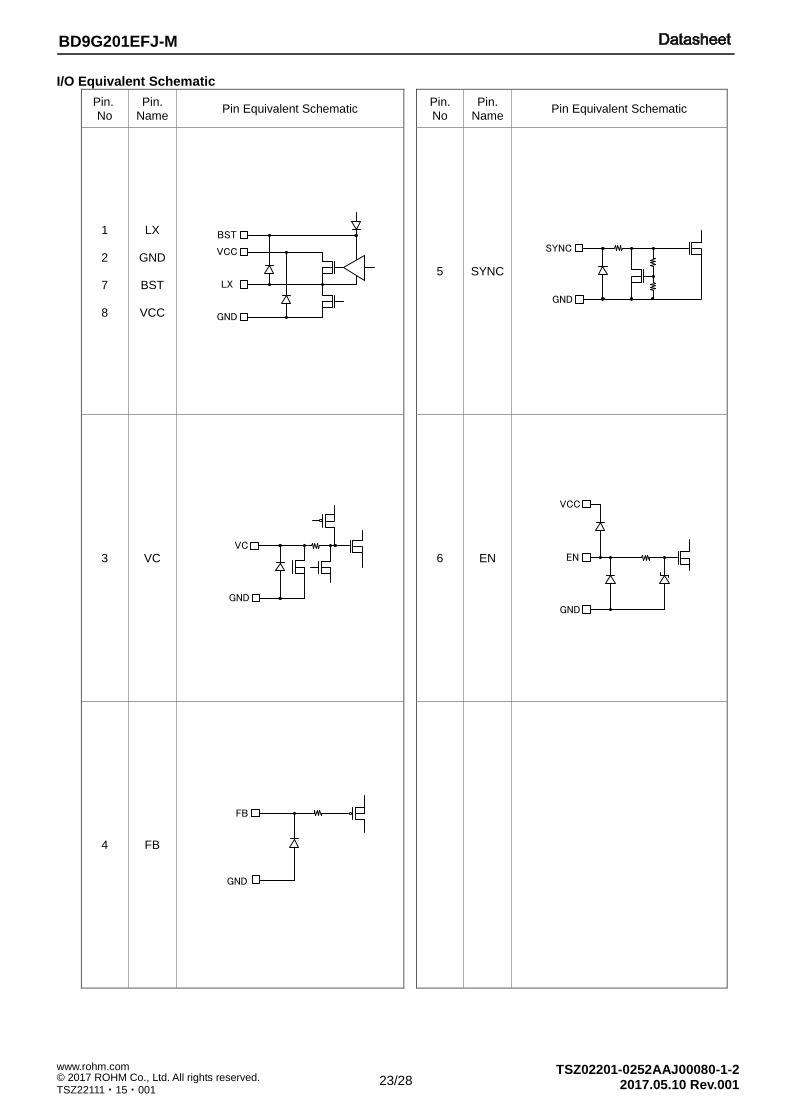
I/O Equivalent Schematic
Pin. No
Pin. Name
Pin Equivalent Schematic Pin. No
Pin. Name
Pin Equivalent Schematic
1
2
7
8
LX
GND
BST
VCC
BST
VCC
LX
GND
5 SYNC
SYNC
GND
3 VC VC
GND
6 EN
VCC
EN
GND
4 FB
FB
GND

24/28
BD9G201EFJ-M
© 2017 ROHM Co., Ltd. All rights reserved. www.rohm.com
TSZ22111・15・001
TSZ02201-0252AAJ00080-1-2 2017.05.10 Rev.001
Operational Notes
1. Reverse Connection of Power Supply
Connecting the power supply in reverse polarity can damage the IC. Take precautions against reverse polarity when connecting the power supply, such as mounting an external diode between the power supply and the IC’s power supply pins.
2. Power Supply Lines
Design the PCB layout pattern to provide low impedance supply lines. Furthermore, connect a capacitor to ground at all power supply pins. Consider the effect of temperature and aging on the capacitance value when using electrolytic capacitors.
3. Ground Voltage
Ensure that no pins are at a voltage below that of the ground pin at any time, even during transient condition. In addition, including transition phenomenon, it prevents all pin except GND pin from not becoming lower than GND pin voltage.
4. Ground Wiring Pattern
When using both small-signal and large-current ground traces, the two ground traces should be routed separately but connected to a single ground at the reference point of the application board to avoid fluctuations in the small-signal ground caused by large currents. Also ensure that the ground traces of external components do not cause variations on the ground voltage. The ground lines must be as short and thick as possible to reduce line impedance.
5. Thermal Consideration
Should by any chance the maximum junction temperature rating be exceeded the rise in temperature of the chip may result in deterioration of the properties of the chip. In case of exceeding this absolute maximum rating, increase the board size and copper area to prevent exceeding the maximum junction temperature rating.
6. Recommended Operating Conditions
These conditions represent a range within which the expected characteristics of the IC can be approximately obtained. The electrical characteristics are guaranteed under the conditions of each parameter.
7. Inrush Current
When power is first supplied to the IC, it is possible that the internal logic may be unstable and inrush current may flow instantaneously due to the internal powering sequence and delays, especially if the IC has more than one power supply. Therefore, give special consideration to power coupling capacitance, power wiring, width of ground wiring, and routing of connections.
8. Operation Under Strong Electromagnetic Field
Operating the IC in the presence of a strong electromagnetic field may cause the IC to malfunction.
9. Testing on Application Boards
When testing the IC on an application board, connecting a capacitor directly to a low-impedance output pin may subject the IC to stress. Always discharge capacitors completely after each process or step. The IC’s power supply should always be turned off completely before connecting or removing it from the test setup during the inspection process. To prevent damage from static discharge, ground the IC during assembly and use similar precautions during transport and storage.

25/28
BD9G201EFJ-M
© 2017 ROHM Co., Ltd. All rights reserved. www.rohm.com
TSZ22111・15・001
TSZ02201-0252AAJ00080-1-2 2017.05.10 Rev.001
Operational Notes – Continued
10. Inter-Pin Short and Mounting Errors
Ensure that the direction and position are correct when mounting the IC on the PCB. Incorrect mounting may result in damaging the IC. Avoid nearby pins being shorted to each other especially to ground, power supply and output pin. Inter-pin shorts could be due to many reasons such as metal particles, water droplets (in very humid environment) and unintentional solder bridge deposited in between pins during assembly to name a few.
11. Unused Input Pins
Input pins of an IC are often connected to the gate of a MOS transistor. The gate has extremely high impedance and extremely low capacitance. If left unconnected, the electric field from the outside can easily charge it. The small charge acquired in this way is enough to produce a significant effect on the conduction through the transistor and cause unexpected operation of the IC. So unless otherwise specified, unused input pins should be connected to the power supply or ground line.
12. Regarding the Input Pin of the IC
This monolithic IC contains P+ isolation and P substrate layers between adjacent elements in order to keep them isolated. P-N junctions are formed at the intersection of the P layers with the N layers of other elements, creating a parasitic diode or transistor. For example (refer to figure below):
When GND > Pin A and GND > Pin B, the P-N junction operates as a parasitic diode. When GND > Pin B, the P-N junction operates as a parasitic transistor.
Parasitic diodes inevitably occur in the structure of the IC. The operation of parasitic diodes can result in mutual interference among circuits, operational faults, or physical damage. Therefore, conditions that cause these diodes to operate, such as applying a voltage lower than the GND voltage to an input pin (and thus to the P substrate) should be avoided.
Figure 36. Example of Monolithic IC Structure
13. Ceramic Capacitor
When using a ceramic capacitor, determine the dielectric constant considering the change of capacitance with temperature and the decrease in nominal capacitance due to DC bias and others.
14. Area of Safe Operation (ASO)
Operate the IC such that the output voltage, output current, and the maximum junction temperature rating are all within the Area of Safe Operation (ASO).
15. Thermal Shutdown Circuit(TSD)
This IC has a built-in thermal shutdown circuit that prevents heat damage to the IC. Normal operation should always be within the IC’s maximum junction temperature rating. If however the rating is exceeded for a continued period, the junction temperature (Tj) will rise which will activate the TSD circuit that will turn OFF all output pins. When the Tj falls below the TSD threshold, the circuits are automatically restored to normal operation. Note that the TSD circuit operates in a situation that exceeds the absolute maximum ratings and therefore, under no circumstances, should the TSD circuit be used in a set design or for any purpose other than protecting the IC from heat damage.
16. Over Current Protection Circuit (OCP)
This IC incorporates an integrated overcurrent protection circuit that is activated when the load is shorted. This protection circuit is effective in preventing damage due to sudden and unexpected incidents. However, the IC should not be used in applications characterized by continuous operation or transitioning of the protection circuit.
N NP
+ P
N NP
+
P Substrate
GND
NP
+
N NP
+N P
P Substrate
GND GND
Parasitic
Elements
Pin A
Pin A
Pin B Pin B
B C
E
Parasitic
Elements
GNDParasitic
Elements
CB
E
Transistor (NPN)Resistor
N Region
close-by
Parasitic
Elements

26/28
BD9G201EFJ-M
© 2017 ROHM Co., Ltd. All rights reserved. www.rohm.com
TSZ22111・15・001
TSZ02201-0252AAJ00080-1-2 2017.05.10 Rev.001
Ordering Part Information
B D 9 G 2 0 1 E F J - ME 2
Part Number
Package EFJ : HTSOP-J8ES
Product Rank
M: for Automotive Packaging specification E2: Embossed tape and reel
Marking Diagram
HTSOP-J8ES (TOP VIEW)
D 9 G 2 0 1
Part Number Marking
LOT Number
1PIN MARK

27/28
BD9G201EFJ-M
© 2017 ROHM Co., Ltd. All rights reserved. www.rohm.com
TSZ22111・15・001
TSZ02201-0252AAJ00080-1-2 2017.05.10 Rev.001
Physical Dimension, Tape and Reel Information
Package Name HTSOP-J8ES
28/28
BD9G201EFJ-M
© 2017 ROHM Co., Ltd. All rights reserved. www.rohm.com
TSZ22111・15・001
TSZ02201-0252AAJ00080-1-2 2017.05.10 Rev.001
Revision History
Date Revision Changes
10.May.2017 001 Create new Rev.001

Notice-PAA-E Rev.003
© 2015 ROHM Co., Ltd. All rights reserved.
Notice
Precaution on using ROHM Products 1. If you intend to use our Products in devices requiring extremely high reliability (such as medical equipment
(Note 1),
aircraft/spacecraft, nuclear power controllers, etc.) and whose malfunction or failure may cause loss of human life, bodily injury or serious damage to property (“Specific Applications”), please consult with the ROHM sales representative in advance. Unless otherwise agreed in writing by ROHM in advance, ROHM shall not be in any way responsible or liable for any damages, expenses or losses incurred by you or third parties arising from the use of any ROHM’s Products for Specific Applications.
(Note1) Medical Equipment Classification of the Specific Applications
JAPAN USA EU CHINA
CLASSⅢ CLASSⅢ
CLASSⅡb CLASSⅢ
CLASSⅣ CLASSⅢ
2. ROHM designs and manufactures its Products subject to strict quality control system. However, semiconductor
products can fail or malfunction at a certain rate. Please be sure to implement, at your own responsibilities, adequate safety measures including but not limited to fail-safe design against the physical injury, damage to any property, which a failure or malfunction of our Products may cause. The following are examples of safety measures:
[a] Installation of protection circuits or other protective devices to improve system safety [b] Installation of redundant circuits to reduce the impact of single or multiple circuit failure
3. Our Products are not designed under any special or extraordinary environments or conditions, as exemplified below. Accordingly, ROHM shall not be in any way responsible or liable for any damages, expenses or losses arising from the use of any ROHM’s Products under any special or extraordinary environments or conditions. If you intend to use our Products under any special or extraordinary environments or conditions (as exemplified below), your independent verification and confirmation of product performance, reliability, etc, prior to use, must be necessary:
[a] Use of our Products in any types of liquid, including water, oils, chemicals, and organic solvents [b] Use of our Products outdoors or in places where the Products are exposed to direct sunlight or dust [c] Use of our Products in places where the Products are exposed to sea wind or corrosive gases, including Cl2,
H2S, NH3, SO2, and NO2
[d] Use of our Products in places where the Products are exposed to static electricity or electromagnetic waves [e] Use of our Products in proximity to heat-producing components, plastic cords, or other flammable items [f] Sealing or coating our Products with resin or other coating materials [g] Use of our Products without cleaning residue of flux (even if you use no-clean type fluxes, cleaning residue of
flux is recommended); or Washing our Products by using water or water-soluble cleaning agents for cleaning residue after soldering
[h] Use of the Products in places subject to dew condensation
4. The Products are not subject to radiation-proof design. 5. Please verify and confirm characteristics of the final or mounted products in using the Products. 6. In particular, if a transient load (a large amount of load applied in a short period of time, such as pulse. is applied,
confirmation of performance characteristics after on-board mounting is strongly recommended. Avoid applying power exceeding normal rated power; exceeding the power rating under steady-state loading condition may negatively affect product performance and reliability.
7. De-rate Power Dissipation depending on ambient temperature. When used in sealed area, confirm that it is the use in
the range that does not exceed the maximum junction temperature. 8. Confirm that operation temperature is within the specified range described in the product specification. 9. ROHM shall not be in any way responsible or liable for failure induced under deviant condition from what is defined in
this document.
Precaution for Mounting / Circuit board design 1. When a highly active halogenous (chlorine, bromine, etc.) flux is used, the residue of flux may negatively affect product
performance and reliability. 2. In principle, the reflow soldering method must be used on a surface-mount products, the flow soldering method must
be used on a through hole mount products. If the flow soldering method is preferred on a surface-mount products, please consult with the ROHM representative in advance.
For details, please refer to ROHM Mounting specification

Notice-PAA-E Rev.003
© 2015 ROHM Co., Ltd. All rights reserved.
Precautions Regarding Application Examples and External Circuits 1. If change is made to the constant of an external circuit, please allow a sufficient margin considering variations of the
characteristics of the Products and external components, including transient characteristics, as well as static characteristics.
2. You agree that application notes, reference designs, and associated data and information contained in this document
are presented only as guidance for Products use. Therefore, in case you use such information, you are solely responsible for it and you must exercise your own independent verification and judgment in the use of such information contained in this document. ROHM shall not be in any way responsible or liable for any damages, expenses or losses incurred by you or third parties arising from the use of such information.
Precaution for Electrostatic This Product is electrostatic sensitive product, which may be damaged due to electrostatic discharge. Please take proper caution in your manufacturing process and storage so that voltage exceeding the Products maximum rating will not be applied to Products. Please take special care under dry condition (e.g. Grounding of human body / equipment / solder iron, isolation from charged objects, setting of Ionizer, friction prevention and temperature / humidity control).
Precaution for Storage / Transportation 1. Product performance and soldered connections may deteriorate if the Products are stored in the places where:
[a] the Products are exposed to sea winds or corrosive gases, including Cl2, H2S, NH3, SO2, and NO2 [b] the temperature or humidity exceeds those recommended by ROHM [c] the Products are exposed to direct sunshine or condensation [d] the Products are exposed to high Electrostatic
2. Even under ROHM recommended storage condition, solderability of products out of recommended storage time period may be degraded. It is strongly recommended to confirm solderability before using Products of which storage time is exceeding the recommended storage time period.
3. Store / transport cartons in the correct direction, which is indicated on a carton with a symbol. Otherwise bent leads
may occur due to excessive stress applied when dropping of a carton. 4. Use Products within the specified time after opening a humidity barrier bag. Baking is required before using Products of
which storage time is exceeding the recommended storage time period.
Precaution for Product Label A two-dimensional barcode printed on ROHM Products label is for ROHM’s internal use only.
Precaution for Disposition When disposing Products please dispose them properly using an authorized industry waste company.
Precaution for Foreign Exchange and Foreign Trade act Since concerned goods might be fallen under listed items of export control prescribed by Foreign exchange and Foreign trade act, please consult with ROHM in case of export.
Precaution Regarding Intellectual Property Rights 1. All information and data including but not limited to application example contained in this document is for reference
only. ROHM does not warrant that foregoing information or data will not infringe any intellectual property rights or any other rights of any third party regarding such information or data.
2. ROHM shall not have any obligations where the claims, actions or demands arising from the combination of the Products with other articles such as components, circuits, systems or external equipment (including software).
3. No license, expressly or implied, is granted hereby under any intellectual property rights or other rights of ROHM or any third parties with respect to the Products or the information contained in this document. Provided, however, that ROHM will not assert its intellectual property rights or other rights against you or your customers to the extent necessary to manufacture or sell products containing the Products, subject to the terms and conditions herein.
Other Precaution 1. This document may not be reprinted or reproduced, in whole or in part, without prior written consent of ROHM.
2. The Products may not be disassembled, converted, modified, reproduced or otherwise changed without prior written consent of ROHM.
3. In no event shall you use in any way whatsoever the Products and the related technical information contained in the Products or this document for any military purposes, including but not limited to, the development of mass-destruction weapons.
4. The proper names of companies or products described in this document are trademarks or registered trademarks of ROHM, its affiliated companies or third parties.

DatasheetDatasheet
Notice – WE Rev.001© 2015 ROHM Co., Ltd. All rights reserved.
General Precaution 1. Before you use our Pro ducts, you are requested to care fully read this document and fully understand its contents.
ROHM shall n ot be in an y way responsible or liabl e for fa ilure, malfunction or acci dent arising from the use of a ny ROHM’s Products against warning, caution or note contained in this document.
2. All information contained in this docume nt is current as of the issuing date and subj ect to change without any prior
notice. Before purchasing or using ROHM’s Products, please confirm the la test information with a ROHM sale s representative.
3. The information contained in this doc ument is provi ded on an “as is” basis and ROHM does not warrant that all
information contained in this document is accurate an d/or error-free. ROHM shall not be in an y way responsible or liable for any damages, expenses or losses incurred by you or third parties resulting from inaccuracy or errors of or concerning such information.
Related Documents