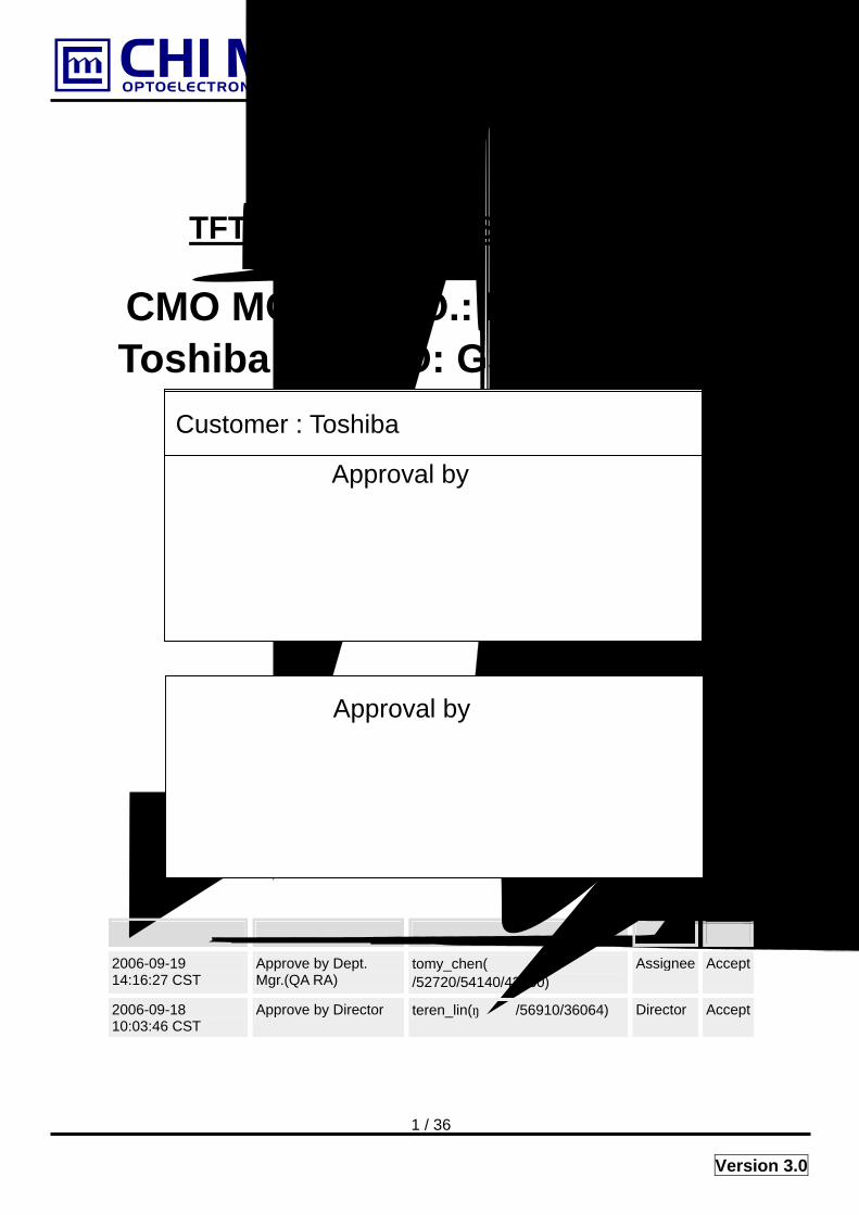
Doc No.: Issued Date: Aug. 29, 2006 Model No.: N150P5 -L04 Approval 1 / 36 Version 3.0 TFT LCD Approval Specification CMO MODEL NO.: N150P5 - L04 Toshiba Part NO: G33C0003S110 記錄 工作 審核 角色 投票 2006-09-19 14:16:27 CST Approve by Dept. Mgr.(QA RA) tomy_chen(陳永一 /52720/54140/43150) Assignee Accept 2006-09-18 10:03:46 CST Approve by Director teren_lin(林添仁/56910/36064) Director Accept Approval by Customer : Toshiba Approval by

Welcome message from author
This document is posted to help you gain knowledge. Please leave a comment to let me know what you think about it! Share it to your friends and learn new things together.
Transcript
Doc No.: Issued Date: Aug. 29, 2006
Model No.: N150P5 -L04
Approval
1 / 36 Version 3.0
TFT LCD Approval Specification
CMO MODEL NO.: N150P5 - L04 Toshiba Part NO: G33C0003S110
記錄 工作 審核 角色 投票
2006-09-19 14:16:27 CST
Approve by Dept. Mgr.(QA RA)
tomy_chen(陳永一/52720/54140/43150)
Assignee Accept
2006-09-18 10:03:46 CST
Approve by Director teren_lin(林添仁/56910/36064) Director Accept
Approval by
Customer : Toshiba
Approval by
Doc No.: Issued Date: Aug. 29, 2006
Model No.: N150P5 -L04
Approval
2 / 36 Version 3.0
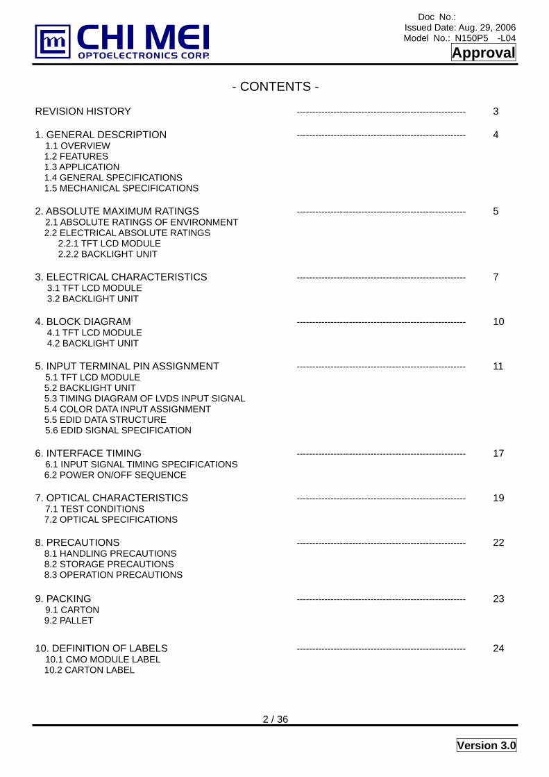
- CONTENTS - REVISION HISTORY ------------------------------------------------------- 3 1. GENERAL DESCRIPTION ------------------------------------------------------- 4 1.1 OVERVIEW 1.2 FEATURES 1.3 APPLICATION 1.4 GENERAL SPECIFICATIONS 1.5 MECHANICAL SPECIFICATIONS 2. ABSOLUTE MAXIMUM RATINGS ------------------------------------------------------- 5 2.1 ABSOLUTE RATINGS OF ENVIRONMENT 2.2 ELECTRICAL ABSOLUTE RATINGS 2.2.1 TFT LCD MODULE 2.2.2 BACKLIGHT UNIT 3. ELECTRICAL CHARACTERISTICS ------------------------------------------------------- 7
3.1 TFT LCD MODULE 3.2 BACKLIGHT UNIT
4. BLOCK DIAGRAM ------------------------------------------------------- 10
4.1 TFT LCD MODULE 4.2 BACKLIGHT UNIT
5. INPUT TERMINAL PIN ASSIGNMENT ------------------------------------------------------- 11 5.1 TFT LCD MODULE 5.2 BACKLIGHT UNIT 5.3 TIMING DIAGRAM OF LVDS INPUT SIGNAL 5.4 COLOR DATA INPUT ASSIGNMENT 5.5 EDID DATA STRUCTURE 5.6 EDID SIGNAL SPECIFICATION 6. INTERFACE TIMING ------------------------------------------------------- 17 6.1 INPUT SIGNAL TIMING SPECIFICATIONS 6.2 POWER ON/OFF SEQUENCE 7. OPTICAL CHARACTERISTICS ------------------------------------------------------- 19 7.1 TEST CONDITIONS 7.2 OPTICAL SPECIFICATIONS 8. PRECAUTIONS ------------------------------------------------------- 22 8.1 HANDLING PRECAUTIONS 8.2 STORAGE PRECAUTIONS 8.3 OPERATION PRECAUTIONS 9. PACKING ------------------------------------------------------- 23 9.1 CARTON 9.2 PALLET 10. DEFINITION OF LABELS ------------------------------------------------------- 24 10.1 CMO MODULE LABEL 10.2 CARTON LABEL
Doc No.: Issued Date: Aug. 29, 2006
Model No.: N150P5 -L04
Approval
3 / 36 Version 3.0
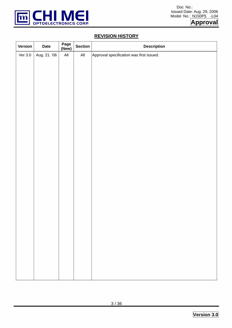
REVISION HISTORY
Version Date Page(New) Section Description
Ver 3.0
Aug. 21. ‘06
All
All
Approval specification was first issued.
Doc No.: Issued Date: Aug. 29, 2006
Model No.: N150P5 -L04
Approval
4 / 36 Version 3.0
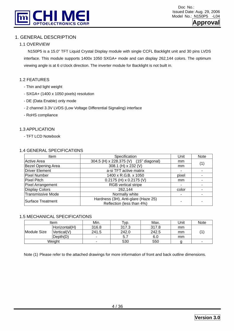
1. GENERAL DESCRIPTION 1.1 OVERVIEW
N150P5 is a 15.0” TFT Liquid Crystal Display module with single CCFL Backlight unit and 30 pins LVDS
interface. This module supports 1400x 1050 SXGA+ mode and can display 262,144 colors. The optimum
viewing angle is at 6 o’clock direction. The inverter module for Backlight is not built in.
1.2 FEATURES - Thin and light weight
- SXGA+ (1400 x 1050 pixels) resolution
- DE (Data Enable) only mode
- 2 channel 3.3V LVDS (Low Voltage Differential Signaling) interface
- RoHS compliance
1.3 APPLICATION - TFT LCD Notebook
1.4 GENERAL SPECIFICATI0NS Item Specification Unit Note
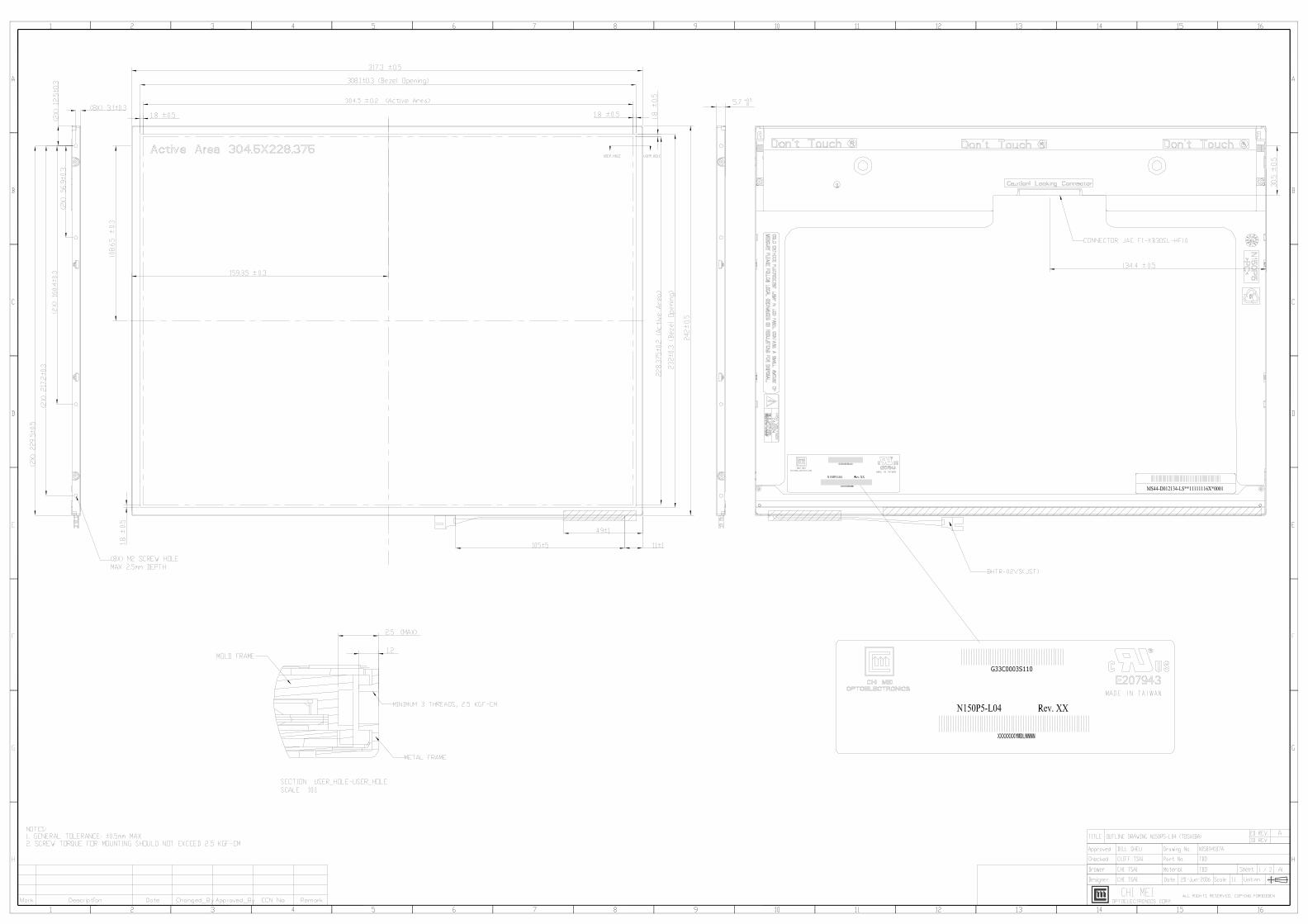
Active Area 304.5 (H) x 228.375 (V) (15” diagonal) mm Bezel Opening Area 308.1 (H) x 232 (V) mm (1)
Driver Element a-si TFT active matrix - - Pixel Number 1400 x R.G.B. x 1050 pixel - Pixel Pitch 0.2175 (H) x 0.2175 (V) mm - Pixel Arrangement RGB vertical stripe - - Display Colors 262,144 color - Transmissive Mode Normally white - -
Surface Treatment Hardness (3H), Anti-glare (Haze 25) Reflection (less than 4%) - -
1.5 MECHANICAL SPECIFICATIONS Item Min. Typ. Max. Unit Note
Horizontal(H) 316.8 317.3 317.8 mm Vertical(V) 241.5 242.0 242.5 mm Module Size Depth(D) - 5.7 6.0 mm
(1)
Weight - 530 550 g -
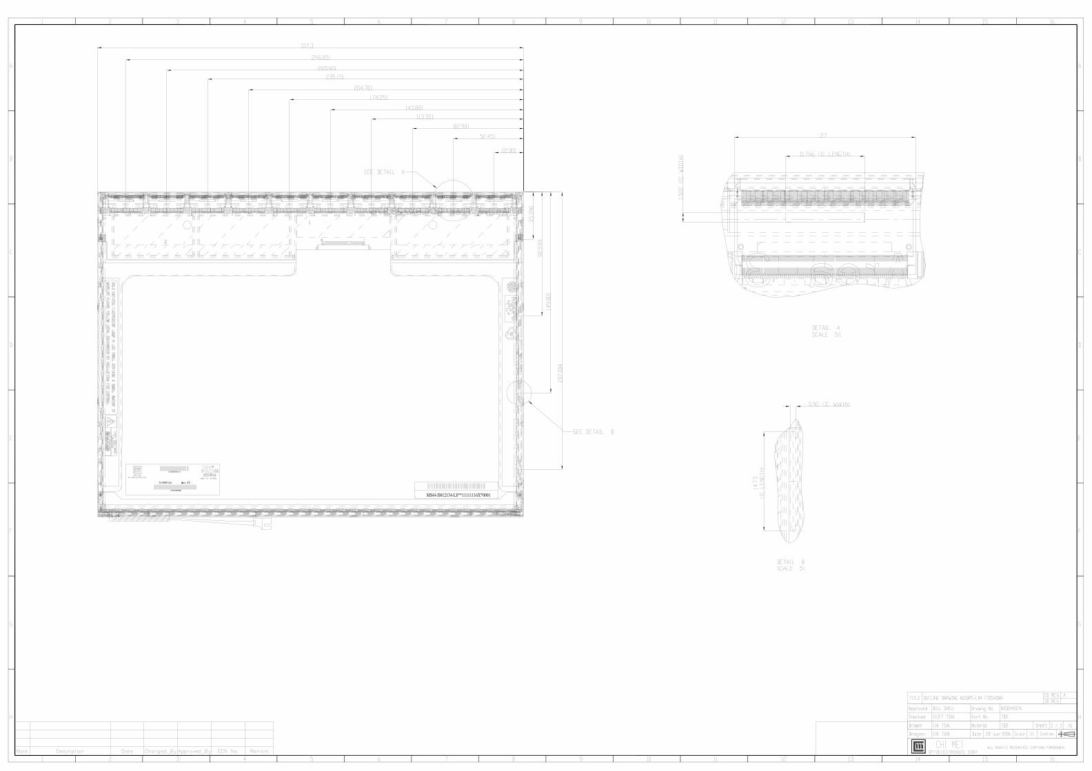
Note (1) Please refer to the attached drawings for more information of front and back outline dimensions.
Doc No.: Issued Date: Aug. 29, 2006
Model No.: N150P5 -L04
Approval
5 / 36 Version 3.0
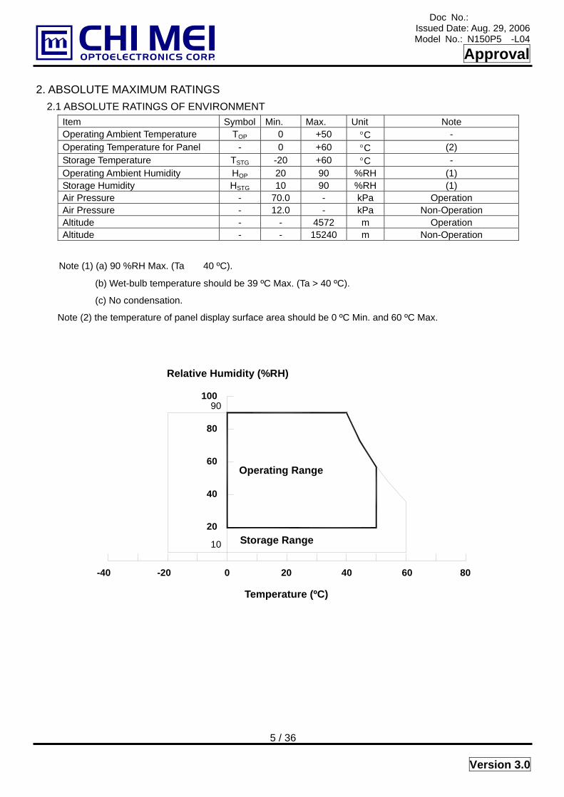
2. ABSOLUTE MAXIMUM RATINGS 2.1 ABSOLUTE RATINGS OF ENVIRONMENT
Item Symbol Min. Max. Unit Note Operating Ambient Temperature TOP 0 +50 °C - Operating Temperature for Panel - 0 +60 °C (2) Storage Temperature TSTG -20 +60 °C - Operating Ambient Humidity HOP 20 90 %RH (1) Storage Humidity HSTG 10 90 %RH (1) Air Pressure - 70.0 - kPa Operation Air Pressure - 12.0 - kPa Non-Operation Altitude - - 4572 m Operation Altitude - - 15240 m Non-Operation
Note (1) (a) 90 %RH Max. (Ta ≦ 40 ºC).
(b) Wet-bulb temperature should be 39 ºC Max. (Ta > 40 ºC).
(c) No condensation.
Note (2) the temperature of panel display surface area should be 0 ºC Min. and 60 ºC Max.
Relative Humidity (%RH)
Operating Range
Temperature (ºC)
100
8060 -20 400 20-40
90
80
40
60
20
10 Storage Range

Doc No.: Issued Date: Aug. 29, 2006
Model No.: N150P5 -L04
Approval
6 / 36 Version 3.0
2.2 ELECTRICAL ABSOLUTE RATINGS 2.2.1 TFT LCD MODULE
Value Item Symbol Min. Max. Unit Note
Power Supply Voltage Vcc -0.3 +4.0 V Logic Input Voltage VIN -0.3 Vcc+0.3 V (1)
2.2.2 BACKLIGHT UNIT Value Item Symbol Min. Max. Unit Note
Lamp Voltage VL - 2.5K VRMS (1), (2), IL = (6.0) mA Lamp Current IL 2.0 7.0 mARMSLamp Frequency FL 45 80 KHz (1), (2)
Note (1) Permanent damage to the device may occur if maximum values are exceeded. Function operation
should be restricted to the conditions described under Normal Operating Conditions.
Note (2) Specified values are for lamp (Refer to Section 3.2 for further information).
Doc No.: Issued Date: Aug. 29, 2006
Model No.: N150P5 -L04
Approval
7 / 36 Version 3.0
2.3 MECHANICAL RATINGS Item Test Conditions Note
Frequency Range 10~200Hz, 14.7m/s2 ( 1.5G) constant, 0.5Hrs each axis (X, Y, Z direction)
Non Operation Mechanical Vibration
Frequency Range10~200Hz, 4.9m/s2 ( 0.5G) constant, 0.5Hrs each axis (X, Y, Z direction)
Operation
2548m/s2 (260G), Pulse width 2ms, Half-Sine Wave, ±X, ±Y, ±Z direction, each 1 time
Operation & Non Operation
Mechanical Shock
686m/s2 (70G), Pulse width 11 ms, Half-Sine Wave, ±X, ±Y, ±Z direction, each 3 times.
Non Operation
No Destruction with the force 196 N (20 kgf, 16 mm in diameter) to the display surface at the vertical direction
Pressure Resistance
No Destruction with the force 294.2 N (30 kgf, 30 mm in diameter) to the back of the display surface at the vertical direction
Non Operation (1) Fig 2-3-1 (2) Fig 2-3-2 (3) Fig 2-3-3
Cable: No disconnection of cable to the 5 trial of 360o rotation. See a bent state of cable.
Strength of rotation force
Connector: No disconnection of cable to 10 trial of 180o rotation. See a bent state of cable. Soldering portion: 14.7N (1.5kgf), 1min
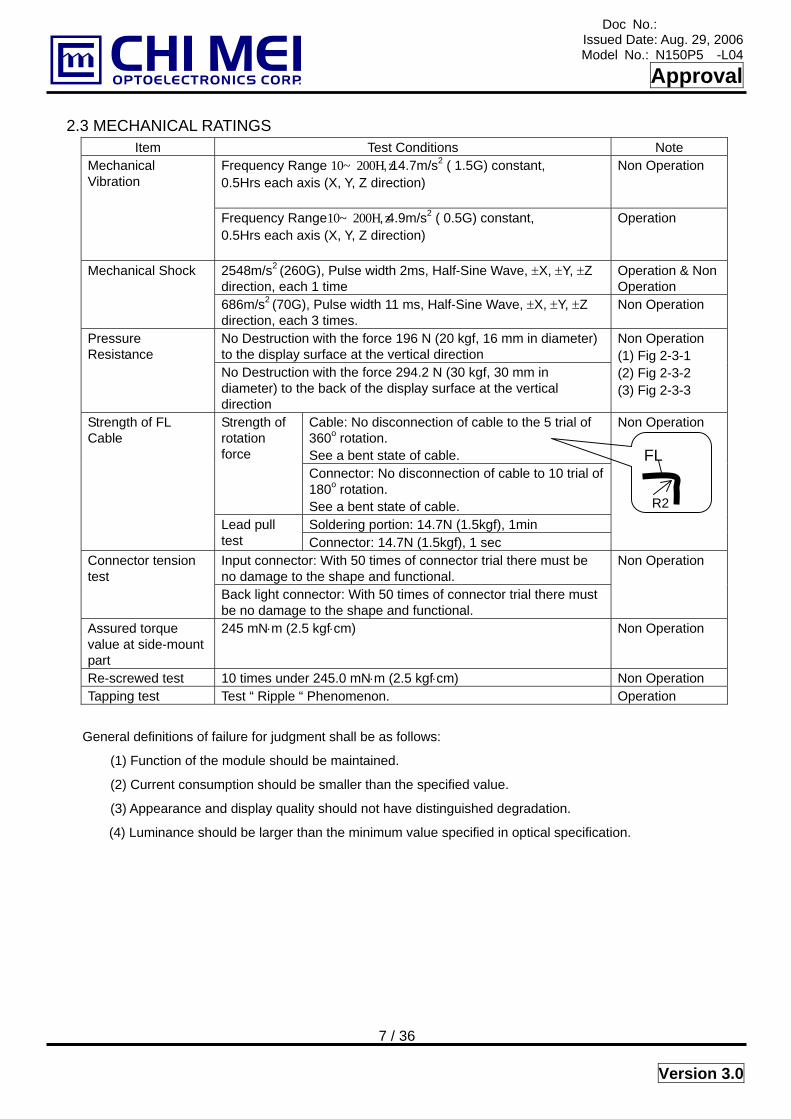
Strength of FL Cable
Lead pull test Connector: 14.7N (1.5kgf), 1 sec
Non Operation
Input connector: With 50 times of connector trial there must be no damage to the shape and functional.
Connector tension test
Back light connector: With 50 times of connector trial there must be no damage to the shape and functional.
Non Operation
Assured torque value at side-mount part
245 mN⋅m (2.5 kgf⋅cm) Non Operation
Re-screwed test 10 times under 245.0 mN⋅m (2.5 kgf⋅cm) Non Operation Tapping test Test “ Ripple “ Phenomenon. Operation
General definitions of failure for judgment shall be as follows:
(1) Function of the module should be maintained.
(2) Current consumption should be smaller than the specified value.
(3) Appearance and display quality should not have distinguished degradation.
(4) Luminance should be larger than the minimum value specified in optical specification.
FL
R2
Doc No.: Issued Date: Aug. 29, 2006
Model No.: N150P5 -L04
Approval
8 / 36 Version 3.0
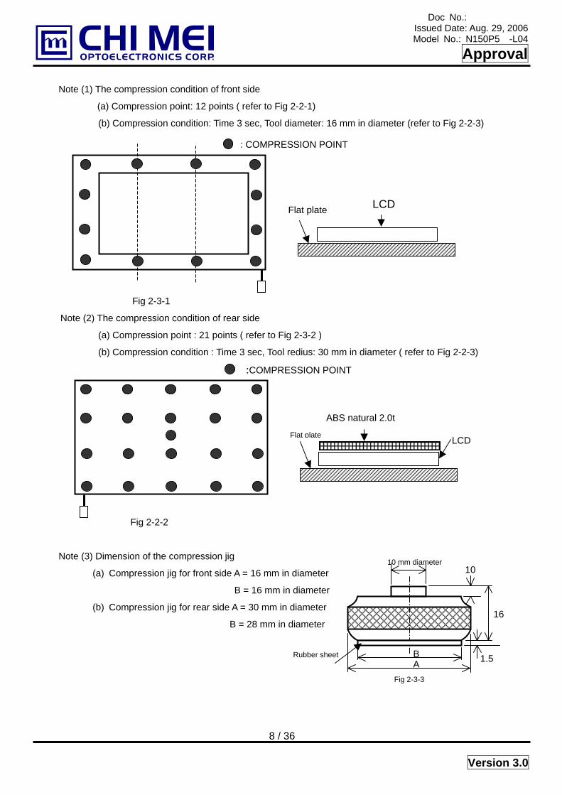
Note (1) The compression condition of front side
(a) Compression point: 12 points ( refer to Fig 2-2-1)
(b) Compression condition: Time 3 sec, Tool diameter: 16 mm in diameter (refer to Fig 2-2-3)
Fig 2-3-1
Note (2) The compression condition of rear side
(a) Compression point : 21 points ( refer to Fig 2-3-2 )
(b) Compression condition : Time 3 sec, Tool redius: 30 mm in diameter ( refer to Fig 2-2-3)
Fig 2-2-2
Note (3) Dimension of the compression jig
(a) Compression jig for front side A = 16 mm in diameter
B = 16 mm in diameter
(b) Compression jig for rear side A = 30 mm in diameter
B = 28 mm in diameter
Flat plate LCD
:COMPRESSION POINT
LCDFlat plate
ABS natural 2.0t
: COMPRESSION POINT
10 mm diameter
Fig 2-3-3
10
A B
16
1.5 Rubber sheet
Doc No.: Issued Date: Aug. 29, 2006
Model No.: N150P5 -L04
Approval
9 / 36 Version 3.0
2.4 OTHER RATING 2.4.1 STATIC ELECTRICITY PRESSURE RESISTANCE
Items Testing conditions Operation Non Operation
Contact discharge 150pF, 330 ohm ±10 kV ±10 kV
Air discharge 150pF, 330 ohm ±20 kV ±20 kV
ESD Acceptance Definition:
Temporary performance degradation. Recovery by operator is acceptable. No hardware failure.
2.4.2 SOUND NOISE There should be no uncomfortable noise.
Being used under whatever surrounds, when power on/off, the panel should not generate uncomfortable noise.
2.4.3 OPEN/SHORT
No smoke, no firery at any open/ short test
2.4.4 MTBF: 50000 Hours (except for backlight lamp)

Doc No.: Issued Date: Aug. 29, 2006
Model No.: N150P5 -L04
Approval
10 / 36 Version 3.0
3. ELECTRICAL CHARACTERISTICS 3.1 TFT LCD MODULE Ta = 25 ± 2 ºC
Value Parameter Symbol Min. Typ. Max. Unit Note
Power Supply Voltage Vcc 3.0 3.3 3.6 V - Ripple Voltage VRP - 50 - mV - Rush Current IRUSH - - 1.5 A (2)
White - 400 450 (3)a Black - 530 580 (3)b Power Supply Current 2V1H
lcc - 430 480
mA (3)c
“H” Level VIH - - +100 mV - Differential Input Voltage for LVDS Receiver Threshold “L” Level VIL -100 - - mV - Terminating Resistor RT - 100 - Ohm - Power per EBL WG PEBL - 3.42 - W (4) Note (1) The module should be always operated within above ranges.
Note (2) Measurement Conditions:
Vcc rising time is 470us
470us
+3.3V
GND
0.9Vcc
0.1Vcc
R1
(High to Low) (Control Signal)
+12V
SW Q2
C1
1uF
Vcc +3.3V
2SK1470
Q1 2SK1475
47K
R2
1K
VR1 47K C2
0.01uF
C3 1uF
FUSE (LCD Module Input)
Doc No.: Issued Date: Aug. 29, 2006
Model No.: N150P5 -L04
Approval
11 / 36 Version 3.0
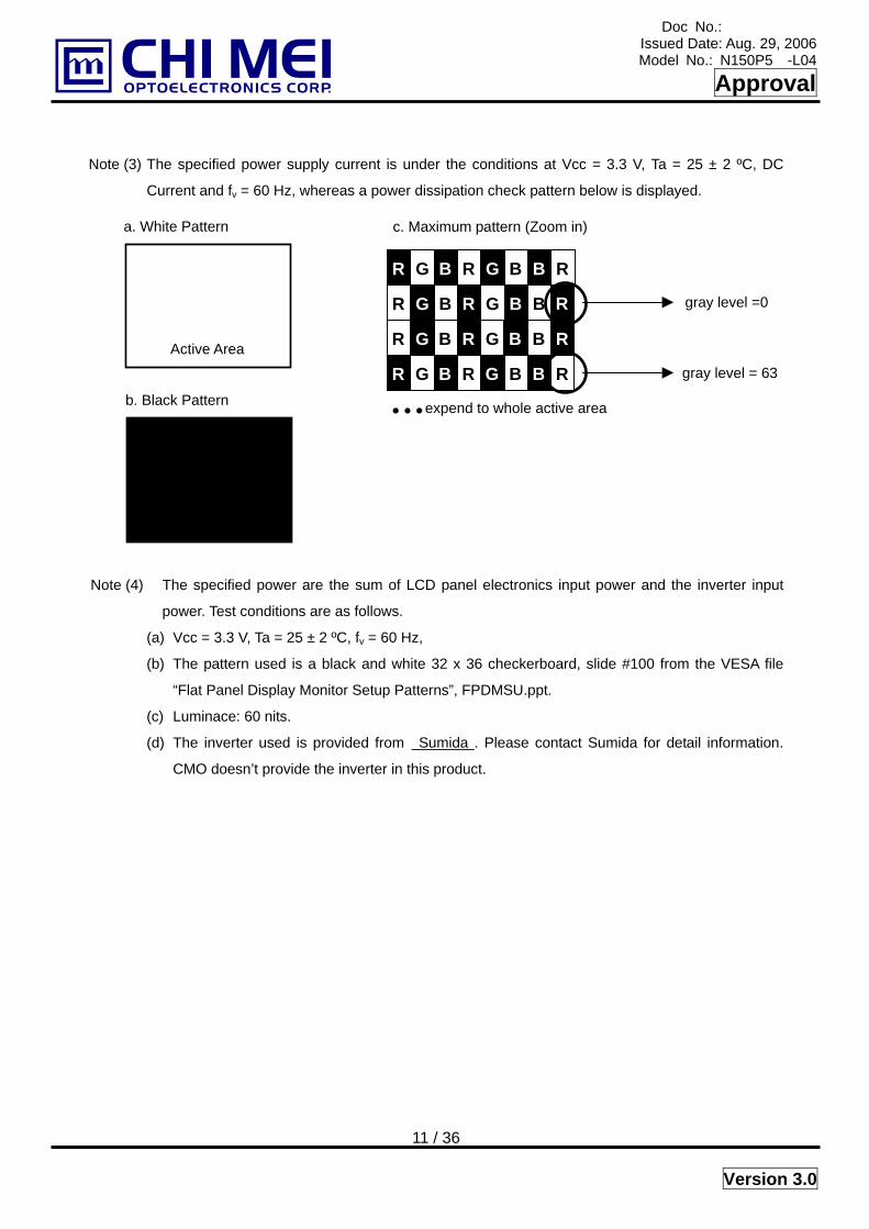
Note (3) The specified power supply current is under the conditions at Vcc = 3.3 V, Ta = 25 ± 2 ºC, DC
Current and fv = 60 Hz, whereas a power dissipation check pattern below is displayed.
Note (4) The specified power are the sum of LCD panel electronics input power and the inverter input
power. Test conditions are as follows.
(a) Vcc = 3.3 V, Ta = 25 ± 2 ºC, fv = 60 Hz,
(b) The pattern used is a black and white 32 x 36 checkerboard, slide #100 from the VESA file
“Flat Panel Display Monitor Setup Patterns”, FPDMSU.ppt.
(c) Luminace: 60 nits.
(d) The inverter used is provided from Sumida . Please contact Sumida for detail information.
CMO doesn’t provide the inverter in this product.
Active Area
a. White Pattern
b. Black Pattern
R
R
G
G
B
B
R
R
G
G
B
B
R
R
G
G
B
B
R
R
G
G
B
B
B
B
R
R
B
B
R
R
c. Maximum pattern (Zoom in)
…expend to whole active area
gray level =0
gray level = 63

Doc No.: Issued Date: Aug. 29, 2006
Model No.: N150P5 -L04
Approval
12 / 36 Version 3.0
3.2 MATERIAL LIST CONCERNING EMI REGULATIONS
(1) EMI Regulations: “N150P5-L04” which is assembled inside Toshiba’s Satellite model should be met to
the regulations as below:
CISPR: Pub.22 Class B
FCC: Part 15 Class B
VCCI: Class B
(2) Safety regulation (CMO TFT-LCD module only): UL 1950 1. EMI Filter Silk Product Code Rating Maker
Bead L2 MCB1608S601EA 0603,+-25%,600ohm,0.2 A INPAQ 2. DC/DC Converter Silk Product Code Rating( OSC. Freq.) Maker
PWM IC U41 AT1780M_GRE Typ 1.2 MHz AIMTRON
3.3 BACKLIGHT UNIT LAMP:Sanken,SS18C3075N6380C2862680S,1.8φ Ta = 25 ± 2 ºC
Value Parameter Symbol Min. Typ. Max. Unit Note
Lamp Input Voltage VL 641 675 709 VRMS IL = 6.0 mA Lamp Current IL 2.0 6.0 7.0 mARMS (1)
- - 1150 (25 oC) VRMS (2) Lamp Turn On Voltage VS - - 1385 (0 oC) VRMS (2) Operating Frequency FL 45 65 80 KHz (3) Power Consumption PL - 4.05 - W (4), IL = 6.0 mALamp Life Time LBL 15,000 - - Hrs (5)
Note (1) Lamp current is measured by utilizing a high frequency current meter as shown below:
Note (2) The voltage that must be larger than Vs should be applied to the lamp for more than 1 second
after startup. Otherwise the lamp may not be turned on.
Note (3) The lamp frequency may generate interference with horizontal synchronous frequency from the
display, and this may cause line flow on the display. In order to avoid interference, the lamp
frequency should be detached from the horizontal synchronous frequency and its harmonics as far
as possible.
Note (4) PL = IL ×VL
Note (5) The lifetime of lamp is defined as the time when it continues to operate under the conditions at Ta
= 25 ±2 oC and IL = 6.0 mARMS until one of the following events occurs:
(a) When the brightness becomes ≦ 50% of its original value.
(b) When the effective ignition length becomes ≦ 80% of its original value. (Effective ignition
LCD Module
1Inverter
ACurrent Meter
HV (Pink)
LV (Black) 2
Doc No.: Issued Date: Aug. 29, 2006
Model No.: N150P5 -L04
Approval
13 / 36 Version 3.0
length is defined as an area that the brightness is less than 70% compared to the center point.)
Note (6) The waveform of the voltage output of inverter must be area-symmetric and the design of the
inverter must have specifications for the modularized lamp. The performance of the Backlight,
such as lifetime or brightness, is greatly influenced by the characteristics of the DC-AC inverter for
the lamp. All the parameters of an inverter should be carefully designed to avoid generating too
much current leakage from high voltage output of the inverter. When designing or ordering the
inverter please make sure that a poor lighting caused by the mismatch of the Backlight and the
inverter (miss-lighting, flicker, etc.) never occurs. If the above situation is confirmed, the module
should be operated in the same manners when it is installed in your instrument.
The output of the inverter must have symmetrical (negative and positive) voltage waveform and
symmetrical current waveform.(Unsymmetrical ratio is less than 10%) Please do not use the inverter
which has unsymmetrical voltage and unsymmetrical current and spike wave. Lamp frequency may
produce interface with horizontal synchronous frequency and as a result this may cause beat on the
display. Therefore lamp frequency shall be as away possible from the horizontal synchronous
frequency and from its harmonics in order to prevent interference.
Requirements for a system inverter design, which is intended to have a better display performance, a
better power efficiency and a more reliable lamp. It shall help increase the lamp lifetime and reduce its
leakage current.
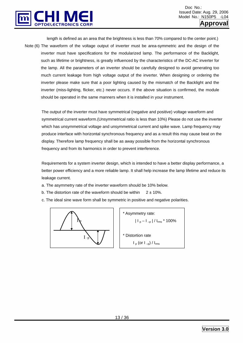
a. The asymmetry rate of the inverter waveform should be 10% below.
b. The distortion rate of the waveform should be within √2 ± 10%.
c. The ideal sine wave form shall be symmetric in positive and negative polarities.
I p
I -p
* Asymmetry rate:
| I p – I –p | / Irms * 100%
* Distortion rate
I p (or I –p) / Irms
Doc No.: Issued Date: Aug. 29, 2006
Model No.: N150P5 -L04
Approval
14 / 36 Version 3.0
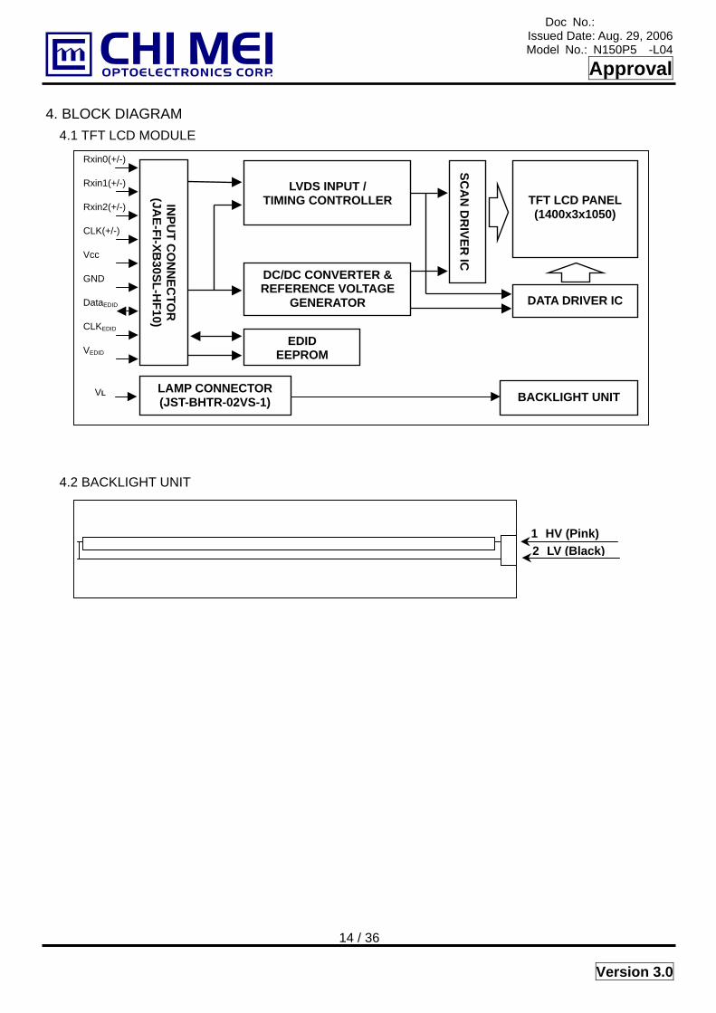
4. BLOCK DIAGRAM 4.1 TFT LCD MODULE
4.2 BACKLIGHT UNIT
VEDID
DataEDID
Vcc
1 HV (Pink) 2 LV (Black)
GND
VL
CLK(+/-)
Rxin2(+/-)
Rxin1(+/-)
Rxin0(+/-)
TFT LCD PANEL(1400x3x1050)
DATA DRIVER IC
SCA
N D
RIVER
IC
BACKLIGHT UNIT
LVDS INPUT /
TIMING CONTROLLER
DC/DC CONVERTER &REFERENCE VOLTAGE
GENERATOR
INPU
T CO
NN
ECTO
R
(JAE-FI-XB
30SL-HF10)
LAMP CONNECTOR (JST-BHTR-02VS-1)
EDID EEPROM
CLKEDID

Doc No.: Issued Date: Aug. 29, 2006
Model No.: N150P5 -L04
Approval
15 / 36 Version 3.0
5. INPUT TERMINAL PIN ASSIGNMENT 5.1 TFT LCD MODULE
Pin Symbol Description Polarity Remark 1 Vss Ground - 2 Vcc Power Supply +3.3 V - 3 Vcc Power Supply +3.3 V - 4 VEDID DDC +3.3V - 5 NC Non-Connection - 6 CLKEDID DDC Clock - 7 DATAEDID DDC Data - 8 RXO0- LVDS Differential Data Input (Odd) Negative 9 RXO0+ LVDS Differential Data Input (Odd) Positive R0~R5,G0
10 Vss Ground - 11 RXO1- LVDS Differential Data Input (Odd) Negative 12 RXO1+ LVDS Differential Data Input (Odd) Positive G1~G5,B0,B1
13 Vss Ground - 14 RXO2- LVDS Differential Data Input (Odd) Negative 15 RXO2+ LVDS Differential Data Input (Odd) Positive B2~B5,DE,Hsync,Vsync
16 Vss Ground - 17 RXOC- LVDS Clock Data Input (Odd) Negative 18 RXOC+ LVDS Clock Data Input (Odd) Positive LVDS Level
19 Vss Ground - 20 RxE0- LVDS Differential Data Input (Even) Negative 21 RxE0+ LVDS Differential Data Input (Even) Positive R0~R5,G0
22 Vss Ground - 23 RxE1- LVDS Differential Data Input (Even) Negative 24 RxE1+ LVDS Differential Data Input (Even) Positive G1~G5,B0,B1
25 Vss Ground - 26 RxE2- LVDS Differential Data Input (Even) Negative 27 RxE2+ LVDS Differential Data Input (Even) Positive B2~B5,DE,Hsync,Vsync
28 Vss Ground - 29 RXEC- LVDS Clock Data Input (Even) Negative 30 RXEC+ LVDS Clock Data Input (Even) Positive LVDS Level
Note (1) Connector Part No.: JAE-FI-XB30SRL-HF11
Note (2) User’s connector Part No: JAE-FI-X30C2L
Note (3) The first pixel is odd as shown in the following figure.
Doc No.: Issued Date: Aug. 29, 2006
Model No.: N150P5 -L04
Approval
16 / 36 Version 3.0
5.2 BACKLIGHT UNIT Pin Symbol Description Color 1 HV High Voltage Pink 2 LV Ground Black
Note (1) Connector Part No.: JST-BHTR-02VS-1 or equivalent
Note (2) User’s connector Part No.: JST-SM02B-BHTS-B-TB or equivalent

Doc No.: Issued Date: Aug. 29, 2006
Model No.: N150P5 -L04
Approval
17 / 36 Version 3.0
5.3 TIMING DIAGRAM OF LVDS INPUT SIGNAL
IN6 IN5 IN4 IN3 IN2 IN1 IN0
IN13 IN12 IN11 IN10 IN9 IN8 IN7
IN20 IN19 IN18 IN17 IN16 IN15 IN14
G0 R3 R2 R1 R0R5 R4
B1 G4 G3 G2 G1B0 G5
DE B5 B4 B3 B2Vsync Hsync
T/7
Signal for 1 DCLK Cycle (T)
RXE0+
RXE1+
RXE2+
RXEC+
IN6 IN5 IN4 IN3 IN2 IN1 IN0
IN13 IN12 IN11 IN10 IN9 IN8 IN7
IN20 IN19 IN18 IN17 IN16 IN15 IN14
G0 R3 R2 R1 R0R5 R4
B1 G4 G3 G2 G1B0 G5
DE B5 B4 B3 B2Vsync Hsync
T/7
Signal for 1 DCLK Cycle (T)
RXO0+
RXO1+
RXO2+
RXOC+

Doc No.: Issued Date: Aug. 29, 2006
Model No.: N150P5 -L04
Approval
18 / 36 Version 3.0
5.4 COLOR DATA INPUT ASSIGNMENT The brightness of each primary color (red, green and blue) is based on the 6-bit gray scale data input for
the color. The higher the binary input the brighter the color. The table below provides the assignment of
color versus data input. Data Signal
Red Green Blue Color R5 R4 R3 R2 R1 R0 G5 G4 G3 G2 G1 G0 B5 B4 B3 B2 B1 B0
Basic Colors
Black Red Green Blue Cyan Magenta Yellow White
01000111
0 1 0 0 0 1 1 1
0 1 0 0 0 1 1 1
0 1 0 0 0 1 1 1
01000111
01000111
00101011
00101011
00101011
00101011
00101011
00101011
0 0 0 1 1 1 0 1
0 0 0 1 1 1 0 1
0 0 0 1 1 1 0 1
0 0 0 1 1 1 0 1
00011101
00011101
Gray Scale Of Red
Red(0)/Dark Red(1) Red(2)
: :
Red(61) Red(62) Red(63)
000::111
0 0 0 : : 1 1 1
0 0 0 : : 1 1 1
0 0 0 : : 1 1 1
001::011
010::101
000::000
000::000
000::000
000::000
000::000
000::000
0 0 0 : : 0 0 0
0 0 0 : : 0 0 0
0 0 0 : : 0 0 0
0 0 0 : : 0 0 0
000::000
000::000
Gray Scale Of Green
Green(0)/Dark Green(1) Green(2)
: :
Green(61) Green(62) Green(63)
000::000
0 0 0 : : 0 0 0
0 0 0 : : 0 0 0
0 0 0 : : 0 0 0
000::000
000::000
000::111
000::111
000::111
000::111
001::011
010::101
0 0 0 : : 0 0 0
0 0 0 : : 0 0 0
0 0 0 : : 0 0 0
0 0 0 : : 0 0 0
000::000
000::000
Gray Scale Of Blue
Blue(0)/Dark Blue(1) Blue(2)
: :
Blue(61) Blue(62) Blue(63)
000::000
0 0 0 : : 0 0 0
0 0 0 : : 0 0 0
0 0 0 : : 0 0 0
000::000
000::000
000::000
000::000
000::000
000::000
000::000
000::000
0 0 0 : : 1 1 1
0 0 0 : : 1 1 1
0 0 0 : : 1 1 1
0 0 0 : : 1 1 1
001::011
010::101
Note (1) 0: Low Level Voltage, 1: High Level Voltage

Doc No.: Issued Date: Aug. 29, 2006
Model No.: N150P5 -L04
Approval
19 / 36 Version 3.0
5.5 EDID DATA STRUCTURE The EDID (Extended Display Identification Data) data formats are to support displays as defined in the
VESA Plug & Display and FPDI standards. Byte #
(decimal) Byte # (hex) Field Name and Comments Value
(hex) Value
(binary)0 0 Header 00 000000001 1 Header FF 111111112 2 Header FF 111111113 3 Header FF 111111114 4 Header FF 111111115 5 Header FF 111111116 6 Header FF 111111117 7 Header 00 000000008 8 EISA ID manufacturer name (“CMO”) 0D 000011019 9 EISA ID manufacturer name (Compressed ASCII) AF 10101111
10 0A ID product code 44 0100010011 0B ID product code 15 0001010112 0C ID S/N (fixed “0”) 00 0000000013 0D ID S/N (fixed “0”) 00 0000000014 0E ID S/N (fixed “0”) 00 0000000015 0F ID S/N (fixed “0”) 00 0000000016 10 Week of manufacture (fixed week code) 23 0010001117 11 Year of manufacture (fixed year code) 10 0001000018 12 EDID structure version # (“1”) 01 0000000119 13 EDID revision # (“3”) 03 0000001120 14 Video I/P definition (“digital”) 80 1000000021 15 Max H image size (“30.45 cm”) 1E 0001111022 16 Max V image size (“22.837 cm”) 17 0001011123 17 Display Gamma (Gamma = ”2.2”) 78 0111100024 18 Feature support (“Active off, RGB Color”) 0A 0000101025 19 Red/Green (Rx1, Rx0, Ry1, Ry0, Gx1, Gx0, Gy1, Gy0) 0A 0000101026 1A Blue/White (Bx1, Bx0, By1, By0, Wx1, Wx0, Wy1, Wy0) B5 1011010127 1B Red-x (Rx = “0.590”) 97 1001011128 1C Red-y (Ry = “0.340”) 57 0101011129 1D Green-x (Gx = ”0.318”) 51 0101000130 1E Green-y (Gy = ”0.537”) 89 1000100131 1F Blue-x (Bx = ”0.150”) 26 0010011032 20 Blue-y (By = ”0.120”) 1E 0001111033 21 White-x (Wx = ”0.313”) 50 0101000034 22 White-y (Wy = ”0.329”) 54 0101010035 23 Established timings 1 00 0000000036 24 Established timings 2 00 0000000037 25 Manufacturer’s reserved timings 00 0000000038 26 Standard timing ID # 1 01 0000000139 27 Standard timing ID # 1 01 0000000140 28 Standard timing ID # 2 01 0000000141 29 Standard timing ID # 2 01 00000001

Doc No.: Issued Date: Aug. 29, 2006
Model No.: N150P5 -L04
Approval
20 / 36 Version 3.0
Byte # (decimal)
Byte # (hex) Field Name and Comments Value
(hex) Value
(binary)42 2A Standard timing ID # 3 01 0000000143 2B Standard timing ID # 3 01 0000000144 2C Standard timing ID # 4 01 0000000145 2D Standard timing ID # 4 01 0000000146 2E Standard timing ID # 5 01 0000000147 2F Standard timing ID # 5 01 0000000148 30 Standard timing ID # 6 01 0000000149 31 Standard timing ID # 6 01 0000000150 32 Standard timing ID # 7 01 0000000151 33 Standard timing ID # 7 01 0000000152 34 Standard timing ID # 8 01 0000000153 35 Standard timing ID # 8 01 0000000154 36 Detailed timing description # 1 Pixel clock (“108 MHz”) 30 0011000055 37 # 1 Pixel clock (hex LSB first) 2A 0010101056 38 # 1 H active (“1400”) 78 0111100057 39 # 1 H blank (“288”) 20 0010000058 3A # 1 H active : H blank (“1400 : 288”) 51 0101000159 3B # 1 V active (”1050”) 1A 0001101060 3C # 1 V blank (”16”) 10 0001000061 3D # 1 V active : V blank (”1050 : 16”) 40 0100000062 3E # 1 H sync offset (”48”) 30 0011000063 3F # 1 H sync pulse width (”112”) 70 0111000064 40 # 1 V sync offset : V sync pulse width (”3 : 4”) 34 00110100
65 41 # 1 H sync offset : H sync pulse width : V sync offset : V sync width (”48 : 112 : 3 : 4”) 00 00000000
66 42 # 1 H image size (”304.5 mm”) 30 0011000067 43 # 1 V image size (”228.37 mm”) E4 1110010068 44 # 1 H image size : V image size (”304 : 228”) 10 0001000069 45 # 1 H boarder (”0”) 00 0000000070 46 # 1 V boarder (”0”) 00 00000000
71 47 # 1 Non-interlaced, Normal, no stereo, Separate sync, H/V pol Negatives 18 00011000
72 48 Detailed timing description # 2 00 0000000073 49 # 2 Flag 00 0000000074 4A # 2 Reserved 00 0000000075 4B # 2 FE (hex) defines ASCII string (Model Name “N150P5-L04”, ASCII) FE 1111111076 4C # 2 Flag 00 0000000077 4D # 2 1st character of name (“N”) 4E 0100111078 4E # 2 2nd character of name (“1”) 31 0011000179 4F # 2 3rd character of name (“5”) 35 0011010180 50 # 2 4th character of name (“0”) 30 0011000081 51 # 2 5th character of name (“P”) 50 0101000082 52 # 2 6th character of name (“5”) 35 0011010183 53 # 2 7th character of name (“-”) 2D 0010110184 54 # 2 8th character of name (“L”) 4C 01001100

Doc No.: Issued Date: Aug. 29, 2006
Model No.: N150P5 -L04
Approval
21 / 36 Version 3.0
Byte #
(decimal) Byte # (hex) Field Name and Comments Value
(hex) Value
(binary)85 55 # 2 9th character of name (“0”) 30 0011000086 56 # 2 10th character of name (“4”) 34 0011010087 57 (If <13 char, then terminate with ASCII code 0Ah, set remaining char = 20h) 0A 0000101088 58 (If <13 char, then terminate with ASCII code 0Ah, set remaining char = 20h) 20 0010000089 59 (If <13 char, then terminate with ASCII code 0Ah, set remaining char = 20h) 20 0010000090 5A Detailed timing description # 3 00 0000000091 5B # 3 Flag 00 0000000092 5C # 3 Reserved 00 0000000093 5D # 3 FE (hex) defines ASCII string (Vendor “CMO”, ASCII) FE 1111111094 5E # 3 Flag 00 0000000095 5F # 3 1st character of string (“C”) 43 0100001196 60 # 3 2nd character of string (“M”) 4D 0100110197 61 # 3 3rd character of string (“O”) 4F 0100111198 62 (If <13 char, then terminate with ASCII code 0Ah, set remaining char = 20h) 0A 0000101099 63 (If <13 char, then terminate with ASCII code 0Ah, set remaining char = 20h) 20 00100000100 64 (If <13 char, then terminate with ASCII code 0Ah, set remaining char = 20h) 20 00100000101 65 (If <13 char, then terminate with ASCII code 0Ah, set remaining char = 20h) 20 00100000102 66 (If <13 char, then terminate with ASCII code 0Ah, set remaining char = 20h) 20 00100000103 67 (If <13 char, then terminate with ASCII code 0Ah, set remaining char = 20h) 20 00100000104 68 (If <13 char, then terminate with ASCII code 0Ah, set remaining char = 20h) 20 00100000105 69 (If <13 char, then terminate with ASCII code 0Ah, set remaining char = 20h) 20 00100000106 6A (If <13 char, then terminate with ASCII code 0Ah, set remaining char = 20h) 20 00100000107 6B (If <13 char, then terminate with ASCII code 0Ah, set remaining char = 20h) 20 00100000108 0A Detailed timing description # 4 00 00000000109 6D # 4 Flag 00 00000000110 6E # 4 Reserved 00 00000000111 6F # 4 FE (hex) defines ASCII string (Model Name“N150P5-L04”, ASCII) FE 11111110112 70 # 4 Flag 00 00000000113 71 # 4 1st character of name (“N”) 4E 01001110114 72 # 4 2nd character of name (“1”) 31 00110001115 73 # 4 3rd character of name (“5”) 35 00110101116 74 # 4 4th character of name (“0”) 30 00110000117 75 # 4 5th character of name (“P”) 50 01010000118 76 # 4 6th character of name (“5”) 35 00110101119 77 # 4 7th character of name (“-”) 2D 00101101120 78 # 4 8th character of name (“L”) 4C 01001100121 79 # 4 9th character of name (“0”) 30 00110000122 7A # 4 10th character of name (“4”) 34 00110100123 7B (If <13 char, then terminate with ASCII code 0Ah, set remaining char = 20h) 0A 00001010124 7C (If <13 char, then terminate with ASCII code 0Ah, set remaining char = 20h) 20 00100000125 7D (If <13 char, then terminate with ASCII code 0Ah, set remaining char = 20h) 20 00100000126 7E Extension flag 00 00000000127 7F Checksum 24 00100100

Doc No.: Issued Date: Aug. 29, 2006
Model No.: N150P5 -L04
Approval
22 / 36 Version 3.0
6. INTERFACE TIMING 6.1 INPUT SIGNAL TIMING SPECIFICATIONS
The input signal timing specifications are shown as the following table and timing diagram. Signal Item Symbol Min. Typ. Max. Unit Note
DCLK Frequency 1/Tc 51 54 57 MHz - Vertical Total Time TV 1058 1066 2046 TH -
Vertical Addressing Time TVD 1050 1050 1050 TH - Horizontal Total Time TH 762 844 1023 Tc - DE
Horizontal Addressing Time THD 700 700 700 Tc -
INPUT SIGNAL TIMING DIAGRAM
6.2 POWER ON/OFF SEQUENCE
TH
TC DCLK
THD
TVD
Tv
DE
DE
DATA
- Power Supply for LCD, Vcc
- Interface Signal (LVDS Signal of Transmitter), VI
- Power for Lamp
Restart Power On Power Off
0V
0V 10%
t6 t5
t4
t3t2
t1 10%
90%
10%
90%
Valid Data
ONOFF OFF

Doc No.: Issued Date: Aug. 29, 2006
Model No.: N150P5 -L04
Approval
23 / 36 Version 3.0
Timing Specifications:
0 ≦ t1 ≦ 10 msec
0 < t2 ≦ 50 msec
0 < t3 ≦ 50 msec
t4 ≧ 200 msec
t5 ≧ 200 msec
t6 ≧ 120 msec
Note (1) Please avoid floating state of interface signal at invalid period.
Note (2) When the interface signal is invalid, be sure to pull down the power supply of LCD Vcc to 0 V.
Note (3) The Backlight inverter power must be turned on after the power supply for the logic and the
interface signal is valid. The Backlight inverter power must be turned off before the power supply
for the logic and the interface signal is invalid.
Note (4) Sometimes some slight noise shows when LCD is turned off (even backlight is already off). To
avoid this phenomenon, we suggest that the Vcc falling time had better to follow t7 ≧ 5 msec
6.3 VCC DIP CONDITIONS
(1) 2.5V≦ VCC< 3.0V
Td≦20 ms
(2) VCC< 2.5V
Vcc-Dip conditions also follow the power up/down conditions for supply voltage.
GND
3.0 V2.5V
VCC
Td
Doc No.: Issued Date: Aug. 29, 2006
Model No.: N150P5 -L04
Approval
24 / 36 Version 3.0
7. OPTICAL CHARACTERISTICS 7.1 TEST CONDITIONS
Item Symbol Value Unit Ambient Temperature Ta 25±2 oC Ambient Humidity Ha 50±10 %RH Supply Voltage VCC 3.3 V Input Signal According to typical value in "3. ELECTRICAL CHARACTERISTICS" Inverter Current IL 6.0 mA Inverter Driving Frequency FL 61 KHz Inverter Sumida H05-4915 The measurement methods of optical characteristics are shown in Section 7.2. The following items should be measured under the test conditions described in Section 7.1 and stable environment shown in Note (6).
7.2 OPTICAL SPECIFICATIONS Item Symbol Condition Min. Typ. Max. Unit Note
Contrast Ratio CR 300 400 - - (2), (6)TR - 5 10 ms Response Time TF - 11 16 ms (3)
Average Luminance of White ( 5 points ) LAVE 170 200 - cd/m2 (4), (6)Cross Modulation Dsha -- -- 2 % (5), (6)13 Points White Variation δW -- -- 2 -- (6), (7)13 Points CR Variation CVER -- -- 2.0 -- (6), (7)
White Variation dL -- -- 1.5 %/mm (6), (8)Rx 0.590 -- Red Ry 0.340 -- Gx 0.318 -- Green Gy 0.537 -- Bx 0.150 -- Blue By 0.120 -- Wx 0.313 --
Color Chromaticity
White Wy
θx=0°, θY =0° Viewing Normal
Angle
TYP-0.03
0.329
TYP +0.03
-- θx+ 40 45 - Horizontal θx- 40 45 - θY+ 15 20 -
Viewing Angle Vertical
θY-
CR≥10
40 45 -
Deg.
θx+ 50 60 -- Horizontal θx- 50 60 -- θY+ 20 30 --
Viewing Angle Vertical
θY-
CR≥5
45 55 --
Deg.
(1), (6)
Specifications Item Symbol Conditions
Min. Typ. Max.Unit Note
63 100 100 100 60 83.4 89.8 96.9
Gamma
56
θX = θY =0°
Viewing normal angle 65.6 77.2 91.3
% 8. (6) at center of
Viewing area
Doc No.: Issued Date: Aug. 29, 2006
Model No.: N150P5 -L04
Approval
25 / 36 Version 3.0
52 51.7 65.6 83.6 48 40.4 55.0 74.8 44 32.1 45.4 66.4 40 25.0 36.8 57.5 36 19.1 29.2 48.4 32 14.2 22.5 39.4 28 10.5 16.8 31.4 24 7.4 12.0 23.6 20 4.8 8.0 16.4 16 2.8 4.9 10.1 12 1.4 2.6 5.3 8 0.5 1.1 2.5 4 0.1 0.2 0.8
0
0 0 0
center only

Doc No.: Issued Date: Aug. 29, 2006
Model No.: N150P5 -L04
Approval
26 / 36 Version 3.0
Note (1) Definition of Viewing Angle (θx, θy):
Note (2) Definition of Contrast Ratio (CR):
The contrast ratio can be calculated by the following expression.
Contrast Ratio (CR) = L63 / L0
L63: Luminance of gray level 63
L 0: Luminance of gray level 0
CR = CR (1)
CR (X) is corresponding to the Contrast Ratio of the point X at Figure in Note (7).
Note (3) Definition of Response Time (TR, TF):
12 o’clock direction
θy+ = 90º
6 o’clock
θy- = 90º
θx− θx+
θy- θy+
x- y+
y- x+
Normal
θx = θy = 0º
θX+ = 90º
θX- = 90º
100%
90%
10%
0%
Gray Level 63
Gray Level 0
Gray Level 63
Time TF
Optical
Response
TR
66.67 ms 66.67 ms
Doc No.: Issued Date: Aug. 29, 2006
Model No.: N150P5 -L04
Approval
27 / 36 Version 3.0
Note (4) Definition of Average Luminance of White (LAVE):
Measure the luminance of gray level 63 at 5 points
LAVE = [L (1)+ L (2)+ L (3)+ L (4)+ L (5)] / 5
L (x) is corresponding to the luminance of the point X at Figure in Note (7)
Note (5) Definition of Cross Modulation (DSHA)
DSHA = | YB – YA | / YA ×100 (%) Where:
YA = Luminance of measured location without gray level 0 pattern (cd/m2)
YB = Luminance of measured location with gray level 0 pattern (cd/m2)
Note (6) Measurement Setup:
The LCD module should be stabilized at given temperature for 15 minutes to avoid abrupt temperature
change during measuring. In order to stabilize the luminance, the measurement should be executed
after lighting Backlight for 15 minutes in a windless room.
Active Area YA, U (D/2,W/8)
YA, R (7D/8,W/2)
YA, D (D/2,7W/8)
YA, L (D/8,W/2)
(0, 0)
(D,W)
Gray 128
Active Area
Gray 0
(D/4,W/4)
(3D/4,3W/4)
(0, 0)YB, U (D/2,W/8)
YB, R (7D/8,W/2)
YB, D (D/2,7W/8)
YB, L (D/8,W/2)
(D,W)Gray 128
TOPCON/BM-5A
MINOLTA /CA210
MINOLTA /CS-1000T
Field of View = 2º
500 mm
LCD Module
LCD Panel
Center of the Screen
Light Shield Room
(Ambient Luminance < 2 lux)
Doc No.: Issued Date: Aug. 29, 2006
Model No.: N150P5 -L04
Approval
28 / 36 Version 3.0
Note (7) Definition of White Variation (δW):
Measure the luminance of gray level 63 at 13 points
δW = Maximum [L (1) ~ L (13)] / Minimum [L (1) ~ L (13)]
CVER = Maximum [CR (1) ~ CR (13)] / Minimum [CR (1) ~ CR (13)]
Note (8) Definition of Luminance Variation (dL):
Measure the luminance of gray level 63 along the 5 lines in Horizontal and Vertical direction which is described in below picture. The distance between measured point to next point is 5mm.
dL = | Bm-1 – Bm | /{5 × ( B1 + B2 ⋯ Bn-1 + Bn )/n}×100 % Where:
Bx = Luminance of measured location x , x =1~n
2 ≦ m ≦ n where n ,m is an integer.
The distance between Bm-1 and Bm is 5mm
6 7 8
2 3
1
4 5
11 12 13
9 10
W
H
10mm 10mm
W/4 W/4 W/4 W/4
H/4
10mm
H/4
H/4
H/4
10mm
:Test Point X=1 to 13
X
Horizontal Line Number
Verti
cal L
ine
Num
ber
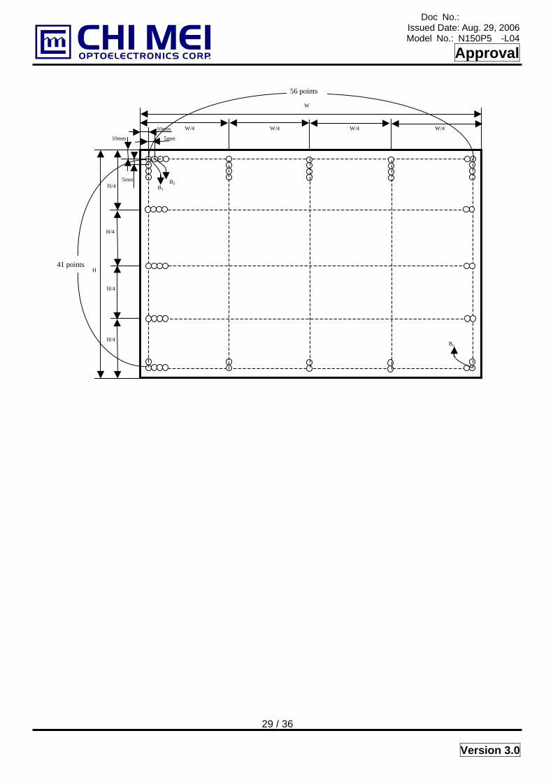
Doc No.: Issued Date: Aug. 29, 2006
Model No.: N150P5 -L04
Approval
29 / 36 Version 3.0
10mm
5mm
10mm
5mm
W
H
H/4
H/4
H/4
H/4
W/4 W/4 W/4 W/4
56 points
41 points
B1 B2
Bn
Doc No.: Issued Date: Aug. 29, 2006
Model No.: N150P5 -L04
Approval
30 / 36 Version 3.0
8. PRECAUTIONS 8.1 HANDLING PRECAUTIONS
(1) The module should be assembled into the system firmly by using every mounting hole. Be careful not
to twist or bend the module.
(2) While assembling or installing modules, it can only be in the clean area. The dust and oil may cause
electrical short or damage the polarizer.
(3) Use fingerstalls or soft gloves in order to keep display clean during the incoming inspection and
assembly process.
(4) Do not press or scratch the surface harder than a HB pencil lead on the panel because the polarizer is
very soft and easily scratched.
(5) If the surface of the polarizer is dirty, please clean it by some absorbent cotton or soft cloth. Do not use
Ketone type materials (ex. Acetone), Ethyl alcohol, Toluene, Ethyl acid or Methyl chloride. It might
permanently damage the polarizer due to chemical reaction.
(6) Wipe off water droplets or oil immediately. Staining and discoloration may occur if they left on panel for
a long time.
(7) If the liquid crystal material leaks from the panel, it should be kept away from the eyes or mouth. In
case of contacting with hands, legs or clothes, it must be washed away thoroughly with soap.
(8) Protect the module from static electricity, it may cause damage to the C-MOS Gate Array IC.
(9) Do not disassemble the module.
(10) Do not pull or fold the lamp wire.
(11) Pins of I/F connector should not be touched directly with bare hands.
8.2 STORAGE PRECAUTIONS
(1) High temperature or humidity may reduce the performance of module. Please store LCD module within
the specified storage conditions.
(2) It is dangerous that moisture come into or contacted the LCD module, because the moisture may
damage LCD module when it is operating.
(3) It may reduce the display quality if the ambient temperature is lower than 10 ºC. For example, the
response time will become slowly, and the starting voltage of lamp will be higher than the room
temperature.
8.3 OPERATION PRECAUTIONS (1) Do not pull the I/F connector in or out while the module is operating.
(2) Always follow the correct power on/off sequence when LCD module is connecting and operating. This
can prevent the CMOS LSI chips from damage during latch-up.
(3) The startup voltage of Backlight is approximately 1000 Volts. It may cause electrical shock while
assembling with inverter. Do not disassemble the module or insert anything into the Backlight unit.

Doc No.: Issued Date: Aug. 29, 2006
Model No.: N150P5 -L04
Approval
31 / 36 Version 3.0
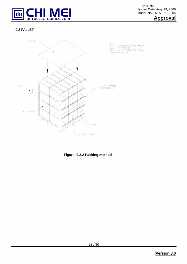
9. PACKING 9.1 PACKING SPECIFICATIONS
(1) 20 LCD modules / 1 Box
(2) Box dimensions: 500(L) X 600(W) X 362(H) mm
(3) Weight: approximately 13 Kg (20 modules per box)
9.2 PACKING METHOD
(1)Carton Packing should have no failure in the following reliability test items.
Test Item Test Conditions Note
Vibration Frequency Range: 2 – 200 Hz, Random, +X: 10min,+Y: 10min,+Z: 10min,-Z: 30 min follow ISTA standard. Non Operation
Dropping Test 1 Angle, 3 Edge, 6 Face, 60cm Non Operation 9.2.1 CARTON
Figure. 9.2.1 Packing method
Doc No.: Issued Date: Aug. 29, 2006
Model No.: N150P5 -L04
Approval
32 / 36 Version 3.0
9.2 PALLET
Figure. 9.2.2 Packing method
Doc No.: Issued Date: Aug. 29, 2006
Model No.: N150P5 -L04
Approval
33 / 36 Version 3.0
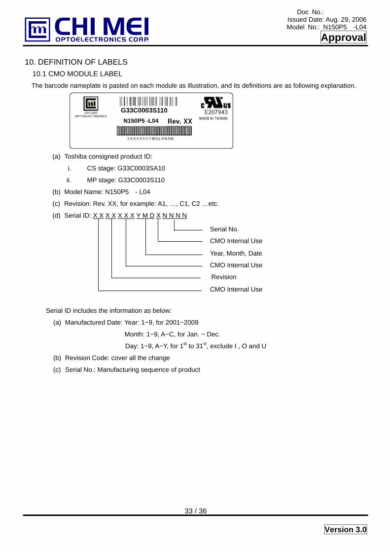
10. DEFINITION OF LABELS
10.1 CMO MODULE LABEL The barcode nameplate is pasted on each module as illustration, and its definitions are as following explanation.
(a) Toshiba consigned product ID:
i. CS stage: G33C0003SA10
ii. MP stage: G33C0003S110
(b) Model Name: N150P5 - L04
(c) Revision: Rev. XX, for example: A1, …, C1, C2 …etc.
(d) Serial ID: X X X X X X X Y M D X N N N N
Serial ID includes the information as below:
(a) Manufactured Date: Year: 1~9, for 2001~2009
Month: 1~9, A~C, for Jan. ~ Dec.
Day: 1~9, A~Y, for 1st to 31st, exclude I , O and U
(b) Revision Code: cover all the change
(c) Serial No.: Manufacturing sequence of product
Year, Month, Date CMO Internal Use Revision
Serial No.
CMO Internal Use
CMO Internal Use
N150P5 -L04
G33C0003S110
Doc No.: Issued Date: Aug. 29, 2006
Model No.: N150P5 -L04
Approval
34 / 36 Version 3.0
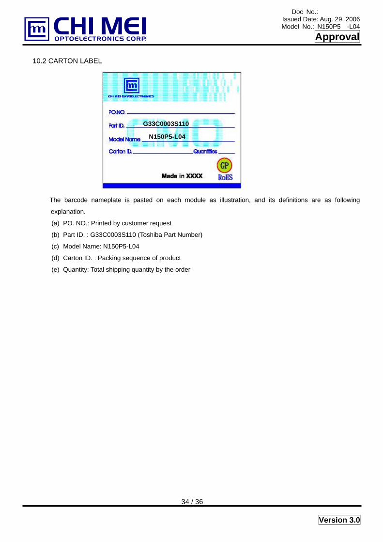
10.2 CARTON LABEL
The barcode nameplate is pasted on each module as illustration, and its definitions are as following
explanation.
(a) PO. NO.: Printed by customer request
(b) Part ID. : G33C0003S110 (Toshiba Part Number)
(c) Model Name: N150P5-L04
(d) Carton ID. : Packing sequence of product
(e) Quantity: Total shipping quantity by the order
N150P5-L04
G33C0003S110
Related Documents


