www.renesa s.com All information contained in these materials, including products and product specifications, represents information on the product at the time of publication and is subject to change by Renesas Electronics Corp. without notice. Please review the latest information published by Renesas Electronics Corp. through various means, including the Renesas Technology Corp. website (http://www.renesas.com). The newest version of this document can be obtained from the following web location http://www.renesas.eu/updates?oc=Y-RH850-F1X-176PIN-PB-T1-V4 RH850 Evaluation Platform RH850/F1x-176pin PiggyBack board Y-RH850-F1X-176PIN-PB-T1-V4 R20UT4148ED0110, Rev. 1.10 2017-08-22 Use r´s Manual 32

Welcome message from author
This document is posted to help you gain knowledge. Please leave a comment to let me know what you think about it! Share it to your friends and learn new things together.
Transcript

www.renesa s.com
All information contained in these materials, including products and product specifications,
represents information on the product at the time of publication and is subject to change by
Renesas Electronics Corp. without notice. Please review the latest information published by
Renesas Electronics Corp. through various means, including the Renesas Technology Corp.
website (http://www.renesas.com).
The newest version of this document can be obtained from the following web location
http://www.renesas.eu/updates?oc=Y-RH850-F1X-176PIN-PB-T1-V4
RH850 Evaluation Platform
RH850/F1x-176pin PiggyBack board
Y-RH850-F1X-176PIN-PB-T1-V4
R20UT4148ED0110, Rev. 1.10 2017-08-22
U
ser´s
Manual
32


Table of Contents
Chapter 1 Introduction ......................................................................... 5
Chapter 2 Overview .............................................................................. 6
2.1 Overview ............................................................................................... 6
2.2 Mounting of the device ........................................................................ 7
Chapter 3 Jumper Configuration ......................................................... 8
Chapter 4 Power supply ..................................................................... 10
4.1 Board power connection ................................................................... 10
4.2 Voltage distribution ............................................................................ 11
Chapter 5 Clock sources .................................................................... 12
5.1 MainOsc .............................................................................................. 12
5.2 SubOSC ............................................................................................... 12
Chapter 6 Debug and Programming interface .................................. 13
Chapter 7 Connectors for ports of device ......................................... 14
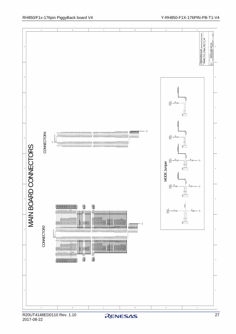
Chapter 8 Connectors to MainBoard ................................................. 15
8.1 Connector CN1 ................................................................................... 15
8.2 Connector CN2 ................................................................................... 17
8.3 Connector CN3 ................................................................................... 19
Chapter 9 Other circuitry .................................................................... 21
9.1 Push button for RESET ...................................................................... 21
9.2 Mode Selection ................................................................................... 21
9.3 Signalling LEDs .................................................................................. 22
Chapter 10 Mechanical dimensions .................................................... 23
Chapter 11 Schematic .......................................................................... 24
Chapter 12 Revision History ................................................................ 28

RH850/F1x-176pin PiggyBack board V4 Y-RH850-F1X-176PIN-PB-T1-V4
R20UT4148ED0110 Rev. 1.10 5 2017-08-22
Chapter 1 Introduction
The RH850/F1x Application Board is part of the RH850 Evaluation Platform and serves as a simple and easy to use platform for evaluating the features and performance of Renesas Electronics 32-bit RH850/F1x microcontrollers. The piggyback board (Y-RH850-F1X-176PIN-PB-T1-V4) can be used as a standalone board, or can be mated with a mainboard (e.g. Y-RH850-X1X-MB-Tx-Vx) for extended functionality.
Main features:
Socket for mounting of device
Standalone operation of the board
Direct supply of device voltage (typ. 3.3V-5.0V)
Device programming capability
Device debugging capability
Pin headers for direct access to each device pin
Reset switch
MainOSC and SubOSC circuitry
Signal LEDs
Jumpers for device mode selection
Connectors to MainBoard
This document describes the functionality provided by the piggyback board and guides the user through its operation.
For details regarding the operation of the microcontroller, refer to the related User’s Manual and Datasheet.
This manual describes the following board revision:
Y-RH850-F1X-176PIN-PB-T1-V4
The main difference to the previous board revision (Y-RH850-F1X-176PIN-PB-T1-V3) are:
Added support for the RH850/F1KH-D8 device. (Especially see the Note in chapter 4.2 for the configuration of the REGnVCC voltage.)
Modified port assignments on connectors to MainBoard (CN1 to CN3)

RH850/F1x-176pin PiggyBack board V4 Y-RH850-F1X-176PIN-PB-T1-V4
R20UT4148ED0110 Rev. 1.10 6 2017-08-22
Chapter 2 Overview
2.1 Overview
Figures 1 and 2 provide the views of the Piggyback Board.
Figure 1 – PiggyBoard top view
Figure 2 – PiggyBoard bottom view
Devic
e p
in #
1

RH850/F1x-176pin PiggyBack board V4 Y-RH850-F1X-176PIN-PB-T1-V4
R20UT4148ED0110 Rev. 1.10 7 2017-08-22
2.2 Mounting of the device
The board is designed for use with the following devices (each in the 176pin package version):
RH850/F1L
RH850/F1M
RH850/F1H
RH850/F1K
RH850/F1KM-S4
RH850/F1KH-D8
The device must be placed inside the socket IC1. To insert the device, press down the lid, align the #1 pin of the device to the #1pin of the socket, insert the device inside the socket and release the lid.

RH850/F1x-176pin PiggyBack board V4 Y-RH850-F1X-176PIN-PB-T1-V4
R20UT4148ED0110 Rev. 1.10 8 2017-08-22
Chapter 3 Jumper Configuration
The function of the board can be configured via jumpers. This chapter describes the standard configuration, i.e. jumper setting for the intended devices. For the supported function of the used device, please refer to the corresponding HW user’s manual.
The table has the following meaning:
x-y: Connect the pins x and y; valid for 3-pin jumpers (e.g. JP17)
The pin #1 can be identified by a small circle in the vicinity of the jumper
Depending on the used device a configuration of several jumpers is required. The detailed configuration is shown below:
F1L F1M F1H F1K F1KM-S4 F1KH-D8 Function
JP1 closed open open closed open open Selection of Pin 114: P9_6, VSS, REG0VCC or REG1VCC
JP2 open closed closed open open open
JP3 open open open open closed open
JP31 open open open open open closed
JP4 closed open open closed open open Selection of Pin 113: P9_5, REGVCC or VSS
JP5 open closed closed open open open
JP6 open open open open closed closed
JP7 1-2 closed closed closed closed open open Selection of Pin 73: P1_6 or ISOVCL JP7 2-3 open open open open closed closed
JP8 1-2 closed closed closed closed open open Selection of Pin 72: P1_7 or VSS JP8 2-3 open open open open closed closed
JP9 1-2 closed closed closed closed open open Selection of Pin 14: P11_14 or VSS JP9 2-3 open open open open closed closed
JP10 1-2 closed closed closed closed open open Selection of Pin 13: P11_13 or ISOVCL JP10 2-3 open open open open closed closed
JP21 1-2 closed open open Either open open Selection of PWGA34: Either from P9_5 or P0_11 JP21 2-3 open closed closed Or closed closed
JP17 1-2 closed open open Either open open Selection of PWGA35: Either P9_6 or P0_6 JP17 2-3 open closed closed Or closed closed
JP24 1-2 open open closed open open open Selection of ETH0RXERR: Either P11_14 or P11_15 JP24 2-3 open open open open closed closed
JP30 1-2 open open open open closed closed Selection of ETH0CRSDV: Either P11_12 or P11_13 JP30 2-3 open open closed open open open
JP36 1-2 Either Either Either Either Either Either Selection of UART0TX: Either P10_10 or P0_2 JP36 2-3 Or Or Or Or Or Or
JP37 1-2 Either Either Either Either Either Either Selection of UART0RX: Either P10_9 or P0_3 JP37 2-3 Or Or Or Or Or Or
JP34 1-2 Either Either Either Either Either Either Selection of LIN0TX: Either P10_10 or P0_2 JP34 2-3 Or Or Or Or Or Or
JP35 1-2 Either Either Either Either Either Either Selection of LIN0RX: Either P10_9 or P0_3 JP35 2-3 Or Or Or Or Or Or
JP32 1-2 Either Either Either Either Either Either Selection of CAN0TX: Either P10_1 or P0_0 JP32 2-3 Or Or Or Or Or Or
JP33 1-2 Either Either Either Either Either Either Selection of CAN0RX: Either P10_0 or P0_1 JP33 2-3 Or Or Or Or Or Or

RH850/F1x-176pin PiggyBack board V4 Y-RH850-F1X-176PIN-PB-T1-V4
R20UT4148ED0110 Rev. 1.10 9 2017-08-22
The jumper setting also are shown in this picture:
Figure 3 – Jumper setting overview
The green jumper JP25 for FLMDO0 always must be closed for a ‘normal’ (user mode and debug) operation of the device.
The red jumpers must be set for a single “Voltage 1” (typ +5.0V) operation of the device.
The blue jumper must be set for a single “Voltage 2” (typ +3.3V) operation of the device.
The orange jumpers must be selected depending on the used device. See the printing on the board or the table above for the applicable setting.
For jumper settings related to the device operation mode, refer to the chapter 9.2.

RH850/F1x-176pin PiggyBack board V4 Y-RH850-F1X-176PIN-PB-T1-V4
R20UT4148ED0110 Rev. 1.10 10 2017-08-22
Chapter 4 Power supply
4.1 Board power connection
For operation of the device, a supply voltage must be connected to the board. Though a single supply voltage is sufficient for the operation of the device, two (different) voltages can be supplied to the board.
Within this document the following voltages are considered as ‘typical’ connections:
Voltage1 = 5.0V
Voltage2 = 3.3V
The following connectors are available to supply those voltages:
Three 4mm ‘banana-type’ connectors: - Two red connectors for voltages Voltage1 (CN54) and Voltage2 (CN17). - A black connector for VSS connection (CN10). Note: The three connectors are supplied with the board but not assembled.
The E1/E2 emulator that is used for debug purposes and flash programming can also supply a single operating voltage (‘Dbg_Voltage’). The voltage is programmable via the E1/E2 GUI as 3.3 or 5.0V (typ). See the documentation of the E1/E2 and chapter 5 ‘Debug and Programming interface’ for details. Note: The E1 voltage is connected to Voltage1, what is typically 5V. Still, 3.3V can be provided by the E1.
In case the PiggyBoard is mounted on a MainBoard, the voltages Voltage1 and Voltage2 are supplied by the on-board regulators of the MainBoard.
NOTE: Do not supply any voltage directly to the PiggyBoard in case it is mounted on the MainBoard.
For each of the two voltages, ‘Voltage 1 ‘ and ‘Voltage 2’, a green LED (LED1 and LED2) is available to signal that the related voltage is available on the PiggyBoard.
RH850/F1x-176pin PiggyBack board V4 Y-RH850-F1X-176PIN-PB-T1-V4
R20UT4148ED0110 Rev. 1.10 11 2017-08-22
4.2 Voltage distribution
The table shows the required device power supply pins and their function:
Device supply
pin
Name on PiggyBoard
Function
REGVCC REG0VCC
REG0VDD Supply for the device internal regulators for the digital logic.
REG1VCC REG1VDD Supply for the device internal regulators for the digital logic.
EVCC EVDD Supply for ports.
BVCC BVDD Supply for ports.
A0VREF Supply for ports and analog functions of ADC0.
A1VREF Supply for ports and analog functions of ADC1.
VDDIOF IO supply voltage for components located on a connected mainboard.
For each of the above voltages, the voltage source can be selected from Voltage1 (typ. 5.0V) or Voltage2 (typ. 3.3V) by the jumpers JP12-JP16, JP18, JP29, respectively the jumpers JP11 and JP20.
REG0VCC
JP20
VOLTAGE1
VOLTAGE2
VDDIOF
EVCC
BVCC
A0VREF
A1VREF
JP11
JP12
JP13
JP14
JP15
JP16
JP18
REG1VCC
JP29
Note:
The RH850/F1KH-D8 device requires a supply voltage of 3.3V on its REG1VCC pin.
The RH850/F1KM-S4 device requires the same supply voltage to be set to REG0VCC and REG1VCC.
See the section ‘Electrical Characteristics’ in the device User’s Manual for further details.

RH850/F1x-176pin PiggyBack board V4 Y-RH850-F1X-176PIN-PB-T1-V4
R20UT4148ED0110 Rev. 1.10 12 2017-08-22
Chapter 5 Clock sources
Four external crystal oscillators for the device clock supply are provided with the board.
5.1 MainOsc
A crystal or ceramic resonator can be mounted on socket X1. The applicable frequency range can be found is the devices electrical specification.
A 8MHz, 16MHz and a 20MHz oscillator is supplied with the board.
5.2 SubOSC
An oscillator with a frequency of 32.768kHz is supplied with the board and can be soldered into the connector X2.
RH850/F1x-176pin PiggyBack board V4 Y-RH850-F1X-176PIN-PB-T1-V4
R20UT4148ED0110 Rev. 1.10 13 2017-08-22
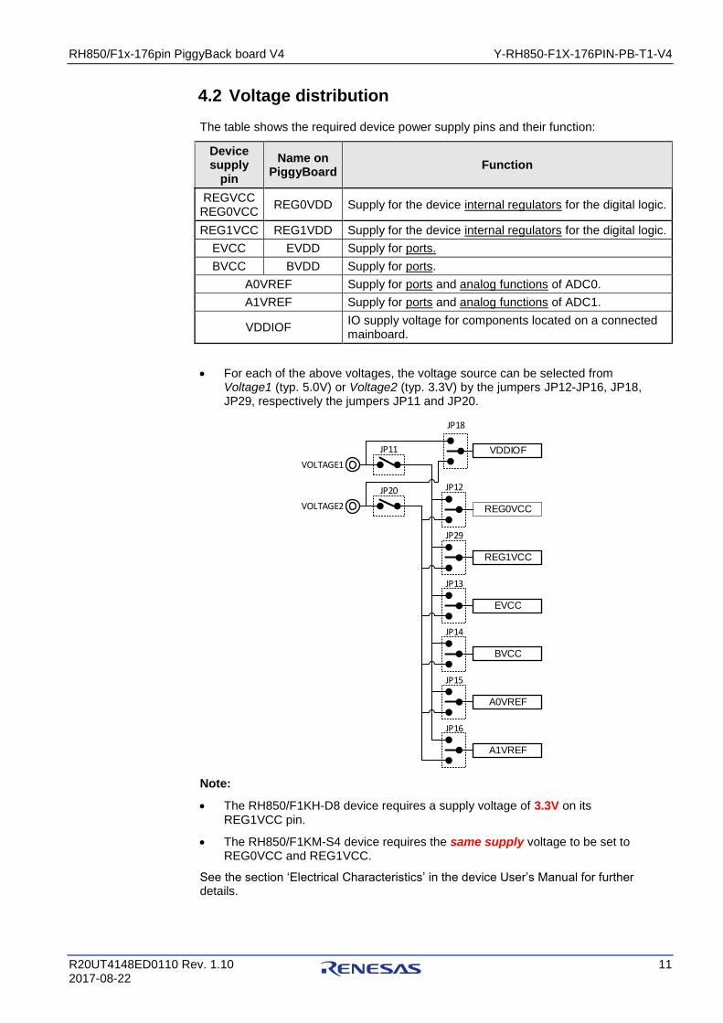
Chapter 6 Debug and Programming interface
For connection of the microcontroller debug and flash programming tools, the connector CN19 is provided.
The signal connection of the connector CN19 is shown in the picture below:
CN19 pin Device Port Device signal
1 JP0_2 DCUTCK / LPDCLK
2 GND GND
3 JP0_4 DCUTRST
4 FLMD0 FLMD0
5 JP0_1 DCUTDO / LPDO
6 P10_8* FLMD1
7 JP0_0 DCUTDI / LPDI
8 ‘Dbg_Voltage’ -
9 JP0_3 DCUTMS
10 JP0_6 EVTO*
11 JP0_5 DCURDY /
LPDCLKOUT
12 GND -
13 RESET -
14 GND -
*In case the EVTOUT signal shall be used by the debug/programming tool, the pin header JP11 must be closed.
The ‘Dbg_Voltage’ (on CN19 pin 8) is monitored or supplied by the debug and flash programming tools. Therefore, it is necessary to select either Voltage1 (5V) or the Voltage2 (3.3V) by pin header JP23:
JP23 pin Selection for Dbg_Voltage
1-2 5V is selected
2-3 3.3V is selected

RH850/F1x-176pin PiggyBack board V4 Y-RH850-F1X-176PIN-PB-T1-V4
R20UT4148ED0110 Rev. 1.10 14 2017-08-22
Chapter 7 Connectors for ports of device
Connection to each pin of the device is possible via the connectors CN5 to CN8.
Note: The pin headers are directly connected to the pins of the device, therefore special care must be taken to avoid any electrostatic or other damage to the device.

RH850/F1x-176pin PiggyBack board V4 Y-RH850-F1X-176PIN-PB-T1-V4
R20UT4148ED0110 Rev. 1.10 15 2017-08-22
Chapter 8 Connectors to MainBoard
Three connectors (CN1 to CN3) are available to connect the PiggyBoard to a MainBoard.
The function and port assignment of each connector pin is described in this chapter.
Note: Not each function may be available on the assigned device port for each of the supported devices of this PiggyBoard. In case a function is not available on the assigned device port but on a different port of the device, use one of the provided wires (with the MainBoard) for a manual connection of the device pin (via CN5 to CN8) to the related functional pin header on the MainBoard.
8.1 Connector CN1
Pin Function Device Port Pin Function Device Port
1 VOLTAGE1 - 2 VOLTAGE1 -
3 VOLTAGE1 - 4 VOLTAGE1 -
5 RESET _RESET 6 NMI P9_0
7 WAKE - 8 - -
9 INT0 P9_1 10 INT1 P0_6
11 INT2 P9_2 12 INT3 P9_3
13 - - 14 - -
15 UART0TX P10_10 or
P0_2 16 UART1TX P0_5
17 UART0RX P10_9 or
P0_3 18 UART1RX P0_4
19 LIN0TX P10_10 or
P0_2 20 LIN1TX P0_8
21 LIN0RX P10_9 or
P0_3 22 LIN1RX P0_7
23 IIC0SDL P10_3 24 IIC1SDL P9_1
25 IIC0SDA P10_2 26 IIC1SDA P9_0
27 CAN0TX P10_1 or
P0_0 28 CAN1TX P0_3
29 CAN0RX P10_0 or
P0_1 30 CAN1RX P0_2
31 SENTIN0 P8_0 32 SENTIN1 P9_0
33 SENTOUT0 P8_1 34 SENTOUT1 P9_1
35 PSI50Rx - 36 PSI51Rx -
37 PSI50Tx - 38 PSI51Tx -
39 PSI50Snyc - 40 PSI51Sync -
41 FLX0TX P11_1 42 FLX0EN P10_11
43 FLX0RX P10_14 44 FLXSTPWT P10_12
45 FLX1TX P10_8 46 FX1EN P10_13

RH850/F1x-176pin PiggyBack board V4 Y-RH850-F1X-176PIN-PB-T1-V4
R20UT4148ED0110 Rev. 1.10 16 2017-08-22
Pin Function Device Port Pin Function Device Port
47 FLX1RX P10_9 48 FX1CLK P10_10
49 - - 50 - -
51 ETH0MDIO P12_4 52 ETH0MDC P12_5
53 ETH0RXD0 P10_1 54 EH0TXD0 P18_1
55 ETH0RXD1 P10_2 56 EH0TXD1 P18_2
57 ETH0RXD2 P10_4 58 EH0TXD2 P18_3
59 ETH0RXD3 P10_5 60 EH0TXD3 P18_4
61 ETH0RXDCLK P10_0 62 ETH0TXCLK P18_7
63 ETH0RXER P11_14 or P11_15
64 ETH0TXER P18_6
65 ETH0CRSDV P11_12 or P11_13
66 ETH0TXEN P18_5
67 ETH0RXDV P11_11 68 ETH0COL P11_10
69 ETH0RESET P2_6 70 ETH0LINK P18_0
71 - - 72 - -
73 USB0UDMF - 74 USB0UDMH -
75 USB0UDPF - 76 USB0UDPH -
77 - - 78 - -
79 - - 80 - -
81 - - 82 - -
83 - - 84 - -
85 DIGIO_0 P8_0 86 DIGIO_1 P8_1
87 DIGIO_2 P8_2 88 DIGIO_3 P8_3
89 DIGIO_4 P8_4 90 DIGIO_5 P8_5
91 DIGIO_6 P8_6 92 DIGIO_7 P11_0
93 DIGIO_8 P10_0 94 DIGIO_9 P10_7
95 DIGIO_10 P10_8 96 DIGIO_11 P10_15
97 DIGIO_12 P0_9 98 DIGIO_13 P0_10
99 DIGIO_14 P0_11 100 DIGIO_15 P0_12
101 - - 102 - -
103 MUX0 P10_4 104 MUX1 P10_5
105 MUX2 P10_6 106 - -
107 ADC0 AP0_0 108 ADC1 AP0_1
109 ADC2 AP0_2 110 ADC3 AP0_3
111 ADC4 AP0_4 112 ADC5 AP0_5
113 ADC6 AP0_6 114 ADC7 AP0_7
115 VDDIOF - 116 VDDIOF -
117 VOLTAGE2 - 118 VOLTAGE2 -
119 VOLTAGE2 - 120 VOLTAGE2 -

RH850/F1x-176pin PiggyBack board V4 Y-RH850-F1X-176PIN-PB-T1-V4
R20UT4148ED0110 Rev. 1.10 17 2017-08-22
8.2 Connector CN2
Pin Function Device Port Pin Function Device Port
1 CAN2Tx P0_4 2 CAN3Tx P1_3
3 CAN2Rx P0_5 4 CAN3Rx P1_2
5 CAN4Tx P1_13 6 CAN5Tx P0_14
7 CAN4Rx P1_12 8 CAN5Rx P0_13
9 LIN2Tx P0_10 10 LIN3Tx P1_15
11 LIN2Rx P0_9 12 LIN3Rx P1_14
13 LIN4Tx P1_11 14 LIN5Tx P8_12
15 LIN4Rx P1_10 16 LIN5Rx P8_11
17 LIN6Tx P0_12 18 LIN7Tx P12_4
19
LIN6Rx P0_11 20 LIN7Rx P12_3
21 LIN8Tx P2_3 22 LIN9Tx P2_5
23 LIN8Rx P2_2 24 LIN9Rx P2_4
25 LIN10Tx P8_2 26 LIN11Tx P10_12
27 LIN10Rx P8_10 28 LIN11Rx P10_11
29 LIN12Tx P10_14 30 LIN13Tx P1_1
31 LIN12Rx P10_13 32 LIN13Rx P1_0
33 LIN14Tx P8_9 34 LIN15Tx P1_5
35 LIN14Rx P8_8 36 LIN15Rx P1_4
37 - - 38 - -
39 - - 40 - -
41 - - 42 - -
43 - - 44 - -
45 - - 46 - -
47 CAN6Tx P8_1 48 CAN7Tx P8_3
49 CAN6Rx P8_0 50 CAN7Rx P8_4
51 - - 52 - -
53 - - 54 - -
55 - - 56 - -
57 - - 58 - -
59 - - 60 - -
61 LIN16Tx P11_15 62 LIN17Tx P8_2
63 LIN16Rx P12_0 64 LIN17Rx P8_10
65 - - 66 - -
67 - - 68 - -
69 - - 70 - -
71 - - 72 - -
73 - - 74 - -
75 - - 76 - -
77 - - 78 - -
79 - - 80 - -
81 - - 82 - -
83 - - 84 - -

RH850/F1x-176pin PiggyBack board V4 Y-RH850-F1X-176PIN-PB-T1-V4
R20UT4148ED0110 Rev. 1.10 18 2017-08-22
Pin Function Device Port Pin Function Device Port
85 - - 86 - -
87 - - 88 - -
89 - - 90 - -
91 - - 92 - -
93 - - 94 - -
95 - - 96 - -
97 - - 98 - -
99 - - 100 - -
101 - - 102 - -
103 - - 104 - -
105 - - 106 - -
107 - - 108 - -
109 - - 110 - -
111 - - 112 - -
113 - - 114 - -
115 - - 116 - -
117 - - 118 - -
119 - - 120 - -

RH850/F1x-176pin PiggyBack board V4 Y-RH850-F1X-176PIN-PB-T1-V4
R20UT4148ED0110 Rev. 1.10 19 2017-08-22
8.3 Connector CN3
Pin Function Device Port Pin Function Device Port
1 PWM00 P10_0 2 PWM01 P10_1
3 PWM02 P10_2 4 PWM03 P10_3
5 PWM04 P10_7 6 PWM05 P10_8
7 PWM06 P10_9 8 PWM07 P10_10
9 PWM08 P9_0 10 PWM09 P9_1
11 PWM10 P0_4 12 PWM11 P0_1
13 PWM12 P0_2 14 PWM13 P0_3
15 PWM14 P8_0 16 PWM15 P8_1
17 PWM16 P10_11 18 PWM17 P10_12
19 PWM18 P10_13 20 PWM19 P10_14
21 PWM20 P9_2 22 PWM21 P9_3
23 PWM22 P8_2 24 PWM23 P8_3
25 PWM24 P10_15 26 PWM25 P11_0
27 PWM26 P11_1 28 PWM27 P11_2
29 PWM28 P11_3 30 PWM29 P11_4
31 PWM30 P11_5 32 PWM31 P11_6
33 PWM32 P11_7 34 PWM33 P9_4
35 PWM34 P9_5 or
P0_11 36 PWM35
P9_6 or
P0_6
37 PWM36 P8_4 38 PWM37 P8_5
39 PWM38 P8_6 40 PWM39 P8_7
41 PWM40 P8_8 42 PWM41 P8_9
43 PWM42 P8_10 44 PWM43 P8_11
45 PWM44 P8_12 46 PWM45 P0_12
47 PWM46 P0_13 48 PWM47 P0_14
49 PWM48 P11_8 50 PWM49 P11_9
51 PWM50 P11_10 52 PWM51 P11_11
53 PWM52 P11_12 54 PWM53 P11_13
55 PWM54 P11_14 56 PWM55 P11_15
57 PWM56 P12_0 58 PWM57 P12_1
59 PWM58 P12_2 60 PWM59 P20_4
61 PWM60 P20_5 62 PWM61 P18_0
63 PWM62 P18_1 64 PWM63 P18_2
65 PWM64 P20_0 66 PWM65 P20_1
67 PWM66 P20_2 68 PWM67 P20_3
69 PWM68 P12_3 70 PWM69 P12_4
71 PWM70 P12_5 72 PWM71 P18_3
73 PWM72 - 74 PWM73 -
75 PWM74 - 76 PWM75 -
77 PWM76 - 78 PWM77 -
79 PWM78 - 80 PWM79 -
81 PWMADC00 AP0_8 82 PWMADC01 AP0_9

RH850/F1x-176pin PiggyBack board V4 Y-RH850-F1X-176PIN-PB-T1-V4
R20UT4148ED0110 Rev. 1.10 20 2017-08-22
Pin Function Device Port Pin Function Device Port
83 PWMADC02 AP0_10 84 PWMADC03 AP0_11
85 PWMADC04 AP0_12 86 PWMADC05 AP0_13
87 PWMADC06 AP0_14 88 PWMADC07 AP0_15
89 PWMADC08 AP1_0 90 PWMADC09 AP1_1
91 PWMADC10 AP1_2 92 PWMADC11 AP1_3
93 PWMADC12 AP1_4 94 PWMADC13 AP1_5
95 PWMADC14 AP1_6 96 PWMADC15 AP1_7
97 - - 98 - -
99 - - 100 - -
101 - - 102 - -
103 - - 104 - -
105 - - 106 - -
107 - - 108 - -
109 - - 110 - -
111 - - 112 - -
113 - - 114 - -
115 - - 116 - -
117 - - 118 - -
119 - - 120 - -

RH850/F1x-176pin PiggyBack board V4 Y-RH850-F1X-176PIN-PB-T1-V4
R20UT4148ED0110 Rev. 1.10 21 2017-08-22
Chapter 9 Other circuitry
9.1 Push button for RESET
In order to issue a RESET to the device, the push-button SW1 is available.
9.2 Mode Selection
The PiggyBack Board gives the possibility to configure the following mode pins
FLMD0 via jumper JP25
FLMD1 via jumper JP19
MODE0 via jumper JP28
MODE1 via jumper JP26
MODE2 via jumper JP27
To apply “High” or “Low” to the mode pins, the pins 1 and 2, or the pins 2 and 3 (if available) of the corresponding jumper must be closed, respectively.
Note: Pin 1 of all jumpers is marked by a small circle.
CAUTION: Be careful in configuration of mode related pins. Wrong configuration and operation of the device outside of its specification can cause irregular behaviour of the device and long term damage cannot be excluded. Be sure to check the corresponding User’s Manual for details, which modes are specified for the used device
Note: In the very most cases the ‘Normal operating mode’ of the device will be used. This mode is for execution of the user program. The on-chip debug functions also use this mode.
To select the ‘Normal operating mode’ of the device, the FLMD0 pin must be pulled low. To do so, close the pins 2-3 on the jumper JP25:
All other jumper related to the mode selection can be left open.
RH850/F1x-176pin PiggyBack board V4 Y-RH850-F1X-176PIN-PB-T1-V4
R20UT4148ED0110 Rev. 1.10 22 2017-08-22
9.3 Signalling LEDs
Eight LEDs are provided to allow visual observation of the output state of device port pins. Device pins P8_0 to P8_7 are connected to the even pins 2 to 16 of the pin header CN24, while the LEDs 1 to 8 are connected to the odd pins 1 to 15, respectively.
Thus the LEDs can be either connected to
the device port pins P8_0 to P8_7 by closing the connection on CN24 using a jumper, or
any device port pin by using the provided wire connections.

RH850/F1x-176pin PiggyBack board V4 Y-RH850-F1X-176PIN-PB-T1-V4
R20UT4148ED0110 Rev. 1.10 23 2017-08-22
Chapter 10 Mechanical dimensions
100,00mm
160,
00m
m
CN2
CN1
24,0
0m
m24
,00
mm
CN3
9,00
mm
CN4
9,00
mm
80,0
0m
m
50,00mm

RH850/F1x-176pin PiggyBack board V4 Y-RH850-F1X-176PIN-PB-T1-V4
R20UT4148ED0110 Rev. 1.10 24 2017-08-22
Chapter 11 Schematic
P11<13>
PIN
72
RE
G0V
CC
RE
G0V
CC
P11<14>
P11<14>
RH
850/F
1K
EC
O, A
DV
AN
CE
D, P
RE
MIU
M (
nam
ed F
1K
)
ISO
VC
L
(nam
e F
1K
H )
P11<13>
P11<13>
P11<13>
RH
850/F
1M
EC
O, A
DV
AN
CE
D (
nam
ed F
1M
)P
11<14>
PIN
60
RH
850/F
1L E
CO
AD
VA
NC
ED
, P
RE
MIU
M (
nam
ed F
1L)
(nam
e F
1K
M )
ISO
VC
L
P11<14>
PIN
14
PIN
13
RH
850/F
1H
EC
O, P
RE
MIU
M (
nam
ed F
1H
)
PIN
114
P9<6>
ISO
VS
S
ISO
VC
L
P9<5>
ISO
VS
S
RE
G1V
CC
(F1L, F
1M
, F
1H
, F
1K
)
(F1L, F
1M
, F
1H
, F
1K
)
(F1K
M),
F1K
H)
(F1K
M),
F1K
H)
P1<7>
P1<6>
(F1L, F
1M
, F
1H
, F
1K
)
(F1L, F
1M
, F
1H
, F
1K
)
(F1K
M),
F1K
H)
(F1K
M),
F1K
H)
(F1K
M),
F1K
H)
(F1M
, F
1H
)
(F1L, F
1K
)
(F1K
M)
(F1K
H)
(F1M
, F
1H
)
(F1L, F
1K
)
P1<7>
P1<7>
P1<6>
P1<6>
PIN
73
P9<5>
ISO
VC
L
PIN
113
RE
G0V
CC
RE
G0V
CC
RE
G0V
CC
RE
G0V
CC
RE
G0V
CC
ISO
VS
S
ISO
VS
SIS
OV
SS
P1<7>
P1<7>
ISO
VS
S
P1<6>
ISO
VC
L
P1<6>
ISO
VC
LIS
OV
SS
P9<6>
ISO
VS
S
Rh850/F
1K
M S
C160/S
C240
MA
IN_O
SC
ILLA
TO
R
32.6
86K
HZ
X2
SU
B_O
SC
ILLA
TO
R
Rh850/F
1K
H
1
Fri J
un 3
0 1
0:4
6:1
6 2
01
7P
AG
E 1
OF
4
Rh850_F1X
_176pin
_P
B_T1_V
4
1.0
0
EE
SS
-0400-1
57-0
1
Ele
ctro
nic
s E
uro
pe G
mbH
147
148
149
150
158
160
162
97
124
111
90
54
100n
100n
100n
100n
100n
100n
100n
100n
100n
100n
100n
100n
100n
100n
100n
100n
3.3
OR
5V
141
151
152
153
RE
G0V
CC
3.3
OR
5V
3.3
OR
5V
RE
G1V
CC
RE
G0V
CC
75
74
70
69
11
0
81
81
64
63
60
104103102101
64
58
56
55
53
50
63
54
44434241
44
34
24
22
20
17
15
60
3.3
OR
5V
173
163
15
RH
850_F
1L_176_Y
AM
_S
OC
KE
T
133
A1V
RE
F
6
68
62
45
66
65
55
129
134
133
107
1516
5
7
112 112
117
114113
109
3
8124
116
114
123
146
149
128
172
12
58
73
77
80
80
72
8
79
573
71
82
78
7 910
61
3
0
131212
1314
16 417
2
1 20206 15
74 51 3213
14
12
11
8 9766 75431 212
13
14
15
3.3
OR
5V
BV
CC
EV
CC0
1
3
45
345
11234
234
176
175
170
169
176
174
175
171
169
170
168
167
166
165
164
161
167
168
166
165
159
160
98
1110
56
56
789
89
1011
1011
14
181919
2122
21
2324
23
611121314
01231213
6
2101112
2526
2526
2829
282930 30
3132
3132
3334
33
35 35
543
3637
3637
3839
383940 40414243
4
45
46
47
48
49
51
52
57
61
62
46
47
48
49
50
51
52
53
54
56
57
157
156
155
154
153
157
158
156
154
155
151
152
150
148
145
143
142
140
139
138
146
147
144
145
141
142
139
140
138
137
136
135
134
137
136
135
132131130129
127126125
123122121120119118117
115
113
111110
132131130
1234
128
126125
567
9
122121120119
10
45
118
116115
111110109
012
4321
108107106105
1009998979695949392919089
66
67
68
69
70
71
72
76
79
83
65
67
75
76
77
82
83
84
85
86
87
88
84
85
86
87
88
108
106105104103102101100
0
012345678 98
979695949392919089
9101112131415
3.3
OR
5V
21010
11
1098
0
SO
CK
ET
2W
AY
16.0
00 M
HZ
+ S
OC
KE
T18P
F
3244514
1501345678
3.3
OR
5V
AW
OV
CL
10
176
174
172
170
166
164
168
162
160
156
154
158
152
150
148
146
144
142
140
138
134
136
HE
AD
ER
44W
AY
175
173
171
169
167
165
163
161
159
157
155
153
151
149
147
145
143
141
139
137
135
133
53
55
51
49
47
45
87
85
83
81
79
77
75
73
71
69
67
65
63
61
59
57
131
129
127
125
123
121
119
117
115
113
109
107
105
103
101
99
124
126
128
132
130
114
116
118
120
122
104
106
108
110
11294
96
98
100
102
89
91
41
43
37
39
31
35
27
29
21
23
25
17
19
15
13
11
97531
92
44
42
34
32
38
40
22
24
26
28
30
HE
AD
ER
44W
AY
14
16
18
202 84 6
10
88
86
84
82
80
78
76
74
72
70
68
66
64
62
60
58
56
52
50
48
46
A1V
RE
F3.3
OR
5V
3.3
OR
5V
144
HE
AD
ER
44W
AY
93
95
36
12
143
27
20
174
173
172
171
33
TR
UE
0
A0V
RE
F
18
127
47K
9
159
161
162
163
164
3.3
OR
5V
A0V
RE
FB
VC
C3.3
OR
5V
EV
CC
3.3
OR
5V
HE
AD
ER
44W
AY
27
99
RE
G0V
CC
ISO
VC
L
ISO
VC
L
ISO
VC
L
ISO
VC
L
59
59
0
74
78
12p
12p
12p
12p
JP9
C23
JP31
C22
C12
C21
JP10
JP8
JP7JP
6
JP5
JP4
JP1
JP2
JP3
C11
R12
R10
R11
CN
21
C18
IC1
C17
C16
CN
8C
N7
CN
6C
N5
C14
C13
C5
C9
C8
C4
C2
C1
C6
C3
C10
C7
X1
P10<15..0>
sele
ct_113
P11<14>
Z_P
INS
<176..1>
P10<15..0>
Z_P
INS
<176..1>
Z_P
INS
<176..1>
P9<6>
sele
ct_114
AP
1<15..0>
P1<15..0>
sele
ct_72
P0<15..0>
P0<15..0>
sele
ct_13
sele
ct_14
RE
SE
T_Z
sele
ct_113
sele
ct_73
P10<15..0>
P12<5..0>
P11<15..0>
P2<6..0>
P8<12..0>
P1<15..0>
P20<5..0>
P9<6..0>
FLM
D0
P2<6..0>
P1<15..0>
P8<12..0>
sele
ct_114
Z_P
INS
<176..1>
P18<7..0>
P11<15..0>
P12<5..0>
AP
0<15..0>
P2<6..0>
JP0<6..0>
P9<5>
P11<13>
sele
ct_73
sele
ct_72
sele
ct_14
sele
ct_13
P2<6..0>
P1<15..0>
JP0<6..0>
Z_P
INS
<176..1>
Z_P
INS
<176..1>
21
32132132132121
21
21
21
21
21
21
56
61
62
54
60
119120
115116117118
150
149
148
147
146
145
144
143
171615
171
170
169
168
141312111098
167
166
165
164
163
162
161
76
160
159
158
157
156
155
154
153
152
321
176
175
174
114113112111110109108
414039
88
87
86
85
84
83
82
38
81
80
36
77
76
64
65
48
49
79
78
3534
50
51
52
53
72
73
74
75
3332313029282726
67
68
69
70
252423
21201918
66
424344
45
46
47
142
141
57
63
107
71
37
121
55
22
173
151
5
172
140
4
58
59
134
135
136
137
122123124125126127128129130131132
133
919293949596979899100101102103104105106
139
138
8990
44
43
42
41
40
39
38
37
36
35
34
33
32
31
30
29
28
27
26
25
24
23
22
21
20
19
18
17
16
15
14
13
12
11
10
98
76
54
32
1
44
43
42
41
40
39
38
37
36
35
34
33
32
31
30
29
28
27
26
25
24
23
22
21
20
19
18
17
16
15
14
13
12
11
10
98
76
54
32
1
44
43
42
41
40
39
38
37
36
35
34
33
32
31
30
29
28
27
26
25
24
23
22
21
20
19
18
17
16
15
14
13
12
11
10
98
76
54
32
1
44
43
42
41
40
39
38
37
36
35
34
33
32
31
30
29
28
27
26
25
24
23
22
21
20
19
18
17
16
15
14
13
12
11
10
98
76
54
32
1
JP0[6
]
P10[2
]P
10[1
]P
10[0
]B
VS
S[2
]B
VD
D[2
]P
12[2
]P
12[1
]P
12[0
]P
11[1
5]
P11[7
]P
11[6
]P
11[5
]P
11[4
]P
11[3
]P
11[2
]P
11[1
]P
10[1
4]
P10[1
3]
P10[1
2]
P10[1
1]
P10[1
0]
P10[9
]P
10[8
]P
10[7
]P
10[6
]B
VS
S[1
]P
18[7
]P
18[6
]P
18[5
]P
18[4
]P
18[3
]P
18[2
]P
18[1
]P
18[0
]IS
OV
SS
ISO
VD
DB
VD
D[1
]A
1V
SS
A1V
RE
FA
P1[1
2]
AP
1[1
3]
AP
1[1
4]
AP
1[1
5]
AP
1[0
]
AP1[1]AP1[2]AP1[3]AP1[4]AP1[5]AP1[6]AP1[7]AP1[8]AP1[9]
AP1[10]AP1[11]
EVDD[2]P20[4]P20[5]P20[0]P20[1]P20[2]P20[3]P9[6]P9[5]P9[4]P9[3]P9[2]P9[1]P9[0]
EVSS[2]AP0[0]AP0[1]AP0[2]AP0[3]AP0[4]AP0[5]AP0[6]AP0[7]AP0[8]AP0[9]
AP0[10]AP0[11]AP0[12]AP0[13]AP0[14]AP0[15]
A0VREFA0VSS
P8[9
]P
8[8
]P
8[7
]P
8[6
]P
8[5
]P
8[4
]P
8[3
]P
8[1
]P
8[0
]P
1[1
5]
P1[1
4]
P2[5
]P
2[4
]P
1[4
]P
1[5
]P
1[6
]P
1[7
]E
VS
S[1
]P
0[7
]P
0[8
]P
0[9
]P
0[1
0]
P2[2
]P
2[3
]F
LM
D0
X1
X2
RE
GV
DD
AW
OV
DD
AW
OV
SS
IP0[0
]X
T1
EV
DD
[1]
RE
SE
T*
P1[8
]P
1[9
]P
1[1
0]
P1[1
1]
P2[0
]P
2[1
]JP
0[0
]JP
0[1
]JP
0[2
]
JP0[3]JP0[4]JP0[5]P8[12]P8[11]P8[10]P8[2]EVSS[0]P2[6]P1[13]P1[12]P1[3]P1[2]P1[1]P1[0]P0[14]P0[13]P0[12]P0[11]P0[6]P0[5]P0[4]EVDD[0]P0[3]P0[2]P0[1]P0[0]P12[5]P12[4]P12[3]P11[14]P11[13]P11[12]P11[11]P11[10]P11[9]P11[8]P11[0]P10[15]BVSS[0]BVDD[0]P10[5]P10[4]P10[3]
21
BI
321321321321
21
21
21
21
21
21
BI
BI
BI
BI
BI
BI
BI
BI
BI
BI
BIB
I
BI
IN
IN
BI
BI
BI
BI
BI
BI
BI
BI
BI
BI
BI
BI
BI
BI
BI
BI
BI
BI
34
44
14
2440
38
36
34
32
30
28
26
24
22
20
18
16
14
12
108642
39
37
35
33
31
29
27
25
23
21
19
17
15
13
11
97531
34
44
14
2440
38
36
34
32
30
28
26
24
22
20
18
16
14
12
108642
39
37
35
33
31
29
27
25
23
21
19
17
15
13
11
97531
34
44
14
2440
38
36
34
32
30
28
26
24
22
20
18
16
14
12
108642
39
37
35
33
31
29
27
25
23
21
19
17
15
13
11
97531
34
44
14
2440
38
36
34
32
30
28
26
24
22
20
18
16
14
12
108642
39
37
35
33
31
29
27
25
23
21
19
17
15
13
11
97531
21
Siz
eD
ocu
me
nt
Nu
mb
er
A2
Title
Da
te:
98
76
54
32
1
98
76
54
32
1
A B C D E F
A B C D E F

RH850/F1x-176pin PiggyBack board V4 Y-RH850-F1X-176PIN-PB-T1-V4
R20UT4148ED0110 Rev. 1.10 25 2017-08-22
DE
BU
G A
ND
PR
OG
RA
MM
ING
IN
TE
RFA
CE
VO
LTA
GE
DIS
TR
IBU
TIO
NTO
P
FU
DU
CIA
LS
AN
D G
RO
UN
D T
ES
T P
OIN
TS
ALLO
WE
D D
C S
UP
PLY
OV
ER
VO
LTA
GE
PR
OTE
CTIO
N
MA
X 3
.3V
ALLO
WE
D D
C S
UP
PLY
TO
BE
PR
INTE
D O
N P
CB
MA
X 5
V
PU
SH
BU
TTO
N F
OR
RE
SE
T
RU
BB
ER
FE
ET
BO
TTO
M
LE
D - P
8<7..0>
TO
BE
PR
INTE
D O
N P
CB
Thu J
un 2
9 1
2:4
5:0
2 2
01
7P
AG
E 2
OF
41.0
0
EE
SS
-0400-1
57-0
1
Rh850_F1X
_176pin
_P
B_T1_V
4
Ele
ctro
nic
s E
uro
pe G
mbH
SM
A S
TR
AIG
HT
1S
MA
5919B
T3G
_5.6
V
N.A
.
TE
ST
PO
INT
_S
MA
LL_R
D
5V
V5V
_S
ELE
CT
p5v0
p5v0
10n
A1V
RE
F
MF
-US
MF
020
VIN
_3.3
V
VIN
_5V
p3v3
3.3
V5.0
V
p3v3
3.3
V
p5v0
5.0
V
N.A
.
3.3
OR
5V
EV
CC
yello
w
NX
P_B
C847C
header 16w
ay
3.3
OR
5V
3.3
OR
5V
TE
ST
PO
INT
_S
MA
LL_R
D
GR
EE
N
VD
DIO
F3.3
OR
5V
EV
CC
3.3
OR
5V
PUSH BUTTON 4 PIN SMD
10K
EV
CC
3.3
OR
5V
1N
4148W
-V
RE
G1V
CC
RE
G0V
CC
V3V
_S
ELE
CT
3.3
OR
5V
A0V
RE
F3.3
OR
5V
3.3
OR
5V
BV
CC
3.3
V3.3
Vp3v3
5.0
V
8 6
10K
3.3
OR
5V
EV
CC 10K
2
47K3 5014
51
0
0
NX
P_B
C847C
653 4 7210
56K
yello
w
MF
-US
MF
020
56K
10K
1K5
56K
10K
NX
P_B
C847C
1K5
10K
56K
10K
yello
w
56K
NX
P_B
C847C
1K5
yello
w
10K
NX
P_B
C847C
1K5
10K
1K5
56K
NX
P_B
C847C
1K5
56K
10K
NX
P_B
C847C
1K5
yello
w
56K
10K
NX
P_B
C847C
1K5
yello
wye
llow
yello
w
3.3
OR
5V
EV
CC
N.A
.
ST
D P
OW
ER
LA
B S
OC
KE
T 4
MM
RE
D
N.A
.
ST
D P
OW
ER
LA
B S
OC
KE
T 4
MM
BLA
CK
N.A
.
ST
D P
OW
ER
LA
B S
OC
KE
T 4
MM
RE
D
5V
GR
EE
N
51150
TE
ST
PO
INT
_S
MA
LL_R
D
RU
BB
ER
FO
OT
D=11.1
MM
/H=5M
M G
RE
Y
RU
BB
ER
FO
OT
D=11.1
MM
/H=5M
M G
RE
Y
RU
BB
ER
FO
OT
D=11.1
MM
/H=5M
M G
RE
Y
RU
BB
ER
FO
OT
D=11.1
MM
/H=5M
M G
RE
Y
RU
BB
ER
FO
OT
D=11.1
MM
/H=5M
M G
RE
Y
GN
D-T
ES
TP
OIN
T
GN
D-T
ES
TP
OIN
T
GN
D-T
ES
TP
OIN
T
FID
UC
IAL_1M
M
FID
UC
IAL_1M
M
GN
D-T
ES
TP
OIN
T
GN
D-T
ES
TP
OIN
T
GN
D-T
ES
TP
OIN
T
FID
UC
IAL_1M
M
FID
UC
IAL_1M
M
1S
MA
5919B
T3G
_5.6
V
3.3
V
1S
MA
5914B
T3G
_3.6
V
HE
AD
ER
14W
AY
SH
RO
UD
ED
100u 100u
JP29
R17
JP22
R7
JP23
JP20
JP18
JP16
JP15
JP14
JP13
LE
D9 R
73
TR
4
R71
R69
LE
D13 R
74
TR
8
R72
R70
LE
D8 R
67
TR
3
R44
R42
LE
D12 R
68
LE
D7 R
40
TR
2R
36
R38 LE
D11 R
41
TR
7
R45
R43
CN
24
TR
6
R39
R37
LE
D6 R
34
TR
1
R32 LE
D10 R
35
R23
TR
5
R33
R31
MP
1
MP
2
MP
3
MP
4
MP
5
TP
3
TP
4
TP
5
TP
6
C20
C19
R3
D2
D3
D4
C15
R5
R8 R
9
R2
CN
10
D1
LE
D2
R6
TP
13
TP
2
TP
1
FU
2
FU
1
TP
12
TP
11
TP
10
TP
9
TP
8
TP
7
LE
D1
CN
17
CN
19
CN
9
CN
54
SW1
R1
JP11
JP12
RE
SE
T_Z
Port7
Port6
Port5
Port4
Port
2P
ort
3P
ort
1P
ort
0
Port
0
Port
7P
ort
6P
ort
5P
ort
4P
ort
3P
ort
2P
ort
1
RE
SE
T_Z
FLM
D0
JP0<0..6>
P10<15..0>
JP0<0..6>
LX
L2
P8<12..0>
321
21
321
21
321
321321321321
23
1
23
1
23
1
23
1
23
1
16
15
14
13
12
11
10
98
76
54
32
1
23
1
23
1
23
1
1 1 1 1
21
1
11
111111
21
14
13
12
11
10
98
76
54
32
1
1
5 43 2
21
21
321
321
OU
T
OU
T
OU
T
BI
BI
ININ
ININ
ININ
ININ
OU
TO
UT
OU
TO
UT
OU
TO
UT
OU
TO
UT
321
BI
21
321
21
321
321321321321
B
EC
B
EC
B
EC
B
EC
B
EC
16
15
14
13
12
11
10
98
76
54
32
1
B
EC
IN
B
EC
B
EC
21
31
41
11
21
90
18642
7531
Siz
eD
ocu
me
nt
Nu
mb
er
A2
Title
Da
te:
98
76
54
32
1
98
76
54
32
1
A B C D E F
A B C D E F

RH850/F1x-176pin PiggyBack board V4 Y-RH850-F1X-176PIN-PB-T1-V4
R20UT4148ED0110 Rev. 1.10 26 2017-08-22
PW
M59
PW
M14
- -PW
MA
DC
11
PW
MA
DC
01
PW
M75
PW
M73
PW
M71
PW
MA
DC
1
PW
M48
VD
DB
-P
WM
51
PW
MA
DC
15
PW
M36
ET
H0T
XE
R
US
B0U
DM
F
-US
B0U
DP
F
ET
H0M
DIO
ET
H0R
XD
V
PW
M01
PW
M05
PW
M11
PW
M47
PW
M49
PW
M53
PW
M55
PW
M57
PW
M69
PW
M67
PW
M65
PW
M61
PW
M63
PW
MA
DC
03
ET
H0R
XD
3
DIG
IO_12
DIG
IO_10
DIG
IO_8
DIG
IO_6
DIG
IO_4
-SE
NT
IN0
PW
M46
SE
NT
OU
T0
PS
I50R
x
VD
DB
- MU
X2
MU
X0
AD
C0
AD
C2
VD
DIO
F
AD
C4
AD
C6
DIG
IO_14
-- DIG
IO_2
DIG
IO_0
-ET
H0R
XD
CLK
ET
H0R
ES
ET
ET
H0R
XD
2
FLX
0T
XP
SI5
0S
nyc
PS
I50T
x
FLX
1R
X
ET
H0R
XD
1
FLX
0R
XF
LX
1T
X
ET
H0R
XD
0
IIC
0S
DL
IIC
0S
DA
VD
DA
CO
NN
EC
TO
R1 V
DD
BV
DD
B
VD
DIO
FA
DC
7
-- MU
X1
AD
C1
AD
C3
AD
C5
DIG
IO_13
DIG
IO_15
DIG
IO_7
DIG
IO_5
DIG
IO_3
DIG
IO_1
DIG
IO_9
DIG
IO_11
- - - -
US
B0U
DP
H
-
EH
0T
XD
3
ET
H0T
XC
LK
US
B0U
DM
H
ET
H0C
OL
ET
H0LIN
K
EH
0T
XD
2
-
--
EH
0T
XD
1
FLX
CLK
FLX
0E
N
FX
1E
N
EH
0T
XD
0
PS
I51S
ync
PS
I51T
x
ET
H0M
DC
FLX
STP
WT
LIN
1T
X
SE
NT
IN1
LIN
1R
X
CA
N1R
X
PS
I51R
x
CA
N1T
XIIC
1S
DA
IIC
1S
DL
UA
RT
1R
X
SE
NT
OU
T1
-VD
DA
NM
I- IN
T1
VD
DA
INT
3
UA
RT
1T
X
-
---- -- - - - -
PW
MA
DC
1P
WM
AD
C1
PW
MA
DC
0P
WM
AD
C0
PW
MA
DC
0P
WM
AD
C0
PW
MA
DC
0P
WM
78
PW
M76
PW
M74
PW
M72
PW
M58
PW
M50
PW
M40
PW
M34
PW
M70
PW
M68
PW
M66
PW
M64
PW
M62
PW
M60
PW
M56
PW
M54
PW
M52
PW
M42
PW
M16
PW
M18
PW
M30
PW
M22
PW
M28
PW
M32
PW
M26
PW
M00
PW
M02
PW
M12
PW
M08
PW
M06
PW
M77
PW
M79
PW
MA
DC
09
PW
MA
DC
13
PW
M43
PW
M45
PW
M37
PW
M35
PW
M23
PW
M25
PW
M27
PW
M09
PW
M31
PW
M03
PW
M15
PW
M29
PW
M10
PW
M19
PW
M17
PW
M13
PW
M38
PW
M07
PW
M04
PW
M24
PW
M21
PW
M20
PW
M33
CO
NN
EC
TO
R3
ET
H0T
XE
N
RE
SE
TW
AK
EIN
T0
INT
2- U
AR
T0T
XU
AR
T0R
X
UA
RT
0R
X
LIN
0T
XLIN
0R
X
CA
N0T
X
CA
N0T
X
CA
N0R
X
CA
N0R
X
ET
H0R
XE
R
ETH
0R
XE
R
ET
H0C
RS
DV
ET
H0C
RS
DV
PW
M41
PW
M39
PW
M44
PW
MA
DC
05
PW
MA
DC
07
LIN
0R
X
LIN
0TX
VD
DA
UA
RT0TX
MA
IN B
OA
RD
CO
NN
EC
TO
RS
Thu J
un 2
9 1
2:4
5:0
3 2
01
7P
AG
E 3
OF
41.0
0
EE
SS
-0400-1
57-0
1
Rh850_F1X
_176pin
_P
B_T1_V
4
Ele
ctro
nic
s E
uro
pe G
mbH
QS
H-0
60-0
1-F
-D-A
QS
H-0
60-0
1-F
-D-A
5.0
V
3.3
V3.3
OR
5V
VD
DIO
F3.3
OR
5V
VD
DIO
F3.3
V
5.0
V
JP33
JP32
CN
1
JP36
JP34
JP24
JP30
JP37
JP35
JP17
CN
3
JP21
LIN
0T
XLIN
0R
X
CA
N0T
XC
AN
0R
X
ET
H0R
XE
RE
TH
0C
RS
DV
AP
1<3>
AP
1<1>
NC
P0<2>
P11<13>
P18<6>
RE
SE
T_Z NC
P9<1>
P9<2>
NC
NC
NC
P11<1>
P10<14>
P10<9>
NC
P12<4>
P10<1>
P10<2>
P10<4>
P10<5>
P10<0>
NC
NC
NC
NC
NC
NC
NC
P8<0>
P8<2>
P8<4>
P8<6>
P10<0>
P10<8>
P0<9>
P0<11>
P9<0>
NC
P0<6>
P9<3>
NC
P0<5>
P0<4>
P0<8>
P0<7>
P9<1>
P9<0>
P0<3>
P0<2>
P9<0>
P9<1>
NC
NC
NC
P10<11>
P10<12>
P10<13>
P10<10>
NC
P12<5>
P18<1>
P18<2>
P18<3>
P18<4>
P18<7>
P18<5>
P11<10>
P18<0>
NC
NC
NC
NC
NC
NC
P8<1>
P8<5>
P11<0>
P10<7>
P10<15>
P0<10>
P0<12>
NC
NC
P10<4>
P10<5>
P10<6>
NC
AP
0<0>
AP
0<1>
AP
0<2>
AP
0<3>
AP
0<4>
AP
0<5>
AP
0<6>
AP
0<7>
P11<0>
P11<4>
P18<3>
NC
NC
NC
NC
AP
0<12>
P8<12>
P8<10>
AP
1<6>
AP
1<4>
AP
0<14>
AP
1<0>
AP
0<10>
AP
0<8>
P20<2>
P12<3>
P20<0>
P18<1>
P12<2>
PW
M34
P12<0>
P11<12>
P11<10>
P11<8>
P8<8>
P8<4>
P11<7>
P11<3>
P11<1>
P8<2>
P9<2>
P10<13>
P10<11>
P8<0>
P0<4>
P9<0>
P10<2>
NC
NC
NC
NC
NC
NC
NC
NC
NC
NC
NC
NC
NC
NC
NC
NC
NC
AP
0<15>
P12<4>
P18<2>
P20<4>
P12<1>
P11<15>
P11<13>
P0<12>
P8<11>
PW
M35
P11<6>
P8<3>
P8<1>
P0<3>
P0<1>
P9<1>
P10<10>
P10<3>
P10<1>
NC
NC
NC
NC
NC
P10<0>
P9<6>
P10<8>
P10<14>
P10<12>
AP
0<11>
P20<3>
P18<0>
P11<2>
AP
0<9>
AP
0<13>
AP
1<5>
AP
1<7>
P0<13>
P20<1>
P12<5> NC
P20<5>
P9<4>
NC
P0<2>
P11<14>
P11<9>
P10<9>
P10<10>
P0<3>
NC
AP
1<2>
P0<11>
P8<6>
P8<9>
P8<7>
P10<7>
P9<5>
P10<15>
P9<3>
P0<2>
P10<9>
P0<3>
P10<0>
P0<1>
P11<14>
P11<15>
P11<12>
NC
NC
P8<5>
P0<6>
P8<3>
NC
P10<10>
P10<8>
NC
P8<1>
P8<0>
P2<6>
P11<11>
P10<3>
P10<2>
UA
RT
0R
XU
AR
T0T
X
P11<11>
P0<14>
P11<5>
P10<9>
P0<0>
P10<1>
321321
128
127
126
125
124
123
122
121
120
119
118
117
116
115
114
113
112
111
110
109
108
107
106
105
104
103
102
101
100
99
98
97
96
95
94
93
92
91
90
89
88
87
86
85
84
83
82
81
80
79
78
77
76
75
74
73
72
71
70
69
68
67
66
65
64
63
62
61
60
59
58
57
56
55
54
53
52
51
50
49
48
47
46
45
44
43
42
41
40
39
38
37
36
35
34
33
32
31
30
29
28
27
26
25
24
23
22
21
20
19
18
17
16
15
14
13
12
11
10
98
76
54
32
1
321 321 321 321321 321
321
128
127
126
125
124
123
122
121
120
119
118
117
116
115
114
113
112
111
110
109
108
107
106
105
104
103
102
101
100
99
98
97
96
95
94
93
92
91
90
89
88
87
86
85
84
83
82
81
80
79
78
77
76
75
74
73
72
71
70
69
68
67
66
65
64
63
62
61
60
59
58
57
56
55
54
53
52
51
50
49
48
47
46
45
44
43
42
41
40
39
38
37
36
35
34
33
32
31
30
29
28
27
26
25
24
23
22
21
20
19
18
17
16
15
14
13
12
11
10
98
76
54
32
1
321
321
OU
T
321
IN
OU
T
OU
T
321
IN IN IN
OU
T
IN ININ IN IN ININ IN IN IN
OU
T
IN IN IN IN
128
127
126
125
124
123
122
121
120
119
118
117
116
115
114
113
112
111
110
109
108
107
106
105
104
103
102
101
10098
96
94
92
90
88
86
84
82
80
78
76
74
72
70
68
66
64
62
60
58
56
54
52
50
48
46
44
42
40
38
36
34
32
30
28
26
24
22
20
18
16
14
12
108642
99
97
95
93
91
89
87
85
83
81
79
77
75
73
71
69
67
65
63
61
59
57
55
53
51
49
47
45
43
41
39
37
35
33
31
29
27
25
23
21
19
17
15
13
11
97531
IN
IN IN IN IN
OU
T
ININ IN IN IN IN ININ ININ
OU
T
IN IN ININ
OU
TO
UT
OU
TO
UT
OU
TO
UT
OU
T
OU
TO
UT
IN INININ ININ ININ OU
T
IN ININ IN ININ INININ
321
OU
T
IN
IN ININ IN ININ IN IN
OU
T
321
IN
IN
IN
321
OU
T
IN
OU
T
OU
TO
UT
INO
UT
IN
IN
OU
TIN INBI
OU
TO
UT
IN
128
127
126
125
124
123
122
121
120
119
118
117
116
115
114
113
112
111
110
109
108
107
106
105
104
103
102
101
10098
96
94
92
90
88
86
84
82
80
78
76
74
72
70
68
66
64
62
60
58
56
54
52
50
48
46
44
42
40
38
36
34
32
30
28
26
24
22
20
18
16
14
12
108642
99
97
95
93
91
89
87
85
83
81
79
77
75
73
71
69
67
65
63
61
59
57
55
53
51
49
47
45
43
41
39
37
35
33
31
29
27
25
23
21
19
17
15
13
11
97531
IN
IN
IN IN ININ IN IN IN IN IN ININ
INININ BI
BI
BI
BI
BI
BI
BI
IN
BI
IN
OU
TO
UT
OU
TO
UT
IN OU
TO
UT
IN
IN BI
OU
TIN
321
IN IN
321
IN
IN IN
IN OU
TIN O
UT
OU
TO
UT
OU
TO
UT
IN
OU
T
OU
T
OU
TO
UT
BI
BI
BI
BI
BI
BI
IN
BI
BI
IN IN OU
TO
UT
OU
TO
UT
321
OU
T
IN
OU
T
OU
T
321
OU
T
OU
T
OU
T
Siz
eD
ocu
me
nt
Nu
mb
er
A2
Title
Da
te:
98
76
54
32
1
98
76
54
32
1
A B C D E F
A B C D E F
RH850/F1x-176pin PiggyBack board V4 Y-RH850-F1X-176PIN-PB-T1-V4
R20UT4148ED0110 Rev. 1.10 27 2017-08-22
MA
IN B
OA
RD
CO
NN
EC
TO
RS
MO
DE
0M
OD
E2
MO
DE
1F
LM
D1M
OD
E J
um
per
LIN
13T
x R
LIN
33
LIN
13R
x R
LIN
33
CA
N5R
xC
AN
5T
xC
AN
3R
xC
AN
3T
x
LIN
3T
x R
LIN
23
LIN
5R
x R
LIN
25
LIN
7T
x R
LIN
27
LIN
9T
x R
LIN
29
LIN
9R
x R
LIN
29
LIN
11T
x R
LIN
31
LIN
11R
x R
LIN
31
LIN
7R
x R
LIN
27
LIN
5T
x R
LIN
25
LIN
3R
x R
LIN
23
CO
NN
EC
TO
R2
LIN
4R
x R
LIN
24
LIN
4T
x R
LIN
24
LIN
2R
x R
LIN
22
LIN
6R
x R
LIN
26
LIN
8T
x R
LIN
28
LIN
8R
x R
LIN
28
LIN
6T
x R
LIN
26
LIN
2T
x R
LIN
22
LIN
10T
x R
LIN
37
LIN
10R
x R
LIN
37
LIN
12R
x R
LIN
32
LIN
12T
x R
LIN
32
CA
N4T
xC
AN
2R
xC
AN
2T
x
CA
N4R
x
CA
N7R
xC
AN
9T
x
CN
11T
xC
N11R
x
CA
N9R
x
CA
N7T
x
MLB
DA
TM
LB
RE
SE
T
LIN
15T
x R
LIN
35
LIN
17T
x R
LIN
37
LIN
17R
x R
LIN
37
LIN
19T
x R
LIN
210
LIN
19R
x R
LIN
210
LIN
20T
x R
LIN
212
LIN
15R
x R
LIN
35
---
-
LIN
20R
x R
LIN
212
ET
NB
1T
XE
RR
ETN
B1TX
CLK
ET
NB
1T
XD
2E
TN
B1T
XD
1
ET
NB
1T
XD
3
MM
CA
0D
AT
1M
MC
A0D
AT
3M
MC
A0D
AT
5M
MC
A0D
AT
7
ET
NB
1M
DC
ET
NB
1T
XD
0
MM
CA
0C
MD
SF
MA
0IO
3S
FM
A0IO
1S
FM
A0S
SL
LIN
23T
x R
LIN
214
LIN
23R
x R
LIN
214
LIN
24R
x R
LIN
215
-
LIN
14T
x R
LIN
34
LIN
14R
x R
LIN
34
LIN
18T
x R
LIN
20
LIN
20T
x R
LIN
211
LIN
18R
x R
LIN
20
LIN
16R
x R
LIN
36
LIN
16T
x R
LIN
36
CA
N8T
xC
AN
6R
x
-MLB
CLK
MLB
SIG
CA
N6T
x
CA
N10R
x-C
AN
10T
xC
AN
8R
x
LIN
20R
x R
LIN
211
ET
NB
1R
XE
RR
ETN
B1R
XC
LK
ET
NB
1R
XD
0E
TN
B1R
XD
1E
TN
B1R
XD
2
ET
NB
1M
DIO
MM
CA
0D
AT
6
MM
CA
0D
AT
2M
MC
A0D
AT
0
MM
CA
0D
AT
4
ET
NB
1R
XD
3
MM
CA
0C
LK
SF
MA
0IO
2
SF
MA
0C
LK
SF
MA
0IO
0
LIN
24T
x R
LIN
215
LIN
22T
x R
LIN
213
LIN
22R
x R
LIN
213
- -
ET
NB
1C
OL
ET
NB
1LIN
K
ET
NB
1T
XE
N
-
ET
NB
1C
RS
DV
ET
NB
1R
XD
VE
TN
B1R
ES
ET
-
CO
NN
EC
TO
R4
Thu J
un 2
9 1
2:4
5:0
3 2
01
7P
AG
E 4
OF
41.0
0
EE
SS
-0400-1
57-0
1
Rh850_F1X
_176pin
_P
B_T1_V
4
Ele
ctro
nic
s E
uro
pe G
mbH
QT
H-0
60-0
1-F
-D-A
N.A
.Q
TH
-060-0
1-F
-D-A
62
1
EV
CC
3.3
OR
5V
EV
CC
3.3
OR
5V
EV
CC
3.3
OR
5V
EV
CC
8
EV
CC 1K0
100K1K0
1K01K0
1K0
1K0
1K0
3.3
OR
5V
3.3
OR
5V
R4
JP28
JP26
JP27
R16
R15
R14
JP19
JP25
R13
R19
R20
R18
CN
4C
N2
P8<8>
P8<9>
P10<13>
P10<14>
P8<10>
P2<2>
P8<2>
P2<3>
P0<11>
P0<12>
P1<10>
P1<11>
P0<9>
P0<10>
P1<12>
P0<5>
P1<13>
P0<4>
P11<15>
P12<0>
P8<1>
P8<0>
NC
NC
NC
NC
NC
NC
NC
NC
NC
NC
NC
NC
NC
NC
NC
NC
NC
NC
NC
NC
NC
NC
NC
NC
NC
NC
NC
NC
NC
NC
NC
NC
NC
NC
NC
NC
NC
NCP
8<10>
P8<2>
NC
NC
NC
NC
NCP
8<4>
P8<3>
NC
NC
NC
NC
NCP
1<4>
P1<5>
P1<0>
P1<1>
P10<11>
P10<12>
P2<4>
P2<5>
P12<3>
P12<4>
P8<11>
P8<12>
P1<14>
P1<15>
P0<13>
P0<14>
P1<2>
P1<3>
NC
NC
NC
NC
NC
NC
NC
NC
NC
NC
NC
NC
NC
NC
NC
NC
NC
NC
NC
NC
NC
NC
NC
NC
NC
NC
NC
NC
P10<15..0>
P10<15..0>
P10<15..0>
FLM
D0
P10<15..0>
32121
21
321
321
128
127
126
125
124
123
122
121
120
119
118
117
116
115
114
113
112
111
110
109
108
107
106
105
104
103
102
101
100
99
98
97
96
95
94
93
92
91
90
89
88
87
86
85
84
83
82
81
80
79
78
77
76
75
74
73
72
71
70
69
68
67
66
65
64
63
62
61
60
59
58
57
56
55
54
53
52
51
50
49
48
47
46
45
44
43
42
41
40
39
38
37
36
35
34
33
32
31
30
29
28
27
26
25
24
23
22
21
20
19
18
17
16
15
14
13
12
11
10
98
76
54
32
1
OU
TININ
OU
T
OU
T
OU
TININ
OU
T
OU
TININ
OU
T
OU
TININ
OU
T
INO
UT
OU
TIN
OU
TINO
UT
321
IN
2121
321
321
IN
OU
TININO
UT
OU
T
ININOU
T
OU
T
ININOU
T
OU
T
ININOU
T
OU
T
IN
128
127
126
125
124
123
122
121
120
119
118
117
116
115
114
113
112
111
110
109
108
107
106
105
104
103
102
101
10098
96
94
92
90
88
86
84
82
80
78
76
74
72
70
68
66
64
62
60
58
56
54
52
50
48
46
44
42
40
38
36
34
32
30
28
26
24
22
20
18
16
14
12
108642
99
97
95
93
91
89
87
85
83
81
79
77
75
73
71
69
67
65
63
61
59
57
55
53
51
49
47
45
43
41
39
37
35
33
31
29
27
25
23
21
19
17
15
13
11
97531
Siz
eD
ocu
me
nt
Nu
mb
er
A2
Title
Da
te:
98
76
54
32
1
98
76
54
32
1
A B C D E F
A B C D E F
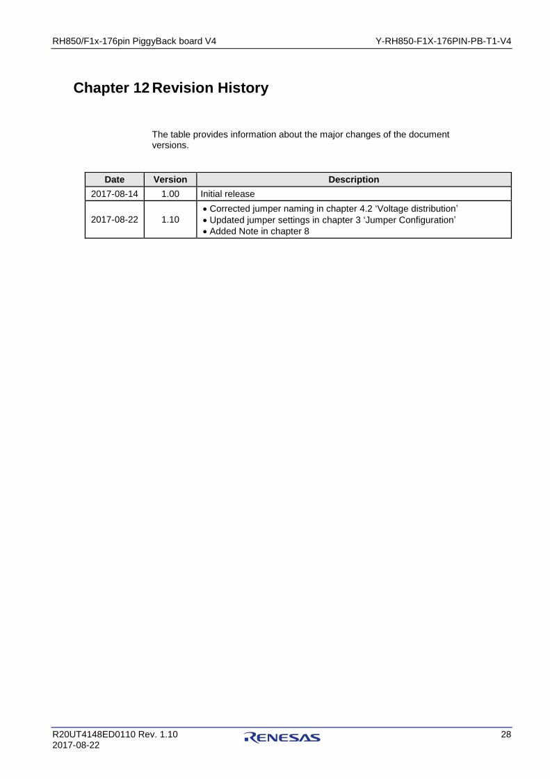
RH850/F1x-176pin PiggyBack board V4 Y-RH850-F1X-176PIN-PB-T1-V4
R20UT4148ED0110 Rev. 1.10 28 2017-08-22
Chapter 12 Revision History
The table provides information about the major changes of the document versions.
Date Version Description
2017-08-14 1.00 Initial release
2017-08-22 1.10
Corrected jumper naming in chapter 4.2 ‘Voltage distribution’
Updated jumper settings in chapter 3 ‘Jumper Configuration’
Added Note in chapter 8

Related Documents


![Guia Oficial Final Fantasy VIII [Piggyback]](https://static.cupdf.com/doc/110x72/55cf9bd2550346d033a77e40/guia-oficial-final-fantasy-viii-piggyback.jpg)