DEVICE PERFORMANCE SPECIFICATION Revision 1.0 MTD/PS-0938 January 30, 2006 KODAK KAI-11002 IMAGE SENSOR 4008(H) X 2672(V) INTERLINE CCD IMAGE SENSOR

Welcome message from author
This document is posted to help you gain knowledge. Please leave a comment to let me know what you think about it! Share it to your friends and learn new things together.
Transcript

DEVICE PERFORMANCE SPECIFICATION
Revision 1.0 MTD/PS-0938
January 30, 2006
KODAK KAI-11002 IMAGE SENSOR 4008(H) X 2672(V) INTERLINE CCD IMAGE SENSOR
TABLE OF CONTENTS
Summary Specification ...................................................................................................................................................................5 Device Description ..........................................................................................................................................................................6
Architecture.................................................................................................................................................................................6 Pixel .............................................................................................................................................................................................7 Vertical to Horizontal Tranfer .....................................................................................................................................................8 Horizontal Register to Floating Diffusion...................................................................................................................................9 Horizontal Register Split...........................................................................................................................................................10
Single Output Operation........................................................................................................................................................10 Dual Output Operation...........................................................................................................................................................10
Output ........................................................................................................................................................................................11 Pin Description and Physical Orientation.................................................................................................................................12
Performance .................................................................................................................................................................................13 Power - Estimated.....................................................................................................................................................................13 Frame Rates – Continuous Mode .............................................................................................................................................13 Imaging Performance ...............................................................................................................................................................14
Imaging Performance Operational Conditions ....................................................................................................................14 Imaging Performance Specifications ...................................................................................................................................14 Defect Definitions ..................................................................................................................................................................16 Quantum Efficiency................................................................................................................................................................17 Angular Quantum Efficiency .................................................................................................................................................19
Test Definitions .............................................................................................................................................................................20 Test Regions of Interest ............................................................................................................................................................20 OverClocking .............................................................................................................................................................................20 Tests...........................................................................................................................................................................................21
Operation .......................................................................................................................................................................................22 Maximum Ratings .....................................................................................................................................................................22 Maximum Voltage Ratings Between Pins ................................................................................................................................22 DC Bias Operating Conditions ..................................................................................................................................................22 AC Operating Conditions...........................................................................................................................................................23
Clock Levels...........................................................................................................................................................................23 Clock Line Capacitances.......................................................................................................................................................23
Timing Requirements................................................................................................................................................................23 Main Timing – Continuous Mode ..............................................................................................................................................24 Frame Timing – Continuous Mode ...........................................................................................................................................25
Frame Timing without Binning .............................................................................................................................................25 Frame Timing for Vertical Binning by 2................................................................................................................................25 Frame Timing Edge Alignment .............................................................................................................................................26
Line Timing – Continuous Mode ...............................................................................................................................................27 Line Timing Single Output.....................................................................................................................................................27 Line Timing Dual Output – Left Output.................................................................................................................................27 Line Timing Dual Output – Right Output ..............................................................................................................................28 Line Timing Vertical Binning by 2 .........................................................................................................................................28 Line Timing Detail .................................................................................................................................................................29 Line Timing Binning by 2 Detail ............................................................................................................................................29 Line Timing Edge Alignment.................................................................................................................................................30
Pixel Timing – Continuous Mode ..............................................................................................................................................31
©Eastman Kodak Company, 2006 www.kodak.com/go/imagers Revision 1.0 MTD/PS-0938 p2

Pixel Timing Detail.................................................................................................................................................................31 Fast Line Dump Timing.............................................................................................................................................................32 Electronic Shutter .....................................................................................................................................................................33
Electronic Shutter Line Timing.............................................................................................................................................33 Electronic Shutter – Integration Time Definition .................................................................................................................33 Electronic Shutter Description .............................................................................................................................................34
Storage and Handling ...................................................................................................................................................................35 Mechanical Drawings....................................................................................................................................................................36
Package .....................................................................................................................................................................................36 Die to Package Alignment.........................................................................................................................................................37 Glass ..........................................................................................................................................................................................38 Glass Transmission...................................................................................................................................................................39
Quality Assurance and Reliability.................................................................................................................................................40 Ordering Information ....................................................................................................................................................................41 Revision Changes..........................................................................................................................................................................42
©Eastman Kodak Company, 2006 www.kodak.com/go/imagers Revision 1.0 MTD/PS-0938 p3
TABLE OF FIGURES Figure 1: Sensor Architecture ........................................................................................................................................................6 Figure 2: Pixel Architecture............................................................................................................................................................7 Figure 3: Vertical to Horizontal Transfer Architecture..................................................................................................................8 Figure 4: Horizontal Register to Floating Diffusion Architecture .................................................................................................9 Figure 5: Horizontal Register .......................................................................................................................................................10 Figure 6: Output Architecture.......................................................................................................................................................11 Figure 7: Pin Description ..............................................................................................................................................................12 Figure 8: Power.............................................................................................................................................................................13 Figure 9: Frame Rates ..................................................................................................................................................................13 Figure 10: Color with Microlens Quantum Efficiency Using AR Glass .......................................................................................17 Figure 11: Color without Microlens Quantum Efficiency Using AR Glass ..................................................................................17 Figure 12: Monochrome with Microlens Quantum Efficiency .....................................................................................................18 Figure 13: Monochrome without Microlens Quantum Efficiency................................................................................................18 Figure 14: Monochrome with Lenslets Angular Quantum Efficiency .........................................................................................19 Figure 15: Color with Lenslets Angular Quantum Efficiency ......................................................................................................19 Figure 16: Overclock Regions of Interest.....................................................................................................................................20 Figure 17: Main Timing - Continuous Mode.................................................................................................................................24 Figure 18: Framing Timing without Binning ................................................................................................................................25 Figure 19: Frame Timing for Vertical Binning by 2......................................................................................................................25 Figure 20: Frame Timing Edge Alignment...................................................................................................................................26 Figure 21: Line Timing Single Output...........................................................................................................................................27 Figure 22: Line Timing Dual Output – Left Output.......................................................................................................................27 Figure 23: Line Timing Dual Output – Right Output ....................................................................................................................28 Figure 24: Line Timing Vertical Binning by 2 ...............................................................................................................................28 Figure 25: Line Timing Detail .......................................................................................................................................................29 Figure 26: Line Timing by 2 Detail................................................................................................................................................29 Figure 27: Line Timing Edge Alignment.......................................................................................................................................30 Figure 28: Pixel Timing .................................................................................................................................................................31 Figure 29: Pixel Timing Detail ......................................................................................................................................................31 Figure 30: Fast Line Dump Timing...............................................................................................................................................32 Figure 31: Electronic Shutter Line Timing...................................................................................................................................33 Figure 32: Integration Time Definition .........................................................................................................................................33 Figure 33: Package Drawing ........................................................................................................................................................36 Figure 34: Die to Package Alignment...........................................................................................................................................37 Figure 35: Glass Drawing .............................................................................................................................................................38 Figure 36: Glass Transmission.....................................................................................................................................................39
©Eastman Kodak Company, 2006 www.kodak.com/go/imagers Revision 1.0 MTD/PS-0938 p4
SUMMARY SPECIFICATION
KODAK KAI-11002 IMAGE SENSOR
4008 (H) X 2672 (V) INTERLINE TRANSFER PROGRESSIVE SCAN CCD
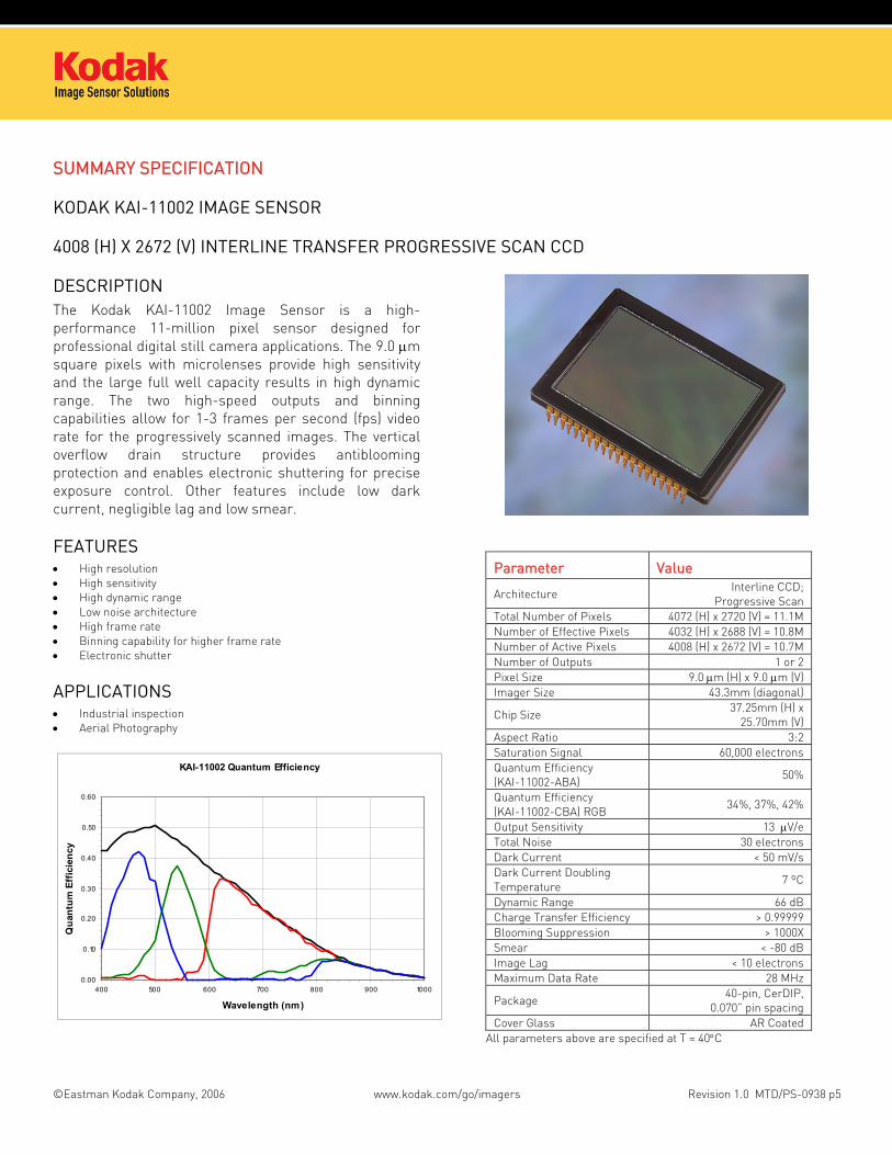
DESCRIPTION The Kodak KAI-11002 Image Sensor is a high-performance 11-million pixel sensor designed for professional digital still camera applications. The 9.0 µm square pixels with microlenses provide high sensitivity and the large full well capacity results in high dynamic range. The two high-speed outputs and binning capabilities allow for 1-3 frames per second (fps) video rate for the progressively scanned images. The vertical overflow drain structure provides antiblooming protection and enables electronic shuttering for precise exposure control. Other features include low dark current, negligible lag and low smear.
FEATURES • High resolution • High sensitivity • High dynamic range • Low noise architecture • High frame rate • Binning capability for higher frame rate • Electronic shutter
APPLICATIONS • Industrial inspection • Aerial Photography
KAI-11002 Quantum Efficiency
0.00
0.10
0.20
0.30
0.40
0.50
0.60
400 500 600 700 800 900 1000
Wavelength (nm)
Qua
ntum
Eff
icie
ncy
Parameter Value
Architecture Interline CCD;
Progressive Scan Total Number of Pixels 4072 (H) x 2720 (V) = 11.1M Number of Effective Pixels 4032 (H) x 2688 (V) = 10.8M Number of Active Pixels 4008 (H) x 2672 (V) = 10.7M Number of Outputs 1 or 2 Pixel Size 9.0 µm (H) x 9.0 µm (V) Imager Size 43.3mm (diagonal)
Chip Size 37.25mm (H) x
25.70mm (V) Aspect Ratio 3:2 Saturation Signal 60,000 electrons Quantum Efficiency (KAI-11002-ABA)
50%
Quantum Efficiency (KAI-11002-CBA) RGB
34%, 37%, 42%
Output Sensitivity 13 µV/e Total Noise 30 electrons Dark Current < 50 mV/s Dark Current Doubling Temperature
7 ºC
Dynamic Range 66 dB Charge Transfer Efficiency > 0.99999 Blooming Suppression > 1000X Smear < -80 dB Image Lag < 10 electrons Maximum Data Rate 28 MHz
Package 40-pin, CerDIP,
0.070” pin spacing Cover Glass AR Coated
All parameters above are specified at T = 40°C
©Eastman Kodak Company, 2006 www.kodak.com/go/imagers Revision 1.0 MTD/PS-0938 p5

DEVICE DESCRIPTION
ARCHITECTURE
4008 (H) x 2672 (V)Active Pixels
GGR
BG
GR
B
GGR
BG
GR
B
Pixel1,1
8 Buffer Rows
8 Buffer Rows
17 Dark Rows
16 Dark Rows
12 B
uffe
r Col
umns
13 B
uffe
r Col
umns
20 D
ark
Col
umns
19 D
ark
Col
umns
4 D
umm
y P
ixel
s
4 D
umm
y P
ixel
s
DualOutput
or
Video L Video R
4 20 12 4008 13 19 4Single
4 20 12 2004 2004 13 19 4
Fast Line Dump
Figure 1: Sensor Architecture
There are 17 light shielded rows followed 2688 photoactive rows and finally 16 more light shielded rows. The first 8 and the last 8 photoactive rows are buffer rows giving a total of 2672 lines of image data.
In the single output mode all pixels are clocked out of the Video L output in the lower left corner of the sensor. The first 4 empty pixels of each line do not receive charge from the vertical shift register. The next 20 pixels receive charge from the left light shielded edge followed by 4033 photosensitive pixels and finally 19 more light shielded pixels from the right edge of the sensor. The first 12 and last 13 photosensitive pixels are buffer pixels giving a total of 4008 pixels of image data.
In the dual output mode the clocking of the right half of the horizontal CCD is reversed. The left half of the image is clocked out Video L and the right half of the image is
clocked out Video R. For the Video L each row consists of 4 empty pixels followed by 20 light shielded pixels followed by 2016 photosensitive pixels. For the Video R each row consists of 4 empty pixels followed by 19 light shielded pixels followed by 2017 photosensitive pixels. When reconstructing the image, data from Video R will have to be reversed in a line buffer and appended to the Video L data.
The dark rows are not entirely dark and so should not be used for a dark reference level. Use the dark columns on the left or right side of the image sensor as a dark reference.
Of the dark columns, the first and last dark columns should not be used for determining the zero signal level. Some light does leak into the first and last dark columns.
©Eastman Kodak Company, 2006 www.kodak.com/go/imagers Revision 1.0 MTD/PS-0938 p6

PIXEL Top View
Directionof
ChargeTransfer
True Two Phase Burried Channel VCCDLightshield over VCCD not shown
9.0µm
V1Photodiode
9.0µm
V2TransferGate
Direction ofChargeTransfer
V1 V2 V1
n-n
n- n-
p Well (GND)
Cross Section Down Through VCCD
n Substrate
p
V1
np+
Light Shield
p
p
n
nSubstrate
p
Cross Section ThroughPhotodiode and VCCD Phase 1
Photodiode
p p
V2
np+
Light Shield
p
p
n
nSubstrate
p
Cross Section Through Photodiodeand VCCD Phase 2 at Transfer Gate
TransferGate
Cross Section Showing Lenslet
Lenslet
VCCD VCCDLight Shield Light Shield
Photodiode
Drawings not scale
Red Color Filter
Figure 2: Pixel Architecture
An electronic representation of an image is formed when incident photons falling on the sensor plane create electron-hole pairs within the individual silicon photodiodes. These photoelectrons are collected locally by the formation of potential wells at each photosite. Below photodiode saturation, the number of
photoelectrons collected at each pixel is linearly dependant upon light level and exposure time and non-linearly dependant on wavelength. When the photodiodes charge capacity is reached, excess electrons are discharged into the substrate to prevent blooming.
©Eastman Kodak Company, 2006 www.kodak.com/go/imagers Revision 1.0 MTD/PS-0938 p7

VERTICAL TO HORIZONTAL TRANFER Top View
Direction ofVerticalChargeTransfer
V1
V2
V1
Photodiode
V2TransferGate
FastLine
Dump
H1SH2S
H1B
H2B
Direction ofHorizontal
Charge Transfer
Lightshieldnot shown
Figure 3: Vertical to Horizontal Transfer Architecture
When the V1 and V2 timing inputs are pulsed, charge in every pixel of the VCCD is shifted one row towards the HCCD. The last row next to the HCCD is shifted into the HCCD. When the VCCD is shifted, the timing signals to the HCCD must be stopped. H1 must be stopped in the high state and H2 must be stopped in the low state. The HCCD clocking may begin THD µs after the falling edge of the V1 and V2 pulse.
Charge is transferred from the last vertical CCD phase into the H1S horizontal CCD phase. Refer to Figure 25 for an example of timing that accomplishes the vertical to horizontal transfer of charge.
If the fast line dump is held at the high level (FDH) during a vertical to horizontal transfer, then the entire line is removed and not transferred into the horizontal register.
©Eastman Kodak Company, 2006 www.kodak.com/go/imagers Revision 1.0 MTD/PS-0938 p8

HORIZONTAL REGISTER TO FLOATING DIFFUSION
n+
R OG H1 H2S H2B H1S H1B H2S
n- n- n-
RD
FloatingDiffusion
n (burried channel)nn+
p (GND)
n (SUB)
Figure 4: Horizontal Register to Floating Diffusion Architecture
The HCCD has a total of 4080 pixels. The 4072 vertical shift registers (columns) are shifted into the center 4072 pixels of the HCCD. There are 4 pixels at both ends of the HCCD, which receive no charge from a vertical shift register. The first 4 clock cycles of the HCCD will be empty pixels (containing no electrons). The next 20 clock cycles will contain only electrons generated by dark current in the VCCD and photodiodes. The next 4033 clock cycles will contain photo-electrons (image data). Finally, the last 19 clock cycles will contain only electrons generated by dark current in the VCCD and photodiodes. Of the 20 dark columns at the start of the line and the 19 dark columns at the end of the line, the first and last dark columns should not be used for determining the zero signal level. Some light does leak into the first and last dark columns. Only use the center 18 columns of the 20 column dark reference at the start
of the line. Only use the center 17 columns of the 19 column dark reference at the end of the line.
When the HCCD is shifting valid image data, the timing inputs to the electronic shutter (SUB), VCCD (V1, V2), and fast line dump (FD) should be not be pulsed. This prevents unwanted noise from being introduced. The HCCD is a type of charge coupled device known as a pseudo-two phase CCD. This type of CCD has the ability to shift charge in two directions. This allows the entire image to be shifted out to the video L output, or to the video R output (left/right image reversal). The HCCD is split into two equal halves of 2040 pixels each. When operating the sensor in single output mode the two halves of the HCCD are shifted in the same direction. When operating the sensor in dual output mode the two halves of the HCCD are shifted in opposite directions. The direction of charge transfer in each half is controlled by the H1BL, H2BL, H1BR, and H2BR timing inputs.
©Eastman Kodak Company, 2006 www.kodak.com/go/imagers Revision 1.0 MTD/PS-0938 p9
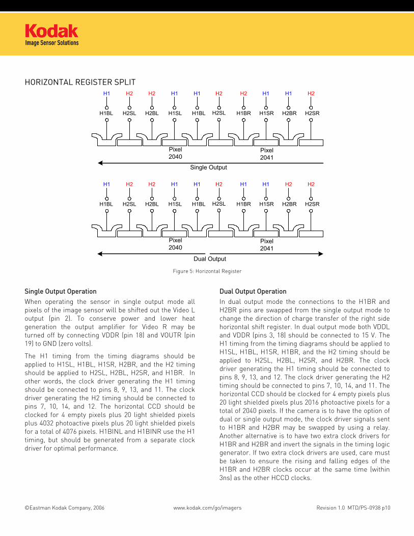
HORIZONTAL REGISTER SPLIT
Single Output
H2SLH1SL H1BL H2SRH1SR H2BRH1BR
Pixel2040
Pixel2041
H2SL H2BLH1BL
H1 H1 H1 H1 H1H2 H2 H2 H2 H2
H2SLH1SL H1BL H2SRH1SR H2BRH1BR
Pixel2040
Pixel2041
H2SL H2BLH1BL
H1 H1 H1 H1H1
Dual Output
H2H2 H2 H2 H2
Figure 5: Horizontal Register
Single Output Operation
When operating the sensor in single output mode all pixels of the image sensor will be shifted out the Video L output (pin 2). To conserve power and lower heat generation the output amplifier for Video R may be turned off by connecting VDDR (pin 18) and VOUTR (pin 19) to GND (zero volts).
The H1 timing from the timing diagrams should be applied to H1SL, H1BL, H1SR, H2BR, and the H2 timing should be applied to H2SL, H2BL, H2SR, and H1BR. In other words, the clock driver generating the H1 timing should be connected to pins 8, 9, 13, and 11. The clock driver generating the H2 timing should be connected to pins 7, 10, 14, and 12. The horizontal CCD should be clocked for 4 empty pixels plus 20 light shielded pixels plus 4032 photoactive pixels plus 20 light shielded pixels for a total of 4076 pixels. H1BINL and H1BINR use the H1 timing, but should be generated from a separate clock driver for optimal performance.
Dual Output Operation
In dual output mode the connections to the H1BR and H2BR pins are swapped from the single output mode to change the direction of charge transfer of the right side horizontal shift register. In dual output mode both VDDL and VDDR (pins 3, 18) should be connected to 15 V. The H1 timing from the timing diagrams should be applied to H1SL, H1BL, H1SR, H1BR, and the H2 timing should be applied to H2SL, H2BL, H2SR, and H2BR. The clock driver generating the H1 timing should be connected to pins 8, 9, 13, and 12. The clock driver generating the H2 timing should be connected to pins 7, 10, 14, and 11. The horizontal CCD should be clocked for 4 empty pixels plus 20 light shielded pixels plus 2016 photoactive pixels for a total of 2040 pixels. If the camera is to have the option of dual or single output mode, the clock driver signals sent to H1BR and H2BR may be swapped by using a relay. Another alternative is to have two extra clock drivers for H1BR and H2BR and invert the signals in the timing logic generator. If two extra clock drivers are used, care must be taken to ensure the rising and falling edges of the H1BR and H2BR clocks occur at the same time (within 3ns) as the other HCCD clocks.
©Eastman Kodak Company, 2006 www.kodak.com/go/imagers Revision 1.0 MTD/PS-0938 p10
OUTPUT
FloatingDiffusion
HCCDChargeTransfer
SourceFollower#1
SourceFollower#2
SourceFollower#3
RD
R
OG
H1BIN
H2S
H2B
H1S
H1B
VDD
VOUT
31 KΩ
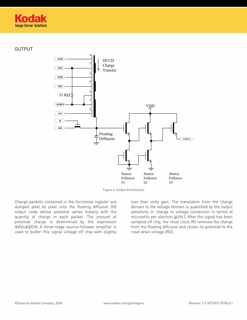
Figure 6: Output Architecture
Charge packets contained in the horizontal register are dumped pixel by pixel onto the floating diffusion (fd) output node whose potential varies linearly with the quantity of charge in each packet. The amount of potential charge is determined by the expression ∆Vfd=∆Q/Cfd. A three-stage source-follower amplifier is used to buffer this signal voltage off chip with slightly
less than unity gain. The translation from the charge domain to the voltage domain is quantified by the output sensitivity or charge to voltage conversion in terms of microvolts per electron (µV/e-). After the signal has been sampled off chip, the reset clock (R) removes the charge from the floating diffusion and resets its potential to the reset drain voltage (RD).
©Eastman Kodak Company, 2006 www.kodak.com/go/imagers Revision 1.0 MTD/PS-0938 p11

PIN DESCRIPTION AND PHYSICAL ORIENTATION
Pixel 1,1
1
RL
VO
UTL
VD
DL
OG
L
OG
R
GN
D
H1B
INL
GN
D
H2S
L
H1S
L
H1B
L
H2B
L
102 3 4 5 6 7 8 9 11 12 13 14 15 16 17 18 19 20
H2B
R
H1B
R
H1S
R
H2S
R
GN
D
H1B
INR
GN
D
VD
DR
VO
UTR R
R
2122232425262728293031323334353637383940
FD VR
DL
V1
V2
GN
D
SUB
GN
D
GN
D
GN
D
GN
D
GN
D
GN
D
ESD
GN
D
V1
V2
VR
DR
FD
Pin Name Description Pin Name Description 1 RL Reset Gate, Left 40 OGL Output Gate, Left 2 VOUTL Video Output, Left 39 FD Fast Line Dump Gate 3 VDDL Vdd, Left 38 RDL Reset Drain, Left 4 GND Ground 37 V1 Vertical Clock, Phase 1 5 H1BINL H1 Last Phase, Left 36 V2 Vertical Clock, Phase 2 6 GND Ground 35 GND Ground 7 H2SL H2 Storage, Left 34 SUB Substrate 8 H1SL H1 Storage, Left 33 GND Ground 9 H1BL H1 Barrier, Left 32 GND Ground 10 H2BL H2 Barrier, Left 31 GND Ground 11 H2BR H2 Barrier, Right 30 GND Ground 12 H1BR H1 Barrier, Right 29 GND Ground 13 H1SR H1 Storage, Right 28 GND Ground 14 H2SR H2 Storage, Right 27 ESD ESD Protection 15 GND Ground 26 GND Ground 16 H1BINR H1 Last Phase, Right 25 V1 Vertical Clock, Phase 1 17 GND Ground 24 V2 Vertical Clock, Phase 2 18 VDDR Vdd, Right 23 RDR Reset Drain, Right 19 VOUTR Video Output, Right 22 FD Fast Line Dump Gate 20 RR Reset Gate, Right 21 OGR Output Gate, Right
The pins are on a 0.070” spacing
Figure 7: Pin Description
©Eastman Kodak Company, 2006 www.kodak.com/go/imagers Revision 1.0 MTD/PS-0938 p12

PERFORMANCE
POWER - ESTIMATED
Right Output Disabled
0
50
100
150
200
250
300
350
400
450
500
0 5 10 15 20 25 30
Horizontal Clock Frequency (MHz)
Pow
er (m
W)
Output Pow er One Output(mW) Horizonatl Pow er (mW)
Vertical Pow er One Output(mW) Total Pow er One Output (mW)
Figure 8: Power
FRAME RATES – CONTINUOUS MODE
0
0.5
1
1.5
2
2.5
3
3.5
4
4.5
5
0 5 10 15 20 25 30
Pixel Clock (MHz)
Fram
e R
ate
(fps)
Dual output
Single output
Figure 9: Frame Rates
©Eastman Kodak Company, 2006 www.kodak.com/go/imagers Revision 1.0 MTD/PS-0938 p13

IMAGING PERFORMANCE
Imaging Performance Operational Conditions
Unless otherwise noted, the Imaging Performance Specifications are measured using the following conditions.
Description Condition Notes Frame Time 1732 msec 1 Horizontal Clock Frequency 10 MHz
Light Source Continuous red, green and blue illumination centered at 450, 530 and 650 nm
2,3
Operation Nominal operating voltages and timing Notes: 1. Electronic shutter is not used. Integration time equals frame time. 2. LEDs used: Blue: Nichia NLPB500, Green: Nichia NSPG500S and Red: HP HLMP-8115. 3. For monochrome sensor, only green LED used.
Imaging Performance Specifications KAI-11002-ABA Monochrome with Microlens and KAI-11002-CBA Color with Microlens
Description Symbol Min. Nom. Max. Units Samp-
ling Plan
Tempera-ture
Tested At (°C)
Notes Test
Maximum Photoresponse Nonlinearity
NL n/a 2 % Design 2, 3
Maximum Gain Difference Between Outputs
∆G n/a 10 % Design 2, 3
Max. Signal Error due to Nonlinearity Dif.
∆NL n/a 1 % Design 2, 3
Horizontal CCD Charge Capacity
HNe 139 ke- Design
Vertical CCD Charge Capacity VNe 90 91 ke- Die Photodiode Charge Capacity PNe 58 60 ke- Die Horizontal CCD Charge Transfer Efficiency
HCTE 0.99999 n/a Design
Vertical CCD Charge Transfer Efficiency
VCTE 0.99999 n/a Design
Photodiode Dark Current Ipd n/a 800 e/p/s Die 27, 40 Photodiode Dark Current Ipd n/a 0.15 nA/cm2 Die 27, 40 Vertical CCD Dark Current Ivd n/a 3800 e/p/s Die 27, 40 Vertical CCD Dark Current Ivd n/a 0.5 nA/cm2 Die 27, 40 Image Lag Lag n/a <10 50 e- Design Antiblooming Factor Xab 100 300 n/a Design Vertical Smear Smr n/a -85 -75 dB Design Total Noise ne-T 30 e-rms Design 4 Dynamic Range DR 66 dB Design 5 Output Amplifier DC Offset Vodc 4 9 14 V Die Output Amplifier Bandwidth F-3db 106 MHz Die 6 Output Amplifier Impedance ROUT 100 150 200 Ohms Die Output Amplifier Sensitivity ∆V/∆N 13 µV/e- Design
©Eastman Kodak Company, 2006 www.kodak.com/go/imagers Revision 1.0 MTD/PS-0938 p14
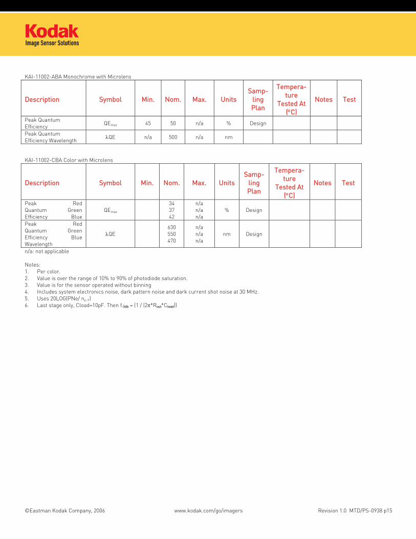
KAI-11002-ABA Monochrome with Microlens
Description Symbol Min. Nom. Max. Units Samp-
ling Plan
Tempera-ture
Tested At (°C)
Notes Test
Peak Quantum Efficiency
QEmax 45 50 n/a % Design
Peak Quantum Efficiency Wavelength
λQE n/a 500 n/a nm
KAI-11002-CBA Color with Microlens
Description Symbol Min. Nom. Max. Units Samp-
ling Plan
Tempera-ture
Tested At (°C)
Notes Test
Peak Red Quantum Green Efficiency Blue
QEmax 34 37 42
n/a n/a n/a
% Design
Peak Red Quantum Green Efficiency Blue Wavelength
λQE 630 550 470
n/a n/a n/a
nm Design
n/a: not applicable Notes: 1. Per color. 2. Value is over the range of 10% to 90% of photodiode saturation. 3. Value is for the sensor operated without binning 4. Includes system electronics noise, dark pattern noise and dark current shot noise at 30 MHz. 5. Uses 20LOG(PNe/ ne-T) 6. Last stage only, Cload=10pF. Then f-3db = (1 / (2π*Rout*Cload))
©Eastman Kodak Company, 2006 www.kodak.com/go/imagers Revision 1.0 MTD/PS-0938 p15
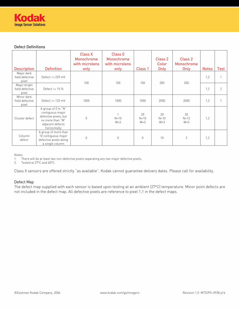
Defect Definitions
Description Definition
Class X Monochrome
with microlens only
Class 0 Monochrome
with microlens only Class 1
Class 2 Color Only
Class 2 Monochrome
Only Notes Test Major dark
field defective pixel
Defect >= 239 mV 1,2 1
Major bright field defective
pixel Defect >= 15 %
100 100 100 200 200
1,2 2
Minor dark field defective
pixel Defect >= 123 mV 1000 1000 1000 2000 2000 1,2 1
Cluster defect
A group of 2 to “N” contiguous major
defective pixels, but no more than “W” adjacent defects
horizontally
0 1
N=10 W=3
20 N=10 W=3
20 N=10 W=3
20 N=12 W=5
1,2
Column defect
A group of more than 10 contiguous major defective pixels along
a single column
0 0 0 10 2 1,2
Notes: 1. There will be at least two non-defective pixels separating any two major defective pixels. 2. Tested at 27°C and 40°C. Class X sensors are offered strictly “as available”. Kodak cannot guarantee delivery dates. Please call for availability.
Defect Map The defect map supplied with each sensor is based upon testing at an ambient (27°C) temperature. Minor point defects are not included in the defect map. All defective pixels are reference to pixel 1,1 in the defect maps.
©Eastman Kodak Company, 2006 www.kodak.com/go/imagers Revision 1.0 MTD/PS-0938 p16
Quantum Efficiency Color with Microlens Quantum Efficiency
0.00
0.05
0.10
0.15
0.20
0.25
0.30
0.35
0.40
0.45
400 500 600 700 800 900 1000
Wavelength (nm)
Abs
olut
e Q
uant
um E
ffici
ency
Red Green Blue
Figure 10: Color with Microlens Quantum Efficiency Using AR Glass
Color without Microlens Quantum Efficiency
0.00
0.02
0.04
0.06
0.08
0.10
0.12
0.14
0.16
0.18
400 500 600 700 800 900 1000
Wavelength (nm)
Abs
olut
e Q
uant
um E
ffici
ency
Red Green Blue
Figure 11: Color without Microlens Quantum Efficiency Using AR Glass
©Eastman Kodak Company, 2006 www.kodak.com/go/imagers Revision 1.0 MTD/PS-0938 p17
Monochrome with Microlens Quantum Efficiency
0.00
0.10
0.20
0.30
0.40
0.50
0.60
300 400 500 600 700 800 900 1000
Wavelength (nm)
Abs
olut
e Q
uant
um E
ffic
ienc
y
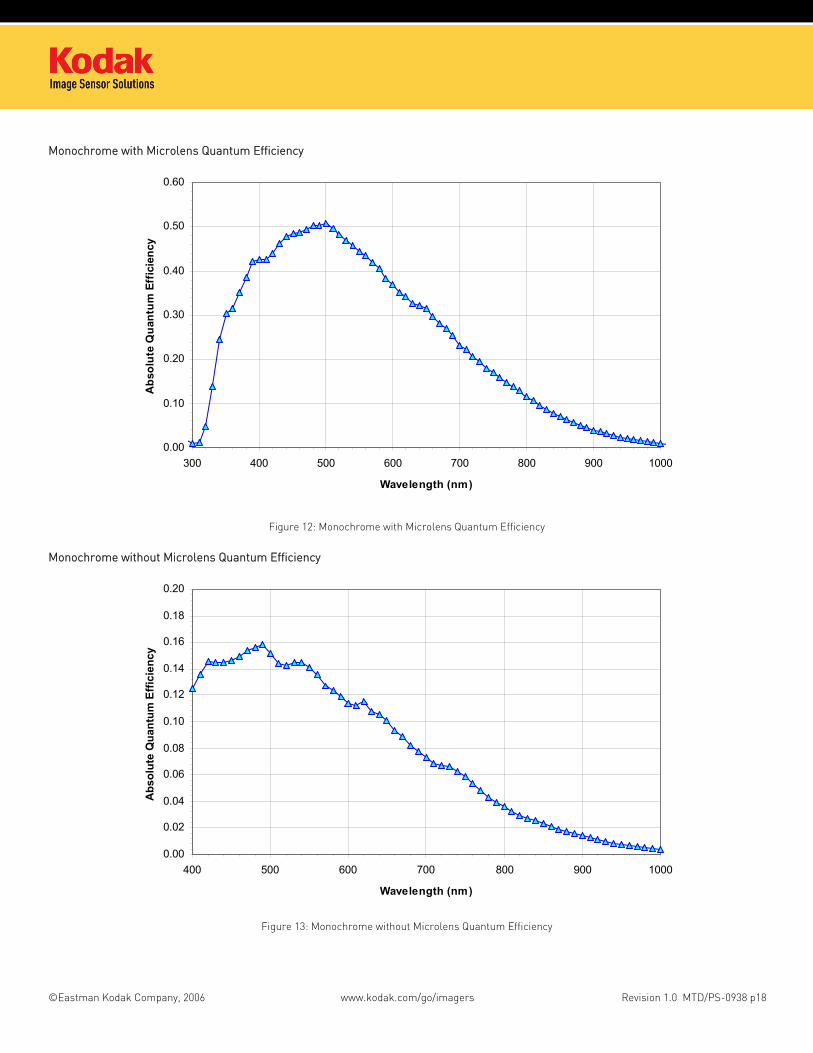
Figure 12: Monochrome with Microlens Quantum Efficiency
Monochrome without Microlens Quantum Efficiency
0.00
0.02
0.04
0.06
0.08
0.10
0.12
0.14
0.16
0.18
0.20
400 500 600 700 800 900 1000
Wavelength (nm)
Abs
olut
e Q
uant
um E
ffici
ency
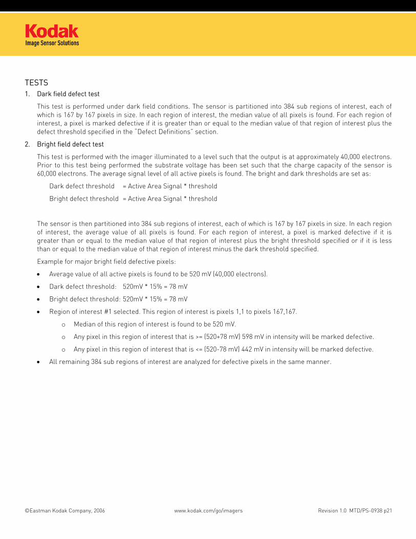
Figure 13: Monochrome without Microlens Quantum Efficiency
©Eastman Kodak Company, 2006 www.kodak.com/go/imagers Revision 1.0 MTD/PS-0938 p18

Angular Quantum Efficiency
For the curves marked “Horizontal”, the incident light angle is varied in a plane parallel to the HCCD. For the curves marked “Vertical”, the incident light angle is varied in a plane parallel to the VCCD.
Monochrome with Lenslets
0%
10%
20%
30%
40%
50%
60%
70%
80%
90%
100%
0 5 10 15 20 25 30
Angle (degress)
Rel
ativ
e Q
uant
um E
ffici
ency
(%) Vertical
Horizontal
Figure 14: Monochrome with Lenslets Angular Quantum Efficiency
Color with Lenslets
0%
10%
20%
30%
40%
50%
60%
70%
80%
90%
100%
-25 -20 -15 -10 -5 0 5 10 15 20 25
Angle (degress)
Rel
ativ
e Q
uant
um E
ffici
ency
RedGreenBlueVertical
Horizontal
Vertical
Figure 15: Color with Lenslets Angular Quantum Efficiency
©Eastman Kodak Company, 2006 www.kodak.com/go/imagers Revision 1.0 MTD/PS-0938 p19

TEST DEFINITIONS
TEST REGIONS OF INTEREST Active Area ROI: Pixel 1, 1 to Pixel 4008,2672
Center 100 by 100 ROI: Pixel 1954,1336 to Pixel 2053,1435
Only the active pixels are used for performance and defect tests.
OVERCLOCKING The test system timing is configured such that the sensor is overclocked in both the vertical and horizontal directions. See Figure 16 for a pictorial representation of the regions.
Pixel 1,1
Vertical Overclock
Hor
izon
tal O
verc
lock
H
V
Figure 16: Overclock Regions of Interest
©Eastman Kodak Company, 2006 www.kodak.com/go/imagers Revision 1.0 MTD/PS-0938 p20
TESTS 1. Dark field defect test
This test is performed under dark field conditions. The sensor is partitioned into 384 sub regions of interest, each of which is 167 by 167 pixels in size. In each region of interest, the median value of all pixels is found. For each region of interest, a pixel is marked defective if it is greater than or equal to the median value of that region of interest plus the defect threshold specified in the “Defect Definitions” section.
2. Bright field defect test
This test is performed with the imager illuminated to a level such that the output is at approximately 40,000 electrons. Prior to this test being performed the substrate voltage has been set such that the charge capacity of the sensor is 60,000 electrons. The average signal level of all active pixels is found. The bright and dark thresholds are set as:
Dark defect threshold = Active Area Signal * threshold
Bright defect threshold = Active Area Signal * threshold
The sensor is then partitioned into 384 sub regions of interest, each of which is 167 by 167 pixels in size. In each region of interest, the average value of all pixels is found. For each region of interest, a pixel is marked defective if it is greater than or equal to the median value of that region of interest plus the bright threshold specified or if it is less than or equal to the median value of that region of interest minus the dark threshold specified.
Example for major bright field defective pixels:
• Average value of all active pixels is found to be 520 mV (40,000 electrons).
• Dark defect threshold: 520mV * 15% = 78 mV
• Bright defect threshold: 520mV * 15% = 78 mV
• Region of interest #1 selected. This region of interest is pixels 1,1 to pixels 167,167.
o Median of this region of interest is found to be 520 mV.
o Any pixel in this region of interest that is >= (520+78 mV) 598 mV in intensity will be marked defective.
o Any pixel in this region of interest that is <= (520-78 mV) 442 mV in intensity will be marked defective.
• All remaining 384 sub regions of interest are analyzed for defective pixels in the same manner.
©Eastman Kodak Company, 2006 www.kodak.com/go/imagers Revision 1.0 MTD/PS-0938 p21
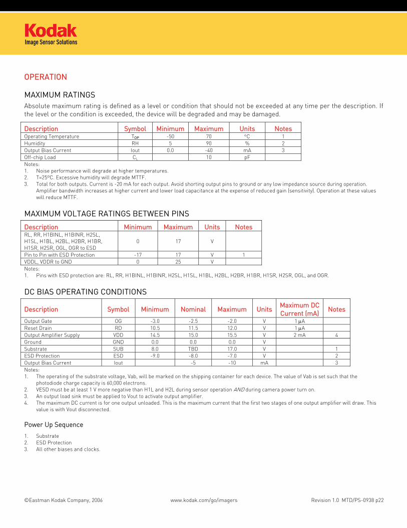
OPERATION
MAXIMUM RATINGS Absolute maximum rating is defined as a level or condition that should not be exceeded at any time per the description. If the level or the condition is exceeded, the device will be degraded and may be damaged.
Description Symbol Minimum Maximum Units Notes Operating Temperature TOP -50 70 °C 1 Humidity RH 5 90 % 2 Output Bias Current Iout 0.0 -40 mA 3 Off-chip Load CL 10 pF Notes: 1. Noise performance will degrade at higher temperatures. 2. T=25ºC. Excessive humidity will degrade MTTF. 3. Total for both outputs. Current is -20 mA for each output. Avoid shorting output pins to ground or any low impedance source during operation.
Amplifier bandwidth increases at higher current and lower load capacitance at the expense of reduced gain (sensitivity). Operation at these values will reduce MTTF.
MAXIMUM VOLTAGE RATINGS BETWEEN PINS
Description Minimum Maximum Units Notes RL, RR, H1BINL, H1BINR, H2SL, H1SL, H1BL, H2BL, H2BR, H1BR, H1SR, H2SR, OGL, OGR to ESD
0 17 V
Pin to Pin with ESD Protection -17 17 V 1 VDDL, VDDR to GND 0 25 V Notes: 1. Pins with ESD protection are: RL, RR, H1BINL, H1BINR, H2SL, H1SL, H1BL, H2BL, H2BR, H1BR, H1SR, H2SR, OGL, and OGR.
DC BIAS OPERATING CONDITIONS
Description Symbol Minimum Nominal Maximum Units Maximum DC Current (mA)
Notes
Output Gate OG -3.0 -2.5 -2.0 V 1 µA Reset Drain RD 10.5 11.5 12.0 V 1 µA Output Amplifier Supply VDD 14.5 15.0 15.5 V 2 mA 4 Ground GND 0.0 0.0 0.0 V Substrate SUB 8.0 TBD 17.0 V 1 ESD Protection ESD -9.0 -8.0 -7.0 V 2 Output Bias Current Iout -5 -10 mA 3 Notes: 1. The operating of the substrate voltage, Vab, will be marked on the shipping container for each device. The value of Vab is set such that the
photodiode charge capacity is 60,000 electrons. 2. VESD must be at least 1 V more negative than H1L and H2L during sensor operation AND during camera power turn on. 3. An output load sink must be applied to Vout to activate output amplifier. 4. The maximum DC current is for one output unloaded. This is the maximum current that the first two stages of one output amplifier will draw. This
value is with Vout disconnected. Power Up Sequence
1. Substrate 2. ESD Protection 3. All other biases and clocks.
©Eastman Kodak Company, 2006 www.kodak.com/go/imagers Revision 1.0 MTD/PS-0938 p22
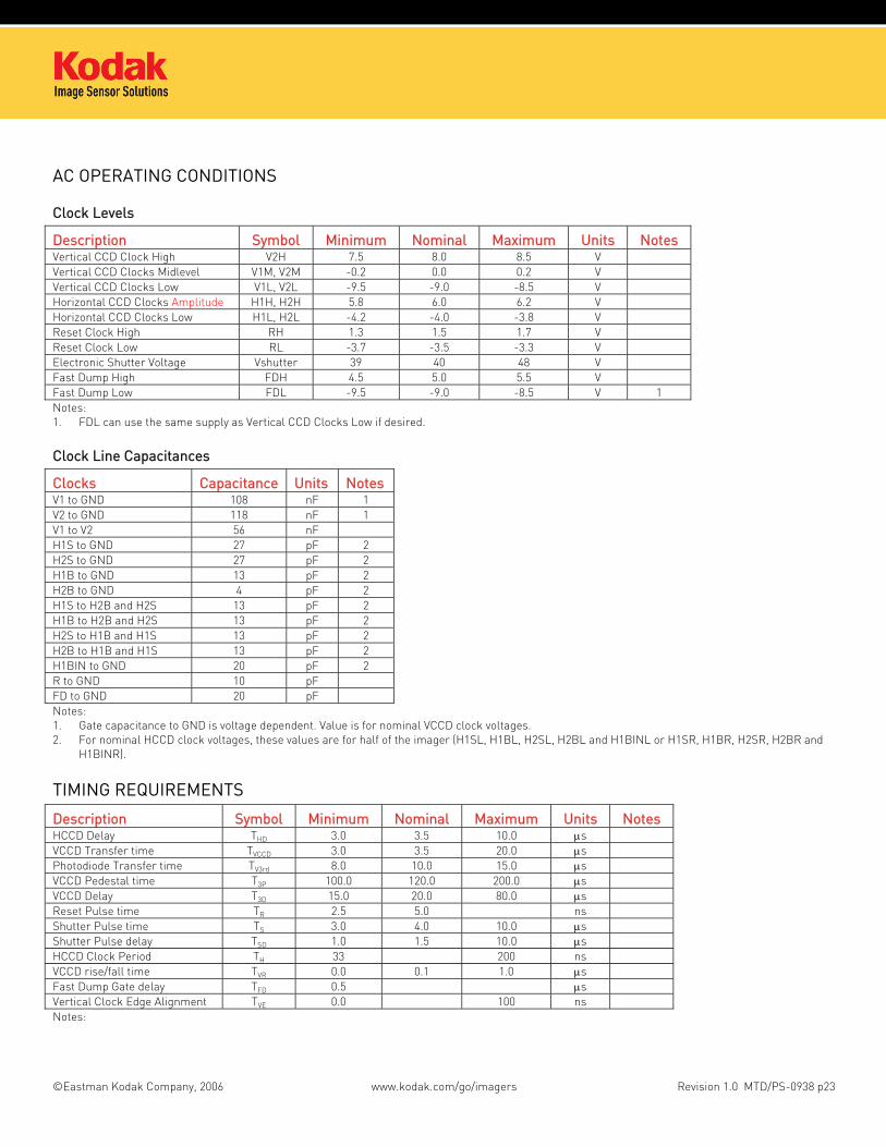
AC OPERATING CONDITIONS
Clock Levels
Description Symbol Minimum Nominal Maximum Units Notes Vertical CCD Clock High V2H 7.5 8.0 8.5 V Vertical CCD Clocks Midlevel V1M, V2M -0.2 0.0 0.2 V Vertical CCD Clocks Low V1L, V2L -9.5 -9.0 -8.5 V Horizontal CCD Clocks Amplitude H1H, H2H 5.8 6.0 6.2 V Horizontal CCD Clocks Low H1L, H2L -4.2 -4.0 -3.8 V Reset Clock High RH 1.3 1.5 1.7 V Reset Clock Low RL -3.7 -3.5 -3.3 V Electronic Shutter Voltage Vshutter 39 40 48 V Fast Dump High FDH 4.5 5.0 5.5 V Fast Dump Low FDL -9.5 -9.0 -8.5 V 1 Notes: 1. FDL can use the same supply as Vertical CCD Clocks Low if desired.
Clock Line Capacitances
Clocks Capacitance Units Notes V1 to GND 108 nF 1 V2 to GND 118 nF 1 V1 to V2 56 nF H1S to GND 27 pF 2 H2S to GND 27 pF 2 H1B to GND 13 pF 2 H2B to GND 4 pF 2 H1S to H2B and H2S 13 pF 2 H1B to H2B and H2S 13 pF 2 H2S to H1B and H1S 13 pF 2 H2B to H1B and H1S 13 pF 2 H1BIN to GND 20 pF 2 R to GND 10 pF FD to GND 20 pF Notes: 1. Gate capacitance to GND is voltage dependent. Value is for nominal VCCD clock voltages. 2. For nominal HCCD clock voltages, these values are for half of the imager (H1SL, H1BL, H2SL, H2BL and H1BINL or H1SR, H1BR, H2SR, H2BR and
H1BINR).
TIMING REQUIREMENTS
Description Symbol Minimum Nominal Maximum Units Notes HCCD Delay THD 3.0 3.5 10.0 µs VCCD Transfer time TVCCD 3.0 3.5 20.0 µs Photodiode Transfer time TV3rd 8.0 10.0 15.0 µs VCCD Pedestal time T3P 100.0 120.0 200.0 µs VCCD Delay T3D 15.0 20.0 80.0 µs Reset Pulse time TR 2.5 5.0 ns Shutter Pulse time TS 3.0 4.0 10.0 µs Shutter Pulse delay TSD 1.0 1.5 10.0 µs HCCD Clock Period TH 33 200 ns VCCD rise/fall time TVR 0.0 0.1 1.0 µs Fast Dump Gate delay TFD 0.5 µs Vertical Clock Edge Alignment TVE 0.0 100 ns Notes:
©Eastman Kodak Company, 2006 www.kodak.com/go/imagers Revision 1.0 MTD/PS-0938 p23
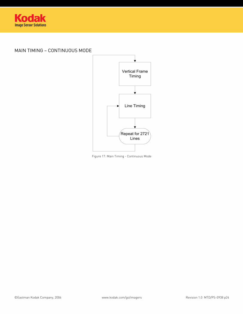
MAIN TIMING – CONTINUOUS MODE
Vertical FrameTiming
Line Timing
Repeat for 2721Lines
Figure 17: Main Timing - Continuous Mode
©Eastman Kodak Company, 2006 www.kodak.com/go/imagers Revision 1.0 MTD/PS-0938 p24

FRAME TIMING – CONTINUOUS MODE
Frame Timing without Binning
H2L
V1
V2
H1, H1BIN
H2
TL TV3rd
T3P T3D
TL
Line 2721 Line 12720 H1H, H1BINH
H1L, H1BINLH2H
V2L
V2M
V1L
V1M
V1H
Figure 18: Framing Timing without Binning
Frame Timing for Vertical Binning by 2
V1
V2
H1, H1BIN
H2
TL TV3rd
T3P T3D
TL
Line 1361 Line 1Line 1360
3 x TVCCD
Figure 19: Frame Timing for Vertical Binning by 2
©Eastman Kodak Company, 2006 www.kodak.com/go/imagers Revision 1.0 MTD/PS-0938 p25

Frame Timing Edge Alignment
V1
V2TVE
V1M
V1L
V2H
V2M
V2L
Figure 20: Frame Timing Edge Alignment
©Eastman Kodak Company, 2006 www.kodak.com/go/imagers Revision 1.0 MTD/PS-0938 p26
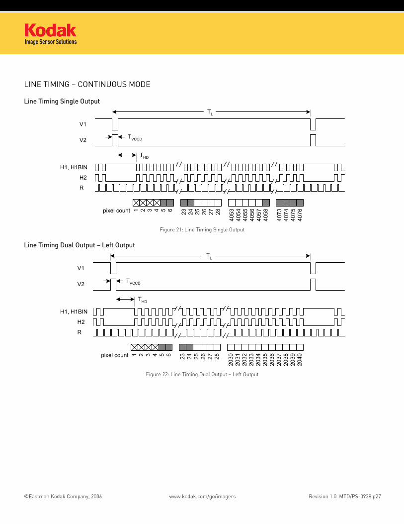
LINE TIMING – CONTINUOUS MODE
Line Timing Single Output
V1
V2 TVCCD
TL
THD
H1, H1BIN
H2
R232 3 4 5 6 24 25 26 27
4053
4054
4055
4057
4058
4074
40751pixel count 28
4056
4073
4076
Figure 21: Line Timing Single Output
Line Timing Dual Output – Left Output
V1
V2 TVCCD
TL
THD
H1, H1BIN
H2
R
232 3 4 5 6 24 25 26 27
2030
2031
2032
2034
2035
2038
20391pixel count 28
2033
2037
2040
2036
Figure 22: Line Timing Dual Output – Left Output
©Eastman Kodak Company, 2006 www.kodak.com/go/imagers Revision 1.0 MTD/PS-0938 p27

Line Timing Dual Output – Right Output
V1
V2 TVCCD
TL
THD
H1, H1BIN
H2
R
232 3 4 5 6 24 25 26 27
2030
2031
2032
2034
2035
2038
20391pixel count 28
2033
2037
2040
2036
Figure 23: Line Timing Dual Output – Right Output
Line Timing Vertical Binning by 2
V1
V2TVCCD
TL
THD
H1, H1BIN
H2
R
232 3 4 5 24 25 26 27
4053
4054
4055
4057
4058
4074
40751pixel count 28
4056
4073
4076
Figure 24: Line Timing Vertical Binning by 2
©Eastman Kodak Company, 2006 www.kodak.com/go/imagers Revision 1.0 MTD/PS-0938 p28
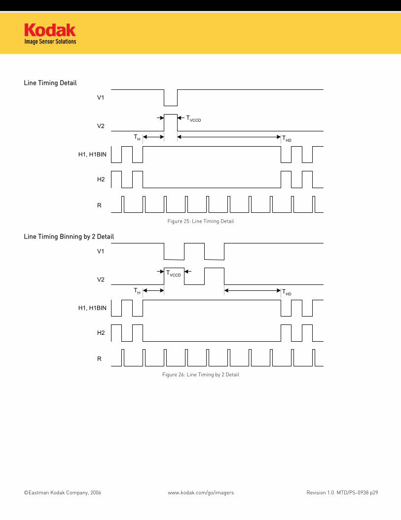
Line Timing Detail
V1
V2TVCCD
H2
H1, H1BIN
THDTH
R
Figure 25: Line Timing Detail
Line Timing Binning by 2 Detail
V1
V2TVCCD
H2
H1, H1BIN
THDTH
R
Figure 26: Line Timing by 2 Detail
©Eastman Kodak Company, 2006 www.kodak.com/go/imagers Revision 1.0 MTD/PS-0938 p29

Line Timing Edge Alignment
V1
V2
TVE TVE
TVCCD
Figure 27: Line Timing Edge Alignment
©Eastman Kodak Company, 2006 www.kodak.com/go/imagers Revision 1.0 MTD/PS-0938 p30
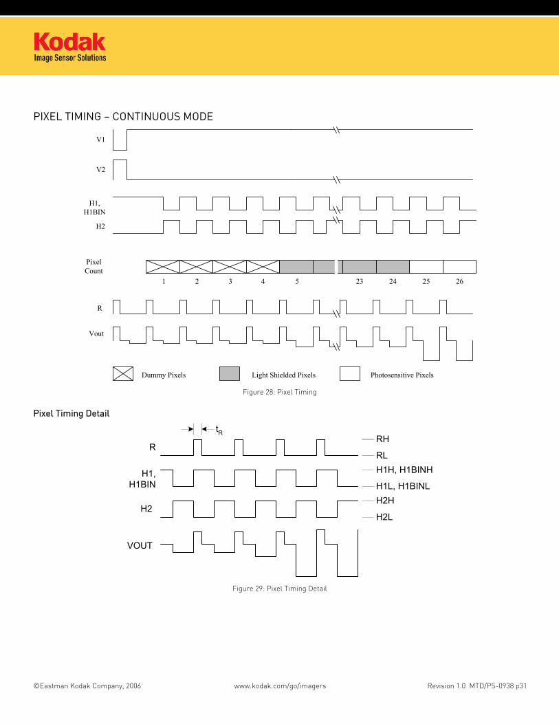
PIXEL TIMING – CONTINUOUS MODE
H1,H1BIN
H2
R
Vout
V1
V2
1 2 3 4 5
PixelCount
23 24 25 26
Dummy Pixels Light Shielded Pixels Photosensitive Pixels Figure 28: Pixel Timing
Pixel Timing Detail
R
H1,H1BIN
H2
VOUT
tRRH
RLH1H, H1BINH
H1L, H1BINLH2H
H2L
Figure 29: Pixel Timing Detail
©Eastman Kodak Company, 2006 www.kodak.com/go/imagers Revision 1.0 MTD/PS-0938 p31
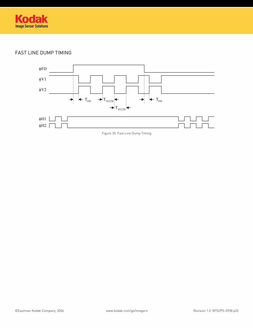
FAST LINE DUMP TIMING
TVCCD
φV1
φV2
TFD
φFD
TFDTVCCD
φH1φH2
Figure 30: Fast Line Dump Timing
©Eastman Kodak Company, 2006 www.kodak.com/go/imagers Revision 1.0 MTD/PS-0938 p32
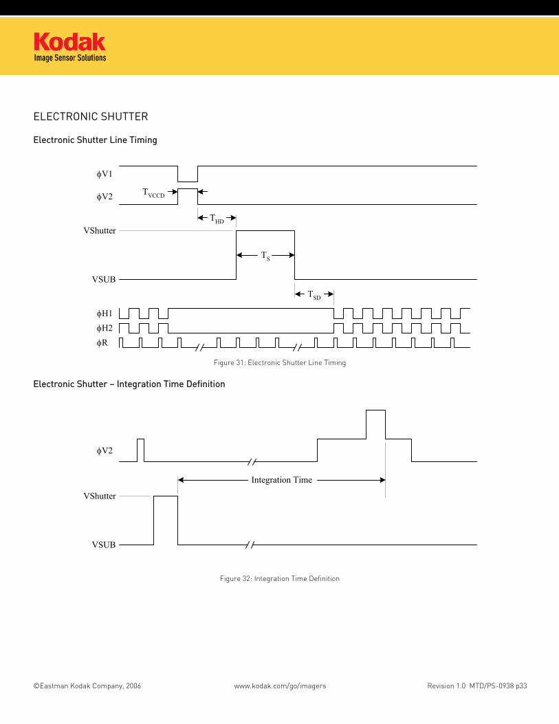
ELECTRONIC SHUTTER
Electronic Shutter Line Timing
φV1
φV2 TVCCD
TS
THD
φH1φH2φR
TSD
VShutter
VSUB
Figure 31: Electronic Shutter Line Timing
Electronic Shutter – Integration Time Definition
φV2
Integration Time
VShutter
VSUB
Figure 32: Integration Time Definition
©Eastman Kodak Company, 2006 www.kodak.com/go/imagers Revision 1.0 MTD/PS-0938 p33

Electronic Shutter Description
The voltage on the substrate (SUB) determines the charge capacity of the photodiodes. When SUB is 8 volts the photodiodes will be at their maximum charge capacity. Increasing VSUB above 8 volts decreases the charge capacity of the photodiodes until 40 volts when the photodiodes have a charge capacity of zero electrons. Therefore, a short pulse on SUB, with a peak amplitude greater than 40 volts, empties all photodiodes and provides the electronic shuttering action.
It may appear the optimal substrate voltage setting is 8 volts to obtain the maximum charge capacity and dynamic range. While setting VSUB to 8 volts will provide the maximum dynamic range, it will also provide the minimum antiblooming protection.
The KAI-11002 VCCD has a charge capacity of 90,000 electrons (90 ke-). If the SUB voltage is set such that the photodiode holds more than 90 ke-, then when the charge is transferred from a full photodiode to VCCD, the VCCD will overflow. This overflow condition manifests itself in the image by making bright spots appear elongated in the vertical direction. The size increase of a bright spot is called blooming when the spot doubles in size.
The blooming can be eliminated by increasing the voltage on SUB to lower the charge capacity of the photodiode. This ensures the VCCD charge capacity is greater than the photodiode capacity. There are cases where an extremely bright spot will still cause blooming in the VCCD. Normally, when the photodiode is full, any additional electrons generated by photons will spill out of the photodiode. The excess electrons are drained
harmlessly out to the substrate. There is a maximum rate at which the electrons can be drained to the substrate. If that maximum rate is exceeded, (for example, by a very bright light source) then it is possible for the total amount of charge in the photodiode to exceed the VCCD capacity. This results in blooming.
The amount of antiblooming protection also decreases when the integration time is decreased. There is a compromise between photodiode dynamic range (controlled by VSUB) and the amount of antiblooming protection. A low VSUB voltage provides the maximum dynamic range and minimum (or no) antiblooming protection. A high VSUB voltage provides lower dynamic range and maximum antiblooming protection. The optimal setting of VSUB is written on the container in which each KAI-11002 is shipped. The given VSUB voltage for each sensor is selected to provide antiblooming protection for bright spots at least 100 times saturation, while maintaining at least 60 ke- of dynamic range.
The electronic shutter provides a method of precisely controlling the image exposure time without any mechanical components. If an integration time of TINT is desired, then the substrate voltage of the sensor is pulsed to at least 40 volts TINT seconds before the photodiode to VCCD transfer pulse on V2. Use of the electronic shutter does not have to wait until the previously acquired image has been completely read out of the VCCD.
©Eastman Kodak Company, 2006 www.kodak.com/go/imagers Revision 1.0 MTD/PS-0938 p34
STORAGE AND HANDLING Storage Conditions
Description Symbol Minimum Maximum Units Notes Storage
Temperature TST -20 80 °C 1
Humidity RH 5 90 % 2 Notes: 1. Long-term exposure toward the maximum temperature will accelerate color filter degradation. 2. T=25ºC. Excessive humidity will degrade MTTF.
ESD
1. This device contains limited protection against Electrostatic Discharge (ESD). CCD image sensors can be damaged by electrostatic discharge. Failure to do so may alter device performance and reliability.
2. Devices should be handled in accordance with strict ESD procedures for Class 0 (<250V per JESD22 Human Body Model test), or Class A (<200V JESD22 Machine Model test) devices.
Devices are shipped in static-safe containers and should only be handled at static-safe workstations.
3. See Application Note MTD/PS-0224 “Electrostatic Discharge Control for Image Sensors” for proper handling and grounding procedures. This application note also contains recommendations for workplace modifications for the minimization of electrostatic discharge.
4. Store devices in containers made of electro-conductive materials.
Cover Glass Care and Cleanliness
1. The cover glass is highly susceptible to particles and other contamination. Perform all assembly operations in a clean environment.
2. Touching the cover glass must be avoided
3. Improper cleaning of the cover glass may damage these devices. Refer to Application Note MTD/PS-0237 “Cover Glass Cleaning for Image Sensors”
Environmental Exposure
1. Do not expose to strong sun light for long periods of time. The color filters and/or microlenses may become discolored. Long time exposures to a static high contrast scene should be avoided. The image sensor may become discolored and localized changes in response may occur from color filter/microlens aging.
2. Exposure to temperatures exceeding the absolute maximum levels should be avoided for storage and operation. Failure to do so may alter device performance and reliability.
3. Avoid sudden temperature changes.
4. Exposure to excessive humidity will affect device characteristics and should be avoided. Failure to do so may alter device performance and reliability.
5. Avoid storage of the product in the presence of dust or corrosive agents or gases.
Long-term storage should be avoided. Deterioration of lead solderability may occur. It is advised that the solderability of the device leads be re-inspected after an extended period of storage, over one year.
Soldering Recommendations
1. The soldering iron tip temperature is not to exceed 370ºC. Failure to do so may alter device performance and reliability.
2. Flow soldering method is not recommended. Solder dipping can cause damage to the glass and harm the imaging capability of the device. Recommended method is by partial heating. Kodak recommends the use of a grounded 30W soldering iron. Heat each pin for less than 2 seconds duration.
©Eastman Kodak Company, 2006 www.kodak.com/go/imagers Revision 1.0 MTD/PS-0938 p35
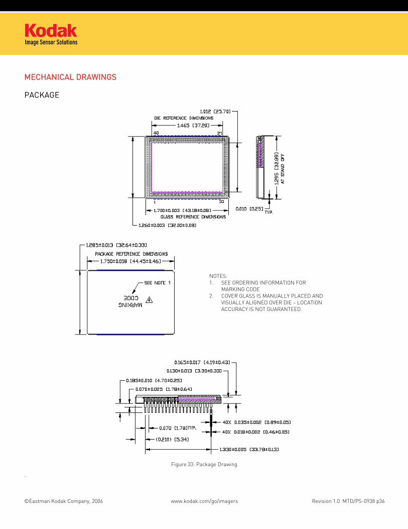
MECHANICAL DRAWINGS
PACKAGE
NOTES: 1. SEE ORDERING INFORMATION FOR
MARKING CODE 2. COVER GLASS IS MANUALLY PLACED AND
VISUALLY ALIGNED OVER DIE – LOCATION ACCURACY IS NOT GUARANTEED.
Figure 33: Package Drawing
.
©Eastman Kodak Company, 2006 www.kodak.com/go/imagers Revision 1.0 MTD/PS-0938 p36
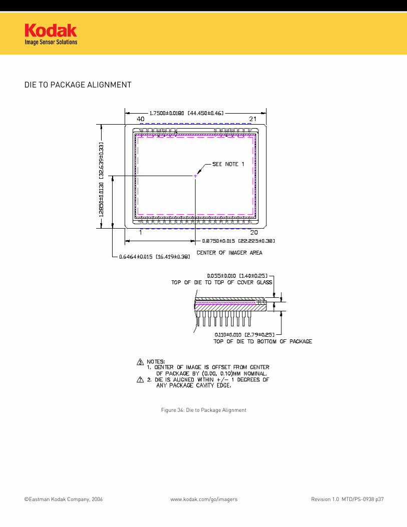
DIE TO PACKAGE ALIGNMENT
Figure 34: Die to Package Alignment
©Eastman Kodak Company, 2006 www.kodak.com/go/imagers Revision 1.0 MTD/PS-0938 p37
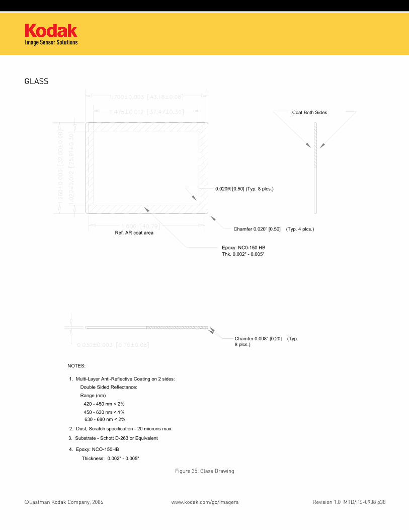
GLASS
1. Multi-Layer Anti-Reflective Coating on 2 sides:
3. Substrate - Schott D-263 or Equivalent
2. Dust, Scratch specification - 20 microns max.
NOTES:
Double Sided Reflectance:
4. Epoxy: NCO-150HB
Range (nm)
450 - 630 nm < 1%630 - 680 nm < 2%
Thickness: 0.002" - 0.005"
420 - 450 nm < 2%
Coat Both Sides
Chamfer 0.008" [0.20] (Typ.8 plcs.)
Epoxy: NC0-150 HBThk. 0.002" - 0.005"
Chamfer 0.020" [0.50] (Typ. 4 plcs.)
0.020R [0.50] (Typ. 8 plcs.)
Ref. AR coat area
Figure 35: Glass Drawing
©Eastman Kodak Company, 2006 www.kodak.com/go/imagers Revision 1.0 MTD/PS-0938 p38

GLASS TRANSMISSION
0
10
20
30
40
50
60
70
80
90
100
200 300 400 500 600 700 800 900
Wavelength (nm)
Tran
smis
sion
(%)
Figure 36: Glass Transmission
©Eastman Kodak Company, 2006 www.kodak.com/go/imagers Revision 1.0 MTD/PS-0938 p39

QUALITY ASSURANCE AND RELIABILITY Quality Strategy: All image sensors will conform to the specifications stated in this document. This will be accomplished through a combination of statistical process control and inspection at key points of the production process. Typical specification limits are not guaranteed but provided as a design target. For further information refer to ISS Application Note MTD/PS-0292, Quality and Reliability.
Replacement: All devices are warranted against failure in accordance with the terms of Terms of Sale. This does not include failure due to mechanical and electrical causes defined as the liability of the customer below.
Liability of the Supplier: A reject is defined as an image sensor that does not meet all of the specifications in this document upon receipt by the customer.
Liability of the Customer: Damage from mechanical (scratches or breakage), electrostatic discharge (ESD) damage, or other electrical misuse of the device beyond the stated absolute maximum ratings, which occurred after receipt of the sensor by the customer, shall be the responsibility of the customer.
ESD Precautions: Devices are shipped in static-safe containers and should only be handled at static-safe workstations. See ISS Application Note MTD/PS-0224, Electrostatic Discharge Control, for handling recommendations.
Reliability: Information concerning the quality assurance and reliability testing procedures and results are available from the Image Sensor Solutions and can be supplied upon request. For further information refer to ISS Application Note MTD/PS-0292, Quality and Reliability.
Test Data Retention: Image sensors shall have an identifying number traceable to a test data file. Test data shall be kept for a period of 2 years after date of delivery.
Mechanical: The device assembly drawing is provided as a reference. The device will conform to the published package tolerances.
©Eastman Kodak Company, 2006 www.kodak.com/go/imagers Revision 1.0 MTD/PS-0938 p40

ORDERING INFORMATION Available Part Configurations
Part Description Part Marking Part Description Part Marking KAI-11002-AAA-CR-B1 KAI-11002-ABA-CR-B1 KAI-11002-AAA-CR-B2 KAI-11002-ABA-CR-B2 KAI-11002-AAA-CR-AE
KAI-11002-AAA S/N
KAI-11002-ABA-CR-AE
KAI-11002-ABA S/N
KAI-11002-ABA-CD-BX KAI-11002-CAA-CD-B1 KAI-11002-ABA-CD-B0 KAI-11002-CAA-CD-B2 KAI-11002-ABA-CD-B1 KAI-11002-CAA-CD-AE
KAI-11002-CAA S/N
KAI-11002-ABA-CD-B2 KAI-11002-CBA-CD-B1 KAI-11002-ABA-CD-AE
KAI-11002-ABA S/N
KAI-11002-CBA-CD-B2 KAI-11002-CBA-CD-AE
KAI-11002-CBA S/N
S/N – Serial Number Class X sensors are offered strictly “as available”. Kodak cannot guarantee delivery dates. Please call for availability.
ddress all inquiries and purchase orders to:
0-2010
odak reserves the right to change any information
WARNING: LIFE SUPPORT APPLICATIONS POLICY
ould
DesignationKAI - Interline CCD11002 - 11 Megapixel
KAI-11002-CDA-CD-B1
ColorA - MonochromeC - Pigment, Bayer CFA
LensA - No micro lensB - Telecentric micro lens
RevisionA - Current revision
GradeX - Class X0 - Class 01 - Class 12 - Class 2E - Engineering
TestingA - StandardB - Standard with defect map
Cover GlassD - AR Coated, 2 sides, SealedR - AR Coated, 2 sides, Taped on
PackageC - Cerdip, Sidebrazed pins
A
Image Sensor Solutions Eastman Kodak Company Rochester, New York 1465Phone: (585) 722-4385 Fax: (585) 477-4947 E-mail: [email protected]
Kcontained herein without notice. All information furnished by Kodak is believed to be accurate.
Kodak image sensors are not authorized for and shnot be used within Life Support Systems without the specific written consent of the Eastman Kodak Company. Product warranty is limited to replacement of defective components and does not cover injury or property or other consequential damages.
©Eastman Kodak Company, 2006 www.kodak.com/go/imagers Revision 1.0 MTD/PS-0938 p41

REVISION CHANGES
Revision Number
Description of Changes
1.0 • Initial formal release
©Eastman Kodak Company, 2006 www.kodak.com/go/imagers Revision 1.0 MTD/PS-0938 p42

This page intentionally left blank.
©Eastman Kodak Company, 2006 www.kodak.com/go/imagers Revision 1.0 MTD/PS-0938 p43

©Eastman Kodak Company, 2006. Kodak and Pixelux are trademarks.
Related Documents