
Khaled A. Al-Utaibi [email protected]. 8086 Pinout & Pin Functions Minimum & Maximum Mode Operations Microcomputer System Design Minimum Mode.
Dec 24, 2015
Welcome message from author
This document is posted to help you gain knowledge. Please leave a comment to let me know what you think about it! Share it to your friends and learn new things together.
Transcript

8086 Hardware SpecificationsKhaled A. [email protected]

Agenda 8086 Pinout & Pin Functions Minimum & Maximum Mode Operations Microcomputer System Design Minimum Mode Connections
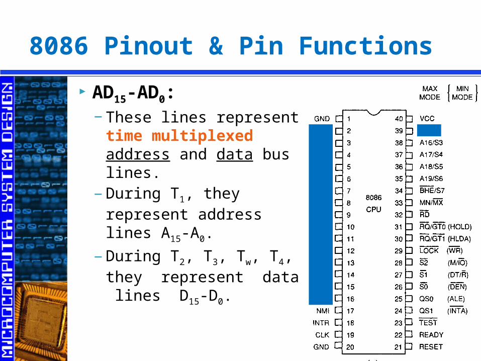
8086 Pinout & Pin Functions AD15-AD0:
−These lines represent time multiplexed address and data bus lines.
−During T1, they represent address lines A15-A0.
−During T2, T3, Tw, T4, they represent data lines D15-D0.

8086 Pinout & Pin Functions A19/S6-A16/S3:
−These lines represent time multiplexed address and status lines.
−During T1, they represent address lines A19-A16.
−During T2, T3, Tw, T4, they represent status signals S6-S3.

8086 Pinout & Pin Functions ALE (Address Latch Enable ):
−This signal is a HIGH pulse active during T1 of any bus cycle.
−It is provided by the processor to latch the address lines during T2, T3, Tw, T4 cycles.

8086 Pinout & Pin Functions READY:
−Active HIGH signal.−This is the acknowledgement
from the addressed memory or I/O device that it will complete the data transfer.
−If it is set LOW, the processor enters into wait states and remains idle.
−If it is set HIGH, it has no effect on the operation of the processor.

8086 Pinout & Pin Functions INTR (Interrupt Request):
−It is used to request a hardware interrupt.
−If it is held HIGH when IF = 1, the processor enters an interrupt acknowledge cycle after the current instruction complete execution.
INTA (Interrupt Acknowledge):−This signal is a response to the
INTR input pin. NMI (Non-Maskable Interrupt):
−Similar to INTR except that NMI does not check if the IF=1.
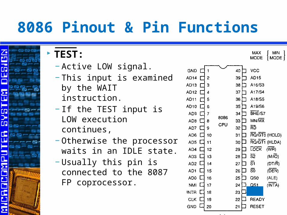
8086 Pinout & Pin Functions TEST:
−Active LOW signal.−This input is examined by the
WAIT instruction. −If the TEST input is LOW
execution continues,−Otherwise the processor waits
in an IDLE state.−Usually this pin is connected to
the 8087 FP coprocessor.
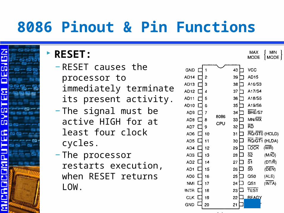
8086 Pinout & Pin Functions RESET:
−RESET causes the processor to immediately terminate its present activity.
−The signal must be active HIGH for at least four clock cycles.
−The processor restarts execution, when RESET returns LOW.
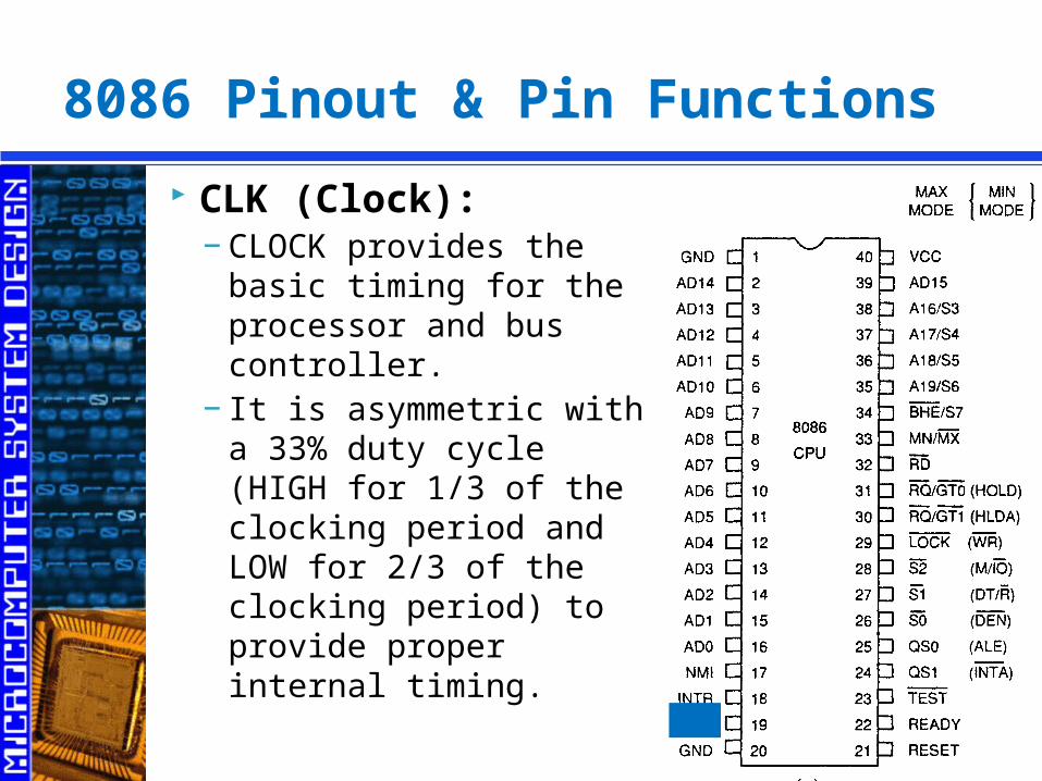
8086 Pinout & Pin Functions CLK (Clock):
−CLOCK provides the basic timing for the processor and bus controller.
−It is asymmetric with a 33% duty cycle (HIGH for 1/3 of the clocking period and LOW for 2/3 of the clocking period) to provide proper internal timing.
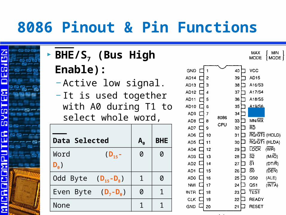
8086 Pinout & Pin Functions BHE/S7 (Bus High Enable):
−Active low signal.−It is used together with A0
during T1 to select whole word, odd byte, even byte or none.
Data Selected A0 BHE
Word (D15-D0) 0 0
Odd Byte (D15-D8) 1 0
Even Byte (D7-D0) 0 1
None 1 1
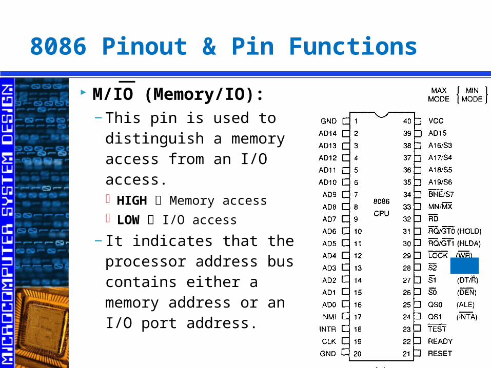
8086 Pinout & Pin Functions M/IO (Memory/IO):
−This pin is used to distinguish a memory access from an I/O access. HIGH Memory access LOW I/O access
−It indicates that the processor address bus contains either a memory address or an I/O port address.
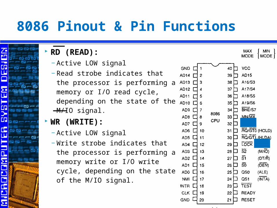
8086 Pinout & Pin Functions RD (READ):
−Active LOW signal−Read strobe indicates that the
processor is performing a memory or I/O read cycle, depending on the state of the M/IO signal.
WR (WRITE):−Active LOW signal−Write strobe indicates that the
processor is performing a memory write or I/O write cycle, depending on the state of the M/IO signal.

8086 Pinout & Pin Functions DT/R (Data
Transmit/Receive):−Needed in minimum system
that desires to use a data bus transceiver.
−It is used to control the direction of data flow through the transceiver.
−HIGH Transmit−LOW Receive

8086 Pinout & Pin Functions DEN(Data Enable):
−Active LOW signal−Needed in minimum system
that desires to use a data bus transceiver.
−It is used as an output enable for the transceiver.
−HIGH Enable−LOW Disable
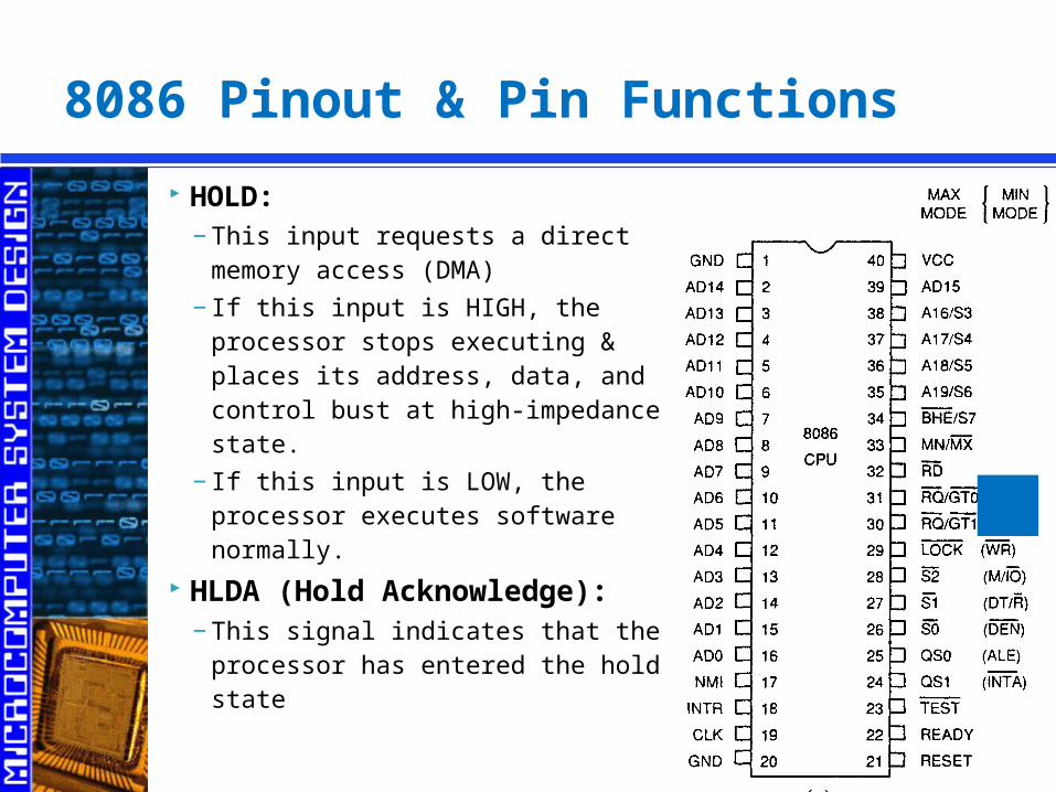
8086 Pinout & Pin Functions HOLD:
−This input requests a direct memory access (DMA)
−If this input is HIGH, the processor stops executing & places its address, data, and control bust at high-impedance state.
−If this input is LOW, the processor executes software normally.
HLDA (Hold Acknowledge):−This signal indicates that the
processor has entered the hold state

8086 Pinout & Pin Functions VCC (+5V Power Supply) GND (Ground) MN/MX
(Minimum/Maximum):−indicates what mode the
processor is to operate in.−HIGH minimum mode.−LOW maximum mode.

Minimum & Maximum Mode Operations
The 8086 can operate in either one of two modes of operation:−(1) Minimum Mode−(2) Maximum Mode
Minimum Mode: −The simplest and least expensive mode.−All the control signals for memory & I/O operations are
generated by the processor. Maximum Mode:
−Allows the system to use an external coprocessor such as 8087 (floating-point coprocessor) .
−Some of the control signals must be externally generated (requires an external bus controller 8288)

A very simple microcomputer system consists of the following part:
−(1) 8284A Clock Generator (15 MHz Crystal)
−(2) 8086 Microprocessor(Minimum Mode)
−(3) Bus System (Demultiplexed and Buffered)
−(4) Memory System (ROM & RAM Modules)
−(5) I/O System (Switches and LEDs)
Microcomputer System Design
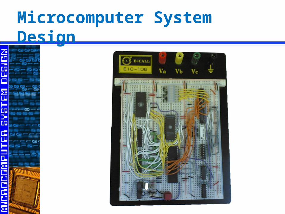
Microcomputer System Design

Basic Connections:
−GND: connect to 0V.
−VCC: connect to 5V.
−MN/MX’: connect to 5V (minimum mode).
−NMI & INTR: connect to 0V (no support for interrupts).
− CLK: connect to the CLK output of the clock generator.
−HOLD: connect to 0V (no direct memory access).
−TEST’: connect to 0V (no wait for co-processor).
−READY: connect to 5V (no wait cycles for slow devices).
−RESET: connect to RESET output of the clock generator.
Minimum Mode Connections

5V
5V
0V
0V5VRESET (8084A)
0V
0V
0V
0V(8284A) CLK
Related Documents


![MINIMUM 6 76.[45] HYUNDAI/KIA MINIMUM](https://static.cupdf.com/doc/110x72/61689563d394e9041f70d5f4/minimum-6-7645-hyundaikia-minimum.jpg)