Key Technologies and Research Development of CMOS Image Sensors

Welcome message from author
This document is posted to help you gain knowledge. Please leave a comment to let me know what you think about it! Share it to your friends and learn new things together.
Transcript

8/2/2019 Key Technologies and Research Development of CMOS Image Sensors _SEMINAR PPT
http://slidepdf.com/reader/full/key-technologies-and-research-development-of-cmos-image-sensors-seminar-ppt 1/19
Key Technologies and Research
Development of CMOS Image
Sensors

8/2/2019 Key Technologies and Research Development of CMOS Image Sensors _SEMINAR PPT
http://slidepdf.com/reader/full/key-technologies-and-research-development-of-cmos-image-sensors-seminar-ppt 2/19
INTRODUCTION
There are two types solid-state image sensor:
• CCD (Charge Coupled Device) SENSOR:A CCD Image sensor is ananalog device . When light strikes the chip it is held as a smallelectrical charge in each photo sensor . The charges are converted
to voltage one pixel at a time as they are read from the chip .Additional circuitry converts the voltage into digital form.
• CMOS(Complementary Metal Oxide Semiconductor) SENSOR :InCMOS sensor, each pixel has its own charge- to-voltage conversion ,
and the sensor often includes amplifiers , noise-correction , anddigitization circuits . These other functions on-chip increase thedesign complexity but reduce the space required for processing.

8/2/2019 Key Technologies and Research Development of CMOS Image Sensors _SEMINAR PPT
http://slidepdf.com/reader/full/key-technologies-and-research-development-of-cmos-image-sensors-seminar-ppt 3/19
CMOS IMAGE SENSOR(CIS)
The development of CMOS image sensor has experienced two
generations:
1.PPS (Passive pixel sensor) : These where the first image sensor devices
used in the 1960s.In passive pixel CMOS sensors , a photosite converts
photons into an electrical charge . This charge is then carried off the
sensor and amplified . The problem with these sensors is noise thatappears as a background pattern in the image . To cancel out this noise ,
sensors often use additional processing steps.
2.APS (Active Pixel Sensor):Image sensor elements with in-pixel
amplifiers are called ‘APS’ . Circuitry at each level determines what its
noise level is and cancels it out , thus reducing the noise associated with
each pixel .It is this active circuitry that gives the active pixel device its
name.

8/2/2019 Key Technologies and Research Development of CMOS Image Sensors _SEMINAR PPT
http://slidepdf.com/reader/full/key-technologies-and-research-development-of-cmos-image-sensors-seminar-ppt 4/19
ADVANTAGES OF CIS
• Wide dynamic range
• pixel size
•
read out speed• power consumption
• anti-radiation capability

8/2/2019 Key Technologies and Research Development of CMOS Image Sensors _SEMINAR PPT
http://slidepdf.com/reader/full/key-technologies-and-research-development-of-cmos-image-sensors-seminar-ppt 5/19
TWO KEY PROBLEMS OF AFFECTING IMAGE
QUALITY OF CMOS SENSOR
• Structure of CMOS Sensor
• Noise of CMOS Sensor
8/2/2019 Key Technologies and Research Development of CMOS Image Sensors _SEMINAR PPT
http://slidepdf.com/reader/full/key-technologies-and-research-development-of-cmos-image-sensors-seminar-ppt 6/19
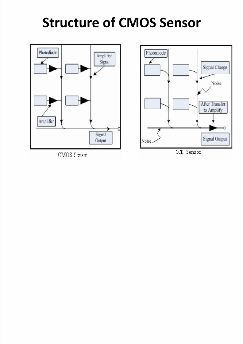
Structure of CMOS Sensor

8/2/2019 Key Technologies and Research Development of CMOS Image Sensors _SEMINAR PPT
http://slidepdf.com/reader/full/key-technologies-and-research-development-of-cmos-image-sensors-seminar-ppt 7/19
Noise of CMOS Sensor

8/2/2019 Key Technologies and Research Development of CMOS Image Sensors _SEMINAR PPT
http://slidepdf.com/reader/full/key-technologies-and-research-development-of-cmos-image-sensors-seminar-ppt 8/19
LATEST RESEARCH PROGRESS OF
CMOS IMAGE SENSOR
•
New Sensor-Exmor R CMOS
• Development of Noise Suppression for CMOS
Image Sensor

8/2/2019 Key Technologies and Research Development of CMOS Image Sensors _SEMINAR PPT
http://slidepdf.com/reader/full/key-technologies-and-research-development-of-cmos-image-sensors-seminar-ppt 9/19
New Sensor-Exmor R CMOS
Exmor is the new technologyimplemented by Sony in the
field of CMOS Image sensors .
This revolutionary new
technology performs on-chip
analog to digital conversion
and two-step noise reductionin parallel on each column of
CMOS sensor . The new
Exmor R CMOS sensor work
on “BACK ILLUMINATED
TECHNOLOGY” unlike
conventional sensors that
works on “FRONT
ILLUMINATED TECHNOLOGY”.

8/2/2019 Key Technologies and Research Development of CMOS Image Sensors _SEMINAR PPT
http://slidepdf.com/reader/full/key-technologies-and-research-development-of-cmos-image-sensors-seminar-ppt 10/19
Working of Exmor R CMOS sensor• In conventional sensors , the light receptors are placed behind the
wire circuits.(Front I Illuminated Technology).The wire circuits partlyblocks the light , while travelling to the receptive areas of sensor ,thus reducing the total amounts of light that reach to the lightreceptor.
•During low light conditions , the signals from the sensor have to beboosted electronically , creating the noise that’s seen as fuzzyimages or grains.
• The Exmor R CMOS sensor that works on back illuminatedtechnology which replaces the position of layers , so that lightreceptors are not blocked by wire circuits . Thus the light falls to
receptive areas of the of sensor and thus resulting in more light andthere is no need to boost the signals from sensor . This , in turnreduces the noise up to a great extent and hence results inimproved video and still picture quality with less light especially inlow light conditions.

8/2/2019 Key Technologies and Research Development of CMOS Image Sensors _SEMINAR PPT
http://slidepdf.com/reader/full/key-technologies-and-research-development-of-cmos-image-sensors-seminar-ppt 11/19

8/2/2019 Key Technologies and Research Development of CMOS Image Sensors _SEMINAR PPT
http://slidepdf.com/reader/full/key-technologies-and-research-development-of-cmos-image-sensors-seminar-ppt 12/19
Development of Noise Suppression
for CMOS Image Sensor
8/2/2019 Key Technologies and Research Development of CMOS Image Sensors _SEMINAR PPT
http://slidepdf.com/reader/full/key-technologies-and-research-development-of-cmos-image-sensors-seminar-ppt 13/19
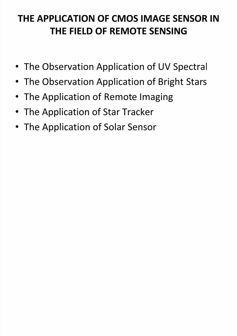
THE APPLICATION OF CMOS IMAGE SENSOR IN
THE FIELD OF REMOTE SENSING
• The Observation Application of UV Spectral
•The Observation Application of Bright Stars
• The Application of Remote Imaging
• The Application of Star Tracker
• The Application of Solar Sensor
8/2/2019 Key Technologies and Research Development of CMOS Image Sensors _SEMINAR PPT
http://slidepdf.com/reader/full/key-technologies-and-research-development-of-cmos-image-sensors-seminar-ppt 14/19
The Observation Application of UVSpectral
• CMOS image sensor uses standard production technique of CMOS semiconductor, the noise margin is big, anti-jamming
ability is very strong, spatial radiation protection ability is very
good, therefore CMOS image sensor can be used in the UV
spectral detector.

8/2/2019 Key Technologies and Research Development of CMOS Image Sensors _SEMINAR PPT
http://slidepdf.com/reader/full/key-technologies-and-research-development-of-cmos-image-sensors-seminar-ppt 15/19
The Observation Application of Bright
Stars
• When we use CCD imaging system to detect the bright star,
the pixel element is very easy saturated, this brings a series of
problem, such as blooming and smear and so on. If uses the
CMOS imaging system, which dynamic range is big, and it
does not have overflow between the pixel element, so wemay use CMOS imaging system to observe starry sky, which
includes the bright stars. Similarly, in other needs of the large
dynamic range of space applications, we also use the CMOS
imaging system.

8/2/2019 Key Technologies and Research Development of CMOS Image Sensors _SEMINAR PPT
http://slidepdf.com/reader/full/key-technologies-and-research-development-of-cmos-image-sensors-seminar-ppt 16/19
The Application of Remote Imaging
• At present, there are many earth observation imagingsystems, but the price of imaging system is very expensive,the power consumption is very high, the system size is veryhuge, it is difficult to achieve miniaturization. With thedecrease of spacecraft size, the light imaging technology will
become the main observation method, but the CCD imagesystem is difficulty to meet the requirements of volume,weight and the power consumption, however, the CMOSimage sensor has some advantages in power consumption,volume, weight, the cost, the radio resistance ability and so
on, therefore the CMOS image sensor has a widespreadapplication prospect in the field of remote imaging.

8/2/2019 Key Technologies and Research Development of CMOS Image Sensors _SEMINAR PPT
http://slidepdf.com/reader/full/key-technologies-and-research-development-of-cmos-image-sensors-seminar-ppt 17/19
The Application of Star Tracker
• With the development of spacecraft and the satellite technology, thestar tracker plays a vital role in navigation systems of spacecraft. Thestar tracker is mainly used for high accuracy posture determining of thesatellite, the airship, the aerospace craft, space station, it can be usedin rockets, missiles, guidance and control, but also can be use forprecise location and survey of the submarine, ships. Tradition star
tracker is based on CCD image sensor, because higher weight, powerconsumption and volume, the CCD image system is difficult to use inmicro-satellites.
• If we use the CMOS image sensor, these problems can be solved verywell, therefore under the premise of guaranteeing the image quality,CMOS image sensor can be used in star tracker.
•

8/2/2019 Key Technologies and Research Development of CMOS Image Sensors _SEMINAR PPT
http://slidepdf.com/reader/full/key-technologies-and-research-development-of-cmos-image-sensors-seminar-ppt 18/19
The Application of Solar Sensor
• The solar sensor is a widely used posture sensor, which has
strict requirements to the system weight, the system volume,
the system power consumption and so on, at the same time,
the rapid localization needs a fast readout speed. In view of
the technical advantages of CMOS sensor, it is impossible touse CMOS image sensor to replace CCD in solar sensor.

8/2/2019 Key Technologies and Research Development of CMOS Image Sensors _SEMINAR PPT
http://slidepdf.com/reader/full/key-technologies-and-research-development-of-cmos-image-sensors-seminar-ppt 19/19
THE END
THANK YOU
*NO QUESTIONS PLEASE
*DUE TO LACK OF KNOWLEDGE IN VLSI
Related Documents


