Panel (CD) (A29-1046-02) Knob (K29-7544-04) Knob (K29-7543-04) Front glass (B10-) Front glass (B10-3449-02) Front glass (B10-3471-03) Knob (K29-7541-02) Knob (K29-7541-02) Knob (K29-7545-04) Panel * (A60-) Front glass (B10-3448-02) Cassette lid (R) (A53-2122-02) Cassette lid (L) (A53-2121-02) Phone jack (E11-0280-05) Knob (K29-7553-01) MINI HiFi COMPONENT SYSTEM RXD-402/402E/402W/452/452E/452W/502/502E/ RXD-502W/552/552E/552W/572S/A41/A51 (XD-402~A51) ** SERVICE MANUAL © 1999-1/B51-5500-00 (K/K) 3590 Illustration is RXD-402. * Refer to parts list on page 48~. In compliance with Federal Regulations, following are reproduc- tions of labels on, or inside the product relating to laser product safety. **Refer to page 2 if you want to know system configuration. KENWOOD-Crop. certifies this equipment conforms to DHHS Regulations No. 21 DFR 1040. 10, Chapter 1, Subchapter J. DANGER : Laser radiation when open and interlock defeated. AVOID DIRECT EXPOSURE TO BEAM

Kenwood+Rxd452
Nov 08, 2014
Welcome message from author
This document is posted to help you gain knowledge. Please leave a comment to let me know what you think about it! Share it to your friends and learn new things together.
Transcript

Panel (CD)(A29-1046-02)
Knob(K29-7544-04)
Knob (K29-7543-04)
Front glass(B10-)
Front glass(B10-3449-02)
Front glass(B10-3471-03)
Knob(K29-7541-02)
Knob(K29-7541-02)
Knob(K29-7545-04)
Panel *(A60-)
Front glass(B10-3448-02)
Cassette lid (R)(A53-2122-02)
Cassette lid (L)(A53-2121-02)
Phone jack(E11-0280-05)
Knob(K29-7553-01)
MINI HiFi COMPONENT SYSTEM
RXD-402/402E/402W/452/452E/452W/502/502E/RXD-502W/552/552E/552W/572S/A41/A51
(XD-402~A51) **SERVICE MANUAL
© 1999-1/B51-5500-00 (K/K) 3590
Illustration is RXD-402.* Refer to parts list on page 48~.
In compliance with Federal Regulations, following are reproduc-tions of labels on, or inside the product relating to laser productsafety.
**Refer to page 2 if you want to know system configuration.
KENWOOD-Crop. certifies this equipment conforms to DHHSRegulations No. 21 DFR 1040. 10, Chapter 1, Subchapter J.
DANGER : Laser radiation when open and interlock defeated.AVOID DIRECT EXPOSURE TO BEAM
RXD-402(E) INT1P 99.6.9 7:25 PM y [ W 2

SYSTEM MAIN UNIT SPEAKER DESTINATION SYSTEM MAIN UNIT SPEAKER DESTINATION
XD-402 RXD-402 LS-N402 KPET XD-502 RXD-502 LS-N502 KPEXD-402E RXD-402E LS-N402 E1 XD-502E RXD-502E LS-N502 E1XD-402W RXD-402W LS-N402 Q XD-502W RXD-502W LS-N502 QXD-452 RXD-452 LS-N452 MXYTE XD-552 RXD-552 LS-N552 MXYTEXD-452E RXD-452E LS-N452 E1 XD-552E RXD-552E LS-N552 E1XD-452W RXD-452W LS-N452 Q XD-552W RXD-552W LS-N552 Q
XD-572S RXD-572S LS-N552 M1XD-A41 RXD-A41 LS-N452 KPXD-A51 RXD-A51 LS-N552 KP
VO
LU
ME
CD
TAPE
MU
TE
RC-5
52
REM
OTE C
ON
TR
OL U
NITEX
.BA
SS
TIM
E
INPU
T
BA
ND
PO
WE
R
TAPE
A/B
RA
ND
OM
REP
EAT
TEXT
DIS
P.
TUN
ING
6
12
3
45
6
78
9
0+1
0
32
¡1
4
7
MU
LTIC
ON
TRO
L
¢
DIS
C S
KIP
SO
UN
DCO
NTR
OL
MEN
UB
ACK
SEL
ECT
ENTE
R
VO
LU
ME
CD
TAPE
MU
TE
MEN
U
RC-5
52
ER
EM
OTE C
ON
TR
OL U
NITEX
.BA
SS
TIM
E
INPU
T
BA
ND
PTY
TA/N
EWS
RD
S D
ISP.
PO
WE
R
BA
CK
TAPE
A/B
RA
ND
OM
REP
EAT
TEXT
DIS
P.
TUN
ING
6
SET
ENTE
R12
3
45
6
78
9
0+1
0
32
¡1
4
7
MU
LTIC
ON
TRO
L
¢
DIS
C S
KIP
SO
UN
DCO
NTR
OL
FM indoor antenna (1) AM loop antenna (1)
Speaker cords (2)
Remote control (A70-1262-05): TEQE1...RC-552E
(A70-1253-05): KPMXYM1...RC-552
unit (1)
Remote control unit (1)
Use to adapt the plug on the power cord tothe shape of the wall outlet.(Accessory only for regions where use isnecesary.)
AC plug adaptor (1)
Provided in the speaker package
Batteries
(T90-0836-05) (T90-0837-05)
(E30-5535-05)
(E03-0115-05)
(R6/AA) (2)
RXD-402/452/502/552/572S/A41/A51
2
CONTENTS / ACCESSORIES / CAUTIONS
CONTENTS/ACCESSORIES/CAUTIONS...................2EXTERNAL VIEW/DISASSEMBLY FOR REPAIR.......3BLOCK DIAGRAM .......................................................4CIRCUIT DESCRIPTION .............................................5ADJUSTMENT .......................................................... 10WIRING DIAGRAM ....................................................14
PC BOARD ................................................................15SCHEMATIC DIAGRAM ............................................23EXPLODED VIEW .....................................................44PARTS LIST...............................................................48SPECIFICATIONS .....................................................59
Contents
Accessories
System configurationUnplug the power cord from the power outletthen, while holding the ENTER key depressed,plug the power cord again.
÷ Please note that resetting the microcomputer clearsthe contents stored in and returns and to conditionwhen it left the factory.
Operation to resetThe microcomputer may fall into malfunction (impos-sibility to operate, erroneous display, etc.) when thepower cord is unplugged while power is ON or due toan external factor. In this case, execute the followingprocedure to reset the microcomputer and return it tonormal condition.
ENTER(Main unit only)
Cautions
RXD-402(E) INT1P 99.6.9 7:25 PM y [ W 3

RXD-402/452/502/552/572S/A41/A51
3
EXTERNAL VIEW / DISASSEMBLY FOR REPAIR
EXTERNAL VIEW
DISASSEMBLY FOR REPAIR
BOTTOM SIDE
FRONT
HOW to open the tray if not comes out.
(1) Turn the friction arm counterclockwise using a screw driver and the like. (2) Pull out the tray front wards by hand when the tray comes just out.
Cover(F07-1655-02)
Slide switch(S62-0077-05)
Lock terminal board(E70-0053-05)
Lock terminal board(E70-0053-05)
Metallic cabinet(A01-3681-01)
Phono jack(E63-0116-05)
Lock terminal board(E20-0321-05)
Phono jack(E63-1037-05)
Oscillating module(W02-1114-05)
Illustration is RXD-402.
RXD-402(E) INT1P 99.6.9 7:25 PM y [ W 6

A PB
B R/P
B ERASE
BIASOSC CTRL
BIAS
VR5
HA12219NT
IC1
HA12136A
IC2
MPX
DPSS
IC4
HD74HC166P
FL DISPLAY
ED1
M66004SP
IC51
DRIVER
REMOCON
A1
D52TIMER
D51STANDBY
KEYMATRIX
ENHANCED ICFOR LED
IC52,53
JOG A JOG B VOL.
BU2090
+12VAVR
Q4
AVRQ6,7
-12V-12V
+12V
AVR
IC2+5VAVR
IC1+9V
RDS
CD +9V -B
GND
+B
+40VAVR
Q8
(X14- ) +5V
FL -35V
Q2
+5.6V AVRu-COM
FAST OFF
FL AC
AMP
forPOWER
AC IN
RF AMPCXA1571M
IC5
E-VOLTUNER
DECK
TUNERE-VOL
FL IC +5V
u-COMPULL UP
DRIVERTRACKING COIL
4ch BTL DRIVERBA5979S
DRIVERFOCUS COIL
DRIVERFEED MOTOR
DRIVERDISC MOTOR
IC6
AB
C
E
F
SWLD Q501
DSP.SERVO.CXD2587Q
IC7
DAC
CD +5V
CD +9V
(DSP,RF)
Q505
FM
DM
TA8409S(ROTARY TRAY)
TA8409S(LOADING)
LM
RM
IC8
IC9
M30622MA-173FPu-COM IC
IC1
IC2
K1
120V 240V
INP
UT
OU
TP
UT
MD
/DV
D
MD
RE
C J1
SURROUND 3BAND TONEEX-BASS
M62492FPSELECTOR,SURROUND,TON,E-VOL
RDSDEMODULATOR
IC3 (T,E,Q TYPE ONLY)
SAA6579T/RMODULETUNER ANT.
PHONESHEAD
POLARUNIT
-10dBATT
AMUTE
S1
OFF
ONON/OFFMATRIX
K1
RELAYSPEAKER
ch.OTHER
OUTSW
Lch
Rch
SPEAKER
MATRIXSPEAKER
BCLASS
ACLASS
Q1,2
Q3,4
B
A
REQ EQ
BIAS TRAP
PH A,B
MOTOR A
MOTOR B
MOTOR
SOL A,B
SPEEDTAPEA/B
MOTOR
SOL A,B
VR7,8LEVELB PB
LEVELVR1,2
A PB
PH A,B
B.CANCELBIASNOR
A-N/CA/BB1/2
DOLBYR/P DPSS
A,B CrCO2L RECR RECA,B PACKA,B PLAY
PSINCLK
PSLOAD
GRIDSEG
1635
CLKCS
DATA
KEY3KEY2KEY1
DATA1/2CLK
15LED
A JOG1/2 1/2
B JOG1/2ENC
+
+
+
+
+
+
RF.FE.TE
16.93MHZ
LOM+/-
ROM+/-
PHTR
TD/TUCL/OPPSW
MAIN10MHz
SUB32.768kHz
DATACLK MPX
TAPE REC
CLK
LATchDATA
MECHA.DECK
(X28- )
(X14- )
(X00- )
(X14- )
(X04- )
(X13- )MGC-E9001CD MECHA.
Q TYPE ONLY
2-710-22
X07-3030-21
ONLY
M TYPE ONLY
RXD-402/502
(X07- )
RXD-402/452/502/552/572S/A41/A51
4
BLO
CK
DIA
GR
AM
RXD-402(E) INT1P 99.6.9 7:25 PM y
[W 7

RXD-402/452/502/552/572S/A41/A51
5
CIRCUIT DESCRIPTION
1. Initialization
1-1 Setting of initial conditionsWhile pressing the [ENTER] key, put the plug into an ACpower outlet.
1-2 Initializing operation• A microcomputer is initialized for start when the AC
power is turned on when pressing the [ENTER] key. Atthat time, CD mechanism and CASSETTE mechanismare also initialized.
• During the initial operation,the display shows INITIALIZEand after that it will be returned to STANDBY condition.
1-3 Initial items and back up data
*BACKED UP DATA
1-4 Mechanism initialization
1-4-1 CD mechanism• Disc unclamps(traverse down).• Rotary tray rotates(1/3 rotation).• If a mechanism error occurs, CD ERR is indicated on the
display.
1-4-2 DECK mechanism• When initial condition becomes NG for the third time,
decide the error. The error condition is displayed as XERR on the display.
1-4-3 Error display• If both mechanism (CD/DECK) error occur, the display is
indicated as follows. CD & X ERR
2. Destination list of TUNER
ITEMS*POWER STANDBY*VOLUME 14*BALANCE CENTERMUTING OFFPROTECTION OFF
AMP S. DIRECT OFFDISPLAY MODE AUTO*AUTO POWER SAVE OFF*MD/DVD INPUT LEVEL -3*INPUT SEL. TUNER*BAND FM
TUNER *FREQUENCY LOWEST FREQUENCY*AUTO/MONO AUTO*P.CH --CH*CLOCK 0:00 (E/T/Q) 12:00 (OTHERS)
CLOCK *PROG. RECORDING ON/OFF TIME0:00 (E/T/Q) 12:00 (OTHERS)
*PROG. TIMER PLAY ON/OFF TIME 0:00 (E/T/Q)12:00 (OTHERS)
SLEEP TIMER OFFO.T.T. OFF*DIRECTION FORWARD
DECK *RVS MODE REVERSE*A/B B
KEYSELECTOR
FL INDICATIONMODE
• All the fluorescent display indicatorsand LEDs light on.
[BAND] TUNER • STANDBY and TIMER LEDs blink up.+ AC ON • The all illminated state is cleared by
pressing any main unit keys or remocon keys.
[INPUT] AUX • AUX TEST+ AC ON
Destinat-ion
Tunertype
BAND Receivingfrequency range
Channelspace IF RF
K,P K1
FM 87.5MHz~108.0MHz 100kHz +10.7MHz 25kHz AM 530kHz~1700kHz 10kHz +450kHz 10kHz
M,V,X,Y K2
FM 87.5MHz~108.0MHz 100kHz +10.7MHz 25kH AM 530kHz~1610kHz 10kHz +450kHz 10kHz
M K3
FM 87.5MHz~108.0MHz 100kHz +10.7MHz 25kHz MW 530kHz~1610kHz 10kHz +450kHz 10kHz SW 5.9MHz~17.9MHz 5kHz +450kHz 5kHz
M,V,X,Y E1 FM 87.5MHz~108.0MHz 50kHz +10.7MHz 25kHz AM 531kHz~1602kHz 9kHz +450kHz 9kHz
M E3
FM 87.5MHz~108.0MHz 50kHz +10.7MHz 25kHz MW 531kHz~1602kHz 9kHz +450kHz 9kHz SW 5.9MHz~17.9MHz 5kHz +450kHz 5kHz
E E1 FM 87.5MHz~108.0MHz 50kHz +10.7MHz 25kHzRDS AM 531kHz~1602kHz 9kHz +450kHz 9kHz
T E2
FM 87.5MHz~108.0MHz 50kHz +10.7MHz 25kHz
RDS MW 531kHz~1602kHz 9kHz +450kHz 9kHz LW 153kHz~279kHz 9kHz +450kHz 9kHz
Q Q
FML 65.0MHz~74.0MHz 10kHz +10.7MHz 5kHzFMH 87.5MHz~108.0MHz 50kHz +10.7MHz 5kHz MW 531kHz~1602kHz 9kHz +450kHz 9kHz LW 153kHz~279kHz 9kHz +450kHz 9kHz
AVdd
10
R107
k½
X13IC1
91pin(TYPE)
Destina- R107 Voltagetion [½] [V]
K 91k 4.51M1 39k 3.98M2 22k 3.44T 13k 2.83E 8.2k 2.25Q 4.7k 1.60
2-1 Discrimination of TUNER destination
3. Test mode3-1 Test mode of the receiver3-1-1 Setting of the test mode
While pressing the [INPUT] key or [BAND] key, put theplug into an AC power outlet.
3-1-2 Canceling of the test modeUnplug an AC power cord from an AC power outlet.
3-1-3 Condition in test mode• Power • • • • ON• EX.BASS • • • OFF• S.W • • • • • • • OFF• Selector mode or FL indication
RXD-402(E) INT1P 99.6.9 7:25 PM y [ W 10

RXD-402/452/502/552/572S/A41/A51
6
CIRCUIT DESCRIPTION3-1-4 Basic operation in test mode
(1) The muting during mode selection is not controlled inthe test mode.
(2) The test mode is cancelled when the AC power isturned off.
(3) The operation of the keys in the test mode as follows.
3-1-5 The operation of the keys in the test mode(1) DISPLAY /DEMO key
When this key is pressed in the test mode, all the flu-orescent display indicators and leds light off and nor-mal display are indicated cyclically.
(2) REV.MODE,DOLBY NR,A/B,REC/ARM keysThe volume level settings can be made as follows.REV.MODE • • • volume min+1stepDOLBY • • • • • • volume 14 *RXD-402(TAPE E.Q.)A/B • • • • • • • • • volume20REC/ARM • • • • volume max (50)
(3) DISC SKIP keyWith the selector on TUNER, the S level indicationchanges cyclically as follows by pressing the [DISCSKIP] key.1 ATT is switched off. "ATT off & TUNER S levelXX"2 ATT is switched on. "ATT on & TUNER S levelXX"3 ATT is switched off. Normal display.
XX means A/D value(HEX) of S.(4) DECK STOP key
With the selector on TUNER, when the [DECK STOP]key operated, the preset memory can be changed as10 steps.
(5) FWD PLAY/RVS keyWith the selector on TUNER, the P. CALL is operatedby pressing the [ FWD PLAY] and [ RVS PLAY] keys.FWD PLAY key • • • • P. CALL upRVS PLAY key • • • • P. CALL down
(6) CD OPEN /CLOSE keyWith the selector on TUNER, the channel space set-tings can be made cyclically by pressing the [CDOPEN/CLOSE] key with M version.
(7) DECK STOP keyWith the selector on AUX, when the [DECK STOP ]key operated,the S. direct (ON/OFF) can be changed.
(8) DISC 1 keyWith the selector on something other than TUNER,whenever the [DISC1] key is pressed, the setting ofE.Q changes cyclically as follows.
(9) DISC 2 keyWith the selector on AUX, MD/DVD input level can bemade cyclically by pressing the [DISC 2] key .
INITIALIZED VALUE íî LEVEL MAX
(10) DISC 3 keyWith the selector on AUX, the balance level settingcan be made cyclically by pressing the [DISC 3] key .
(11) DISC SKIP keyWith the selector on something other than TUNER,the muting (ON/OFF) can be changed.
3-2 Test mode of cassette deck3-2-1 Setting of the test mode
While pressing the [deck play] key, put the plug into anAC power outlet.
3-2-2 Canceling of the test modeUnplug an AC power cord from an AC power outlet.
3-2-3 Condition in test mode(1) Initial condition• DOLBY-0FF• AUDIO-MUTE OFF
(2) Mechanism SW detection
(3) 4-sec recordingIf the REC key is pressed, the system record for 4sec. Then, it rewinds to the recording starting positionand plays back automatically.If the REC key is pressed, during the 4-sec recordingoperation, the system records further for 4-sec, thenreturn to the starting position of the first 4-sec record-ing operation and plays back.
3-3 Test mode of CD player3-3-1 Setting of the test mode
While the pressing the [PLAY/PAUSE] key, put the pluginto an AC power outlet.
3-3-2 Canceling the test modePress the stop key on stop mode or unplug the AC cordfrom an AC power outlet.
3-3-3 The operation of the keys in the test mode.
DISPLAYA pack SW E.QA -CRO2 PROG.12B-FWD O.T.TB pack SW AUTOB-CRO2 STB-RVS ANTENNA
10 20 30 40 00( )
E.Q MAX E.Q MIN E.Q FLAT
Lch MAX Rch MAX CENTER
KEY DISPLAY OPERATION
PLAY/PAUSE+AC IN CD TEST
• Setting of the test mode. • Tray 1/3 rotation. • Tray opens automatically.
STOP 0 • Tray closes. • Change or cancel the test mode.
PLAY/PAUSE 03 --:--05**:**
• Tray closes/disc clamps. • T-servo off(03) or on (05).
DOWN FINISH • Tray 1/3 rotation.
DISC3
07 EF/FB08 TG/FG09 TE/RF10 TE/VC
• Mechanism stops when theautomatic adjustment is finished.
• Display changes cyclically. • If NG, display blinks up.
DISC2 216**:** • Tray closes. • Disc2 clamps. • Plays track 16.
DISC1 • Tray closes/disc clamps. • Plays track 32.
RXD-402(E) INT1P 99.6.9 7:25 PM y [ W 11

RXD-402/452/502/552/572S/A41/A51
7
CIRCUIT DESCRIPTION
4. Main microprocessor
4-1 Microprocessor periphery block diagram
4-2 Key matrix
SERIES
EXPANDER
X14, IC51
X14, IC52, 53
X04, IC7
X04, IC3
TUNER PACK IC2
X28, IC4
X04, IC2
X28, IC1
X13, IC1
RXD-402(E) INT1P 99.6.9 7:25 PM y [ W 14

RXD-402/452/502/552/572S/A41/A51
8
CIRCUIT DESCRIPTION
Pin No. Name I/O Description Active1 S.LEVEL I RDS S level input.2 PLL DO I PLL IC data input.3 SD I SD detector input.4 ST I Stereo detector input.5 PLL CE O PLL IC chip enable.6 RDS DATA I RDS data input.7 PLL CLK O PLL IC clock output.8 BYTE I Ground.9 CNVSS - Ground.10 XCIN I Timer clock input(32.768kHz).11 XCOUT O Timer clock output(32.768kHz).12 RST I u-com reset signal input. H : normal L : reset13 XOUT O Main clock output(10MHz).14 VSS - Ground.15 XIN I Main clock input(10MHz).16 VCC(BU) - No used (+5v).17 HMI - u-com power supply(+5v).18 REM I Remocon signal input. H : normal L : reset19 RDS CLK I RDS clock input.20 SCOR I Sub code synchronism signal input.21 NC - No connection.22 CLSW I CD load switch (SW3) input port of CD mechanism.23 OPEN SW I CD unload switch (SW3) input port of CD mechanism.24 RTL O Rotary motor opposite direction (CCW) output.25 BRKM O Rotary motor brake control. H : normal L brake26 CLOSE O Load motor opposite direction (taking out) output.27 OPEN O Load motor positive direction (dragging out) output.28 SQCK O CD sub code clock output.29 SQSO I CD sub code input.30 NC - No connection.31 FL DATA O FL driver data output.32 CE I Power failure signal input. H : AC on L : AC off33 FLCLK O FL driver clock output.34 FLCS O FL driver strobe output.35 RTR O Rotary motor positive direction (CW) output.36 TDSW I Traverse down switch (SW1) input port of CD mechanism. H : off L : on37 TUSW I Traverse up switch (SW1) input port of CD mechanism. H : off L : on38 PHTR I CD photo transistor (Q1) detector input.
39 PSSW I Tray position & disc detector switch (SW2) input port ofCD mechanism.
40 XRST O CD DSP IC reset control.41 CD MUTE - No connection.42 DC OFF O CD DSP IC power control. H : on L : off43 MON O Spindle motor (ON/0FF) changeover. H : on L : off44 LDC O Laser ON/OFF signal output. H : off L : on45 SCLK O CD sense data read out clock output.46 SENS I CD sense input.47 CLOK O CD DSP IC clock.48 XLAT O CD DSP IC latch.49 DATA O Data output to DSP IC.50 EVCLK O Clock output to E. vol(IC2).51 EVLAT O Latch output to E. vol(IC2).52 EVDATA O Data output to E. vol(IC2).53 A-JOG1 I Jog A (S28) input.
4-3 Pin description of microprocessor: M30622MA-173FP (X13, IC1)
RXD-402(E) INT1P 99.6.9 7:25 PM y [ W 15

RXD-402/452/502/552/572S/A41/A51
9
CIRCUIT DESCRIPTIONPin No. Name I/O Description Active
54 A-JOG2 I Jog A (S28) input.55 B-JOG1 I Jog B (S29) input.56 B-JOG2 I Jog B (S29) input.
57,58 ENC1,2 I Rotary encoder(S27) input.59 LEDCLK O Clock output to LED controller(IC52,53).
60,61 LEDDT1,2 O Data output to LED controller(IC52,53).62 VCC(BU) - u-com power supply(+5v).63 LMUTE O Deck line mute control.64 VSS - Ground.65 B-PH I B deck reel sensor input.66 A-B2 O Deck A/B changeover control 1.67 A-B1 O Deck A/B changeover control 2.68 A120/70 O Play back equalizer control. H :70u L :120u69 B1/2 O Muting control for recording.70 D-R/P O Dolby recording/play back control. H : recording L : playback 71 DOLBY O Dolby B ON/OFF changeover. H : on L : off72 R/P O Deck recording /play back control. H : recording L : playback 73 NOR O NORMAL/CRO2 changeover.74 BIAS O Deck bias control output. H : on L : off75 BEAT.C O Deck beat cancel control output. H : on L : off76 B.SOL O Deck solenoid control output. H : on L : off77 CPM O Deck motor control output. H : on L : off78 A.SOL 0 Deck solenoid control output. H : on L : off79 CLK O Clock output to bias control IC(X28,IC4).80 PSLOAD O Parallel serial IC load. H : shift L : load81 AMUTE 0 Audio muting control. H : off L : on82 ATT O E. volume attenuation output. H : off L : on83 POWER O Power relay control. H : on L : off84 PROTECT I Protection detection input. H : protection on L : off 85 SP.RELAY O Speaker relay control output. H : on L : off86 LED(STBY) O LED(STANDBY) control output. H : on L : off87 LED(TIMER) O LED(TIMER) control output. H : on L : off88 PSIN I Parallel serial IC input data.89 SPEANA I Music signal input port.90 MODEL I Model discrimination input. H :XD-502 L :XD-40291 TYPE I Discrimination port of tuner destination.92 DPSS I Deck DPSS detection input.93 A-PH I A deck reel sensor input.
94,95 KEY3,2 I A/D key input (key3,2).96 AVSS - A/D ground.97 KEY1 I A/D key input (key1).98 VREF - A/D reference voltage.99 AVCC(BU) - Analog power supply(+5V).100 PLL DATA I PLL IC data input.
5. IC controller
5-1 RDS LED driverPin No. Name I/O Description
1 VSS - GND2 DATA I DATA INPUT3 CLOCK I CLOCK INPUT4 PTY O PTY ON/OFF LED5 NC O NO USED6 EON O EON INT LED7 NC O NO USED
Pin No. Name I/O Description8 TA O TA ON/OFF LED9 TP O TP ON/OFF LED10 RDS O RDS ON/OFF LED
11~13 NC O NO USED14 NEWS O NEWS ON/OFF LED15 NC O NO USED16 VDD - +5V POWER SUPPLY
RXD-402(E) INT1P 99.6.9 7:25 PM y [ W 18

RXD-402/452/502/552/572S/A41/A51
10
ADJUSTMENT
No. ITEMINPUT
SETTINGSOUTPUT
SETTINGSAMPLIFIERSETTINGS
ALIGNMENTPOINTS
ALIGN FOR FIG.
Unless otherwise specified, the individual switches should be set as following : POWER : ON SELECTOR : CD
1 IDLE CURRENT –
Connect a DCvoltmeter toCN3 (Lch),CN4 (Rch)X07, A/2.
VOLUME : 0VR1 (L)VR2 (R)X07, A/2
6 mV (a)
Dc voltmeter
6 mV
CN3 (L)CN4 (R)
(a)
Amp adjustment
RXD-402(E) INT1P 99.6.9 7:26 PM y [ W 19

RXD-402/452/502/552/572S/A41/A51
11
ADJUSTMENT
X04-1313 Q TYPE (65MHz~74MHz BAND)
N0. ITEM INPUTSETTINGS
OUTPUTSETTINGS
TUNERSETTINGS
ALIGNMENTPOINTS ALIGN FOR FIG.
1 VCO
(C)69 MHz,
70 dBf (ANT INPUT)1 kHz, 0 kHz DEVSUB, 0 kHz DEV
Connect a frequencycounter to VCO monitor
X04 (CN2).
AUTO69 MHz VR 2
Adjust it thefrequency counterreads 31.25 kHz
±100 Hz.
(a)
2 RESONANCEPOINT
(C)69 MHz,
70 dBf (ANT INPUT)1 kHz, 40 kHz DEVSUB, 10 kHz DEV
Select : L or R
Connect a oscilloscopeto TUNER OUT(CN6).
AUTO69 MHz TC 1 Minimum
crosstalk. (a)
3 SEPARATION (C)SAME AS ABOVE
Connect a oscilloscopeto TUNER OUT(CN6).
AUTO69 MHz VR 1 Minimum
crosstalk. (a)
(A)
(B)
(C)
(D) AM-SG
FM-MPX-SG
FM-MPX-SG
TO CN63pin (Lch)1pin (Rch)2pin (GND)
POLAR SG
AC voltmeter Oscilloscope
Distortion meterDummy antenna
Fig (a)
Tuner adjustment
RXD-402(E) INT1P 99.6.9 7:26 PM y [ W 22

X13 FOIL SIDE VIEW
VR1
FE. B
RF FE1 FE2 TE2 TE1 VC
RXD-402/452/502/552/572S/A41/A51
12
ADJUSTMENT
(d)
(a) Laser Power (b) Test point
Pickup
0.05~0.15 mW
Optical power meter
RF signal in test mode (PLAY).Perform the tangential and focusing offset are focusedinto one point on the display. The crossing points aboveand below the center shall also be looked clearly.
No.
1
2
ITEM
LASERPOWER
FOCUSERROR
BIAS
INPUTSETTING
–
Test discType 4
OUTPUTSETTING
Connect an oscillo-scope as follows.
CH1 : RFCH2 : FE1GND : VC
Set the senor sectionof the optical powermeter on the pickup
lens.
PLAYERSETTING
Press the"PLAY"keyto check that the dis-
play is "03".
Press the "PLAY"key. Confirm that the
display is”05”
ALIGNMENTPOINT
FEBIAS VR1
–
ALIGN FOR
On the powerfrom.0.05 to 0.15mw.when the diffractiongrating is correctlyaligned with the RFlevel of 0.8Vp-p or
more
Optimum eye pattern(DC=±330mV)
FIG.
(a)
(b)(d)
Note:Type 4disc :SONY YEDS-18 Test Disc or equivalent. (KTD-02)LPF : Around 47k½ + 390pF or so.
CD player adjustment
Step 1,2 are in TEST MODETEST MODE : While pressing the [CD PALY] key, plug the AC power cord into the AC power wall outlet.
RF signal FAC coupled
RXD-402(E) INT1P 99.6.9 7:26 PM y [ W 23

RXD-402/452/502/552/572S/A41/A51
13
ADJUSTMENT
No
q1 r
q2 r
q1 r
q1 r
q2 r
ITEM
Demagnetizationand cleaning
Azimuth of theREC/PLAY head
TAPESPEED(NORMAL)
PLAYBACKLEVEL
BIAS CURRENT
INPUTSETTING
\
TCC-153MTT-114
10kHz, - 10dB
TCC-110MTT-111
SCC-17273kHz
(A)Adjust the AG
for the output ofthe DECK to
become1kHz(-30dBs)/10kHz(-30dBs).
MTT-256U,TCC-160
315Hz, 0dB
Adjust the playbackoutput to -6.0dBs
OUTPUTSETTING
\
iB j
iB j
iB j
iB j
DECKSETTING
Demagnetization:POWER OFF
Cleaning: PLAY
PLAY
PLAY
PLAY
Adjust the REC VRlevel so that the line
out is -2.6dBs at1kHz, and record
and playback1kHz/10kHz alter-
nately.
ALIGNMENTPOINT
Recordinghead, erasehead,capstan
pinch roller
FWD RVS
A/B DECK VR 5
A DECKVR 1 (L)VR 2 (R)
B DECKVR 7 (L)VR 8 (R)
VR 3 (L)VR 4 (R)
ALIGN FOR
Demagnetize theREC / PLAY head
with the head eras-er.Clean the REC /PLAY head, erasehead,capstan andpinch roller using acotton swab slightly
damped with alcohol.
Adjust the output tomaximum and adjustthe azimuth adjust-ment screw for the
Lissajours waveformpattern of the oscillo-
scope to becomeclose to a 45°straight line.
Adjust the tapespeed so that 3kHzis obtained at thecenter of the tape.
Record 1kHz and10kHz alternately,and adjust the biascurrent adjustment
potentiometer for theplayback levels tobecome the same.
FIG.
Unless otherwise specified, set the respective switches as follows: 0dBs=0.775V TAPE : NORMAL DOLBY : OFF PLAY OUT : Lch (X28,CN6 @pin), Rch (X28,CN6 Cpin)
ø. Cassette mechanism unit (Adjustment of the REC / PLAY head)
¿. PC BOARD ADJUSTMENT
¡. PC BOARD ADJUSTMENT
Cassette Deck adjustment
{
(A) (B)
X28, CN6
L IN
L OUT
R OUT
R IN
GND
1
5
AC voltmeter AG Oscilloscope AC voltmeter
Frequency counter
RXD-402(E) INT1P 99.6.9 7:26 PM y [ W 26

RXD-402/452/502/552/572S/A41/A51
14
CN1 CN2
WH2E2CN1
CN1WH3 E3
CN5 CN4
CN1
E1
WH1
E2WH1
E1
J4
S1
SURROUNDSW
Rch
Lch
SU
RR
OU
ND
SP
EA
KE
RS
GND J2
AM ANT
FM75
J1
MD REC OUTPUT
MD/DVD INPUT
A501 DIGITAL OUT
E1WH3
E2
CN2 WH4
WH1
WH2
CN1
CN3 CN2
CN5 CN1
RXD-502E (X28-2980-10)
RXD-502W (X28-2983-81)
DESTINATION
RUSSIACOUNTRY
Q 3-81
UNIT No.ABB.
DESTINATION
EUROPECOUNTRY
E1 0-10
UNIT No.ABB.
ABB.COUNTRY
ABB.COUNTRY
EUROPE
U.S.ACANADA
EPK
0-10
DESTINATION
RXD-502 (X28-2980-10)
RUSSIA
UNIT No.
Q 3-82
DESTINATION
RXD-402W (X28-2983-82)
EUROPE
UNIT No.
E1 0-11
DESTINATION
RXD-402E (X28-2980-11)
COUNTRY
U,K
UNIT No.ABB.
T
RXD-452W (X28-2983-82)
RXD-572S (X28-2980-10)
RXD-552W (X28-2983-81)
RXD-402 (X28-2980-11)
DESTINATION
CANADAU.S.A
EUROPE
COUNTRY
PK
E0-11
UNIT No.ABB.
DESTINATION
RUSSIACOUNTRY
Q 3-81
UNIT No.ABB.
RXD-552E (X28-2980-10)
DESTINATION
EUROPECOUNTRY
E1 0-10
UNIT No.ABB.
DESTINATION
GENERAL MARKETCOUNTRY
M1 0-10
UNIT No.ABB.
MGENERAL MARKET
EUROPE
AUSTRALIAU,K
ETX 0-10
DESTINATION
RXD-552 (X28-2980-10)
PXCOUNTRY UNIT No.
YABB.
RXD-A51 (X28-2980-10)
DESTINATION
U.S.ACANADA
COUNTRYKP
0-10
UNIT No.ABB.
DESTINATION
RUSSIACOUNTRY
Q 3-82
UNIT No.ABB.
RXD-A41 (X28-2980-11)
XAUSTRALIA
RXD-452E (X28-2980-11)
DESTINATION
EUROPECOUNTRY
E1 0-11
UNIT No.ABB.
JAPANEUROPE
U,K
JET
0-11
GENERAL MARKET
DESTINATION
RXD-452 (X28-2980-11)
COUNTRYPX
ABB.YM
UNIT No.
DESTINATION
U.S.ACANADA
COUNTRYKP
0-11
UNIT No.ABB.
RXD-502W (X13-7613-81)
ABB.RUSSIA
COUNTRYDESTINATION
3-81Q
UNIT No.
E1ABB.
EUROPE
DESTINATIONCOUNTRY
2-71
UNIT No.
KU.S.A.
RXD-502E (X13-7612-71)
CANADAEUROPE
PE 2-71
0-10
ABB.
RXD-502 (X13-761X-XX)
COUNTRYDESTINATION
UNIT No.
ABB.
RXD-402W (X13-7613-81)
DESTINATIONCOUNTRYRUSSIA
UNIT No.
3-81Q
RXD-402E (X13-7612-71)
ABB.E1
COUNTRYEUROPE
DESTINATIONUNIT No.
2-71
U.K.EUROPE
CANADAU.S.A.
0-51T2-71E
0-10PK
ABB.
RXD-402 (X13-761X-XX)
COUNTRYDESTINATION
UNIT No.
ABB.COUNTRY
GENERAL MARKET M 0-21
RXD-572S (X13-7610-22)
ABB.DESTINATIONCOUNTRY
GENERAL MARKET M1
UNIT No.
0-22
ABB.
RXD-552W (X13-7613-81)
COUNTRYRUSSIA
DESTINATIONUNIT No.
3-81Q
RXD-552E (X13-7612-71)
E1ABB.COUNTRY
EUROPE
DESTINATION
2-71
UNIT No.
EUROPE
AUSTRALIAU.K.
E 2-71
XT 0-51
DESTINATION
RXD-552 (X13-761X-XX)
ABB.COUNTRYPX
DESTINATION
Y
UNIT No.
ABB.
CANADA
COUNTRYU.S.A.
0-10P
UNIT No.
K
UNIT No.
RXD-A51 (X13-7610-10)
ABB.COUNTRYRUSSIA 3-81Q
E1
RXD-452W (X13-7613-81)
DESTINATION
EUROPE 2-71
RXD-A41 (X13-7610-10)
0-01JJAPAN
RXD-452E (X13-7612-71)
DESTINATION
EUROPE
UNIT No.
2-71E
GENERAL MARKETAUSTRALIA
U.K.
PX0-21M
0-51TX
Y
RXD-452 (X13-761X-XX)
ABB.DESTINATIONCOUNTRY UNIT No.
ABB.COUNTRY
CANADAU.S.A.
DESTINATION
PK
0-10
UNIT No.
COUNTRY ABB.
COUNTRY ABB.
QABB.
RXD-552W (X07-3030-21)
E1
RUSSIACOUNTRYDESTINATION
EUROPE
0-21
UNIT No.
0-21
RXD-552E (X07-3030-21)
YM
ETX
DESTINATION
EUROPE
AUSTRALIAU.K.
GENERAL MARKETPX
UNIT No.
0-21
RXD-552 (X07-3030-21)
PK
ABB.
RXD-A51 (X07-3030-10)
DESTINATION
CANADAU.S.A.
COUNTRYDESTINATION
0-10
UNIT No.
UNIT No.
RXD-452W (X07-3030-11)
QABB.
E1
RUSSIA
DESTINATIONCOUNTRY
EUROPE
0-11
UNIT No.
0-11ABB.
RXD-452E (X07-3030-11)
J
MX
TE
JAPAN
COUNTRYDESTINATION
EUROPEU.K.
AUSTRALIAGENERAL MARKET
UNIT No.
0-22
0-11
ABB.
RXD-452 (X07-303X-XX)
Y
PK
ABB.
DESTINATIONCOUNTRY
PX
U.S.A.CANADA
COUNTRYDESTINATION
UNIT No.
0-11
UNIT No.
RXD-A41 (X07-3030-11)
COUNTRY ABB.
RXD-502W (X07-3030-21)
RUSSIA
DESTINATIONCOUNTRY
0-21Q
UNIT No.ABB.
EUROPE 0-21E1
DESTINATION
EEUROPE 0-21
RXD-502E (X07-3030-21)
DESTINATIONUNIT No.
CANADA
COUNTRYU.S.A.
0-10P
UNIT No.
KABB.
RXD-502 (X07-303X-XX)
RUSSIA 0-11Q
RXD-402W (X07-3030-11)
DESTINATIONCOUNTRY UNIT No.ABB.
RXD-402E (X07-3030-11)
COUNTRYEUROPE
DESTINATIONABB.
0-11E1
UNIT No.
EUROPEU.K.
CANADA
E
0-11TP
RXD-402 (X07-3030-11)
DESTINATION
U.S.A.COUNTRY
UNIT No.
KABB.
GENERAL MARKET
DESTINATIONCOUNTRY
0-21M1
UNIT No.ABB.
RXD-572S (X07-3030-21)
RXD-552 (X00-293X-XX)
YM
ABB.
XTEEUROPE
AUSTRALIAU.K.
COUNTRY
GEMERAL MARKETPX
DESTINATION
2-71
0-21
UNIT No.
KP
ABB.
RXD-A51 (X00-2930-10)
Q
CANADAU.S.A.
COUNTRYDESTINATION
RUSSIA
0-10
UNIT No.
2-72
UNIT No.
RXD-452E (X00-2932-72)
ABB.
RXD-452W (X00-2932-72)
ABB.E1
DESTINATIONCOUNTRY
COUNTRYEUROPE
DESTINATION
UNIT No.
2-72
UNIT No.
JETX
YM
ABB.
JAPANEUROPE
GEMERAL MARKETAUSTRALIA
U.K.
COUNTRYPX
0-01
2-72
0-22
RXD-452 (X00-293X-XX)
RXD-A41 (X00-2930-11)
PK
ABB.
DESTINATION
CANADA
DESTINATION
U.S.A.COUNTRY
0-11
UNIT No.
COUNTRY ABB.RUSSIA 2-72Q
RXD-402W (X00-2932-72)
DESTINATIONUNIT No.
RXD-402E (X00-2932-72)
COUNTRYEUROPE
DESTINATIONUNIT No.
2-72ABB.E1
UNIT No.
KU.S.A.
EUROPEU.K.
CANADA
2-72E
0-11
TP
RXD-402 (X00-293X-XX)
DESTINATIONCOUNTRY
UNIT No.ABB.
RXD-572S (X00-2930-21)
GEMERAL MARKET
DESTINATIONCOUNTRY
0-21M1
UNIT No.ABB.
COUNTRYRUSSIA 2-71Q
ABB.
2-71E1EUROPE
RXD-552W (X00-2932-71)
DESTINATION
RXD-552E (X00-2932-71)
DESTINATIONCOUNTRY
UNIT No.ABB.
RXD-502E (X00-2932-71)
DESTINATION
RXD-502W (X00-2932-71)
DESTINATION
RUSSIACOUNTRY
COUNTRYEUROPE
Q 2-71
UNIT No.ABB.
ABB.E1 2-71
UNIT No.
RXD-502 (X00-293X-XX)
DESTINATION
EUROPECANADA
COUNTRYU.S.A.
0-10
EP
2-71
UNIT No.
KABB.
S2
S1
RXD-502 (X14-493X-XX)
RXD-502E (X14-4932-71)
RXD-502W (X14-4932-71)
RXD-402E (X14-4932-72)
E1EUROPE
QRUSSIA
DESTINATIONCOUNTRY ABB.
DESTINATIONCOUNTRY ABB.
EUROPE ECANADA
COUNTRYU.S.A
P
ABB.K
DESTINATION
DESTINATIONCOUNTRYEUROPE
ABB.E1
2-71
2-71
UNIT No.
UNIT No.
2-71
UNIT No.
0-10
2-72
UNIT No.
RXD-402W (X14-4932-72)
RXD-402 (X14-493X-XX)
RXD-552E (X14-4932-71)
RXD-A51 (X14-4930-10)
RXD-552 (X14-493X-XX)
RXD-552W (X14-4932-71)
RXD-572S (X14-4930-10)
DESTINATION
RUSSIACOUNTRY
QABB.
U,KEUROPECANADA
TEP
DESTINATION
U.S.ACOUNTRY
KABB.
E1EUROPE
DESTINATIONCOUNTRY ABB.
QRUSSIA
DESTINATIONCOUNTRY ABB.
GENERAL MARKET M1
GENERAL MARKET
EUROPE E
AUSTRALIAU,K
XT
M
DESTINATION
PXCOUNTRY
YABB.
DESTINATIONCOUNTRY ABB.
CANADA P
DESTINATION
U.S.ACOUNTRY
KABB.
2-72
UNIT No.
0-11
2-72
UNIT No.
2-71
UNIT No.
2-71
UNIT No.
0-10
2-71
0-10
UNIT No.
0-10
UNIT No.
UNIT No.
RXD-452E (X14-4932-72)
RXD-452W (X14-4932-72)
RXD-A41 (X14-4930-11)
RXD-452 (X14-493X-XX)
QRUSSIA
DESTINATIONCOUNTRYEUROPE
ABB.E1
DESTINATIONCOUNTRY ABB.
EUROPE E
ABB.COUNTRY
GENERAL MARKETAUSTRALIA
U,KJAPAN
T
XJ
PX YM
DESTINATION
CANADAU.S.A
PK
DESTINATIONCOUNTRY ABB.
2-72
2-72
2-72
UNIT No.
UNIT No.
0-11
UNIT No.
0-11
UNIT No.
WH4
WH3
WH1
WH2
CN3
A
Rch 4
Lch 3
Rch 2
Lch 1
(OPTICAL)
J3 PRE OUTS.W
Rch 2
Lch 1
J2 SPEAKERSFRONT
A
NO
A
NO
A
NO
A
YES
A
YES
YES
A
A
NO
A
YES
YES
A
YES
YES
A
NO
A
NO
A
NO
A
YES
NO
A
NO
A
E1
33 33
1 1
12
1
12
1
11
11
1
1
21 21
1 1
1 12
1 12
1
4
1
4
ON
OFF
15 15
1 1
3
1
3
1
1
5
2 1
2
1
1
15
3
5
1
2
1
20
1
20
1
1
33 33
1
F2
T1
220-240V
110-120V
1
4
1
4
10 10
1 1
10
1
10
1
11
4 4
17
1
17
1
(K,P)(Y,M,M1)
(Q)(X)
(T,E,E1)
: AC120V 60Hz: AC110-120V/220-240V~
50/60Hz: AC220V~ 50Hz: AC240V~ 50Hz: AC230V~ 50Hz
(J) : AC100V 50/60Hz
F1
F1
2
4
5
(X13-761X-XX)
(X07-303X-XX) (A/2)
(X07- ) (B/2)
(X00-293X-XX) (A/3)
(X28-298X-XX) (D40-1618-05)
(X04-1313-84)
CD MECHANISM
MPX UNIT
USED (Q) TYPE
MECHANISMCASSETTE
SURROUND UNITMATRIX
(X00- ) (B/3)
(X00- ) (C/3)PRIMARY UNIT
SECONDARY UNIT
PRIMARY UNIT(X00- ) (C/3)
USED (M,M1,Y) TYPE
USED EXCEPT (M,M1,Y) TYPE
POWER SUPPLY UNIT
(M,M1,Y) TYPEUSED
(K,P) TYPE
USED (M,M1,Y) TYPE
DISPLAY UNIT(X14-493X-XX) (A/6)
(VOL)(X14-) (B/6)
(JOG)(X14-) (C/6)
(X14-) (D/6)(CD,DECK)
RECORD/PLAYBACK UNIT
SUB-CIRCUIT UNIT
(MGC-E9001)
POWER AMPLIFIER UNIT
EXCEPT USED
(HEADPHONE)(X14-) (F/6)
RXD-A41/452/452E/452WRXD-A51/552/552E/552W/572SRXD-402/402E/402WRXD-502/502E/502W
WIR
ING
DIA
GR
AM
RXD-402(E) INT1P 99.6.9 7:26 PM y
[W 25

A C E G IB D F H J
2
1
3
5
7
4
6
X04-1313-8X
1
15
1
1
11
2E
B
B
B
E
B
E
B
E
E
89
1
1
1
2
1
1
4
8
5
2
1
3
20
11011
16
12 15
Refer to the schematic diagram for the value of resistors and capacitors.
PC BOARD(Component side view)
B-R
CH
A-R
CH
B-LC
H
A-LC
BD
EC
K
AD
EC
K
L-OU
T
A.12VA.GND
L-OUT
R-OUT
R-O
UT
B.12V
B.GND
C61
W15
R48
R47
R110
R61
VR
4
R62
VR
3
R89
C23
W12
R114
R95
C51
C63
C19
C55
C54
C58
C59
C26
C20
C11
C12
W16
C25
C60
W52
R33
C52
R93
R96
C56
C29
C30
C27
C28
R58
R59
R44
C57
W31
C7
C8
C71 C
74
C77
C76
C72
W20
C53
C9
C10
R34
C24
C14
C13
R113
W49
C32
C31
L6
W9
R130
C100
W54
R51
R52
R55
R106
R53
R71
R54
R56
R37
R36
R46
R42
R43
R41
R40
R45
R38
R39
R21
W53
R20 R
22
R24
R23
R19
R15
R14
R16
R18
R17
R32
R31
R35
R30
R26
R25
R27
R29
R28
R94
R97
R100
R99
R98
R88
R87
R90
R92
R91
R101
R112
R111
R121
R124
R123
R122
R104
R103
R102
R105
R109
R108
R107
R86
R63
R64
R69R68R67
R125
R50
R49
R57
R60
R70
R81
R79
R82
R85R
84
R83
R74
R73
R72
R75
R78
R77
R76
R4
R5
R6
R1
R2
R3
R7
R13
R8
R9
R10
C15
C16
C1
C3
C2
C4
C68
C22
C21
C35
C34
C33
C70
C75
C36
C69
C6
C5
C67C64
C62
C66
C73
C65
C17C18
R66
R65
W8
L1L2
W6
W22
W13
W10
W4
W35
W14
W2
W39 W
42
W36
W3
W11
W7
W5
W28
W21
W47
W19
W1
W51
W25
W27
W33
W46
W38
W48
W37
W45
W34
W17
W40
W43
W24
W26
W29
W30
W18
W32
W50
W41
W58
W23
W56
W55
W57
1
BE
AT.C
ME
CH
A. C
ON
T.
BIA
S. O
SC
.
DP
SS
DO
LBY
A/B
PB
&R
EC
EQ
.
SP
EE
D. A
DJ.
B-R
CH
L5
VR7
L3
L4
VR2
VR
5
VR8
VR1
B-LC
H
117
211
18
111
18
2212
18 9
16
E BB EEB
EB
B
B
E
E
B E
BE
EB
B E
91
16
31
111
E
B
1 16
8 9
BB
E
BE
BE
E
E
B
B
BE
E
EB
EB
EE
BB
BE
E
E
EB
B
B
BE
BE
BE
Q23
Q2
4Q
21
Q2
2
Q25
Q2
6
Q1
9Q
20
D5
D1
0
D9
Q16
Q15
Q1
8
Q4
Q5
Q2
Q3
Q11Q12
Q7
Q9
Q2
8
Q2
9
Q2
7
Q1
7
D1
D2
D7
D4
D6
D3
Q14
Q13
Q6
Q8
Q1
0
Q1
D8
IC6
IC5
E2
CN
1
IC4
IC2
IC3
IC1
WH
2
CN
5
CN
3
WH
3
E1
X28-2980-10
15 16
MPX UNIT
RECORD/PLAYBACK UNIT
RXD-402(E) INT 2P 99.6.9 7:15 PM y [ W 1

K L N P R TM O Q S
2
1
3
5
7
4
6
CN
5C
N6
Q1
Q6
Q5
D1
4
D5
D4
D6
IC1
IC2E
1
Q2
Q7
Q8
D9 D7
D1
1
D1
2
D1
3 +5
.6V
AV
R
-35
VA
VR
+9
VA
VR
-12
VA
VR
+1
2V
AV
R
WH
3
Q9
S1
S2
WH
1
CN2
CN1
D2
WH
2
D15
WH
4
Q4
D3
D8
D1
D10
X00-2930-10 A/3
WH1WH2
E2
CN3CN4
WH3
X00 B/3
X00 C/3
D2
D11
D14
D15
D12
D13
D21
D4
D3
D7
D8
Q3
Q2
Q4
Q21
Q20
Q23
Q22
Q17
Q19
Q18
Q1
E1
Q6
Q10
Q8
Q7
Q9
Q5
D31
D16
D5
D6
D1
PR
OT
EC
T.
WH
1
Rch
AC
LA
SS
Q41
D30
Q31
D9
D10
D26D25
CN4
CN
3
CN2
CN1
Q1
1
Q1
5Q
13
Q1
4
Q1
2
Q1
6
Q43
D33
D32
Q42
X07-3030-10 A/2
E2
J4
WH
1
S1
X07 B/2
LR
FR
ON
TS
PE
AK
ER
S
PR
E O
UT
SU
B W
OO
FE
R
RL
SP
EA
KE
RS
SU
RR
OU
ND
SU
RR
OU
ND
Except M
For M W18
R29
R30
R17
R3
R12
R16
R20
R4
R19
R27
R22
R23
R5
R11
R10
R15
R14
R9
R8
W20 C6
C14
C13
C5
C16
C1
C7
C19
C8
C11
C10
C12
C15
C28
R26P1
W16
W4
W21
W5
W25
W11
W9
W6
W13
W14
W15
W17
W22
W19
W31
+5V
AVR
120V
240V
120V
240V
RED
H C
F2
W24
R18
R1
C17
R6
C9
R34
W1
K1
T1
W26
W2
C4
C3
W12
W3R33
W7
W27
C34
W28
R35
C2R31
C18
R2
C20 C21
1
15
31
15
1 2
P2
EBI G O
IO
G
20 1
B E
B E
RE
D
W29
15
15
1
F1
E B
B
E
B E
BE
BE
W26R71
R44
R121
R72
R41
R42
R112
R43
C61
C62
C66
W6
W13
C1
C2
C51
W32
R55
R56
C63
R57
R39
R10
3
R38
C34
C33
C36
C35
C82
R47
R48
R10
1
R132
R45
R46
R131 W20
W24
C41
C44
C43
C42
W42
W46
W44
W39
W37
W30
W2
R102
W33
W36
W40
W38
W12
W1
W27
W23
W14
W47
W21
W18
W16
W41
W15
W8
W22
W5
W17
W43
R40
W49
W4
W7
R62
R83
R84
R61
W48
W9
K1
W11
W45
R64
R58
W34
W31
C4
R93
R60
R86
C9
C12
C15
R36
C3
C10
C16
R35
R87
R59
R122
R11
R12
R13
R10
R5
R6
R9
R18
R19
R20
R17
R14
R15
R16
R4
R29
R28
R27
R30
R123
R37
R1 R2
R3
R23
R26
R25
R24
Lch ACLASS
C32
C81
W19
C83
C14
R128
W10
C84
C13
W35
R63
C72
C31
W50
W54
R82
R81
C25
C26
W53
R34
R32
C11
R31
W51
W52
R49VR1
R33
VR
2
R50
R127
R124
R125
R126
C30
C29
R91
R92
1
4
P1
3
1
2
1
1
12
B E
1
2
E B
R13
0
4ON
1OFF
MAT
RIX
B E
B E
BE
BE
B E
B E
B E
E B
EB
B
E B
E
EB
EB
B E
EB
B E
B
E
E
B
B E
B
E
E
B
EB
EB
BE
EB
Refer to the schematic diagram for the value of resistors and capacitors.
PC BOARD(Component side view)
17 18
POWER AMPLIFIER UNIT
POWER SUPPLY UNIT
RXD-402(E) INT 2P 99.6.9 7:15 PM y [ W 2

U W Y AA ACV X Z AB AD
2
1
3
5
7
4
6 Q502
D16
D504
IC2
Q4
Q5
IC3
Q3
Q2
IC1
Q10
Q8
Q504
Q9
D503
IC5
IC7
D501
D502
R56
9
R56
5
R56
3
C76
R537
C52
1
C52
2
R54
3
C52
8R551
R53
8
R544
R539
R540C519
R535
R534
C515
R189
C516
C45
R30
R22C37
C16
C20
C50 C46
C49
R542C520
C28
R541
R10
C26
C24
C48C44
R19
2
R568
R56
7
R19
0
R9
C23
C15
C47
C25
C19
C27
C1
C530
R37
C2
R3
R2
R4
R1
R38
C4
R8
R7
R6
R5
C3
R56
1R
152
W67
R155
R15
4
R15
1
R15
3
R15
6
C88 C86
R21
3
C87
C84
C83C82
R209
R208
R207
W5
W7
R221
R22
2
R12
2
R12
5
R12
6R
127
R12
4R
123
R12
1
C53
C55
R11
1R
31
R35
R36
W19
5
C59
R11
4
C58R13
9
C52
R11
9
R57
0
R56
4R
566
R57
1
C50
7
R58
1
R57
3
R47
R11
5
R64
R61
R52
R45
C60R80
R88
R129
R107
R79 R12
8
R101
C64
R559
R558C537
R556
R555
R557
R43
R63
R62
R131
C54
C51
R132C56
C57
R562
R513
R516
R514
R520C502R510
R511
C527
R501
C543R577C511
C526
R548R547
R515
R572C512C513
R574R529
R51
8
R58
0R
523
R52
2
C50
5
C54
2C
541
R57
5
R50
8
R50
5
R50
3R
504
R50
2
C54
6
C54
5
R50
7
R51
2
C50
3
C52
5
R54
5
C54
7
R546
R50
9
C544
R578
C548
R57
6
R52
6R
525
R56
0C
510
C50
8
L501
R44
R52
7
C52
4
EB
EB
916
1 8
1
3031
50
51
80 81
100
2011
10 1
180
61
60
41 40
21
20
1
24 25
40
41
6465
80
EB
E B
E B
E B
E B
E B
E B
RF AMP
Q7
D3
D4
D1
D2
D13
D14
Q11
Q12
D8
D6 D7
A501
D12
D11
IC4
Q1
SELECTOR & E-VOL.
R.D.S.
DACSERVO
DSPCD
SYSTEM CONTROLLER
Q505
Q501
Q503
FE.B
CN4
CN5
E3
WH3
IC9
IC8
DRIVER
MOTOR
IC6
PICKUP DRIVER
CN2
CN3
WH1E1
E2
WH2
A1E5
E4
J1
J2
P1
X13-7610-10
FM75
GND
AM ANT
L
R
R
L
MD RECOUTPUT
MD/DVDINPUT
DIGITALOUTOPTICAL
+5V GN
D
DAT
A
NC
TE1
CD
INLch
INRch
INGND
OUTLch
OUTRch
Lch
Rch
TUNER
T-D
CO
FF/M
UTE REC-R
10MHz
BU
+5V
UG
ND
U+5V
D+5V
UGND
CE
UG
ND
RS
T
Rch
Lch
-12V
FE2
FE1
RF
VC
TE2
-7.5V
+7.5V
U+
5V
+3.
9V
32.7
68kH
z
16.9
3MH
z
+12
V
R10
6
W15
3
W16
6
R15
R17
R13
R11
C5
W6
LAT
DATA
CLK
W1
W11
1
W17
W35
W80
R16
5
W196
R27
W95
W165
C85
C81
W90
C9
C10
W89
C18
C21
C22
C13
C14
C17
C65
C33
C34
C31
C32
C61C
62
C35
C36
C43
C29
C72
C71
C30
C42
C41
C63
W19
8
W20
0
R159
R160
W197
W18
3
W19
9
W185
R34 R33
W16
4
R97
W66
W59
W88
R96
W51
W92
W119
W47
W2
R15
8
C73
W45
W46
W50
W15
4
W15
W81
W11
W145
W4
W3
R157
R184
R183 R195
R196
W34
W31
W30
W28
W25
R21
6
R21
2
R21
5R
211
R21
4
W73
W12
W13
W160
W37
R18
R12
R21
R16
R14
R23
W26
W186
R28
W14
W16
W32
C6
W27
W24
W29
W18
W19
W20
R530
W14
7
W54
W16
7
W146
W14
8
W16
2
W150
W13
4
W131
W130
W10
5
W110
W14
2
W10
3
W118
W109
W93
W116 W13
7
W125
W126
W129
W133
W13
6
W138
W10
7
W101
W181
W168
W96
W170
W158
W157
W169W184
W120
W16
3
W10
2
W43
W40
W70
R20
W8
W33
W48
W55
W36
R19
W41
W39
R29W42
R24
R25
R26
W62
W61
W63
W64
W113
W182
W176
W177
W65
W44
W49
R142
R141
W179
W171
W58W22
W21
W23
W74
W72
W57
W77
W75
W87
W172
W173
W188
W189
W190
W191
W178
W19
2
W112
W127
W128
W135 W15
5
W14
1
W13
9
W132
W15
2
W121
W122
W18
7
R13
3
R13
4
R13
5
W15
9
R13
6
R13
8
W14
0
R13
7
W97 W15
6
W17
4
W14
4
W14
9
W100
W99
W124W104
W106
W108
W115
W16
1
W14
3
W94
W91
W180
W38
W76
W19
4
W193
W53
W79
W98
W114
W85
W86
W71
W60
W56
W78
W82
W84
W69
W52
W68
DATA
Lch
Rch
MD
/DV
DIN
MD
OU
TLc
hR
ch
GND
VDD
R53
R51
7
R579
W175
C53
8
C514
C50
1
C517
W151
C50
6
L503
L502
W10
W9
C523
C533
C536
C534
C53
5
C532
C53
1
R552
VR1
R52
4
R50
6
C50
4
C51
8
R519
R55
3
X50
1
X2
X1
X3
12
1
1
13
4
1
111
1 331
21
B E
1 9
13
1 9
1
12
EB
B E
EB
32 17
161
BE
EB
331
201
E B
Refer to the schematic diagram for the value of resistors and capacitors.
PC BOARD(Component side view)
19 20
SUB-CIRCUIT UNIT
RXD-402(E) INT 2P 99.6.9 7:16 PM y [ W 5

AE AF AH AJ AL ANAG AI AK AM
2
1
3
5
7
4
6
TARDS
NEWS
TP PTY ENO
R502
R501
R16
R15
W39
W5
W4
W13
W3
W7
W11
W1
W2
W12
R17 R18
R14
R11
R13
R12
W10
W9
W8
C15
C3
C14
C4
W16
W29
W14
W19
W26
C16
W46
C11
C18
W20
W15
C17
W23
W27
C502
C12
C501
C19
C13
JOG A JOG B
TAPE
TIMER
SET
EX.BASS
INPUT
/DE
MO
OPEN/CLOSE
PLAYPAUSE
RECA/BPLAY
FFREW.DOLBY
T.E.
DISC3
REV.MODE
DISCSKIP
DIS
P.
TUNING
BA
ND
STOPCD
TAPE S STOPREV.
SURROUNDKARAOKE
STAND-BY
MENU
MENU
ENTER
CANCEL
DUBB. AUDIORECORDING
STAND-BY
TIMER
FWD.PLAY
R205
R204
C165
R200W37
R1
R2
C76
R70
R69
R71
R73
R72
R68 R67
C70C73
C164
R62
R75
R74
W66
C72
C74
W21
R5
C2C1
R58
R57
R59
W30
R56
R118
R112
R114
R113
R117
R109R108
R110
R116
R126R125
R127
R128
R124
R120R119
R121R123
R122
R140
C162
R197
R54
W58
W57
W54
R199R198
W53
W22
W18
W17
W51
W52
C67
C75
C53
C66
C52
W25
W28
W34
C65
W31
C69
C61
C71
W35
W36
W38W
60
W33
W55
W56
W40
W41
C59
W42
W43
C63
C62
C60
W45
W47
W48
W59
W61
W44
W62
W50
W49
C64
C158
R146
C156
R131
R145
R139
R147
C153
R144
R86
R87
R138
C161
C159
C160
R134
C155
R143
R149
C151
R141C154
C157
R136
R133
W64
C163
R132
R148
R150
W63
W32
W24
R196
W6
R142
R195
R194
W65
C68
R203
R202
R201R52
R53
R55
R51
R61
C55
R63
R64
R157
R81
R79
R78
R77
C51
R151
R152
R115
R111
R88 R89 R90R91 R92
R155R154R153R93
R96
R107
R106
R80
R105
R104
R100
R103
R97
R102
R95
R94
R99
R85
R101
R84
C58
C57
R98
VR1
R76
R137
R135
R3
R4
85
14
169
18
EB
EB
EB
1 9
1 5
1 4
14
DISC2DISC1
101
14
14
110
1 8
916
110
9
14
1CD PGM
C56
321
64 33
1 8
916
1
33
EB
BE
BE
BE
BE
EB10
1
62 1
IC51
D6
D5
IC1
J1
01
J2
WH
2
WH
4
WH3
MIC
AM
P
HE
AD
PH
ON
E
DIG
ITA
L E
CH
O
D6
6
Q3
Q4
Q2
Q1
ED1
Q8
Q9
D70
D5
3D
1
D2
D56 D57 D58D55D54
WH
4
CN
2
CN5
IC52
IC53
D71Q12
S14
S13S9
S25
S26
S8
S6
Q11
S3
S16 S17
S5
S22 S20S7S21S11 S19
S23
S18
S4
S12
S10 S15
S2
S24
Q10
S29S28
S27
A1
D82
D61
D83
D59
D64
D60
D51
D52
CN
1
D81
D80
D62
D84
D63
D88
CN4
WH
1
WH3
E1
S1
CN13
D6
5
D6
7
IC5
5
X14 E/6
MICVOLUME
MIC
PHONES
X14 F/6
CN
3
J1
PHONES
X14 D/6
X14 B/6
X14- C/6
X14-4930-10 A/6
WH
1
SOUND
CONTROL CONTROL
MULTI
VOLUMECONTROL
Refer to the schematic diagram for the value of resistors and capacitors.
PC BOARD(Component side view)
21 22
DISPLAY UNIT
RXD-402(E) INT 2P 99.6.9 7:16 PM y [ W 6

AC
EG
IB
DF
HJ
2 1357 46
T1
C3
2P
10PC5
L610
0R
4
0.02
2C
20
R1
100K
R3
100K
L4
1.5PC12
L72.
2uH
5PC15
100P
C14
470
0.02
2C
19
0.02
2C
21
R5
10K
L8
27P
C26
4.7KR7
1C
34
33P
C25
12PC23
390KR10
10PC32
2PC27
2.2K
R12
R17220
2PC16
30 29 28 27 26 25 24 23 22 21 20 19 18 17 16
OS
C O
UT
AM
OS
C
VR
EF
AM
IN
FM
BW
AM
AG
C
AM
OU
T
FM
OU
T
MP
X IN
MP
X O
UT
L
MP
X O
UT
R
AM
P IN
L
AM
P IN
R
L O
UT
R O
UT
1 2 3 4 5 6 7 8 9 10 11 12 13 14 15
IF IN
AM
MIX
FM
BP
AM
IF IN
GN
D
TU
NE
D
ST
VC
C
FM
DE
T
AM
BW
FM
SIG
AM
SD
AD
IF O
UT
AM
/FM
MO
/ST
20 19 18 17 16 15 14 13 12 11
X O
UT
GN
D
A O
UT
A IN P
D
VD
D
FM
IN
AM
IN IO2
IF IN
1 2 3 4 5 6 7 8 9 10
X IN
CE
DI
CL
DO
BD
1
BD
2
BD
3
BD
4
IO1
4.7u
C44
+
1KR28
0.02
2C
451KR30
100PC4
100
R27
100P
C42
47u
C46
+
R29
5.6K
27P
C47
27P
C48
100P
C49
R34
3.3K
3.3K
R35
3.3K
R36 1KR37
53 24
R33
10K
X17.2MHz
47u
C90
+ C69
1200P
R64
7.5K
C68
0.01
5
15K
R48
0.018
C70
10u
C66
+
11K
R47
1000PC87
1uC71
+
0.02
2C
74
5600
PC
38
0.47uC77
+7.5KR50
C72
0.02
2
5600
PC
59
C76
0.47
u+
1KR72
0.22uC95
+
47K
R13
R75C940.22u+
1K
47K
R12
7.5K
R49
100
R16
T5
4.7KR58 1uC
89
+
0.47
uC
87
+
3KR61
0.22uC88
+
R60
5.6K
10u
C86
+
R73
4.3
K
10u
C53
+
R59 51
C84
0.02
2
1C
30
4
3
2
1
AM ANT
GND
300
13
12
11
10
9
8
7
6
5
4
3
2
1
GND
N.C
N.C
SD
ST
Rch
Lch
+12V
DATA
CLK
CE
DO
DE-EMP
100P
C54
3.9K
R41
12K
R42
2.2K
R38
560
R55
47R68
47u
C52
+
0.02
2C
51
10K
VR
1
47P
C50
1000
P
1uC65
+
R57
47u
C82
+
100
3
5
4
2
0.01
C58
10K
R43
47K
R44
1000
PC
36
1.5MR6
100R9
200R11
470R63
680P
C35
0.02
2C
29
0.02
2C
17
3PC9
750
R18
750
R19
1.6KR8
1.6K
R20
F2
LT1
0.02
2C
81
47u
C80
+
0.02
2C
3739
0R
21
T4
0.04
7C
73
F1
FM
SD
AD
OU
T
22P
C13
T3
C18
0.012C85
0.012C75
R39
5.6K
L2
680PC6
L1
FM ANT
75FM ANT
470P
C22
680P
C10
L101uH
15P
C80
680L9
47P
C33
R54
D1
D6
CN1
CN2
D5
TR2
TR1
TR3
TR5
TR7
IC1 : LA1837MIC2 : LC72131M
TR1 : 2SK360TR2 : 2SC2714TR3 : 2SC2413TR5
:2SC2412
TR7 : DTA114EKA
D1 : KV1260TS2 or
D2-4 : HVU202AMTZ5.1B
D6D5
DA204K::
A1X13-to
to
A1X13-
TR14
D2
D3
D4
SVC342
IC1
IC2
(W02-2673-05) : (K,P)TYPE
RXD-402 (K,P)
TUNER PACK
C
D
T1
15P
C60
33PC1
C2
27P
56PC3
L2
22PC7
L633R
4
R2
100K
0.02
2C
20
R1
100K
C8
2P R3
100K
L4
3PC12
L72.
2uH
L5 7PC93 8PC15
100P
C14
470
0.02
2C
19
0.02
2C
21
R64
10K15
00P
C10
L8 11P
C24
22P
C26
4.7KR7
3300
PC
22
1C
34
33P
C25
10PC23
150KR10
10PC32
12P
C27
680
R12
R17220
8PC16
30 29 28 27 26 25 24 23 22 21 20 19 18 17 16
OS
C O
UT
AM
OS
C
VR
EF
AM
IN
FM
BW
AM
AG
C
AM
OU
T
FM
OU
T
MP
X IN
MP
X O
UT
L
MP
X O
UT
R
AM
P IN
L
AM
P IN
R
L O
UT
R O
UT
1 2 3 4 5 6 7 8 9 10 11 12 13 14 15
IF IN
AM
MIX
FM
BP
AM
IF IN
GN
D
TU
NE
D
ST
VC
C
FM
DE
T
AM
BW
FM
SIG
AM
SD
AD
IF O
UT
AM
/FM
MO
/ST
20 19 18 17 16 15 14 13 12 11
X O
UT
GN
D
A O
UT
A IN PD
VD
D
FM
IN
AM
IN IO2
IF IN
1 2 3 4 5 6 7 8 9 10
X IN
CE
DI
CL
DO
BD
1
BD
2
BD
3
BD
4
IO1
4.7u
C44
+
1KR28
0.02
2C
451KR30
100PC4
100
R27
100P
C42
47u
C46
+
R29
5.6K
27P
C47
27P
C48
100P
C49
R34
3.3K
3.3K
R35
3.3K
R36 1KR37
53 24
R33
10K
X17.2MHz
47u
C90
+C69
360P
R64
8.2K
15K
R48
0.018
C70
10u
C66
+
11K
R47
3300PC67
0.02
2C
74
5600
PC
38
0.47uC77
+7.5KR50
C72
0.02
2
5600
PC
59
C760.47u
+
1KR72
0.22uC95
+
47K
R13
R75C940.22u+
1K
47K
R14
7.5K
R49
R66
3.9K
100
R16
T5
4.7KR58 1uC
89
+
0.47
uC
87
+
3KR61
0.22uC88
+
R60
5.6K
10u
C86
+
R73
4.3
K
10u
C53
+
R59 51
C84
0.02
2
1C
30
4
3
2
1
AM ANT
GND
N.C
FM ANT 75
13
12
11
10
9
8
7
6
5
4
3
2
1
GND
FM-DET
VSM
SD
ST
Rch
Lch
+12V
DATA
CLK
CE
DO
N.C
100P
C54
3.9K
R41
12K
R42
2.2K
R38
560
R75
47R68
47u
C52
+
0.02
2C
51
10K
VR
1
47P
C50
47P
C91
680L9
C64
100
0P
1uC65
+
R14
47u
C82
+
R54
100
3
5
4
2
L101uH
0.01
C58
10K
R43
47K
R44
1000
PC
36
1.5MR6
100R9
T3
100R11
200R63
680P
C35
0.02
2C
29
0.02
2C
17
9PC9
750
R18
750
R19
680
R8
1.6K
R20
200
R31
F2
LT1
0.02
2C
81
47u
C80
+
0.02
2C
3739
0R
21
T4
1KR70
0.04
7C
73
3.9K
R67
1KR69
F1
FM
SD
AD
OU
T
22P
C13
C31 0.1
5.6K
R39
100R15
1KR51
0R77
1uC71
+
0.015C68
D1
D6
D2
D4
D3
CN1
CN2
D5
TR2
TR1
TR3
TR5
TR14
TR13
TR7
IC1 : LA1837MIC2 : LC72131M
TR1 : 2SK360TR2 : 2SC2714TR3
:
2SC2413TR4,13 : 2SC4081TR5 : 2SC2412TR7 : DTA114EKATR14 : DTC143TUA
D1 : KV1260TS2 or SVC342D2-4 : SVC220
MTZ5.1BD6D5
DA204K::
A1X13-to
to
A1X13-
TR4
IC1
IC2
(W02-2674-05) : (E)TYPE
RXD-402 (E)
TUNER PACK
C
D
RXD-402(E) INT 2P 99.6.9 7:16 PM y
[W 9

KL
NP
RT
MO
QS
2 1357 46
T1
T2
C56
100P
12P
C60
33PC1
C2
27P
56PC3
L2
22PC7
L633R
4
R2
100K
0.02
2C
20
R1
100K
C8
4P R3
100K
L4
5PC12
L72.
2uH
L5 10P
C93 5PC15
100P
C14
470
0.02
2C
19
0.02
2C
21
R5
10K15
00P
C10
L8 1.5P
C24
10P
C26
4.7KR7
56P
C22
1C
34
33P
C25
8PC23
100KR10
10PC32
2PC27
680
R12
R17220
2PC16
30 29 28 27 26 25 24 23 22 21 20 19 18 17 16
OS
C O
UT
AM
OS
C
VR
EF
AM
IN
FM
BW
AM
AG
C
AM
OU
T
FM
OU
T
MP
X IN
MP
X O
UT
L
MP
X O
UT
R
AM
P IN
L
AM
P IN
R
L O
UT
R O
UT
1 2 3 4 5 6 7 8 9 10 11 12 13 14 15
IF IN
AM
MIX
FM
BP
AM
IF IN
GN
D
TU
NE
D
ST
VC
C
FM
DE
T
AM
BW
FM
SIG
AM
SD
AD
IF O
UT
AM
/FM
MO
/ST
20 19 18 17 16 15 14 13 12 11
X O
UT
GN
D
A O
UT
A IN PD
VD
D
FM
IN
AM
IN IO2
IF IN
1 2 3 4 5 6 7 8 9 10
X IN
CE
DI
CL
DO
BD
1
BD
2
BD
3
BD
4
IO1
4.7u
C44
+
1KR28
0.02
2C
451KR30
100PC4
100
R27
100P
C42
47u
C46
+
R29
5.6K
27P
C47
27P
C48
100P
C49
R34
3.3K
3.3K
R35
3.3K
R36 1KR37
53 24
R33
10K
X17.2MHz
47u
C90
+
C69
1000P
R64
8.2K
C68
0.01
5
15K
R48
0.018
C70
10u
C66
+
11K
R47
3300PC28
1uC71
+
0.02
2C
74
3900
PC
38
0.47uC77
+5.1KR50
C72
0.02
2
3900
PC
59
C760.47u
+
1KR72
0.22uC95
+
47K
R13
R75C940.22u+
1K
47K
R14
5.1K
R49
65
VC
C
7 8
VE
E
34 2 1
R25
39K
56KR24
110KR23
100
R37
T5
4.7KR58 1uC
89
+
0.47
uC
87
+
3KR61
0.22uC88
+
R60
5.6K
10u
C86
+
R73
4.3
K
10u
C53
+
R59 51
C84
0.02
2
1C
30
4
3
2
1
AM ANT
GND
N.C
FM ANT 75
13
12
11
10
9
8
7
6
5
4
3
2
1
GND
FM-DET
VSM
SD
ST
Rch
Lch
+12V
DATA
CLK
CE
DO
MONO/ST
100P
C54
3.9K
R41
12K
R42
2.2K
R38
560
R55
47R68
47u
C52
+
0.02
2C
51
10K
VR
1
47P
C50
R53
3.9K
47P
C33
680L9
C64
100
0P
1uC65
+
R57
47u
C82
+
R54
100
3
5
4
2
L101uH
0.02
2C
55 0.01
C58
10K
R43
47K
R44
330P
C61
220K
R45
1.5KR46
0.02
2C
62
1000
PC
36
1.5MR6
100R9
T3
100R11
200R63
680P
C35
0.02
2C
29
0.02
2C
17
13P
C9
750
R18
750
R19
1.6KR8
1.6K
R20
200
R31
F2
F4
0.02
2C
81
47u
C80
+
0.02
2C
3739
0R
21
T4
1KR70
0.04
7C
73
3.9KR67
3.3KR40
1KR69
F1
FM
SD
AD
OU
T
22P
C13
5.6K
R39
D1
D6
D2
D4
D3
CN1
CN2
D5
TR8
TR9
TR10
TR11
TR2
D8
TR1
TR3
TR5
TR14
TR13
TR7
TR6
IC1 : LA1837MIC2 : LC72131MIC3 : BA10358
TR1 : 2SK360TR2 : 2SC2714TR3 : 2SC2413
TR13 : 2SC4081
TR5:
2SC2412TR6 : DTC144TKATR7 : DTA114EKATR8 : DTC123YUATR9,10,14 : DTC143TUA
D1 : KV1260TS2 or SVC342D2-4 : 1SV228
MTZ5.1BD6D5
DA204K::
D8 1SS318:
A1X13-to
to
A1X13-
TR11 DTC114TUA:
IC1
IC2
IC3
(W02-2675-05) : (Q)TYPE
RXD-402 (Q)
TUNER PACK
C
D
T1
T2
2PC60
C3
2P
10PC5
L610
0R
4
0.02
2C
20
R1
100K
R3
100K
L4
1.5PC12
L72.
2uH
5PC15
100P
C14
470
0.02
2C
19
0.02
2C
21
R5
10K
L8
27P
C26
4.7KR7
1C
34
33P
C25
12PC23
390KR10
10PC32
2PC27
2.2K
R12
R17220
2PC16
30 29 28 27 26 25 24 23 22 21 20 19 18 17 16
OS
C O
UT
AM
OS
C
VR
EF
AM
IN
FM
BW
AM
AG
C
AM
OU
T
FM
OU
T
MP
X IN
MP
X O
UT
L
MP
X O
UT
R
AM
P IN
L
AM
P IN
R
L O
UT
R O
UT
1 2 3 4 5 6 7 8 9 10 11 12 13 14 15
IF IN
AM
MIX
FM
BP
AM
IF IN
GN
D
TU
NE
D
ST
VC
C
FM
DE
T
AM
BW
FM
SIG
AM
SD
AD
IF O
UT
AM
/FM
MO
/ST
20 19 18 17 16 15 14 13 12 11
X O
UT
GN
D
A O
UT
A IN P
D
VD
D
FM
IN
AM
IN IO2
IF IN
1 2 3 4 5 6 7 8 9 10
X IN
CE
DI
CL
DO
BD
1
BD
2
BD
3
BD
4
IO1
4.7u
C44
+
1KR28
0.02
2C
451KR30
100PC4
100
R27
100P
C42
47u
C46
+
R29
5.6K
27P
C47
27P
C48
100P
C49
R34
3.3K
3.3K
R35
3.3K
R36 1KR37
53 24
R33
10K
X17.2MHz
47u
C90
+
C69
1200P
R64
7.5K
C68
0.01
5
15K
R48
0.018
C70
10u
C66
+
11K
R47
3300P
C64
1uC71
+
0.02
2C
74
5600
PC
38
0.47uC77
+7.5KR50
C72
0.02
2
5600
PC
59
C76
0.47
u+
1KR72
0.22uC95
+
47K
R13
R75C940.22u+
1K
47K
R12
7.5K
R49
100
R16
T5
4.7KR58 1uC
89
+
0.47
uC
87
+
3KR61
0.22uC88
+
R60
5.6K
10u
C86
+
R73
4.3
K
10u
C53
+
R59 51
C84
0.02
2
1C
30
4
3
2
1
AM ANT
GND
300
13
12
11
10
9
8
7
6
5
4
3
2
1
GND
N.C
N.C
SD
ST
Rch
Lch
+12V
DATA
CLK
CE
DO
DE-EMP
100P
C54
3.9K
R41
12K
R42
2.2K
R38
560
R55
47R68
47u
C52
+
0.02
2C
51
10K
VR
1
47P
C50
R53
3.9K
1000
P
1uC65
+
R57
47u
C82
+
R54
100
3
5
4
2
0.01
C55 0.
01C
58
10K
R43
47K
R44
1000
PC
36
1.5MR6
100R9
200R11
470R63
680P
C35
0.02
2C
29
0.02
2C
17
3PC9
750
R18
750
R19
1.6KR8
1.6K
R20
F2
LT1
0.02
2C
81
47u
C80
+
0.02
2C
3739
0R
21
T4
0.04
7C
73
3.9KR
F1
FM
SD
AD
OU
T
22P
C13
T3
T6
5600PC39
C61
560P
C91
18P
C18
C40
0.033
1.5KR22
0.012C85
0.012C75
R39
5.6K
L2
680PC6
L1
FM ANT
75FM ANT
470P
C22
680P
C10
D1
D8
CN1
CN2
D5
TR8
TR12
TR2
D7
TR1
TR3
TR5
TR7
TR6
IC1 : LA1837MIC2 : LC72131M
TR1 : 2SK360TR2 : 2SC2714TR3 : 2SC2413
TR11 : DTC114TUA
TR5:
2SC4081TR6 : DTC144TKTR7 : DTA114EUTR8,14 : DTC143YUATR9 : DTA114TUA
D1 : KV12950NTD2-4 : HVU202A
MTZ5.1BD6D5
1SS355::
D7 1SS318:
A1X13-to
to
A1X13-
TR10,12 DTC123YUA:
TR10
D6
TR9
TR11
TR15
TR14
D2
D3
D4
TR15TR14
FMG7FMG9A
::
D8 DA204K:
IC1
IC2
(W02-2676-05) : (M)TYPE
RXD-402 (M)
TUNER PACK
C
D
RXD-402(E) INT 2P 99.6.9 7:16 PM y
[W 10

UW
YV
X
2 1357 46
T1
T2
C56
100P
12P
C60
33PC1
C2
27P
56PC3
L2
22PC7
L633R
4
R2
100K
0.02
2C
20
R1
100K
C8
2P R3
100K
L4
5PC12
L72.
2uH
L5 6PC93 5PC15
100P
C14
470
0.02
2C
19
0.02
2C
21
R5
10K15
00P
C10
L8 11P
C24
22P
C26
4.7KR7
3300
PC
22
1C
34
33P
C25
12PC23
100KR10
10PC32
12P
C27
680
R12
R17220
8PC16
30 29 28 27 26 25 24 23 22 21 20 19 18 17 16
OS
C O
UT
AM
OS
C
VR
EF
AM
IN
FM
BW
AM
AG
C
AM
OU
T
FM
OU
T
MP
X IN
MP
X O
UT
L
MP
X O
UT
R
AM
P IN
L
AM
P IN
R
L O
UT
R O
UT
1 2 3 4 5 6 7 8 9 10 11 12 13 14 15
IF IN
AM
MIX
FM
BP
AM
IF IN
GN
D
TU
NE
D
ST
VC
C
FM
DE
T
AM
BW
FM
SIG
AM
SD
AD
IF O
UT
AM
/FM
MO
/ST
20 19 18 17 16 15 14 13 12 11
X O
UT
GN
D
A O
UT
A IN PD
VD
D
FM
IN
AM
IN IO2
IF IN
1 2 3 4 5 6 7 8 9 10
X IN
CE
DI
CL
DO
BD
1
BD
2
BD
3
BD
4
IO1
4.7u
C44
+
1KR28
0.02
2C
451KR30
100PC4
100
R27
100P
C42
47u
C46
+
R29
5.6K
27P
C47
27P
C48
100P
C49
R34
3.3K
3.3K
R35
3.3K
R36 1KR37
53 24
R33
10K
X17.2MHz
47u
C90
+ C691200P
15K
R48
0.018
C70
10u
C66
+
11K
R47
3300PC28
0.02
2C
74
5600
PC
38
0.47uC77
+7.5KR50
C72
0.02
2
5600
PC
59
C760.47u
+
1KR72
0.22uC95
+
47K
R13
R75C940.22u+
1K
47K
R14
7.5K
R49
R66
3.9K
100
R16
T5
4.7KR58 1uC
89
+
0.47
uC
87
+
3KR61
0.22uC88
+
R60
5.6K
10u
C86
+
R73
4.3
K
10u
C53
+
R59 51
C84
0.02
2
1C
30
4
3
2
1
AM ANT
GND
N.C
FM ANT 75
13
12
11
10
9
8
7
6
5
4
3
2
1
GND
FM-DET
VSM
SD
ST
Rch
Lch
+12V
DATA
CLK
CE
DO
N.C
100P
C54
3.9K
R41
12K
R42
2.2K
R38
560
R55
47R68
47u
C52
+
0.02
2C
51
10K
VR
1
47P
C50
R53
3.9K
47P
C33
680L9
C64
100
0P
1uC65
+
R57
47u
C82
+
R54
100
3
5
4
2
L101uH
0.02
2C
55 0.01
C58
10K
R43
47K
R44
330P
C61
220K
R45
1.5KR46
0.02
2C
62
1000
PC
36
1.5MR6
100R9
T3
100R11
200R63
680P
C35
0.02
2C
29
0.02
2C
17
9PC9
750
R18
750
R19
1.6KR8
1.6K
R20
200
R31
F2
LT1
0.02
2C
81
47u
C80
+
0.02
2C
3739
0R
21
T4
1KR70
0.04
7C
73
3.9KR67
3.3KR40
1KR69
F1
FM
SD
AD
OU
T
22P
C13
C31 0.1
5.6K
R39
100R15
1KR510R77
1uC71
+
8.2K
R64
0.012C68
D1
D6
D2
D4
D3
CN1
CN2
D5
TR8
TR9
TR10
TR11
TR2
D8
TR1
TR3
TR5
TR14
TR13
TR7
TR6
IC1 : LA1837MIC2 : LC72131M
TR1 : 2SK360TR2 : 2SC2714TR3
:
2SC2413TR4,13 : 2SC4081TR5 : 2SC2412TR6 : DTC144TKATR7 : DTA114EKATR8 : DTC123YUATR9,10,14 : DTC143TUA
D1 : KV1260TS2 or SVC342D2-4 : SVC220
MTZ5.1BD6D5
DA204K::
D8 1SS318:
A1X13-to
to
A1X13-
TR11 DTC114TUA:
TR4
IC1
IC2
(W02-2685-05) : (T)TYPE
RXD-402 (T)
TUNER PACK
C
D
RXD-402(E) INT1P 99.6.9 7:26 PM y
[W 28

Z AA ACAB AD
2
1
3
5
7
4
6
987543 6
P/B
SW
RE
C S
W
GN
D
CO
NT
P/B
SW
VC
C
GN
D
2
RE
C S
W1
GN
D
1
23
L-PLAY
COMR-PLAY
1
2
3
4
5
6
L-PLAY
L-REC
R-REC
R-PLAY
GND
ERASE
1
2
3
4
5
6
7
8
9
10
11
12
13
14
15
16
17
MTR SPEED A
MTR SPEED B
B PLAY SW
+5V
SENSOR OUT B
MTR+
B SOL
A SOL
R.REC
SENSOR OUT A
B PACK
A PLAY SW
GND
A PACK
F REC
B CrO2
A CrO2
22 21 20
RIN
-L
RIN
-R
B-1
/2
1 2 3
VC
C
RO
UT-
L
RO
UT-
R
C51 10u16+
1u50
C60
+ 10K
R93
R51 10
R3515KC33 220P
L1 10mH
L2 10mH
C34 220P 15KR36
10u16C31
+
10u16C32
10K
R50
10K
R49
180KR1
470PC1
470PC2
180KR2
470P
C4
180KR4
470PC3
180KR3
1/4W10
5.6K
R63
470P
C61
5.6K
R64
R52
100u
16C
52
+
VR
322
0K
VR
422
0K
R37
10K
R38
10K
C35
220P
C36
220P
L5
C62
560
0P
C63
10u1
6 +
1/4W
C64
0.01
R68
18K
C66
5600
P
R67
18K
C65
560
0P
C67
0.0
1
R66
R65
1/4W
2.7K
R70
R69
10u1
6C
55
+10
K
1.5K
R71
R55
10 1/4W
1/4W
1/4W
C30
+2.2u
50
2.2u
50C
29
+
1u50
+C28
C27
1u50
+
R30
2.2K R
32 2
.7K
R34
9.1
K
R33
9.1
K
R31
2.7
K
R29
2.2K
C25
10u1
6
C26
10u1
6 +
3KR11
4
3KR11
3 +
IC1
Q23,24,28,29
Q25-27
16KR73
2
5
4
3
10
11
12
6
47KR74
R75
4.7K
R77
4.7K
47KR76
VR5 4.7K
17
15
16
14
13
12
11
10
9
8
7
6
5
4
3
2
1
B
A
PLAY SW1
+5V
COLLECTOR 1
MTR +
SOL 1
SOL 2
R-REC
COLLECTOR 2
PACK 1
PLAY SW2
COM
PACK 2
F-REC
CrO2 1
CrO2 2
BA+
3.3
3.3
E1
E2
+
3
2
1
6
5
4
3
2
1
+B +B
+B
+5V
+12V
+12
V
+12V
+12
V
+12V
+12
V
WH2
WH3
CN3
PLAY/RECHEAD SW
RchLch
B-HEAD
A-HEAD
Q15
Q16
Q13
Q14
C
Q21Q22
Q11
Q12Q1
Q2 Q3
D4
BIAS AVR
BIAS OSC
CURRENTBIAS
CANCELCONTROL
BEAT
CONTROLR/P
A PB VRON/OFF CONTROL
ON/OFF COMTROLB PB VR
PLAYBACK/RECEQ.
D2
D1
Q7 Q5
Q6Q8
A SOLCONTROL CONTROL
B SOL
A/BTAPE SPEED
SOL
SOL
MTR
Lch
Rch
Lch
Rch
ERASE
IC1
IC3
RECORD/PLAYBACK UNIT (X28-298X-XX)
(D40-1618-05)MECHANISMCASSETTE
12.2V
9.3V8.9V
9.9VREC:
NOR: 4.7V
12.3V 5.7V
5.7V
5.7V
4.6V
CAUTION: For continued safety, replace safety critical compo-nents only with manufacturer's recommended parts (refer to partslist). indicates safety critical components. For continued pro-tection against risk of fire, replace only with same type and ratingfuse(s). To reduce the risk of electric shock, leakage-current orresistance measurements shall be carried out (exposed parts areacceptably insulated from the supply circuit) before the applianceis returned to the customer.
DOLBY and the double-D symbol are trademarks of Dolby Labo-ratories Licensing Corporation. Noise reduction circuit madeunder license from Dolby Laboratories Licensing Corporation.
The DC voltage is an actual reading measured with a high impedance type voltmeter with a cas-sette loaded at playback mode. The measurement value may vary depending on the measuringinstruments used or on the product. Bias circuit DC voltage is measured while in the record mode.
RXD-402(E) INT1P 99.6.9 7:26 PM y [ W 27

AE AG AI AK AMAF AH AJ AL AN
Y39-3130-11
RXD-402/452/502/552/572S/A41/A51
1
2
3
4
5
6
7
8
9
10
11
MECHA+12V
+12V
M-GND
L-PLAY
A-GND
R-PLAY
BIAS-GND
L-REC
R-REC
+5V
D-GND
1
2
3
4
5
6
7
8
9
10
11
12
13
14
15
16
17
18
19
20
21
PH A
DPSS
PS IN
PS LOAD
CLK
A-SOL
CPM
B-SOL
BEAT-C
BIAS
NOR
R/P
DOLBY
D-R/P
B 1/2
A 120/70
A/B1
A/B2
PH B
LMUTE
N.C
19 18 17 16 15 14 13 12
A/B
A-N
/C
PN
F-L
PS
Q-L
OU
T-L
OU
T-R
PS
Q-R
PN
F-R
4 5 6 7 8 9 10 11
RE
C-R
ST
BIN
-L
BIN
-R
VR
EF
AIN
-L
AIN
-R
IRE
F
GN
D
21 43 65 87
F R
EC
PS
IN
B C
rCO
2
A C
rCO
2
B P
LAY
PS
LO
AD
VC
C1516 1314
GN
DC
LR
A P
LAY
B P
AC
K
R.R
EC
CLK
INH
A P
AC
K
CLK
1112 910
21 43 65 87
VR
EF
BIA
S
VC
CG
ND
1516 1314
R
R/P
DO
LBY
L
1112 910
1/4W1K
10R57
100u
16C
56
+
R56
R94
22K
10K
R72
20K
R5
20K
R60.01
C5
220KR9
13K
R7
220KR10
0.01
C6
270
R13
270
R45
270
R46
270
R14
VR
733
0
VR
133
0
330
VR
2
330
VR
8
1.2K
R11
1
R10
9
1.2K
1.2K
R11
0
1.2K
R11
2
47K
R12
1
47K
R12
2
13K
R8
L4
6800
PC
22
R28
3.9
K
C21
6800
P R27
3.9
K
L3
2.2u50C20
+
2.2u50C19
+2.2u35
C13
+2.2u
50C
11 +
R15
1.5K
R53
100u
16C
54
+
3300
P
+
C58
+
C59
22u1
6
0.22
C15
1.5KR24
1.5KR23
22KR62
R61
22K
14
+C12
2.2u
50
R60
18K 2.
2u35
C14
+
10 1/4W
1.5KR16
11
6
W28
W25
0.22
C16
3300
PC
16
1u50
100K
R47
R48
100K
1K
R25
470K
R41
R42
470K
1KR263
2
4
1
5
6
87
DE
T
RR
EC
-OU
TL
PLA
Y-O
UT
RLL
PLA
Y-IN
R
RE
C-I
NL
R
13
R2210K
R20390R
1810
K
+2.2u50
C8
C24 270P
C17
1/4W10
4.7u35C10
+
4.7u35C9
+
10K
R17 R19
390
2.2u50C7
+
C23 270P
R2110K
+
C53100u16
2.2KR124
2.2K
R12
3
22u16C57
+
R54
W34
W32
5
6
87
3
2
4
1
100KR101
C75 220P1u50
C74
+
3.3K
R10
0
10K
R12
5
10u16C76
+3.3KR104
1KR105
10K
R10
2
4.7K
R10
3
1u50
C77
+
R3956K
56KR40
3300PC73
10K
R98
R99
220K
R97
10K
C72
100u
16 ++
C71
10u1
6
220P
C70
470R106
6
11C68
470P
C69
0.01
42 3 5
354
1KR911KR92
3
4
5
12
11
10
78
47KR78
R79
4.7K
10K
R85 10K
R86 10K
R87 10K
R88 10K
R83 10K
R81 10K
R82 10K
R84
R8968K
R9068K
16
17
18
14
13
15
12
9
11
10
8
6
7
91110
151716
12
18
R96
1K
R59
3.9
K
R58
9.1
K
R95
1K
1/4W
0-10
UNIT No.COUNTRYEUROPE
DESTINATIONABB.E1
3-81
UNIT No.COUNTRYRUSSIA
DESTINATION
QABB.
EUROPE E
YES
A BEC
ABB.COUNTRY
0-10
UNIT No.
0-11
CANADA
COUNTRYU.S.A
DESTINATION
KP
ABB.
EUROPE E1
C
YES
A BE
NO
3-82
UNIT No.
UNIT No.
RUSSIACOUNTRY
DESTINATION
ABB.Q
U,KEUROPE
DESTINATION
TE
0-11E1EUROPE
EEUROPE
0-11
UNIT No.ABB.COUNTRY
U.S.ACANADA
KP
DESTINATION
0-10
UNIT No.
3-81
UNIT No.
COUNTRYDESTINATION
EUROPEABB.
E1
COUNTRYRUSSIA
DESTINATIONABB.
Q
CE BA
YES
A C E B
YES
UNIT No.
0-10
0-10
UNIT No.
DESTINATIONCOUNTRY
U,KAUSTRALIA
GENERAL MARKETPX
MXT
ABB.Y
GENERAL MARKETCOUNTRYDESTINATION
ABB.M1
C
NO
A E B
YES
CA BE
NOYES
0-10
UNIT No.DESTINATION
CANADAU.S.A
COUNTRY
P
ABB.K
CA BE
NOYES
BECAUNIT No.
TU,K
UNIT No.
3-82
UNIT No.
COUNTRY
RUSSIA
DESTINATIONABB.
Q
EUROPE
COUNTRYDESTINATION
ABB.
E
A BE C
0-11
UNIT No.
0-11
DESTINATION
AUSTRALIAGENERAL MARKET
COUNTRY
JAPAN
PXMX
J
ABB.Y
CANADA
COUNTRYU.S.A
ABB.
PK NO NO
34
YES YES
DESTINATION R33,26
NO
C25,114
R113, W16-19,21,25,28
YES
W32,34
NO
26C25,
NO
CA
NO YES
E B
YESNO
114R113,
34R33, W16-19,21,
YES
25,28
NO
NO
C25,26CA
NO YES
E B
YESNO
R113,114
R33,34
W16-19,21,
YES
25,28
NO
25,2834 114 26C25,R113,R33, W16-19,21,
NO YES NO YES NO NO YES
34W32,
W32,34
W32,34
NO
11434 25,2826 34
YESNOYES YES NO
C25,R33, R113, W16-19,21, W32,
C25,26
R33, R113,11434
W16-19,21,25,28
W32,34
YES
C25,26
YES
R33,
NO
R113,11434
W16-19,21,
YES
25,28
NO
W32,34
3425,2834 114 26YESYES NO YES NO
C25,R33, R113, W16-19,21, W32,
NO
YES NO YES YES NO
C25,
YES26
YES NO
R33, R113,11434
NO YES
W16-19,21,25,28
W32,34
26
NO
C25,
YESNONO YES
CA R33,BE 114R113,
34
NOYES
W16-19,21,25,28
W32,34
C25,
NO26
R113,R33,
NO114YES
34W32,W16-19,21,
25,28
YES NO34
26NO
C25,
NO
A
NO
R33,CBE
YES YES11434
R113, W16-19,21,25,28
NO YES34
W32,
CA E B
NO YES
YES
C25,26
R33,34 114
NOYES
R113, W16-19,21,25,28
YES
34
NO
W32,
26C25,R33, R113,
11434W16-19,21,
25,28W32,34
YES2634
YES114NO
25,28
NO34YES
C25,R33, R113, W16-19,21, W32,
YES
EA
NO
B C
NOYESYESNOYES
NO
IC4
B+B
L610uH
1C
100
100K
R13
0
+12V+B +12V
+5V
+12V
+5V
+5V
+5V
+12
V
+5V
+12V +12V
+5V
+12V
+12
V
+12V
+12V
+12
V
+12
V
+12
V
+12V +12V
+12
V
+12
V
+5V
+5V
+5V
+12
V
+12V
CN1
CN5
D5
Q4CONTROLBIAS
Q25Q23 Q26Q24
B DECKPLAYLEVEL
A
DOLBYB
Q27
Q28
Q29
OPE AMP
(Lch)LEVEL(Lch)
A DECKPLAY
LEVEL(Rch)
A DECKPLAY
LEVEL(Rch)
B DECKPLAY
(2/2)IC5
IC5(1/2)
B
(2/2)IC6
D7
D6
IC6(1/2)
E
D3
Q9
Q10
CONTROLCPM
D9
D10
D8 : HZS5.1N(B2) or MTZJ5.1(B)D5 : HZS5.6N(B2) or MTZJ5.6(B)D1-4,6,7,9,10 : 1SS133 or HSS104A
Q15,21,29 : KRA103M or DTA124ESAQ13,14 : 2SC1845(F,E)Q11,12,23-26 : KTC3199(Y,GR) or 2SC2785(F,E)Q6,8,10 : 2SA1286-T11 22,27,28 : KRC103M or DTC124ESAQ2-5,7,9,16,Q1 : KTC3205 or 2SC3940A(R,S)
IC5,6 : NJM4565LIC4 : HD74HC166P or TC74HC166APIC3 : BA3126NIC2 : HA12136AIC1 : HA12219NT
RXD-502E (X28-2980-10)
RXD-502W (X28-2983-81)
RXD-502 (X28-2980-10)
RXD-402E (X28-2980-11)
RXD-402W (X28-2983-82)
RXD-402 (X28-2980-11)
RXD-552 (X28-2980-10)
RXD-452E (X28-2980-11)
RXD-452W (X28-2983-82)
RXD-452 (X28-2980-11)
RXD-A41 (X28-2980-11)
RXD-572S (X28-2980-10)
RXD-A51 (X28-2980-10)
RXD-552W (X28-2983-81)
RXD-552E (X28-2980-10)
E3X13-
2/4
2/4
CN4X13-
BIASTYPE I
CONTROL
D8
RECORDING LINE
GND LINESIGNAL LINE
B LINEB LINE
IC4
IC2
(X28-298X-XX)
RXD-A41/452/452E/452W (1/4)
A
B
RXD-A51/552/552E/552W/572S (1/4)RXD-402/402E/402W (1/4)RXD-502/502E/502W (1/4)
5.0V 12.3V
10.6V
5.0V
12.3V
5.7V
5.7V
5.7V 5.7V
0V 0V
5.3V5.7V 5.3V 5.7V
12.3V
6.0V
1.0V
PB
: 0.5
VR
EC
: 4.7
V
6.0V
6.1V
12.2
V
6.1V
5.8V
4.7V
6.0V
6.0V
6.1V
6.1V
RXD-402(E) INT 2P 99.6.9 7:17 PM y [ W 13

AO AP AR AT AV AXAQ AS AU AW
2
1
3
5
7
4
6
10
9
8
7
6
5
4
3
2
1
NC
VC
VR
E
F
VEE
PD2
PD1
PD
LD
11
12
13
14
15
16
17
18
19
20
NC
EO
EI
TE
FE-BIAS
FE
RFO
RFI
LDON
VCC
1 2 3 4 5 6 7 8 9
IN2
VC
C
OU
T2
NC
GN
D
VS
OU
T1
VR
EF
IN1
VR
EF
IN2
VC
C
1 2
GN
D
OU
T2
43 5N
C
OU
T1
76V
S
8 9IN
1
1
2
3
4
5
6
7
8
9
10
11
12
13
14
15
16
17
18
19
20
21
22
23
24
25
26
27
28
29
30
31
32
33
CLSW
OPSW
ROM-
ROM+
MLED
LOM-
LOM+
TDSW
TUSW
GND
PHTR
PSW
GND
C
A
E
VC
VCC
D
B
F
GND
LD
PD
SPD+
SPD-
SLD+
SLD-
TRK+
FCS-
TRK-
FCS+
SLT.SW
1
2
3
4
5
6
7
8
9
10
11
12
13
14
15
16
17
18
19
20
21
22
23
24
25
26
27
28
29
30
31
32
33
CLSW
OPSW
ROM-
ROM+
MLED
LOM-
LOM+
TDSW
TUSW
GND
PHTR
PSW
GND
C
A
E
VC
VCC
D
B
F
GND
LD
PD
SPD+
SPD-
SLD+
SLD-
TRK+
FCS-
TRK-
FCS+
SLT.SW
1817
DD
19
D
SHUTDOWNTHERMAL
SHIFTLEVEL
1516
D
14
D
22
23
36
37
38
39
10K
R559
5.1K
R55
8
R62
1K
R63
1K
R611K
R64 1K
24 25 27 26
R55
5 8.
2K
R55
6 10
K
C54
5
0.1
C546 0.1
4.7K
R57
9
R502 68K
R504 68K
R505 68K
R503 68K
R506 220K
R501 220K
L501
10uH
R576
10
C542
1
10
R575
1
C541
10
R577
0.1
C543
10
R578
0.1
C544
10R50
8
100u
10C
501
+
15KR518 R517
27K
R516100
R515100
1.5K
10KR510 R
511
C502
68P
R512
2.2K
39
41
R509
47K 10KR513
10KR514
VR1 22K
0.01
C50
3
15 14
1817 19
20
15
13
12
14
19
18
17
SUB CODE
COUT
DFCT
MIRR
FOK
MDP
LOCK
6X
LAT
171920 18
XP
CK
GF
S
C2P
O
SC
OR
VD
DS
CLK
CLO
K
SP
OA
1516 121314 10 911 8 7
WF
CK
XU
GF
SP
OB
XLO
N
AT
SK
SE
NS
CPUINTERFACE
PROCESSOR
DA
TA5
PC
O
FIL
O
CLT
V
RFA
C
BIA
S
AS
Y1
AS
Y0
IGE
N
AV
DD
0
AV
SS
0
AV
SS
3
AD
IO
RF
DC
SRDR
(SLT.SW)
SFDR
XTSL
PRDR
TRDR
TFDR
FFDR
VSS
TEST
TES1
VC
SE
FE
AUTOSEQUENCER
DFCTINTERFACE FOK
SERVO
GENERATORSLED PWM
MIRR
SLED SERVO
SERVO
GENERATORTRACKING PWM
GENERATORFOCUS PWM
SERVOTRACKING
FOCUS SERVO
PWM GENERATOR SERVO DSP
GENERATORCLOCK
EFMDEMODURATOR
OP AMPANALOG SW
A/DCONVERTER
CORRECTOR PLLASYMMETRY DIGITAL
CE
TE
FIL
I
21
23
22
24
26
25
29
27
28
37
33
31
30
32
35
34
36
38
40
39
42 4341 474644 45 504948 51 5453 5552 56
28
29
30
31
33
32
4.7K
R546
3915K
R527
C526 220P
0.022C525
100K
R54
8
41R547
15KC524
220P
0.47u50
C523
100K
R54
4R545
33K C52
1 0.
01
R54
3 1M
3300
PC
522
10KR542
1500PC520
0.047C519
3.3KR541
470u
6.3
C50
6
+
SSTP
R52
9
47K
R57
4
100
R57
3
100
100
R57
2
45 484746
R58
149
100
20
1000
P
C51
2
Q10
12 L(OUT)
11
10
9 FM DET
GND
R(OUT)
3 -12V
6 GND
8
7
ST
R(IN)
5
4
L(IN)
+12V
2
1
MONO
POLAR/PILOT
16 15 14 13 12 11 10 9
VD
D 2X 1X
X-C
OM 0X 3X A B
1 2 3 4 5 6 7 8
0Y 2Y Y-C
OM
3Y 1Y 1NH
VE
E
VS
S
20 19 18 17 16 15 14 13 12 11
SU
B IN
SU
B O
UT
MO
NIT
OR
VC
O
LPF
1A
LPF
1B
DE
TE
CT
IN
LPF
2A
LPF
2B
GN
D
1 2 3 4 5 6 7 8 9 10
VC
C
IN PO
UT
RH
C
LHC
RO
UT
LOU
T
ST
VC
CS
TO
P
LAM
P
5
67
2
3
81
L2
L3
1000
PC
86.
8KR6
33KR5
10K
VR
1
20K
R4
C12
0.0
47
C9
470P
4.7K
VR
213
KR
7 0.47
u50
C10
+ 1KR8
0.47u50C11
+
C13
1u5
0
+
68KR1
1u50C1
+
100KR3
0.01C3
120PTC1
82KR2
L1
0.01C2
C5
1000
P
C6
1000
P
330P
C7
1KR12
4.7K
R11
1.2K
R10
1u50C14
+6.8K
1u50C15
+6.8K
R13
R14
R19 10K
C23 4700P
2.2u50C17
+
47K
R33
0.01C16
100
R21
4
R20 10K
C24 4700P
2.2u50C18
+
47KR34
47KR31
R221.2K
1.2K
R23
6800
PC
2068
00P
C19
3.9K
R25
3.9K
R24
2.2u
50C
26
+
1KR38
R32
C22
47u
10
+
C21
0.0
11K
1
2
3
4
5
6
SLT SW
GND
FEED MOTOR(-)
FEED MOTOR(+)
SPINDLE MOTOR(-)
SPINDLE MOTOR(+)
1
2
3
4
5
6
7
8
9
10
11
12
13
14
15
16
FO (-)
TR (-)
TR (+)
FO (+)
PD
VR
LD
LD GND
F
C
B
A
D
E
VCC
1/2 VCC
1
2
3
4
5
6
7
8
9
CLOSE SW
OPEN SW
GND
ROTARY MOTOR(-)
COLLECTOR
ROTARY MOTOR(+)
POSITION SW
ANODE
GND
SLIDE TRAY MOTOR(-)
SLIDE TRAY MOTOR(+)
GND
TU UP/DOWN SW UP
TU UP/DOWN SW DOWN
FC+
TC+
MON
TC-
FC-FO-
1
2
3
4
5
VCC
1/2VCC
C1
C2
LD GND
VR
LDMON
LD
VCC
1/2VCC
C1
GND
0.1
C3
0.1
C2
0.1
13
SHORT LAND
VR1 1K
F
9
6
7
8
A
B
10
12
11
E
14
15
16
1
2
3
5
4
6
SPINDLE MOTOR(+)
SPINDLE MOTOR(-)
FEED MOTOR(+)
LIMIT SW
FEED MOTOR(-)
LIMIT SW
GND
ANODE
POSITION SW
ROTARY MOTOR(+)
COLLECTOR
ROTARY MOTOR(-)
GND
OPEN SW
CLOSE SW
8
9
7
6
3
4
5
2
1
1
2
1
2
3
R1 1.2K
2
1
1
2
3
2
1
2
1
1
2
UP
DOWNCOM
COMOPEN
CLOSE
1
2
2
1
2
1
P147
KR
36
24KR35
2
1
3Lch
GND
Rch
+9V
+9V
+9V
+9V+9V+9V
+9V
+9V
220 1WR9
35
C4 47u10+
(POLAR H/PILOT L)
Q501
100u
10C
504
+
R557
4.3K
100u16C538
+
0.01C537
R5403.3K
4.7KR37
0.01
C52
7
1KR
507
+B
+B
+B
12V
+B
+B
+B+B +B
+B
+B
+12V
12V
+12V
12V
+12V
12V
+12
V
B
+B
+B
+B +B +B
+B
+B
+B
+B
+B
+B +B
+B
+B
+B
+B
+B
+5V
+B
+5V
+B
+B
+B
+5V
+5V
+5V
+5V
+B
+B
+5V
+5V +5V
+B
+12V+B +B +B
+12V
+12
V
+B
(BOTTOM VIEW)
CN2
CN1
ROTARY TRAY'S MOTOR DRV. LODING TRAY'S MOTOR DRV.
Q504
CHANGE-OVERREF.VOLTAGE
(ROTARY TRAY)
D50
1
RFAMP
Q501
BTLCD 4CH
DRIVERD16
CN1
MPX FILTER
POLARDEMODULATOR
SEPARATION
VCO
D6Q1
MONO ON/OFF
PILOTON/OFF
RESONANCEPOINT
D7
D3Q5
POLARPILOT/SEL.
D4
CN2
CN3
CN4
COILFOCUS
COILTRAKING
F
AB
C
E
M1
M2
WH1
WH2
CN3
M
M
SW1
SW2TRAY POSITIONDETECT SW
D1
ROTARY MOTOR
M4
TU UP/DOWN SW
M3
SLIDE TRAY
SW3
OPEN CLOSE SW
MOTOR
PHOTOTRANSISTOR
CN2
Q1
CN3
VCOMONITOR
FILTER
(1/2)IC2
IC2(2/2)
AMP
AMP
CN6
TUNEROUT
CN5X28-
1/4
X28-
1/4
CN1
IC1 : IR3R42IC2 : NJM4565DIC3 : TC4052BP
Q1 : 2SA933AS(Q,R) or2SA1175(F,E)
Q5 : DTC144ESA orUN4213 or
D1,4 : MTZJ5.1(B) orHZS5.1N(B2) or
D3,6,7 : 1SS133 orHSS104
D1
DIODELAZER
ON/OFF
FE-BIAS
D2
KRC104M
:D2 RB721Q
M
M
IC5
IC8IC9
IC6
SERVOBLOCK
SUB-CIRCUIT UNIT (X13-761X-XX)
IC3IC1
(X04-1313-84) MPX UNIT
CD MACHANISM (MGC-E9001)
(P25-0013-00) (B/2)
(P29-0013-00) (A/2)
(A/2)(P25-0013-00)
B
A
(X25-6210-10)
(Q) TYPE ONLY
2.6V
2.7V
1.3V
2.0V
1.5V
1.5V
1.5V
1.5V
1.5V
3.2V
5.2V
3.5V
2.7V
3.5V
0.4V
0V 0.6V
2.7V
5.1V
5.1V
0.3V
12.3V
5.1V
-12.3V
-5.2V
0V 0V 0V
12.3V
5.2V
5.1V
5.0V
8.7V
8.9V
5.0V
8.7V
8.9V2.0V
2.2V
2.5V
2.3V
2.4V
2.5V
5.0V
LD ON: 5.0V
3.3V
2.5V2.5V
2.5V
2.5V
2.5V
0V
3.8V
4.4V
LD ON: 1.9V
2.6V
2.5V
3.3V 1.4V
4.9V
2.4V
2.4V0.8V
2.4V
3.1V
3.1V
2.5V
2.5V
2.6V
2.4V
2.5V
5.0V
2.5V
0V 0V 0V 0V 4.9V 4.7V
4.8V
4.7V
4.7V
0V
4.4V
4.4V
4.7V
4.1V
4.4V
RXD-402(E) INT 2P 99.6.9 7:17 PM y [ W 12

BHAY BA BC BE BGAZ BB BD BF
12 11 10 9 8 7 6 5 4 3 2 1
Lch
OU
T
GN
D
Rch
OU
T
FM
DE
T
ST
ER
EO
Rch
IN
GN
D
Lch
IN
+12
V
-12V
MO
NO
19K
20 21 2422 23 25
POWVCC
50K
D
50K PREVCC
MUTE RR
26 27 2928 3130 32
100
10K
FFACE
10K
POWVCC
T.S.D
50K
F
MONITOR
50K
POWVCC
REGULATOR
101213
D D
11 9 78
INTER-
10K
VREFFACE
F
INTER-
R R F
FACEINTER-
F
R R F
36 5 4 2 1
1 2 3 4 5 6 7 8 9 10 11 12 13 14 15 16 17 18 19 20 21 22 23 24
25
26
27
28
29
30
31
32
33
34
35
36
37
38
39
40
64 63 62 61 60 59 58 57 56 55 54 53 52 51 50 49 48 47 46 45 44 43 42 41
80
79
78
77
76
75
74
73
72
71
70
69
68
67
66
65
CD
-L
AX
-L
TU
-L
CC
-L
MD
OU
T
OU
T
NC
NC
NC
SU
R 0
TO
NE
IN
B.B
OO
ST
B.B
OO
ST
B.B
OO
ST
B.B
OO
ST
BA
SS
BA
SS
BA
SS
MID
MID
MID
TR
EB
LES
ELO
UT
RE
CIN MAINOUT
TONE OUT
VOL.IN
VOL.OUT
AVDD
DVDD
CLK
DATA
LATCH
D.GND
VOL.OUT
VOL.IN
TONE OUT
MAINOUT
CD
-R
AX
-R
TU
-R
CC
-R
MD
OU
T
OU
T
SU
R 1
SU
R 2
SU
R R
SU
R 0
TO
NE
IN
B.B
OO
ST
B.B
OO
ST
B.B
OO
ST
B.B
OO
ST
BA
SS
BA
SS
BA
SS
MID
MID
MID
TR
EB
LES
ELO
UT
MA
ININ
NC
NC
EMP/POLA
T-DCOFF
CDPROT
(PORT)
VDD
REF
-AVDD
NC
NC
NC
NC
NC
NC
NC
30 29 28 27 26
50
49
48
47
46
45
44
43
42
41
40
39
38
37
36
35
34
33
32
31
NC
SQ
CK
OP
EN
CLO
SE
EVCLK
DATA
XLAT
CLOK
SENS
SCLK
LDC
MON
DCOFF
FLRST
XRST
PSSW
PHTR
TUSW
TDSW
RTR
FLCS
FLCLK
CE
13 12 470K
R52
5
1MR52
6
C51
0
100P
R56
0
220K 0.1
C511
33 32 31 30
20
470K
R52
4
0.1
C50
8
470u
16C
509
+
NO
ISE
SH
AP
ER
3RD
-OR
DE
R
RMUT 79
SQ
CK
SY
SM
XR
ST
4 123
SQ
SO 80LMUT
PW
M
78AVDD2
76
77AOUT2
AIN2
DO
UT
VD
D
VS
S
AV
DD
3
LOGICINTERFACE
AOUT1 70
DIGITAL FILTER
PW
M
73
74
75
AVSS2
LOUT2
AVSS1
72
71
LOUT1
AIN1
OVER SAMPLING
69AVDD1
67
68XVSS
XTA0
CORRECTOR
INTERFACE
SERIAL-IN TIMING
RAM16K
65
66
64
XTA1
XVDD
EMPH
63BCKCLV
ERROR
D/A
DIGITAL DIGITALOUT
62
61
PCMD
LRCK
5857 6059
29 28
2.2 1/4WR553
4.7K
R58
0
0.03
3
C50
5
10KR522
4.7KR523
180KR520
43
44
470
R53
0
0.1
C51
3
R57
1
100
470P
C50
7
28 29
X50116.9344MHz
16.9344MHzX501
1MR53
5
470R534
C51
5
C51
6
9.1KR561
10K
R56
515
0PC
533 10
KR
563
820PC531
9.1KR562 C532
820P
10K
R56
4
150P
C53
410
KR
566
R570
22
22
R569
820P
C53
582
0PC
536
100u
10C
514 +
GND
+5V
DOUT1
2
3
R53
8
R537 560
1KR6
R51K
R11K
1KR2
220PC1
220P
C2
220P
C4
220P
C3
100KR4
100KR3
100KR8
100KR7
W5
13 12 11 10 9 8 7 6 5 4 3 2 1
FM
-DE
T
S-L
EV
EL
SD
ST
Rch
GN
D
Lch
+12
V
PLL
-DA
TA
PLL
-CLK
PLL
-CE
PLL
-DO
DE
-EM
PH
4 3 2 1
GN
D
AM
IN
/MO
NO
(ST
ER
EO
)
(TU
NE
D)
AM 180mVFM 600mVOUTPUT VOITAGE
1R539
L502
10uH
W2
W1
1u50
+
+
C9
1u50
3.3u
50C
13
+
220K
R11
820
R13
0.1C15
1.8K
R15
0.33
u50
C17
+
C21
1u5
0
+
C19
0.0
27
C23
0.0
1
C25
0.2
2
C27
470
0P
1K
C29
3.3
u50
+
1200
PC
47
R19 22
3.3u
50C
33
+ 3.3u
50C
31
+
18K
R9
C35 3.3u50
+
150
1/4W
R27
330u
10C
41
+
+C43
10u3
5
R24 1K
R25 1K
R26 1K
220P
C44
W4
W3
+
C363.3u50
39K
18K
1KR23
R22
R21
0.22
C37
470K
R30
3.3u
50C
14+
220K
R12
0.33u50C18
+
1.8K
R16
0.1C16
820
R14
C20
0.0
27
C22
1u5
0
+
C24
0.0
1
C26
0.2
2
C28
470
0P 3.3u
50 +
1K
22R20
3.3u50C34
+
18K
R10
3.3u
50C
32
+
1200
PC
48
R14
11K
1KR142
4.7K
R38
22K
R37
150
1/4W
R28
330u
10C
42
+100P
C50
0.1
C49
C10
1u5
0
+
+
C6 1u50
C46
100
P
TONESURROUND
2.2K
R18
4
2.2K
R18
3
100K
R19
5
100K
R19
6
W6
4.7KR222
4.7KR221
R1891K
C5
100PC45
Q2
SQ
SO
FLDATA
R119
R53 4.7K
R52 4.7K
R45 4.7K
2627282922
0R
115
470PC58
47KR47
1 2 3 4 5 6 7 8
QU
AL
RD
DA
TA
VR
EF
MP
X
VD
DA
VS
SA
CIN
SC
OU
T
16 15 14 13 12 11 10 9
RD
CLK
T57
OS
C0
OS
C1
VD
DD
VS
SD
TE
ST
TS
TLD
R21
1 47
K
C81
2.2
u50
+
R21
2 10
0
330P
C82
100
R21
5
0.01C83
C84
560
P
R21
4 10
0
47P
C88
2.2K
R21
3
22P
C87
4.332MHzX3
C86
0.0
1
C85
47u
10
+
470
R15
7
4.7u35C73
+
47K
5.6KR159
R158
42
330 1/4WR552
4.7K
R55
1
C52
8 0.
1
50
52
51
49
52
51
220
1/4W
R29
0.01
C52
10K
R13
9
22K
R16
0
18
45
50
40
44
43
42
48
47
46
39
36
35
38
37
Q8
PIL
OT
PO
LA/
+B
+B
+9V+9V+9V+9V+9V+9V
+9V
1KR51
9
+B
31
33
34
40
431
100 7 5 2 19 6
47P
47P
0.1
C53
0
220
100u10C518
+
20,28,29,40,45-49
L503
10u
H
C51
7 10
0u10
+
C54
7 0.
01
22-2
7,35
-39,
Q10
1KR190
100
R20
9
R20
8 10
0
R20
7 10
0
220
R17
C30
R18
41
B
+B
+B
+B
+B
+B
+B
+B
+B
+B
+B
+B
+B
+B
+B
+B
+5V
+B
+B
+B
+B
+B
+B
12V
+B
+B
+B +B
+5V
+B
+B
+B
+B
+B
+B
+B
+B
+B
12V
12V
+B +B
+B
+B+B+B
+B
+B+B
+B+B
+B
+B
+B
+5V
+B
+B
+B
+B
+B +
5V
+5V+B
+5V
+B
+5V
+5V
+5V
+B +B
+B
+B
+B
+5V
+12
V
12V
+12
V
+12
V
+12V
+12
V
12V
12V
+12V
12V
+12V
+12
V
+B
+5V
(BOTTOM VIEW)
E2
(BOTTOM VIEW)
Q505
D502
DSP/DAC
E
D
A501
4
1
3
2
J1
Rch
Lch
Rch
Lch
MD REC OUT
MD/DVD IN
GND
J2
FM75
AM ANT
D6
D11
D12
D7
(TONE/3D SURROUNDSOUND CONTROLER
/E.VOL)
Q12 Q11 MUTING
Q3
Q2
CONTROLER(Q2)
ON/OFF SWITCHPOWER SUPPLY
(TUNER)(BOTTOM VIEW)
RDSDEMODULATOR
Q7
MUTING(TUNER)
Q503 Q502
SUPPLYPOWER
ON/OFF(CD)
CONTROLER(Q503)
D504
E4
E5
C
B
A
WH2
OUTDIGITAL
(OPTICAL)
POWERCD
SUPPLY
IC7
IC2
DAC BLOCKSIGNAL
DCTUNER PACK (AM/FM)
IC3
A1
4.9V 4.9V 2.0V
4.7V
5.0V
2.1V
2.1V
2.1V
2.1V
2.1V
5.0V
2.4V
2.4V
2.1V
5.0V
5.0V
4.7V
4.1V
4.7V
4.4V
4.4V
4.4V
0V 0V 0V 0V
8.7V
4.3V
4.6V
4.4V
0V 0V 2.5V
2.5V
7.7V
8.3V
5.0V
8.7V
7.9V
CD: 4.4V
8.9V
5.0V
7.3V
-12.3V
4.8V
4.8V
7.3V
-12.3V
12.3V
OTHERS: 0VTUNER: 4.8V
11.6V
12.3V
-12.3V
2.5V
1.0V
2.5V 2.
5V
5.0V
2.5V
2.5V
2.5V1.3V
5.0V
12.3
V
4.7V
0V
0V
0V
0V
0V
0V
0V
0V
0V
0V
0V
5.0V
4.8V
4.7V
0V
4.6V
4.7V
5.0V
0.7V
0V 0V 0V
(X13-761X-XX)
RXD-402(E) INT 2P 99.6.9 7:16 PM y [ W 11

BI BJ BL BN BP BRBK BM BO BQ
Y39-3130-11
RXD-402/452/502/552/572S/A41/A51
11 10 9 8 7 6 5 4 3 2 1
ME
CH
A
A.+
12V
ME
CH
A
L-P
LAY
A.G
ND
R-P
LAY
BIA
S G
ND
L-R
EC
R-R
EC
+5V
D.G
ND
12 11 10 9 8 7 6 5 4 3 2 1
Lch
S-G
ND
Rch
+12
V
AT
T
AM
UT
E
12S
EN
SE
DC
SE
NS
PR
OT
OU
T
SP
RE
LY
HP
-L
HP
-R
1
2
3
4
5
6
7
8
9
10
11
12
13
14
15
16
17
18
19
20
21
22
23
24
25
26
27
28
29
30
31
32
33
FLRST
HP-L
HP-R
HPDETOUT
HPDETIN
REM
D+5V
FLDATA
FLCLK
FLCS
A-JOG1
A-JOG2
B-JOG1
B-JOG2
ENC1
ENC2
LEDCLK
LEDDT1
LEDDT2
LED(STBY)
LED(TIMER)
MODEL
KEY3
KEY2
KEY1
REF
-35REF
NC
FLAC
FLAC
-35V
GND
u+5V
21
20
19
18
17
16
15
14
13
12
11
10
9
8
7
6
5
4
3
2
1
NC
LMUTE
B-PH
A/B2
A/B1
A120/70
B1/2
D-R/P
DOLBY
R/P
NOR
BIAS
BEAT-C
B-SOL
CPM
A-SOL
CLK
PSLOAD
PS IN
DPSS
A-PH
20
19
18
17
16
15
14
13
12
11
10
9
8
7
6
5
4
3
2
1
NC
FLREF
FIL
-35V
FIL
SGND
D+5V
DGND
u+5.6V
F.OFF
POWER
DCSENS
CDGND
CD+9V
DECK MECHA +12V
DECK +12V
RETURN-G
-12V
+12V
SGND
51 52 53 54 55 56 57 58 59 60 61 62 63 64 65 66 67 68 69 70 71 72 73 74 75 76 77 78 79 80
81
82
83
84
85
86
87
88
89
90
91
92
93
94
95
96
97
98
99
100
25 24 23 22 21 20 19 18 17 16 15 14 13 12 11 10 9 8 7 6 5 4 3 2 1
EV
LAT
EV
DA
TA
A-J
OG
1
A-J
OG
2
B-J
OG
1
B-J
OG
2
EN
C1
EN
C2
LED
CLK
LED
DT
1
LED
DT
2
VC
C(B
U)
LMU
TE
VS
S
B-P
H
A/B
2
A/B
1
A12
0/70
B1/
2
D-R
/P
DO
LBY
R/P
NO
R
BIA
S
BE
AT.
C
B.S
OL
CP
M
A.S
OL
CLK
PS
LOA
D
AMUTE
ATT
POWER
PROTECT
SPRELY
LED(STBY)
LED(TIMER)
PSIN
SPEANA
MODEL
TYPE
DPSS
A-PH
KEY3
KEY2
AVSS
KEY1
VREFAVCC(BU)
DATAPLL
BR
KM
RT
L
OP
EN
SW
CLS
W
NC
SC
OR
RD
SC
LK
RE
M
NM
I
VC
C(B
U)
XIN
VS
S
XO
UT
RS
T
XC
OU
T
XC
IN
CN
VS
S
BY
TE
PLL
CLK
RD
SD
ATA
PLL
CE
ST
SD
PLL
DO
SLE
VE
L
53 54 55 56 57 58 59 60 61
63 65 67 68 69 70 71 72 73 74 75 76 77 78 79 80
R12
2 22
0
R12
3 22
0
R12
4 22
0
R12
5 22
0
R12
6 22
0
R12
7 22
0
22232425
R44
4.7
K
R43
4.7
K
20R
114
470
C59
470
P X110MHz
C54
0.1
C51
0.1
22P
C57
100K
R13
2
18P
C56
4.7MR131
X2
32.7
68kH
z
R36
47K
R35
47K
R34
47K
R33
47K
47K
R129 220
R88 47K
R101 47K
R107
R10
6 10
K
R79 47K
C548
0.01
2
3
1
1KR13
3
1u50C61
+1K
R136
R13
5 10
0K
10K
R13
7C
62 1
u50
+C
65 1
00u1
0
+C
63 3
30u6
.3+
1KR13
8 0.01
C64
32
12
12
32
680
1/4W
R16
5
470R154
2.2KR151
22u1
6C
71
+
47K
R15
2
47K
R15
5
1u50
C72
+
5.6KR156
5.6KR153
97
95
94
90
87
86
61
60
54
33
34
53
58
55
56
57
59
31
94
95
97
92
93
90
88
87
86
R80 1K
1000PC60 R97
2.2K
R96 100K
C53 1000P
Q8
Q10
47K
67 5 1234 100
80
88
92
93
77
79
78
73
75
76
74
65
69
71
72
70
67
68
66
8 7 84 4 1
84
4
1
18
63
+12
V
GN
D
for TAPEDECK
P1
+B
+5V
+9V
+B
+9V +9V
+9V
+9V
+9V
35V
35V
66
8 7
19
UNIT No.
0-10CANADA
DESTINATIONCOUNTRY
U.S.A.ABB.
KP
R537,538
C515,516,530R107A C BE D
NO YES 91K NO NO
2,4
YES
W1,
NO
5,6W3,
A1
W02-2673-05
A501
NO NO
WH2
NO
EUROPEU.K.
ET
UNIT No.
CANADA
DESTINATIONCOUNTRY
U.S.A.ABB.
KP
C
NO
A
YES 91K
E B R107D A501
NONO NONO
516,530538R537, C515,
W02-2673-05YES
A1
NO NO
WH2E2
0-10
2-710-51
YES NO13K8.2K
YES YES
2
YES
W1,W3 W4
NO YES
NO
6W5,
W02-2685-05W02-2674-05
YES
NOABB.
EUROPE E1
COUNTRY2-71 YES
DESTINATIONUNIT No. EA C 5,6516,530538
YES8.2KNO YES YES
R537,R107B D
C515, W1,2,
YESW02-2674-05 NONO
A501A1 E2 WH24W3,
W02-2675-05RUSSIA Q 3-81 NOABB.
DESTINATIONCOUNTRY
UNIT No. CA D
YES4.7KYES YES NO YES
R107EBR537,538
C515,516,530
W1,2,4
W3,5,6
YESYESYES
WH2A1 A501
NO
YES
W4ABB.
XAUSTRALIAU.K.
EUROPETE
GENERAL MARKET
COUNTRY
M
0-512-71
NO0-21
YES
DESTINATIONUNIT No. EA C 2516,530538
8.2K13K
39KYES NOYES
R537,R107B D
C515,W3
W1,6
YES
W02-2674-05W02-2685-05
YES
W02-2673-05NO
NONO
A501W5,
A1 E2 WH2
PX YJAPAN J 0-01
YES
NO
NO YES
2.7K
YES
NO W02-2672-05
W5,
NO
YES
YES0-10
2-71EUROPE ECANADAU.S.A.
PK
YES NO
NO
8.2K YES
91K NONOYES
YES NO
NO YES
UNIT No.DESTINATION
COUNTRY ABB.CA BE 516,530D R107 538
R537,2
W1,C515,6W3 W4
NOW02-2674-05 YES
W02-2673-05 NONO
A1 E2A501 WH2
0-512-71EUROPE E
U.K. TX
NO YESNO
UNIT No.
0-21MY
DESTINATIONCOUNTRY ABB.
YES NO
CA DB
8.2K13K
YES YES
NO
YESYES NO39K
R107ER537,538
YES
W1,C515,516,530 W4W32
YESW02-2674-05W02-2685-05
YES NO NOW02-2673-05NO
A16W5,
A501 E2 WH2
AUSTRALIAGENERAL MARKET
PX
0-22
UNIT No.
GENERAL MARKET M1
DESTINATIONCOUNTRY ABB.
NO YES
CA B E
22K YES
D R107 538R537,
YESYES
W1,530
C515-517,2,4
W02-2676-05NO YES
W3,5,6 A1 A501
NONO
WH2
W02-2674-05
W02-2675-05
DESTINATION
RUSSIACOUNTRY
QABB.
3-81
UNIT No. A
YES
C E B
COUNTRYEUROPE
ABB.E1
DESTINATIONUNIT No. A C BE
2-71 YES
YES
516,530C515,R537,
4.7KNO
R107D
YES
538W1, W3,
NO
2,4
YES
5,6 A1
D R107
NO 8.2K
538
YES
R537,5,6
YES
516,530
YES
4
NO
W1,2,C515, W3,
YESYES
A501
YES
WH2
A501A1 E2 WH2
YES NO NO
W02-2673-05YES
ABB.COUNTRY
CANADAU.S.A. K
P
DESTINATION
0-10 NO
AUNIT No. BECC515,
516,530538
91K NO
R107DR537,
2,4 5,6
NOYESNO
W3,W1,A1
NONO NO
A501 WH2
W02-2675-05
W02-2674-05
RUSSIA QCOUNTRYDESTINATION
ABB.3-81 YES
AUNIT No. BEC
E1EUROPE
DESTINATIONCOUNTRY ABB.
YES2-71
AUNIT No. E BC
C515,516,530
YESNO 4.7K YES
D R107 538R537,
NO YES
2,4W1,
A15,6W3,
YES8.2KNO
R107DR537,538
NOYES YES
W1,2,5,6
C515,516,530
W3,4
YESYES YES
A501 WH2
NONOYES
A501A1 WH2E2
W02-2675-05
W02-2674-05
RUSSIACOUNTRY
QABB.
DESTINATIONAUNIT No. BEC
3-81 YES
C515,516,530
YES
D R107
NO 4.7K YES
538R537,
A1
NO
2,4
YES
5,6W1, W3,
COUNTRY ABB.EUROPE E1
DESTINATION
2-71 YES
AUNIT No. E BC
8.2KNO YES
R107DR537,538 5,6516,530
YESYES NO
W1,2,C515, W3,4
A501 WH2
YESYES YES
YES NONO
A501A1 WH2E2
B+B
R216
2.21/4W
10K
R13
4
C76
0.01
R128 220
41
C55 1
R12
1 10
K
R31 R111
YES
C517
YES
C517
NO
C517
NO
NO
C517
YES
C517
NO
YES
C517
C517
NO
NO
C517
NO
YES
C517
C517
NO
NO
C517
YES
NO
C517
NO
NO
C517
C517
NO
E5
YES
YES
E5
NO
E5
YES
E5
YES
5E2,
5E2,
5E2,
5E2,
NO
YES
E5
E5
YES
E2,5
NO
YES
E5
YES
E5
E2,5
E2,5
+5V+5V+B
+B
+B
+B
+B +B
+B
+B
+B
+B
+B
12V
+B
+B
+5V
+5V
+5V
+B
+B
+B
+5V+B
+B
+B
+B+5V
+12V
+5V
+12V
12V
+12
V +5V
+B
+B
+B +B
12V
12V
+B
+B +B
+12V
+12V
+B
+B
+5V
+B
+B
+5V
+5V
+5V
+5V
+5V +5V
+5.6V +5.6V
12V
+12V
12V
+12V
E3 E1
CN5
CN4
CN3
(BOTTOM VIEW)
D13
D3
D4
D2
D1
Q1
RESETICRESET
Q5
Q4
D14
Q10
Q8
SYSTEM u-COM
IC1 : M30622MA-173FPIC2 : M62492FPIC3 : SAA6579T/RIC4 : S-80840ANYIC5 : CXA1571MIC6 : BA5979SIC7 : CXD2587QIC8,9 : TA8409S
Q1 : 2SC2785(F,E) orKTC3199(Y,GR)
Q2 : 2SB1412F5(Q,R)Q3,8 : KRC103S or
DTC124EUA or
Q4,5,10 : UN5119 orDTA113ZUA
Q7 : DTA143TUA orUN5116
Q11,12 : 2SD2144S(U,V)Q501 : 2SA954(L,K)Q502,504 : UN5219 or
DTC113ZUAQ503 : KTA1273 or
2SA1534A(R,S)Q505 : 2SB1640
D1-4,13,14: 1SS133 or
HSS104AD6,7 : MTZJ7.5(B) or
HZS7.5N(B2)D8 : MTZJ3.9(B) or
HZS3.9N(B2)
D16 : 1SS300 orDAP202U orMA142WA
D501,502 : MA111 or1SS355
D504 : 1SS301 orDAN202U orMA142WK
RXD-A41 (X13-7610-10)
WH3WH1
RXD-402 (X13-761X-XX)
RXD-502E (X13-7612-71)
RXD-502W (X13-7613-81)
RXD-452 (X13-761X-XX)
RXD-502 (X13-761X-XX)
RXD-552 (X13-761X-XX)
RXD-572S (X13-7610-22)
RXD-452E (X13-7612-71)
RXD-452W (X13-7613-81)
RXD-A51 (X13-7610-10)
RXD-402W (X13-7613-81)
RXD-402E (X13-7612-71)
RXD-552W (X13-7613-81)
RXD-552E (X13-7612-71)
DIGITAL LINE
GND LINESIGNAL LINE
B LINEB LINE
D8
MUTE
-10dB ATT
-CN2X00-A/3
3/4
CN1X07-
3/4
-CN1X14-A/6
4/4
UN5212
D11,12 RB721Q:
RECORDING LINE
u-COM VOLTAGE [FM MODE : 90MHz]
IC1
IC4
RXD-502/502E/502W (2/4)RXD-402/402E/402W (2/4)RXD-A51/552/552E/552W/572S (2/4)RXD-A41/452/452E/452W (2/4)
F
E
G
5.0V
12.3V 12.4V
12.3V
-12.3V
8.9V
5.0V
-34.
7V
5.5V4.9V
4.9V
4.7V
0V
-12.3V
5.0V
4.9V
5.0V
0V 0V 0V
5.0V
0V
1.4V
4.8V 2.0V
2.1V
4.7V 1.5V
1.5V
0V 0V 0V 0V 0V0V
0V
4.9V
4.4V
0V
3.3V
4.8V
0V
4.8V
0V
0V
4.6V
0V
4.7V
0V
4.7V
5.0V
5.0V
5.0V
5.0V
0V 0V 0V 0V 0V 4.7V
4.7V
4.5V
0V 0V 0V 0V 0V 0V 0V 4.7V
0V 0V 0V 0V 0V 0V 4.7V
0V
0V
0V
4.7V
0V
5.0V
(X13-761X-XX)
CAUTION: For continuedsafety, replace safety criticalcomponents only with manu-facturer's recommended parts(refer to parts list). indi-cates safety critical compo-nents. For continued protec-tion against r isk of f ire,replace only with same typeand rating fuse(s). To reducethe risk of electric shock, leak-age-current or resistancemeasurements shall be car-ried out (exposed parts areacceptably insulated from thesupply circuit) before theappliance is returned to thecustomer.
The DC voltage is an actual reading measured with a high impedance type volt-meter as the AM/FM signal generator is specified to the conditions as shown in thelist below. The measurement value may vary depending on the measuring instru-ments used or on the product. The value shown in ( ) is actual reading measuredin the AM made.
MODE CARRIER MODULATION ANT INPUTFREQUENCY DEVIATION
FM 98MHz 1kHz STEREO 67.5kHz 7.5kHz(Pilot) 60dBAM 1000(999)kHz 400Hz MONO 30% MOD 60dB
2SA1286-T112SA1534A2SA9542SA9922SC18452SC28782SC3940A
2SB16592SB16242SB1624A2SD24932SD2493A
2SA11752SC2785
DTA124ESADTC124ESADTC143TSA
KRC103SUN5116UN5119UN5219
RXD-402(E) INT 2P 99.6.9 7:16 PM y [ W 8

BS BU BW BY CABT BV BX BZ CB
2
1
3
5
7
4
6
12
11
10
9
8
7
6
5
4
3
2
1
Lch
S.GND
Rch
+12V
ATT
AMUTE
+12 SENS
SELF CHECK
PROTECT
SP RELY
H.P Lch
H.P Rch
1 2 3
GN
D+
B -B
2 1
2 1
R12.7K
2.7KR2
1.2KR3
1.2KR4
2.2KR6
2.2KR5
2.2KR10
R92.2K
Q1,2Q3,4
100K
R12
100K
R11
C2+
C1+
R14
47K
R13
47K
47P
C4
47P
C3
C12
100P
3KR18 3KR20
3KR17 3KR19
12K
R16
12KR15
Q5-8
240
R27
240
R28
330P
C10
330PC9
R25
C13
+
C14
+
R26
R4322
22 1/4WR44
22R41
47PC25
1.2K
R39
W53
R49
330
VR
1
3.3K
R37
1/4W
1/4W13K
6.8KR35
R31
R33
1/4W13K
47u5
0C
29
+
100PC11
R4222 1/4W
VR
233
0
47u5
0C
30
+
W54
1.2K
R40
13KR32
R50
6.8KR36
13KR34 R
38
3.3K
1/4W
1/4W
1/4W
Q9,10
R121
10u16C81
+
5.6KR122
100
R12
3
Q11,12
0.01
1KR12
7
C82
10KR126 10K
R125
10K
R12
4
0.22
R45
0.22
R47
2W2W
3.3KR59
3.3KR61 0.
01C
3547
00P
C33
1.6K
R57
R55
0.22
R46
0.22
R48
2W2W
3.3KR62
3.3KR60 R
56
C34
4700
PC
360.
01
1.6K
R58
C43
0.22
C41
10 1
/4W
R71
W51
10 1
/4W
C42
0.22
W52
C44
R72
Q13,15
Q14,16
15KR84
Q21
10KR83
R63
4.7K
39K
R81
R64
4.7K
24K
R86
100u
10C
51
+
39K
R82
15K
R87
Q19,20
1
2
3
4
1
2
3
4
1000
PC
66
47K
R10
2
2.2KR103
5
4
3
4700
PC
62
4700P
C61
K1
12K
R91
12K
R92
IDLING
IDLING
Lch
Rch
GND
DET
ON
OFF
SUPER
C72
+
150R112
1/4W
3
4
5
1/4W
1/4W
R101
1
2
3
4
5
6
7
8
9
10
11
12
13
14
15
16
17
18
19
20
SGND
+12V
-12V
RETURN GND
DECKMECHA +12V
DECK +12V
CD +9V
CD+9VGND
SELF-CHECK
POWER
F.OFF
u-COM+5.6V
DGND
+5V.LED
SGND
FIL
-35V
FIL
FL-REF
NC
1
2
3
4
5
6
7
8
9
10
11
12
13
14
15
AVR
-35V
AVR GND
AVR
-35V
B
B
GND
GND
GND
B
B
FIL
FIL
1
2
3
4
5
6
7
8
9
10
11
12
13
14
15
AVR GND
10R10
620
R9
1000
PC
18
1.2K
R11
47u3
5C
8 +
47u3
5C
15
+
3.9KR8
3.9K
R27
47u3
5C
28
+
GNDOUT IN
3
2
1
GND
2
3OUT IN
11 1/
4WR
29
4.7
1/4W
R30
10u16C13
+ +
C1410u16
11K
R14
2.2u
50C
17
+
10K
R15
C10
47u3
5 +3.3KR12
1/4W51K
R20
20K
R19
1000
u25
C2 +
3300
u25
C1
+
47u3
5C
19
+
47u3
5C
7 +
1KR5 4.
7KR4
220u
10C
34
+
1KR34
10K
R35
680
R33
330u
25C
5 +
C6 +
3.3KR3
1/4W
T1
-B+B
GN
D
21 3
PO
W.
PO
W.
33u5
0C
12
+
33u5
0C
11
+
2.7K
R17
1/4W
R16
4.71/4W
91K
R18
220u
63C
16
+
0.01C9
+
C3
C4 +
P2
100KR22
R23
100K
2
1
2
1
3.3M
R26
1/2W
W1
K1
R31
180
2W
5
4
3
2
1
2
1
W2
CN6
F2
CN5
240V
120V
(K,P)(Y,M)
(Q)(X)
(T,E)
: AC120V 60Hz: AC110-120V/220-240V~
50/60Hz: AC220V~ 50Hz: AC240V~ 50Hz: AC230V~ 50HzAC IN
CN3
F1
CN4 4
3
5
2
1
1
2
+9V
+9V
35V
35V
35V35V35V35V
35V
W18
Q43
1KR30
47KR24
7PC16
C26 47P
R131 330 2W
R132 330 2W
7PC15
47KR23
1KR29
R93
620
220P
C63
P1
H
C
P1
C84+
100
1/4W
R12
8
10u1
6C
83
+
MATRIX
100
R13
0
47KR6
0.1C21
0.1C20
1/4W
R1
82
W3
1/4W
470R2
WOOFERPRE OUT
CN3CN4
F1 W29
1
5
5
4
3
2
1
: AC100V 50/60Hz(J)
B
B+
B+
B
12V
12V12V
+5V +5V
+5V
12V
+5.6V
+5.
6V
12V
+12V
+12V 12V
+5V
+B +B
+12V
+5.6V
+5.
6V
+12V +12V
+5.6V
+B
+5.6V
B
+B
+B
+B
+B
+12
V
+12V
+B
+12V
+B +B
+12
V B B B
+12
V
B
+B
+B B
+B +B
+B
+B
+B
B
+B
B
B
+B
B
+B
+B
+B
CN1
CN2 CN4
CN3
Q3Q1
Q2 Q4
-10dBATT MUTING
Q6 Q8
Q5 Q7
DIFFERENTIALAMPLIFIER
Q9
Q10
Q13
Q15
Q14
Q16
Q11
Q12
VOLTAGEAMPLIFICATION
D3
D1
D2
D4
D7
D8 D6
D5
D30
TEMPERATURECOMPENSATING
D32
D33
Q43Q42
D11 D15
D13
Q17
Q19
B
Q20
Q18
D12 D16
D14
C
POWERAMP
AMPPOWER
PROTECTION/CURRENT
CURRENT
LIMITER
PROTECTION/CURRENTLIMITER
CURRENT
D21
Q21
CURRENT LIMITER
D26
E1 E2WH1
D31
Q31
Rch 2
Lch 1
FRONTSPEAKERS
RELAYSPEAKER
SWITCHON/OFF
SPEAKERRELAY
Q22
Q23
VOLTAGEPROTECTION
PROTECTION
6mV
6mV
Rch
Lch
S1
J2
J3
J4
A
CN2
E1 WH3 E2
Q4+12V AVR
D11 Q5+9V AVR +5V AVR
D9
D8
Q7
Q6-12V AVR
D2
D7
Q2
Q9
D15
D3
+5.6V AVR
D6
D5
WH4
D13
D12
Q8
D14
D1
-35V AVR
D4
Q1
CN1
S2
S1FAST OFF
WH2
WH1
CN3X13-
2/4
2/4
X13-E1
BA
IC1 : TA7809SBIC2 : TA7805SB
Q1 : UN4216 orDTC143TSA
Q2 : KTC3205 or2SC3940A(R,S)
Q4 : 2SB1659Q5,9 : 2SC2785(F,E) or
KTC3199(Y,GR)Q6 : 2SA1175(F,E) or
KTA1267(Y,GR)Q7 : 2SA1534AQ8 : 2SC3940A(R,S)
D1 : D3SBA20F03D2 : D2SBA20F03D3 : S1ZB20(4101)D4-6,8,10 : 1SS133 or
HSS104AD7 : HZS6C2LD9 : MTZJ6.2(B) or
HZS6.2N(B2)D11 : MTZJ6.8(B) or
HZS6.8N(B2)D12,13 : MTZJ20(B) or
HZS20N(B2)D14 : S5688BD15 : MTZJ16(B) or
HZS16N(B2)
Q1,2 : 2SC2878(B)Q3,4 : 2SD2144S(U,V)Q5-8,19-21
: 2SA992(F,E)Q9,10,17,18,22,23,31,43
: 2SC1845(F,E)Q11,12 : 2SC4137F50(V,W)Q13,14 :Q15,16 :Q41 : 2SC3940A(R,S)Q42 : 2SA954(L,K)
D1,2,5,6,9-16,25,26,31,33: 1SS133 or
HSS104AD3,4 :D7,8 :D21 : MTZJ5.1(B) or
HZS5.1N(B2)D30 : MTZJ13(B) or
HZS13N(B2)D32 : MTZJ10(B) or
HZS10N(B2)
Q41
+12V AVR
FIRST OFF
DRIVER D25
D10
D9
D10
SURROUNDSW
SURROUNDSPEAKERS
POWER AMPLIFIER UNIT (X07-303X-XX) (A/2)
IC1 IC2
(X00- ) (B/3)
(X00- ) (C/3)
POWER SUPPLY UNIT (X00-293X-XX) (A/3)
F
E
(X07- ) (B/2)SURROUND UNITMATRIX
PRIMARY UNIT
USED (M,Y) TYPE
EXCEPT USED (M,Y) TYPE
PRIMARY UNIT(X00- ) (C/3)
SECONDARY UNIT
OFF: -1.3VON: 0.6VMUTE
0V
-48.4V
-48.2V
0.6V0V
-49.0V-1.1V
-0.5V
1.1V
51.2V
50.5V
0V
51.2V 50.6V
0V
0V
12.4V
31.0V
-48.4V-48.2V
0.6V
0V
2.4V
0.6V
49.0V
-49.0V
-50.0V
-1.1V
-0.5V
1.1V
-51.5V
51.2V
51.2V
8.9V
5.5V
-12.3V
13.3V 7.6V
5.0V
5.5V
12.3V 21.3V
20.0V6.1V
5.5V
-12.9V
-22.1V
-0.6V
-12.3V
11.5V
6.1V
POWER ON: 4.6V
21.3V
-22.1V
-51.
5V
51.2
V
0V
50.5V
RXD-402(E) INT 2P 99.6.9 7:16 PM y [ W 7

CC CD CF CH CJ CLCE CG CI CK
Y39-3130-11
RXD-402/452/502/552/572S/A41/A51
UNIT No.
0-11CANADA
DESTINATIONCOUNTRY
U.S.A.ABB.
KP
R39,40
R49,
47K
50A B C
NO YES
R101
1K2W
C41,42
YES
C43,
0.22
44D5,6,
NO
11,12W51,
NO
52W53,
YES
54
47u50
C72
2SD2493
Q13,14 Q15,16
2SB1624
VR1,
NO
2CN3,
NO
4
UNIT No.
0-11
NO
A B 40
YES
R39,C 50
47K
R49,
47u50YES
42C41,
1K2W
R101 44
0.22
C43,C72 12
NO
D11, Q13,14
2SD2493
52
NO
W51,54
YES
W53,
2SB1624
Q15,162
NO
VR1,4
NO
CN3,
GENERAL MARKETAUSTRALIA
EUROPEU.K.
PX
ET
XMY
DESTINATIONCOUNTRY ABB.
JAPAN J
0-22
NO
YES
ABB.DESTINATION
COUNTRY
EUROPE E1
UNIT No.
0-11 NO
A B 40
YES
R39,C 50
47K
R49,
47u50YES
42C41,
1K2W
R101 44
0.22
C43,C72 11,12
NO
D5,6, Q13,14
2SD2493
52
NO
W51,54
YES
W53,
2SB1624
Q15,162
NO
VR1,4
NO
CN3,
Q15,16Q13,14C72R101CBAUNIT No.ABB.
RUSSIA
COUNTRY
Q 0-11 NO YES
40
47K
50
47u50
42
YES2W1K 0.22
44
NO
11,12
2SD2493NO
52
YES
54
2SB1624 NO
2DESTINATION R39, R49, C41, C43, D5,6, W51, W53, VR1,
NO
4CN3,
ABB.DESTINATION
COUNTRY
CANADAU.S.A. K
P
UNIT No.
0-10 NO
A B 40
NO
R39,C 50
1K
R49,
47u63NO
42C41,
1.5K2W
R101 44
0.1
C43,C72 Q13,14
2SD2493A
52
YES
W51,54
NO
W53,
2SB1624A
Q15,162
YES
VR1,4
YES
CN3,
YES
D5,6
NO
12
YES
D11,
R49,ABB.
GENERAL MARKETAUSTRALIA
EUROPEU.K.
PX
XTE
MY
DESTINATIONCOUNTRY
0-21 YESYES 47K
UNIT No. A BR39,40C 50
YES1.2K2W 0.22 47u63 YES
42C41,
R101C43,44 C72 11,12
D5,6,
2SD2493ANO YES 2SB1624A NO
Q13,14W51,52 54
W53, Q15,162
VR1,
NO
CN3,4
R39, R49,DESTINATIONABB.COUNTRY
EUROPE E1
UNIT No.
0-21 YES
A B 40
YES
C
47K
50VR1,C41, C43, D5,6, W51, W53,
47u63
42
YES1.2K2W
R101
0.22
44 C72
YES
11,12
2SD2493A
Q13,1454
YESNO
52
2SB1624A
Q15,16
NO
2CN3,
NO
4
ABB.DESTINATION
RUSSIA
COUNTRY
Q
R49,R39,UNIT No.
0-21 YES
A B
YES
40C
47K
50D5,6,C43,C41,
47u63YES
42
2W1.2K
R101
0.22
44 C72
YES
11,12W53,W51, VR1,
2SD2493A
Q13,14
YES
54
NO
52
2SB1624A
Q15,16
NO
2CN3,
NO
4
NONO2SB1624ANO YES 2SD2493AYES0.22YES 47u6347KYESYES0-21M1 2W
ABB.
GENERAL MARKET
COUNTRYDESTINATION
UNIT No. BA 40R39,
C 50R49,
42C41,
R101
1.2K
44C43,
C72 11,12D5,6, Q13,14
54W53,
52W51, Q15,16
2VR1,
4CN3,
CN3,ABB.
PCANADA
DESTINATIONCOUNTRY
U.S.A. K
UNIT No.
0-11
BA
NO
40
YES
R39,C 50
47K
R49,
47u502W YES
42C41,
R101
1K
44
0.22
C43,C72 11,12
NO
D5,6,
2SD2493
Q13,14W53,
YES
5452
NO
W51, Q15,16
2SB1624 NO
2VR1,
4
NOU.K.
EUROPETE
CN3,
CN3,
VR1,W51, W53,D5,6,C43,C41,R49,R39,DESTINATIONABB.
ABB.
RUSSIA
COUNTRYDESTINATION
Q
COUNTRY
EUROPE E1
UNIT No.
0-11 NO
A B
UNIT No.
0-11 NO
A B
40
YES
R39,C 50
47K
R49,
40
YES
C
47K
50
47u50
47u50
YES
42C41,
2W1K
R101 44
0.22
C43,
42
YES2W
R101
1K 0.22
44
C72 11,12
NO
D5,6,
C72
NO
11,12 Q13,14
2SD2493
Q13,14
2SD2493
54
YES
W53,52
NO
W51,
54
YESNO
52
Q15,16
2SB1624
2
NO
VR1,
Q15,16
2SB1624 NO
2
4
NO
NO
4
R49,ABB.
CANADAU.S.A. K
P
COUNTRYDESTINATION
0-10 NO
UNIT No. A B
NOYES
1K
40R39,
C 50
NO1.5K2W 0.1
42C41,
R101C43,44
47u63NO
C72D5,6
YESYES
NO
52W51,D11,
12W53,54
2SD2493A 2SB1624A
Q13,14 Q15,16
YESYES
CN3,VR1,2 4
0-21 YES YES 47K YES 0.22 YES NO NONOEUROPE E YES
NONO2SB1624ANO YES 2SD2493AYES0.22YES 47u6347KYESYES0-21Q2W
ABB.
ABB.
RUSSIA
COUNTRYDESTINATION
DESTINATION
EUROPE
COUNTRY
E1
UNIT No. BA
UNIT No.
0-21 YES
A B
40R39,
C 50R49,
R39,
YES
40C
47K
R49,50
47u63
42C41,
R101
1.2K
44C43,
C41,42
YES1.2K2W
R101
0.22
C43,44
C72 11,12D5,6,
C72
YES
D5,6,11,12 Q13,14
Q13,14
2SD2493A
54W53,
52W51,
W53,54
YESNO
W51,52
Q15,162
VR1,
Q15,16
2SB1624A NO
VR1,2
4CN3,
NO
CN3,4
ABB.COUNTRYDESTINATION
CANADAU.S.A. K
P
UNIT No.
0-11 NO
C3,4
3300uF56
2
YES
W1,R26
YES
6CN5,
NO
A B
NO
P1
YES
F1 F2
4A125V NO
3300uF50
ABB.
GEMERAL MARKET
COUNTRYPX
MY
DESTINATIONC3,4R26BAUNIT No.
0-22 YES YES
NOL 250VT1.25A
P12
NO
6
YES
NO
W1, CN5,F2F1
AUSTRALIA XU.K. T
EUROPE E
JAPAN J
2-72
0-01
NO YES NO
125V3.15A
L 250VT1.6A
NO
3300uF50EUROPE E1 2-72 NO NO NO
ABB.DESTINATION
COUNTRYUNIT No. A B R26 C3,4
L 250VT1.25AYES NO NO NO
W1,2
CN5,6 P1 F2F1
3300uF50
ABB.
RUSSIA Q
COUNTRYDESTINATION
2-72 NO NO NO
UNIT No. A B R26 C3,4
L 250VT1.25AYES NO NO
2W1,
6CN5,
P1
NO
F2F1
4700u63
ABB.
CANADA
COUNTRYU.S.A.
PK
DESTINATIONC3,4R26BAUNIT No.
0-10 NO NO YES 125V6.3A
P12
YES
6
NO YES
W1, CN5,F2F1
NO
3300uF63
EUROPE
AUSTRALIAU.K.
ETX
2-71 NO
YES
NO
ABB.
GEMERAL MARKET
DESTINATIONCOUNTRY
PXMY
UNIT No.
0-21 YES
A B R26 C3,4
YES NONO
NOL 250V
NO
W1,2
YES
CN5,6 P1
L 250VT2A
F2
T2A
F1
NO
3300uF63
ABB.
EUROPE E1
COUNTRYDESTINATION
2-71 NO NO NO
UNIT No. A B R26 C3,4
L 250VYES NO NO
2W1,
6CN5,
P1
NOT2A
F2F1
COUNTRY
GEMERAL MARKET
DESTINATIONP1
NO3300uF63
R26BAUNIT No.
YES0-21M1
ABB.
NOYES
C3,42
NO YES
6W1, CN5,
F1 F2
L 250VT2A
L 250VT2A
RUSSIA
COUNTRYDESTINATION
NO
P1
3300uF63
R26BAUNIT No.
2-71
ABB.
Q NO NONO
C3,4
YES
2
NO
6W1, CN5,
F1 F2
L 250VT2A NO
3300uF56
ABB.
CANADA
COUNTRYU.S.A.
PK
DESTINATIONC3,4R26BAUNIT No.
0-11NO
YES 125V4A
P12
YES
6
NOYES
W1, CN5,F2F1
NO3300uF50
U.K. T2-72
NONO L 250V
T1.25ANOEUROPE E
NO
EUROPE
COUNTRYDESTINATION CN5,W1,
3300uF50E1
A
2-72
UNIT No.ABB.
NONO NO
R26B
YES
C3,42
NO
6
L 250VT1.25ANO NO
F1P1 F2
ABB.COUNTRY
RUSSIA 3300uF502-72Q NONO NO YES NO L 250VT1.25ANO NO
DESTINATIONAUNIT No. R26B
W1,C3,42 6
CN5,F1P1 F2
COUNTRY ABB.U.S.A.
CANADAKP
DESTINATION
0-10NO
UNIT No. A B
YES 4700u63
R26 C3,4 F1
6.3A125V
2
YES
W1,6
NOYES
CN5,P1
NO
F2
3300uF63EUROPE E 2-71NO
NO L 250VNO T2A
3300uF63EUROPE E1 2-71 NO NO NO
DESTINATIONCOUNTRY ABB.
UNIT No. A B R26 C3,4
L 250VYES NO NO NOT2A
W1,2
CN5,6 P1 F2F1
COUNTRY
RUSSIA
DESTINATIONC3,4B R26UNIT No. A
3300uF63
ABB.
Q 2-71 NONO NO YES
2 6
NO
W1, CN5,F2P1 F1
L 250VT2ANO NO
B+B
D5,
NO
6
YES
MTZJ18(B) orHZS18N(B2)
MTZJ13(B) orHZS13N(B2)
D3,4 D7,8
D3,4
MTZJ18(B) orHZS18N(B2)
D7,8
HZS13N(B2)MTZJ13(B) or
D3,4
MTZJ18(B) orHZS18N(B2)
D7,8
HZS13N(B2)MTZJ13(B) or
HZS18N(B2)MTZJ18(B) or
D3,4
MTZJ13(B) orHZS13N(B2)
D7,8
MTZJ20(B) orHZS20N(B2)
D3,4
HZS16N(B2)MTZJ16(B) or
D7,8
D3,4
HZS20N(B2)MTZJ20(B) or
D7,8
HZS16N(B2)MTZJ16(B) or
D3,4
HZS20N(B2)MTZJ20(B) or
HZS16N(B2)MTZJ16(B) or
D7,8
HZS20N(B2)MTZJ20(B) or
D3,4
HZS16N(B2)MTZJ16(B) or
D7,8
D7,8D3,4
MTZJ20(B) orHZS20N(B2) HZS16N(B2)
MTZJ16(B) or
D3,4
HZS18N(B2)MTZJ18(B) or
D7,8
HZS13N(B2)MTZJ13(B) or
MTZJ18(B) orHZS18N(B2)
D3,4
MTZJ13(B) orHZS13N(B2)
D7,8
D3,4 D7,8
MTZJ13(B) orHZS13N(B2)
MTZJ18(B) orHZS18N(B2)
D3,4
MTZJ20(B) orHZS20N(B2) HZS16N(B2)
MTZJ16(B) or
D7,8
HZS20N(B2)MTZJ20(B) or
D3,4
HZS20N(B2)MTZJ20(B) or
D3,4
HZS16N(B2)MTZJ16(B) or
D7,8
HZS16N(B2)MTZJ16(B) or
D7,8
L07-2654-05
T1
L07-2657-05
T1
L07-2661-05
L07-2653-05
L07-2661-05
T1
L07-2661-05
T1
L07-2654-05
T1
L07-2657-05
T1
L07-2661-05
L07-2661-05
T1
L07-2661-05
T1
L07-2657-05
T1
L07-2654-05
T1
L07-2661-05
T1
L07-2661-05
T1
L07-2661-05
T1
L07-2654-05
L07-2661-05
L07-2661-05
T1
L07-2661-05
T1
2W1.2K
R2,31
R2,31
R2,31
R2,31
R2,31
R2,31
R2,31
R2,31
R2,31
R2,31
R2,31
R2,31
R2,31
R2,31
R2,31
680
R25,26
1.3K
56R55,
R121
6802W 1
2C1,
4.7u35
C13,14
R25,
680
26
1.3K
R55,56
2W680
R121
1
C1,2
4.7u35
C13,14
680
26R25,
680
26R25,
1.3K
56R55,
1.3K
56R55,
4.7u356802W 1
C1,R121
C13,142
4.7u356802W 1
C1,R121
C13,142
470
R25,26
1.2K
R55,56
10u351K2W 0.1
C1,R121 2 14
C13,
470
R25,26
1.3K
R55,56
10u350.1
C13,C1,142R121
2W1K
26
470
R25,56
1.3K
R55,142
10u350.11K2W
C1,R121
C13,
26
470
R25,56
1.3K
R55,2 14
10u350.11K2W
C1,R121
C13,
470
R25,26
1.3K
R55,56
10u350.12W1K
C1,R121
C13,142
2W1K
R121
10u350.1
C13,C1,142
470
R25,26
1.3K
R55,56
2W1K
R121
10u350.1
C13,C1,142
470
R25,26
1.3K
R55,56
680
R25,26
1.3K
R55,56
2W680
R121
4.7u351
C13,C1,142
26
680
R25,56
1.3K
R55,
6802W
R121 2 14
4.7u351
C13,C1,
26
680
R25,56
1.3K
R55,
6802W
R121 2 14
4.7u351
C13,C1,
470
R25,26 56
1.2K
R55,
1.3K
2 14
1K2W 10u350.1
R121C13,C1,
RXD-A41 (X07-3030-11)
RXD-452 (X07-303X-XX)
RXD-452E (X07-3030-11)
RXD-452W (X07-3030-11)
RXD-A51 (X07-3030-10)
RXD-552 (X07-3030-21)
RXD-552E (X07-3030-21)
RXD-552W (X07-3030-21)
RXD-572S (X07-3030-21)
RXD-402 (X07-3030-11)
RXD-402W (X07-3030-11)
RXD-402E (X07-3030-11)
RXD-502 (X07-303X-XX)
RXD-502W (X07-3030-21)
RXD-502E (X07-3030-21)
RXD-A41 (X00-2930-11)
RXD-452 (X00-293X-XX)
RXD-452E (X00-2932-72)
RXD-452W (X00-2932-72)
RXD-A51 (X00-2930-10)
RXD-552 (X00-293X-XX)
RXD-552E (X00-2932-71)
RXD-572S (X00-2930-21)
RXD-552W (X00-2932-71)
RXD-402 (X00-293X-XX)
RXD-402E (X00-2932-72)
RXD-402W (X00-2932-72)
RXD-502 (X00-293X-XX)
RXD-502E (X00-2932-71)
RXD-502W (X00-2932-71)
GND LINESIGNAL LINE
B LINEB LINE
RXD-502/502E/502W (3/4)RXD-402/402E/402W (3/4)RXD-A51/552/552E/552W/572S (3/4)RXD-A41/452/452E/452W (3/4)
NJM4565D BU2090
UN4212UN4213UN4216
2SB1412F5
DTA143TUA
2SC4137F50
HA12136ATC4052BPTC74HC166AP
TA8409S BA3126N HA12219NT TA7805SB
DAN202U DAP202U MA142WAMA142WKUN5212
1SS301 CXA1571M NJM4565L
IR3R42 CXD2587Q S-80840ANY BA5979S
16
17
32
1
SAA6579T/R
CAUTION: For continued safety, replace safety critical components only with manufacturer's recommended parts(refer to parts list). indicates safety critical components. For continued protection against risk of fire, replace onlywith same type and rating fuse(s). To reduce the risk of electric shock, leakage-current or resistance measurementsshall be carried out (exposed parts are acceptably insulated from the supply circuit) before the appliance is returnedto the customer.
The DC voltage is an actual reading measured with a high impedance type voltmeter with no sig-nal input. The measurement value may vary depending on the measuring instruments used or onthe product.
RXD-402(E) INT 2P 99.6.9 7:16 PM y [ W 4

CM CO CQ CS CUCN CP CR CT CV
2
1
3
5
7
4
6
4-3
4-5
4-4
4-6
4-7
2-6
2-71-7
1-6
3-7
3-6
2-51-5
1-4
1-3
3-5
3-42-4
3-32-3
5-7
5-6
S2
S3
5-5
5-4
5-3
S1
S6
S5 S8
S13
S4
S12
S7
S9
B33
S16
B11
S18
4-1
4-2
1-1
1-2 2-2
2-1 3-1
3-2
9101112
5-1
5-2
S17
58N
P
NP
F2
F2
6162 5960
4G3G1G 2GNC
57 56 5455
B2
B1
B3
B8
B9
B15
B10
B4
B5
S15
44
12345678
S10 S11 S14
9G7G6G5G 8G
515253 4950
12G
11G
10G
13G
48 47 46 45
52535455565758
6364
39
P1
NC
P2
14G
15G
43 42 41 40
P6
P5
P7
P3
P4
38 37 36 35
B24
B27
B18
B21
B20
B22
B16
B17
B13
B12
B6B7
B23
B14
B30
B28
S18
B29
B31
B19 B25
B32
B26
B10
B1
C1
5859606162
FF NP
F
545657 55
1GNP
4G3G2G
B2
B8
B9
B4
B3
B5
B6
44
9G
50 495253 516G5G 8G7G
45464748
11G
10G
13G
12G
B22
B15
B20
B16
B21
3940414243
NC
15G
14G
P1
P2
3538 37 36P
5
P4
P3
P7
P6
B27C1
B29
B28
B13
B17B11
B12
B7
B24
B23
B14 B18 B26
B30
B25B19
B31
B32
434445464748495051
P12
P11
P9
P8
P10
3234 33 3031
P16
P14
P13
P15
272829 2526
35 34 3337 3638394042
20P
21
P19
P18
P20
P17
2324 2122
P26
P24
P23
P25
P22
1819 1617
B33S18
B5
B6
30 29 2831
P31
P29
P30
P27
P28
1315 14 12 11
B2
B4
B3
B12
P12
303233 3134
P9
P8
P11
P10
252728 2629
P14
P13
P16
P15
202223 2124
P19
P17
P18
P20
P21
17 1619 18P
24
P22
P23
P25
P26
C1 B7
B6
P36
P31
14 13 1215
P28
P27
11P
30
P29
10 8P
339
P32
6P
35
P34
7 1
NP
45N
P
F
3 2F F
B1
B26
B19
B13
B15
B5
B4
B3
B11B16
B10
B9
B14
B8
B21
B20
B17
B18
B25 B24
B23
B22
B2
A22
C1
A27A26
A31 A32
A21
A29A28
A33 A34
A23 A24
A30
A35
A25
A2
A7
A12
A17
A1
A16
A11
A6
A5A4A3
A13
A18
A14
A19
A8 A9
A15
A20
A10
R72 10K
R73 10K
C57 1000P
C58 1000P
17
330
R74
330
R75
DIS
C3
DIS
C2
DIS
C1
ME
NU
CD
PG
M
CD
TA
PE
TAP
E
VD
D
C61
0.0
1
TP
RD
S
NE
WS
VD
D
R97
2.2K
R101
2.2K
C66 1000P
C69 1000P
C68 1000P
C67 1000P
15K
R11
9
15K
R11
5
7.5K
R11
6
R106 10K
R107 10K
R109 10K
R108 10K
R11
0
330
Q8,9
18
R11
1
47K
R11
2
15K
15
16
13
14
9 10 11 12 13 14
1.6K
R12
4
7.5K
R12
0
4.7K
R12
1
4.7K
R11
7
3.0K
R11
8
R12
3
3.0K
R12
2
2.2K
1.2K
R12
5
R11
3
7.5K
R11
4
4.7K
R126120
120R127
47K
R84
15 16
120R128
9
3.0K
R85
10 11 12 13 14 15 16
659
C63
C62
1000P
1000P
R76
330
R77
330
R78
330
R79
330
R80
330
R81
330
8
EX
BA
SS
TIM
ER
SO
UN
D
7 6 5 4 3R
86 1
00 330
CLK
DA
TA
VS
S
2 1
1000P
1000P
C60
C59
R87
100 R88
IC52,53
R89
330
R90
330
40
35343333 3534
3736 3938
3736 38 39 44
4240 41 43
4241 43
4544 46 47 48
4645 4847
TA8
330
R91
R92
330
EO
N
7 56
CLK
PT
Y
VS
S
DA
TA
4 3 2 1
R93
330
R94
100
R95
100
54
5049 5251
49 50 51 52
5353
54 5555
56 5857
56 57 58
C53
1000P
1000P
0.01C51
C75
C52
1000P
25
SE
G24
SE
G28
SE
G26
SE
G25
SE
G27VP
32 31 30
SE
G23
SE
G22
SE
G30
SE
G29
SE
G21
SE
G20
SE
G32
SE
G31
2829 27 26
3031 29 28 27 26
21
SE
G17
SE
G35
SE
G19
SE
G18
SE
G33
SE
G34
SE
G16
VS
S
2324 22
SE
G15
SE
G14
XO
UT
XIN
VC
C1
SE
G13
SE
G12
P0
SE
G11
P1
1920
27K
R61
1718
100PC56
2325 24
0.01C55
R64
C74 10u50+
11
SE
G10
SE
G09
SC
K
SD
ATA
SE
G08
SE
G07
RE
SE
T
CS
16 15 14 13
SE
G06
DIG
0012
R62
1K
R59
1K
R58
1K
SE
G05
DIG
01
SE
G04
DIG
0210
SE
G03
DIG
03
SE
G02
SE
G01
DIG
05
DIG
04
9 8 7
R57
1K
R56
1K
R54
R63
100
100
R15
7 10
01516 14
12 11
10K
10K
R53
91010
K
R52
R51
78
10K
Q1-4
C64
0.0
1
64
59
6362
6160 62 63
641
DIG
15D
IG08
SE
G00
VC
C2
DIG
06
DIG
07
DIG
14
DIG
13D
IG10
DIG
09
45 3 2
DIG
12D
IG11
46 5 23 1
1
2
3
4
5
6
7
8
9
10
1
2
3
4
5
6
7
8
9
10
10
8
9
10
8
9
6
7
4
5
6
7
4
5
2
3
1
2
3
1
1 1
2 2
33
4 4
6
7
8
11109
13
6 4 5
1312 1514
456
14 15
2322
12
21
20
19
35V35V35V
35V
11
10
9
6
7
8
62
4159
47u10C76
+
R5
10
13
+5V
+5V
+5V
+5V
+5V
+5V
+5V +5V
+5V
+5.
6V
+5V
+5.6V
+5V +5V
+5V
+5V
+5V
+5V
+5V
+5V
+5V
+5.6V+5V
+5.
6V
+5.6V
+5V
P21
P19
P14
P24
P34
P29
P32
P27
P31
P26
P33
P28
P21
P16
P11
P23P22
P18
P13
P17
P12
P35
P30 P22
P25
P20
P15
P23
P18
P19 P16
P28
P20
P27
P17
P15
P33
P31
P17
P4
P9
P1
P6
P3P2
P7 P8
P5P4
P10
P32
P14
P4
P11P10
P36
P9
P5
P2
P9
P5
P1
P7P6 P8
P3
P8P3
P13
P18
P23
P25P34 P33 P26
P6
P26
P7
P2
P11
P1
P21
P27
P12P22
P28P33
P16
P32
P14
P36
P15
P10
P19
P31
P20
P25
P24
P30
P10P14P19
P1
P36
P12
P13
P2
P8
P9
P4P2P1
P11
P18
P5
P20 P15
P10
P3
P7P6
P9
P8
P4P16
P3
P17
P5
P6
P22
P27P20
P16
P15
P21
P36
P29
P28
P23
P13
P17
P11
P12
P7
P23
P14
P24
P18 P26
P31
P30
P25P19
P32
P24
P3
P2
P33
P21
P6
P29
P13 P12 P10P11
P29
P24
P30
P2P5
P4
P3
P1
P36
P9 P8
P7
P26
P11
P6
P16
P12
P13 P14P32
P9P4 P5 P6
P8P7 P10
P12
P28
P20P25
P22P21
P26P3
P19P1
P11
P27
P18
P16P2
P15P17
P30
P29
P36
P31
P7
P6
P3 P1
P26
P19P13
P21P16P15
P4
P5
P11
P9P10
P14
P8
P20
P32
P17
P18
P25P24
P22
P2
P31
P23
P27
P28
P22
P27
P36
P1
P31 P32
P26
P21
P33 P34
P23
P28
P24
P29
P35
P25
P30
P2
P7
P17
P12
P35P34
P30
P29
P16
P11
P6
P1
P18 P19
P13
P8 P9
P14
P20
P10
P15
P3 P4 P5
-32.
0V
-26.
0V
-32.
0V
-24.
0V
-30.
0V
-32.
0V
-28.
0V
-30.
0V
-24.
0V
2.4V
4.7V
4.7V
4.7V
4.7V
-32.
0V
-32.
0V
-32.
0V
-32.
0V
-32.
4V
-32.
4V
-32.
4V
-32.
4V
-32.
4V
-32.
4V
-32.
4V
-32.4V
-24.
0V
-32.
0V
-32.
0V
-22.
0V
-24.
0V
-22.
0V
-18.
0V
-24.
0V
-16.
0V
-32.
0V
-24.
0V
-34.
0V
-30.
0V
-26.
0V
-20.
0V
-16.
0V
-20.
0V
-30.
0V
-30.
0V
-22.
0V
-30.
0V
-22.
0V
-30.
0V
-24.
0V
-20.
0V
-20.
0V
-28.
0V
5.0V
5.0V
4.9V5.0V
5.0V
5.0V
(5G-14G)
(3G)
5G
1G1G
2G
5G
2G
6G 7G 9G8G 10G 11G6G
3G
7G 9G8G 10G
3G
11G 12G 13G 14G
4G
15G
(5G-14G)
Q9
STA
ND
BY
LED
VOL.S27
Q8
D51
D52
INPUTS1
S4ENTER
S26
CANCELS23
MENU
S11
S15
DO
LBY
(T.E
.)
S16
PLA
YR
EV
S12
S28JOG A
S29JOG B M
EN
U
D70
LED
CURRENTLED
BUFFER
DIS
C3
DIS
C1
S7
PAU
SE
PLA
Y/
RE
CS
8
D65
D66
D67
S21
DIS
C2
S17
FW
DP
LAY
S13
A/B
S18
S14
CD
STO
P/C
LOS
EO
PE
N
S19
S20
DIS
CS
KIP
S22
TAP
ER
EV
FF
STO
PS
9
RE
W
MO
DE
S10
DISC1
DISC2
LED
LED
S24POWER
DISC3LED
G
SETS25
FL GRID
BUFFERCURRENT
DRIVER
TIM
ER
LED
D53
EX
-B
AS
SLE
D
D54
CD
PG
MLE
D
D55
CD
TAP
ELE
D
D56
LED
SO
UN
D
TAP
ETA
PE
LED
D57
D58
LED
TIM
ER
FL
CONTROLER
D59
RD
SLE
D
LED
TP
LED
C
D60 LE
DP
TY
D61
LED
EO
N
D62
D63LE
DTA LE
DN
EW
S
D64
D
Q4 Q3 Q2 Q1
F
WH1
WH3
WH4
CN5X13-
2/4
WH5
D3
D4
D2 D1
1 2
3DEQ
3
8
REC
A B
T.EQ ( )
1
2
REC
NR 4
3
BA ( ) 5
6
7
REPEAT
K-PGM
TOTAL
O.T.T.
3D
PROG. 1 2
21 3
EQ
AUTO ST.
NR
162PROG. 1 O.T.T. ST.AUTO
12
3D
TOTAL10
9
EQ
11
1413
15
MHzkHz
DISPLAY UNIT (X14-493X-XX) (A/6) (X14-
ED1 SMALL (BJ665GK)ED1 BIG (SVA-15MM13)
(X14- ) (B/6)
(X14- )
IC52
IC53 IC51
(C/6)
(D/6)(X14- )
G
CAUTION: For continued safety, replace safety critical components only with manufacturer's recommended parts(refer to parts list). indicates safety critical components. For continued protection against risk of fire, replace onlywith same type and rating fuse(s). To reduce the risk of electric shock, leakage-current or resistance measurementsshall be carried out (exposed parts are acceptably insulated from the supply circuit) before the appliance is returnedto the customer.
The DC voltage is an actual reading measured with a high impedance type voltmeter with no signal input. Themeasurement value may vary depending on the measuring instruments used or on the product.
RXD-402(E) INT 2P 99.6.9 7:15 PM y [ W 3

CW CX CZCY DA
B1
B11
23P
36
25 2427 26
P34
P35
P32
P33
810 9 7 6 1F
1
NP
NC
NP
5 4 3 2
F1
B12
B26
B13
B15
B9
B10B16
B14
B8
B20
B7
B21
B18 B22
B17
B24
S18
B19
B25
B23
1.6K
R102
1.2K
R103
10K
10K
R105
R104
27
26
R98
1.6K
R99
1.2K
R100
10K
25
2
1
3
4
NC1
27
26
25
R194 10K
R195 10K
R196 10K
R9610
C65
+47u1
0
1 32
14
16
15
14
15
13
R70 10K
R71 10K
17
18
16
22
23R197 10K
R200 10K
R199 10K
R198 10K
R202 10K
R203 10K
R201 10K
R55 10K
+
C72
1u5
0
+
C73
1u5
0
C71
0.0
1
+
C70
10u
50
R67
220
R68
220
D+5V
HPDET IN
HPDET OUT5
Rch3
4
Lch2
GND
7
8
REM6
A-JOG1
B-JOG1
u+5.6V
FLDATA
FLCLK
A-JOG2
12 FLCS
10
11
9
14
15
13
LED(TIMER)
LEDDT2
LED(STANDBY)
B-JOG2
LEDCLK
LEDDT1
17
18
16
19
ENC1
ENC2
22
20
21
KEYGND
-35REF
MODEL24
25
26
23
KEY3
KEY2
28
29
27 KEY1
-35V
30
R6910
31
NC
32
33
FLAC
FLAC
JAPAN
0-11
J
COUNTRY
U.S.A
D53,COUNTRY ABB.
ABB.
K
DESTINATION
CANADA
UNIT No.
0-11P
DESTINATION UNIT No.
SMALL
70
20
19
21
35V
35V
35V
2
1
4
3
1
2
3
4
220P
C2
220PC1
R2 10 1/4W
R1 10 1/4W
GENERAL MARKETAUSTRALIA
MX
PX Y
DESTINATIONCOUNTRY
EUROPE
UNIT No.ABB.
E1
2-72
U,KEUROPE
TE
2-72
DESTINATION
RUSSIA
COUNTRYUNIT No.
Q
ABB.2-72
C
NO
D F G
NO
R71
YES
ED1
C F GD
NO
D53,70
NO
110R70,76, R71
YES SMALL
ED1
C FD
YES NO
D53,70G
NO110
R70,76, R71
YES SMALL
ED1
C
YES
D GF
NO70
D53,
YES
R71
SMALL
ED1
YES
NO NO
NO
NO
NO
YES
YES
DESTINATION
DESTINATION
RUSSIA
COUNTRY
EUROPE
COUNTRY
UNIT No.
Q
ABB.C
0-10
UNIT No.
E1
ABB. C
2-71
DESTINATION
GENERAL MARKETAUSTRALIA
EUROPEU,K
COUNTRYPX
M
ETX
2-71
0-10
UNIT No.ABB.
Y
C
GD F
YESYES70
D53,
GFD
YES70
D53,
NO
R71
BIG
ED1
NO
R71
BIG
ED1
YESNO
YES
GFD D53,70
NO BIG
R71 ED1
DESTINATIONCOUNTRY
U.S.ACANADA
UNIT No.ABB.KP
C
0-10 YES
G
NO
D F
YES
D53,70
NO
R71
BIG
ED1
DESTINATIONCOUNTRY
YES
UNIT No.
2-71ABB.
M1
C FD G 70D53, R71 ED1
GENERAL MARKET
YES BIGNO
DESTINATION
EUROPE
DESTINATION
DESTINATION
CANADA
COUNTRY
COUNTRYRUSSIA
EUROPEU,K
COUNTRYU.S.A
P
UNIT No.
2-72E1ABB.
YES
UNIT No.
2-72ABB.
Q
2-72ET
NO
UNIT No.
0-11
ABB.K
C FD G D53,70
NO
R71
YES
ED1
SMALL
C
NO
G
YES
FD
NO70
D53,
YES
R71
SMALL
ED1
C
NO
G
YES
D F
NO
D53,70
YES
R71
SMALL
ED1
DESTINATION
DESTINATION
EUROPECOUNTRY
RUSSIACOUNTRY
UNIT No.
2-71E1ABB.
C
UNIT No.
2-71QABB.
C
GFD
YES
YES
D F G
DESTINATION
EUROPE
U.S.ACOUNTRY
CANADA
GD FCUNIT No.
2-71E
0-10KABB.
PYES
YESNO YES
70D53, ED1R71
NO BIG
ED1R7170D53,
YES BIGNO
70D53, R71 ED1
YES BIGNO
B+B
13
NO
R70,76,110
R70,76,
NO110
R70,76,110
YES
R70,76,
YES110
R70,76,
YES
110
YES
R70,76,110
YES
R70,76,110
R70,76,
NO
110
R70,76,
NO110
R70,76,
NO110
R70,76,
YES
110
R70,76,
YES110
110YES
R70,76,
NO
+5V
+5V
+5.
6V
+5.6V
+5V
+5V
+5V
+5.
6V
+5V
+5.6V
P35
P34
P25 P22
P9
P4
P19
P15
P20P24
P14
P10 P18
P5
P23
P8
P3
P36
P12
P13
P17
P7
P2
P30
P29
P33
(P1)
P27
P28
2.4V
5.0V
-34.7V
4.9V
4.9V
12G 13G 14G
4G
: B30-2548-05: B30-2546-05
: DTC124ESA or UN4212: KTC3199(Y,GR) or 2SC2785(F,E)
: BIG (SVA-15MM13)
: B30-2546-05: B30-2547-05
: SMALL (BJ665GK)ED1
15G
IC51IC52,53
Q8,9Q1-4
D51,52D53,65-67,70
D59-64D54-58
: BU2090: M66004SP
EX.BASS BANDS5 S6
/DEMODISP.
S2TUNING
S3
REMOCONA1
D71
CN1
RXD-452 (X14-493X-XX)
RXD-A41 (X14-4930-11)
E1 WH2 PHONES
CN3
J1
HEAD
RXD-452W (X14-4932-72)
RXD-452E (X14-4932-72)
RXD-572S (X14-4930-10)
RXD-552W (X14-4932-71)
RXD-552 (X14-493X-XX)
RXD-A51 (X14-4930-10)
RXD-552E (X14-4932-71)
RXD-402 (X14-493X-XX)
RXD-402W (X14-4932-72)
RXD-402E (X14-4932-72)
RXD-502W (X14-4932-71)
RXD-502E (X14-4932-71)
RXD-502 (X14-493X-XX)
GND LINESIGNAL LINE
B LINEB LINE
: MTZJ6.2(B) or HZS6.2N(B2): HSS104A or 1SS133D2-4
D1,71
K-PGM
EX.BASS
MHzkHz
RPT.
(X14-493X-XX) (A/6)
(X14- ) (F/6)
RXD-A51/552/552E/552W/572S (4/4)RXD-402/402E/402W (4/4)RXD-502/502E/502W (4/4)
RXD-A41/452/452E/452W (4/4)
Y39-3130-11
RXD-402/452/502/552/572S/A41/A51
RXD-402(E) INT1P 99.6.9 7:27 PM y [ W 33

RXD-402/452/502/552/572S/A41/A51
ANAQARAS
ø 2.6x6ø 2x3WASHERø 2x5
: N32-2606-46: N30-2003-46: N19-1435-05: N86-2005-46
KCTB1H
104
103111
AR
AS
DM
ANAN
AQx2
106
110
814
113
AS
1
2
3
A B
Parts with exploded numbers larger than 700 are not supplied. 44
EXPLODED VIEW (CD MECHANISM)
RXD-402(E) INT1P 99.6.9 7:27 PM y [ W 34

RXD-402/452/502/552/572S/A41/A51
29
39
27
25
39
39
2223
2440
AA
AD
AM
AAAB
AE
AH
AE
AEAE
AH
859
850
855
844
844
AK
AK
AE
AH
AG
AL
AJ
AGx2
AHx2
AFx2
805
837
850
855
819
842
841
841
843
843
841
AC
13
20
14
14
40
12
11
9
9
8
7
6
LM803
818
817
819
804
39
39
855x2
61
63
47
48
45
62
46
1
48
57
4735
15
RTM
35 36x2
34
66
33
32
31
AEx2
2145
4656
38
AAABACADAEAFAGAHAJAKALAM
M2.6x14(BLK)SCREW(SUB-L)M2x8SCREW(F)M2.6x8SCREW(E)SCREW(A2)ø2.6x6SCREW(A)SCREW(J)WASHERWASHER
: N89-2614-45: N09-3377-08: N89-2008-46: N09-3141-08: N89-2608-46: N09-3140-08: N09-3225-05: N09-3369-08: N09-5104-08: N09-3489-08: N19-1490-08: N16-0026-46
1
2
3
C D
Parts with exploded numbers larger than 700 are not supplied.
EXPLODED VIEW (CD MECHANISM)
45
RXD-402(E) INT1P 99.6.9 7:26 PM y [ W 30

RXD-402/452/502/552/572S/A41/A51
405
CD
CC
MM
401
PH
431
BJ
BM
CD BR
406
489
PF
PR
(B MECHA)
(B MECHA)
(A MECHA)
(A MECHA)
(A MECHA)
(B MECHA)
RPEH
868
873
817
815888
820
819
850
491
CACE
CB
853 895
893
854
CACBx2
821
811
852
896
867
872
872
810
851
822841
802
894
894
822
CE
841
829
829
859
814
843
860
824
876
878
830
CACBCCCDCE
: N87-2004-46: N87-2006-46: N19-0904-08: N19-0905-08: N19-1214-08
1
2
E GFParts w
ith exploded numbers larger than 700 are not supplied.
EXPLOD
ED VIEW
(CA
SSETTE MEC
HA
NISM
)
46
RXD-402(E) INT1P 99.6.9 7:26 PM y
[W 29

RXD-402/452/502/552/572S/A41/A51EXPLO
DED
VIEW (U
NIT)
ABCDEFGHJKLM
: N82-2608-46: N82-3008-46: N86-4006-46: N89-2606-46: N89-3006-46: N89-3006-45: N89-3008-45: N89-3008-46: N89-3010-46: N89-3018-46: N09-0333-05: N09-3139-05
ø2.6x8ø3x8M4x6ø2.6x6ø3x6ø3x6(BLK)ø3x8(BLK)ø3x8ø3x10ø3x18ø3x12(HEX.)ø3x14(HEX.)
F
F
F
F
Fx3
Fx3
Fx3
787x2
Ax2
Ax2
Ax2Ax5
Ax4
Ax3
Gx4
Bx4
Hx2
Hx2
H
H
Gx2
Hx2
791
Hx2
Cx2
Cx2
Hx2
Jx3
Jx4
Jx6
Jx2
Jx2 Hx2Jx2
Hx2
J
Gx2H
H
Hx3
Hx2
Hx4
B
X07(B/2)
X07-303(A/2)
X04-1313-8X(Q type only)
X14-493(A/6)
X28- 298
X00-293
X14(C/6)
X00(C/3)
X00(Bx3)
X13-761
X14(F/6)
X14(B/6)
X14(D/6)
X14-(D/6)
J 3
S 1SURROUND
SURROUND
WOOFERPRE OUT
J 4SPEAKER
J 2
FRONTSPEAKERS
S 2
AC110-120V~
S 1
AC220-240V~
J 2ANTENNA
J 1OUTPUT
A501OPTICAL
J 1PHONES
S28
SOUNDCONTROL
S29
MULTICONTROL
S24 S 6A 1
ED1S 3
S25
S17 S13
S20 S12 S19
S18 S8
S 4
S 9S10 S15 S14 S16
S 7S22 S11 S21
S 1 S 2
S 5
BAND
SELECTDISPLAY/DEMOINPUT
A/B REC/ARM
ENTER
REV.MODE TAPE EQ
DISC SKIP DISC 1 DISC 2 DISC 3
EX.BASS
TUNING MODE
Jx6602
601
667x2
616
638
685
625
632
621
676 675
607615624
672
610
612623
686
641
646666
639 640
640681
641642
642
651
652
660659x2
789
706
705
765
717
790
795
796
796
790
792
764
792
788
747
704
703
734
655
640792
792
762
793
733
761
674628
627626
673
609611
622
764
763
640
E
H
Mx4
Lx2
(B/2)673(A/2)
1
2
H KJ
Parts w
ith exploded numbers larger than 700 are not supplied.
47
RXD-402(E) INT1P 99.6.9 7:26 PM y
[W 32

RXD-402/452/502/552/572S/A41/A51
48
PAR
TS LIST
601 1H ✽ A01-3656-01 METALLIC CABINET602 1H A09-0399-08 BATTERY COVER607 2H ✽ A29-1037-02 PANEL (CD)609 2H ✽ A53-2084-02 CASSETTE HOLDER (L)610 2H ✽ A53-2085-02 CASSETTE HOLDER (R)
611 2H ✽ A53-2086-02 CASSETTE LID (L)612 2H ✽ A53-2087-02 CASSETTE LID (R)615 2H ✽ A60-1567-01 PANEL KP615 2H ✽ A60-1639-01 PANEL M1E1615 2H ✽ A60-1639-01 PANEL YMXTEQ
616 1H ✽ A70-1253-05 REMOTE CONTROLLER ASSY KPYMX616 1H ✽ A70-1253-05 REMOTE CONTROLLER ASSY M1616 1H ✽ A70-1262-05 REMOTE CONTROLLER ASSY TEQE1
621 2H ✽ B10-3440-02 FRONT GLASS YMX621 2H ✽ B10-3459-02 FRONT GLASS KP621 2H ✽ B10-3460-02 FRONT GLASS TEQE1621 2H ✽ B10-3461-02 FRONT GLASS M1622 2H ✽ B10-3448-02 FRONT GLASS (CASSETTE LID)
623 2H ✽ B10-3449-02 FRONT GLASS (CASSETTE LID)624 2H ✽ B10-3471-03 FRONT GLASS (CD PANEL)625 2H ✽ B11-0382-03 COLOR FILTER KPY625 2H ✽ B11-0382-03 COLOR FILTER MXM1625 2H ✽ B11-0386-03 COLOR FILTER TEQE1
626 2J ✽ B19-1599-04 LIGHTING BOARD627 2J ✽ B19-1600-04 LIGHTING BOARD628 2J ✽ B19-1601-03 LIGHTING BOARD- B46-0096-53 WARRANTY CARD X- B46-0310-03 WARRANTY CARD TEQE1
- B46-0328-03 WARRANTY CARD KY- B46-0347-03 WARRANTY CARD P- B58-0513-04 CAUTION CARD (PRESET220-240) Y- B59-1104-00 SERVICE DIRECTORY Y- ✽ B60-4191-00 INSTRUCTION MANUAL (ES) ME
- ✽ B60-4192-00 INSTRUCTION MANUAL (TC) M- ✽ B60-4193-00 INSTRUCTION MANUAL (FR2) PE- ✽ B60-4194-00 INSTRUCTION MANUAL (GE) E- ✽ B60-4195-00 INSTRUCTION MANUAL (NE) E- ✽ B60-4196-00 INSTRUCTION MANUAL (IT) E
- ✽ B60-4197-00 INSTRUCTION MANUAL (PL) E1- ✽ B60-4198-00 INSTRUCTION MANUAL (RU) Q- ✽ B60-4199-00 INSTRUCTION MANUAL (EN1) KP- ✽ B60-4200-00 INSTRUCTION MANUAL (HU) E1- ✽ B60-4201-00 INSTRUCTION MANUAL (CZ) E1
- ✽ B60-4202-00 INSTRUCTION MANUAL (EN2) M1E1- ✽ B60-4202-00 INSTRUCTION MANUAL (EN2) YMXTQ
632 2J D39-0334-15 DAMPER
638 1H E03-0115-05 AC PLUG ADAPTER MM1639 1K E30-2592-15 AC POWER CORD MEQ639 1K E30-2592-15 AC POWER CORD M1E1639 1K E30-2605-05 AC POWER CORD Y639 1K E30-2717-05 AC POWER CORD X
L : Scandinavia K : USA P : Canada R : Mexico C : China I : MalaysiaY : PX(Far East, Hawaii) T : Europe E : Europe G : Germany V : China(Shanghai)Y : AAFES(Europe) X : Australia Q : Russia H : Korea M : Other Areas indicates safety critical components.
L : Scandinavia K : USA P : Canada R : Mexico C : China I : MalaysiaY : PX(Far East, Hawaii) T : Europe E : Europe G : Germany V : China(Shanghai)Y : AAFES(Europe) X : Australia Q : Russia H : Korea M : Other Areas indicates safety critical components.
639 1K E30-2829-05 AC POWER CORD T639 1K E30-2884-05 AC POWER CORD KP640 1K, 2K ✽ E35-2251-05 FLAT CABLE (33P,220mm)641 1K ✽ E35-2256-05 FLAT CABLE (21P,220mm)642 1J, 1K ✽ E35-2294-05 FLAT CABLE (17P,120mm)
646 1K ✽ F07-1655-02 COVER (REAR)
651 1J ✽ G01-4094-04 TORSION COIL SPRING (L)652 1J ✽ G01-4095-04 TORSION COIL SPRING (R)655 2K ✽ G11-2470-04 CUSHION- G10-0452-04 NON-WOVEN FABRIC- G10-0461-04 NON-WOVEN FABRIC
- ✽ H10-7532-12 POLYSTYRENE FOAMED FIXTURE (L)- ✽ H10-7533-12 POLYSTYRENE FOAMED FIXTURE (R)- H25-1536-04 PROTECTION BAG KPY- H25-1536-04 PROTECTION BAG XTEQE1- H25-1611-04 PROTECTION BAG MM1
- H25-1642-04 PROTECTION BAG- ✽ H50-3203-04 ITEM CARTON CASE KP- ✽ H50-3204-04 ITEM CARTON CASE YX- ✽ H50-3205-04 ITEM CARTON CASE TE- ✽ H50-3268-04 ITEM CARTON CASE M
- ✽ H50-3269-04 ITEM CARTON CASE E1- ✽ H50-3270-04 ITEM CARTON CASE Q- ✽ H50-3271-04 ITEM CARTON CASE M1
659 1K J19-3751-04 UNIT HOLDER660 1K ✽ J19-5911-05 UNIT HOLDER666 1K J42-0083-05 POWER CORD BUSHING667 2H J52-0039-05 PUSH LATCH- J61-0307-05 WIRE BAND
672 2H ✽ K29-7466-04 KNOB (VOLUME CONTROL)673 2J ✽ K29-7467-02 KNOB674 2J ✽ K29-7468-01 KNOB675 2H ✽ K29-7470-04 KNOB (MULTI CONTROL)676 2H ✽ K29-7471-04 KNOB (SOUND CONTROL)
681 1K ✽ L07-2655-05 POWER TRANSFORMER KP681 1K ✽ L07-2656-05 POWER TRANSFORMER YMM1681 1K ✽ L07-2658-05 POWER TRANSFORMER X681 1K ✽ L07-2660-05 POWER TRANSFORMER TEE1681 1K ✽ L07-2662-05 POWER TRANSFORMER Q
685 1H T90-0836-05 LEAD WIRE ANTENNA686 1H ✽ T90-0837-05 LOOP ANTENNA
601 1H ✽ A01-3656-01 METALLIC CABINET602 1H A09-0399-08 CABINET607 2H ✽ A29-1037-02 PANEL (CD)609 2H ✽ A53-2084-02 CASSETTE HOLDER (L)610 2H ✽ A53-2085-02 CASSETTE HOLDER (R)
611 2H ✽ A53-2105-02 CASSETTE LID (L)612 2H ✽ A53-2106-02 CASSETTE LID (R)615 2H ✽ A60-1567-01 PANEL KP615 2H ✽ A60-1639-01 PANEL E1615 2H ✽ A60-1639-01 PANEL YMXTEQ
616 1H ✽ A70-1253-05 REMOTE CONTROLLER ASSY KPYMX
✽ New PartsParts without Parts No. are not supplied.Les articles non mentionnes dans le Parts No. ne sont pas fournis.Teile ohne Parts No. werden nicht geliefert.
2
Ref. No Add-ress
NewParts
Parts No. Description Desti-nation
Re-marks
✽ New PartsParts without Parts No. are not supplied.Les articles non mentionnes dans le Parts No. ne sont pas fournis.Teile ohne Parts No. werden nicht geliefert.
1
Ref. No Add-ress
NewParts Parts No. Description Desti-
nationRe-
marks
RXD-552/552E/552W/572S/A51
RXD-452/452E/452W/A41
RXD-402(E) INT1P 99.6.9 7:26 PM y
[W 31

RXD-402/452/502/552/572S/A41/A5149
PAR
TS LIST
616 1H ✽ A70-1262-05 REMOTE CONTROLLER ASSY TEQE1
621 2H ✽ B10-3463-02 FRONT GLASS YMX621 2H ✽ B10-3464-02 FRONT GLASS KP621 2H ✽ B10-3465-02 FRONT GLASS TEQE1622 2H ✽ B10-3448-02 FRONT GLASS (L)623 2H ✽ B10-3449-02 FRONT GLASS (R)
624 2H ✽ B10-3471-03 FRONT GLASS (CD PANEL)625 2H ✽ B11-0385-03 COLOR FILTER KPYMX625 2H ✽ B11-0387-03 COLOR FILTER TEQE1626 2J ✽ B19-1604-04 LIGHTING BOARD627 2J ✽ B19-1603-04 LIGHTING BOARD
628 2J ✽ B19-1605-03 LIGHTING BOARD- B46-0096-53 WARRANTY CARD X- B46-0310-03 WARRANTY CARD TEQE1- B46-0328-03 WARRANTY CARD KY- B46-0347-03 WARRANTY CARD P
- B58-0513-04 CAUTION CARD (PRESET220-240) Y- B59-1104-00 SERVICE DIRECTORY Y- ✽ B60-4191-00 INSTRUCTION MANUAL (ES) ME- ✽ B60-4192-00 INSTRUCTION MANUAL (TC) M- ✽ B60-4193-00 INSTRUCTION MANUAL (FR2) PE
- ✽ B60-4194-00 INSTRUCTION MANUAL (GE) E- ✽ B60-4195-00 INSTRUCTION MANUAL (NE) E- ✽ B60-4196-00 INSTRUCTION MANUAL (IT) E- ✽ B60-4197-00 INSTRUCTION MANUAL (PL) E1- ✽ B60-4198-00 INSTRUCTION MANUAL (RU) Q
- ✽ B60-4199-00 INSTRUCTION MANUAL (EN1) KP- ✽ B60-4200-00 INSTRUCTION MANUAL (HU) E1- ✽ B60-4201-00 INSTRUCTION MANUAL (CZ) E1- ✽ B60-4202-00 INSTRUCTION MANUAL (EN2) TQE1- ✽ B60-4202-00 INSTRUCTION MANUAL (EN2) YMX
632 2J D39-0334-15 DAMPER
638 1H E03-0115-05 AC PLUG ADAPTER M639 1K E30-2592-15 AC POWER CORD MEQE1639 1K E30-2605-05 AC POWER CORD Y639 1K E30-2717-05 AC POWER CORD X639 1K E30-2829-05 AC POWER CORD T
639 1K E30-2884-05 AC POWER CORD KP640 1K, 2K ✽ E35-2251-05 FLAT CABLE (33P,220mm)641 1K ✽ E35-2256-05 FLAT CABLE (21P,220mm)642 1J, 1K ✽ E35-2294-05 FLAT CABLE (17P,120mm)
646 1K ✽ F07-1655-02 COVER
651 1J ✽ G01-4094-04 TORSION COIL SPRING (L)652 1J ✽ G01-4095-04 TORSION COIL SPRING (R)655 2K ✽ G11-2470-04 CUSHION- G10-0452-04 NON-WOVEN FABRIC- G10-0461-04 NON-WOVEN FABRIC
- ✽ H10-7532-12 POLYSTYRENE FOAMED FIXTURE (L)- ✽ H10-7533-12 POLYSTYRENE FOAMED FIXTURE (R)- H25-1536-04 PROTECTION BAG KPYXTE- H25-1536-04 PROTECTION BAG QE1- H25-1611-04 PROTECTION BAG M
L : Scandinavia K : USA P : Canada R : Mexico C : China I : MalaysiaY : PX(Far East, Hawaii) T : Europe E : Europe G : Germany V : China(Shanghai)Y : AAFES(Europe) X : Australia Q : Russia H : Korea M : Other Areas indicates safety critical components.
L : Scandinavia K : USA P : Canada R : Mexico C : China I : MalaysiaY : PX(Far East, Hawaii) T : Europe E : Europe G : Germany V : China(Shanghai)Y : AAFES(Europe) X : Australia Q : Russia H : Korea M : Other Areas indicates safety critical components.
- H25-1642-04 PROTECTION BAG- ✽ H50-3276-04 ITEM CARTON CASE KP- ✽ H50-3277-04 ITEM CARTON CASE YX- ✽ H50-3278-04 ITEM CARTON CASE TE- ✽ H50-3279-04 ITEM CARTON CASE M
- ✽ H50-3280-04 ITEM CARTON CASE E1- ✽ H50-3281-04 ITEM CARTON CASE Q
659 1K J19-3751-04 UNIT HOLDER660 1K ✽ J19-5911-05 UNIT HOLDER666 1K J42-0083-05 POWER CORD BUSHING667 2H J52-0039-05 PUSH LATCH- J61-0307-05 WIRE BAND
672 2H ✽ K29-7466-04 KNOB (VOLUME CONTROL)673 2J ✽ K29-7467-02 KNOB674 2J ✽ K29-7552-01 KNOB675 2H ✽ K29-7470-04 KNOB (MULTI CONTROL)676 2H ✽ K29-7471-04 KNOB (SOUND CONTROL)
681 1K ✽ L07-2664-05 POWER TRANSFORMER KP681 1K ✽ L07-2665-05 POWER TRANSFORMER YM681 1K ✽ L07-2666-05 POWER TRANSFORMER X681 1K ✽ L07-2667-05 POWER TRANSFORMER TEE1681 1K ✽ L07-2668-05 POWER TRANSFORMER Q
685 1H T90-0836-05 LEAD WIRE ANTENNA686 1H ✽ T90-0837-05 LOOP ANTENNA
601 1H ✽ A01-3681-01 METALLIC CABINET602 1H A09-0399-08 CABINET607 2H ✽ A29-1046-02 PANEL (CD)609 2H ✽ A53-2084-02 CASSETTE HOLDER (L)610 2H ✽ A53-2085-02 CASSETTE HOLDER (R)
611 2H ✽ A53-2119-02 CASSETTE LID (L)612 2H ✽ A53-2120-02 CASSETTE LID (R)615 2H ✽ A60-1609-01 PANEL EQE1615 2H ✽ A60-1655-01 PANEL KP616 1H ✽ A70-1253-05 REMOTE CONTROLLER ASSY KP
616 1H ✽ A70-1262-05 REMOTE CONTROLLER ASSY EQE1
621 2H ✽ B10-3462-02 FRONT GLASS KP621 2H ✽ B10-3490-02 FRONT GLASS EQE1622 2H ✽ B10-3448-02 FRONT GLASS (CASSETTE LID)623 2H ✽ B10-3449-02 FRONT GLASS (CASSETTE LID)624 2H ✽ B10-3471-03 FRONT GLASS (CD PANEL)
625 2H ✽ B11-0382-03 COLOR FILTER KP625 2H ✽ B11-0386-03 COLOR FILTER EQE1626 2J ✽ B19-1599-04 LIGHTING BOARD627 2J ✽ B19-1600-04 LIGHTING BOARD628 2J ✽ B19-1601-03 LIGHTING BOARD
- B46-0310-03 WARRANTY CARD EQE1- B46-0328-03 WARRANTY CARD K- B46-0336-03 WARRANTY CARD P- ✽ B60-4191-00 INSTRUCTION MANUAL (ES) E- ✽ B60-4193-00 INSTRUCTION MANUAL (FR2) EP
- ✽ B60-4194-00 INSTRUCTION MANUAL (GE) E- ✽ B60-4195-00 INSTRUCTION MANUAL (NE) E
✽ New PartsParts without Parts No. are not supplied.Les articles non mentionnes dans le Parts No. ne sont pas fournis.Teile ohne Parts No. werden nicht geliefert.
4
Ref. No Add-ress
NewParts
Parts No. Description Desti-nation
Re-marks
✽ New PartsParts without Parts No. are not supplied.Les articles non mentionnes dans le Parts No. ne sont pas fournis.Teile ohne Parts No. werden nicht geliefert.
3
Ref. No Add-ress
NewParts Parts No. Description Desti-
nationRe-
marks
RXD-502/502E/502W
RXD-402(E) INT1P 99.6.9 7:26 PM y
[W 24

RXD-402/452/502/552/572S/A41/A51
50
PAR
TS LIST
- ✽ B60-4196-00 INSTRUCTION MANUAL (IT) E- ✽ B60-4197-00 INSTRUCTION MANUAL (PL) E1- ✽ B60-4198-00 INSTRUCTION MANUAL (RU) Q- ✽ B60-4199-00 INSTRUCTION MANUAL (EN1) KP- ✽ B60-4200-00 INSTRUCTION MANUAL (HU) E1
- ✽ B60-4201-00 INSTRUCTION MANUAL (CZ) E1- ✽ B60-4202-00 INSTRUCTION MANUAL (EN2) QE1
632 2J D39-0334-15 DAMPER
639 1K E30-2592-15 AC POWER CORD EQE1639 1K E30-2884-05 AC POWER CORD KP640 1K, 2K ✽ E35-2251-05 FLAT CABLE (33P,220mm)641 1K ✽ E35-2256-05 FLAT CABLE (21P,220mm)642 1J, 1K ✽ E35-2294-05 FLAT CABLE (17P,120mm)
646 1K ✽ F07-1655-02 COVER
651 1J ✽ G01-4094-04 TORSION COIL SPRING (L)652 1J ✽ G01-4095-04 TORSION COIL SPRING (R)655 2K ✽ G11-2470-04 CUSHION- G10-0452-04 NON-WOVEN FABRIC- G10-0461-04 NON-WOVEN FABRIC
- ✽ H10-7532-12 POLYSTYRENE FOAMED FIXTURE (L)- ✽ H10-7533-12 POLYSTYRENE FOAMED FIXTURE (R)- H25-1536-04 PROTECTION BAG- H25-1642-04 PROTECTION BAG- ✽ H50-3272-04 ITEM CARTON CASE E
- ✽ H50-3273-04 ITEM CARTON CASE E1- ✽ H50-3274-04 ITEM CARTON CASE Q- ✽ H50-3315-04 ITEM CARTON CASE KP
659 1K J19-3751-04 UNIT HOLDER660 1K ✽ J19-5911-05 UNIT HOLDER666 1K J42-0083-05 POWER CORD BUSHING667 2H J52-0039-05 PUSH LATCH- J61-0307-05 WIRE BAND
672 2H ✽ K29-7543-04 KNOB (VOLUME CONTROL)673 2J ✽ K29-7541-02 KNOB674 2J ✽ K29-7542-01 KNOB675 2H ✽ K29-7544-04 KNOB (MULTI CONTROL)676 2H ✽ K29-7545-04 KNOB (SOUND CONTROL)
681 1K ✽ L07-2655-05 POWER TRANSFORMER KP681 1K ✽ L07-2660-05 POWER TRANSFORMER EE1681 1K ✽ L07-2662-05 POWER TRANSFORMER Q
685 1H T90-0836-05 LEAD WIRE ANTENNA686 1H ✽ T90-0837-05 LOOP ANTENNA
601 1H ✽ A01-3681-01 METALLIC CABINET602 1H A09-0399-08 CABINET607 2H ✽ A29-1046-02 PANEL (CD)609 2H ✽ A53-2084-02 CASSETTE HOLDER (L)610 2H ✽ A53-2085-02 CASSETTE HOLDER (R)
611 2H ✽ A53-2121-02 CASSETTE LID (L)612 2H ✽ A53-2122-02 CASSETTE LID (R)615 2H ✽ A60-1609-01 PANEL EQTE1615 2H ✽ A60-1655-01 PANEL KP
L : Scandinavia K : USA P : Canada R : Mexico C : China I : MalaysiaY : PX(Far East, Hawaii) T : Europe E : Europe G : Germany V : China(Shanghai)Y : AAFES(Europe) X : Australia Q : Russia H : Korea M : Other Areas indicates safety critical components.
L : Scandinavia K : USA P : Canada R : Mexico C : China I : MalaysiaY : PX(Far East, Hawaii) T : Europe E : Europe G : Germany V : China(Shanghai)Y : AAFES(Europe) X : Australia Q : Russia H : Korea M : Other Areas indicates safety critical components.
616 1H ✽ A70-1253-05 REMOTE CONTROLLER ASSY KP616 1H ✽ A70-1262-05 REMOTE CONTROLLER ASSY EQTE1
621 2H ✽ B10-3466-02 FRONT GLASS KP621 2H ✽ B10-3491-02 FRONT GLASS EQTE1622 2H ✽ B10-3448-02 FRONT GLASS (CASSETTE LID)623 2H ✽ B10-3449-02 FRONT GLASS (CASSETTE LID)624 2H ✽ B10-3471-03 FRONT GLASS (CD PANEL)
625 2H ✽ B11-0385-03 COLOR FILTER KP625 2H ✽ B11-0387-03 COLOR FILTER EQTE1626 2J ✽ B19-1604-04 LIGHTING BOARD627 2J ✽ B19-1603-04 LIGHTING BOARD628 2J ✽ B19-1605-03 LIGHTING BOARD
- B46-0310-03 WARRANTY CARD EQTE1- B46-0328-03 WARRANTY CARD K- B46-0336-03 WARRANTY CARD P- ✽ B58-1607-03 CAUTION CARD E1- ✽ B60-4191-00 INSTRUCTION MANUAL (ES) E
- ✽ B60-4193-00 INSTRUCTION MANUAL (FR2) EP- ✽ B60-4194-00 INSTRUCTION MANUAL (GE) E- ✽ B60-4195-00 INSTRUCTION MANUAL (NE) E- ✽ B60-4196-00 INSTRUCTION MANUAL (IT) E- ✽ B60-4197-00 INSTRUCTION MANUAL (PL) E1
- ✽ B60-4198-00 INSTRUCTION MANUAL (RU) Q- ✽ B60-4199-00 INSTRUCTION MANUAL (EN1) KP- ✽ B60-4200-00 INSTRUCTION MANUAL (HU) E1- ✽ B60-4201-00 INSTRUCTION MANUAL (CZ) E1- ✽ B60-4202-00 INSTRUCTION MANUAL (EN2) QTE1
632 2J D39-0334-15 DAMPER
639 1K E30-2592-15 AC POWER CORD EQE1639 1K E30-2829-05 AC POWER CORD T639 1K E30-2884-05 AC POWER CORD KP640 1K, 2K ✽ E35-2251-05 FLAT CABLE (33P,220mm)641 1K ✽ E35-2256-05 FLAT CABLE (21P,220mm)
642 1J, 1K ✽ E35-2294-05 FLAT CABLE (17P,120mm)
646 1K ✽ F07-1655-02 COVER (REAR)
651 1J ✽ G01-4094-04 TORSION COIL SPRING (L)652 1J ✽ G01-4095-04 TORSION COIL SPRING (R)655 2K ✽ G11-2470-04 CUSHION- G10-0452-04 NON-WOVEN FABRIC- G10-0461-04 NON-WOVEN FABRIC
- ✽ H10-7532-12 POLYSTYRENE FOAMED FIXTURE (L)- ✽ H10-7533-12 POLYSTYRENE FOAMED FIXTURE (R)- H25-1536-04 PROTECTION BAG- H25-1642-04 PROTECTION BAG- ✽ H50-3282-04 ITEM CARTON CASE ET
- ✽ H50-3283-04 ITEM CARTON CASE E1- ✽ H50-3284-04 ITEM CARTON CASE Q- ✽ H50-3316-04 ITEM CARTON CASE KP
659 1K J19-3751-04 UNIT HOLDER660 1K ✽ J19-5911-05 UNIT HOLDER666 1K J42-0083-05 POWER CORD BUSHING667 2H J52-0039-05 PUSH LATCH
✽ New PartsParts without Parts No. are not supplied.Les articles non mentionnes dans le Parts No. ne sont pas fournis.Teile ohne Parts No. werden nicht geliefert.
6
Ref. No Add-ress
NewParts
Parts No. Description Desti-nation
Re-marks
✽ New PartsParts without Parts No. are not supplied.Les articles non mentionnes dans le Parts No. ne sont pas fournis.Teile ohne Parts No. werden nicht geliefert.
5
Ref. No Add-ress
NewParts Parts No. Description Desti-
nationRe-
marks
RXD-402/402E/402W
RXD-402(E) INT1P 99.6.9 7:26 PM y
[W 21

RXD-402/452/502/552/572S/A41/A5151
PAR
TS LIST
- J61-0307-05 WIRE BAND
672 2H ✽ K29-7543-04 KNOB (VOLUME CONTROL)673 2J ✽ K29-7541-02 KNOB674 2J ✽ K29-7553-01 KNOB675 2H ✽ K29-7544-04 KNOB (MULTI CONTROL)676 2H ✽ K29-7545-04 KNOB (SOUND CONTROL)
681 2H ✽ L07-2664-05 POWER TRANSFORMER KP681 2H ✽ L07-2667-05 POWER TRANSFORMER ETE1681 2H ✽ L07-2668-05 POWER TRANSFORMER Q
685 1H T90-0836-05 LEAD WIRE ANTENNA686 1H ✽ T90-0837-05 LOOP ANTENNA
C1 CE04KW1E332M ELECTRO 3300UF 25WVC2 CE04KW1E102M ELECTRO 1000UF 25WVC3, 4 ✽ C90-3821-05 ELECTRO 3300UF 56WV KP 24C3, 4 ✽ C90-3823-05 ELECTRO 4700UF 63WV KP 57C3, 4 ✽ C90-3836-05 ELECTRO 3300UF 63WV M1E1 57
C3, 4 ✽ C90-3836-05 ELECTRO 3300UF 63WV YMXTEQ 57C3, 4 C90-3838-05 ELECTRO 3300UF 50WV E1 24C3, 4 C90-3838-05 ELECTRO 3300UF 50WV YMXTEQ 24C5 CE04KW1E331M ELECTRO 330UF 25WVC6 CE04KW1H010M ELECTRO 1.0UF 50WV E1
C6 CE04KW1H010M ELECTRO 1.0UF 50WV KPXTEQC6 CE04KW1H2R2M ELECTRO 2.2UF 50WV YMM1C7, 8 CE04KW1V470M ELECTRO 47UF 35WVC9 CK45FF1H103Z CERAMIC 0.010UF ZC10 CE04KW1V470M ELECTRO 47UF 35WV
C11, 12 CE04KW1H330M ELECTRO 33UF 50WVC13, 14 CE04KW1C100M ELECTRO 10UF 16WVC15 CE04KW1V470M ELECTRO 47UF 35WVC16 CE04KW1J221M ELECTRO 220UF 63WVC17 CE04KW1H2R2M ELECTRO 2.2UF 50WV
C18 CK45FB1H102K CERAMIC 1000PF KC19 CE04KW1V470M ELECTRO 47UF 35WVC20, 21 CQ93FMG1H104J MYLAR 0.10UF JC28 CE04KW1V470M ELECTRO 47UF 35WVC34 CE04KW1A221M ELECTRO 220UF 10WV YMM1
CN1 E40-4245-05 PIN ASSYCN2 ✽ E40-8321-05 SOCKET FOR PIN ASSY
F1 F05-1222-05 FUSE (SEMKO) (250V T1.25A L) XTEQE1 24F1 F05-1222-05 FUSE (SEMKO) (250V T1.25A L) YM 24F1 F06-2021-05 FUSE (SEMKO) (250V T2AL) XTEQE1 57F1 F06-2021-05 FUSE (SEMKO) (250V T2AL) YMM1 57F1 F50-0073-05 KP 24
F1 F50-0076-05 KP 57F2 F05-1222-05 FUSE (SEMKO) (250V T1.25A L) YM 24F2 F06-2021-05 FUSE (SEMKO) (250V T2AL) YMM1 57
CN3, 4 J13-0075-05 FUSE CLIPCN5, 6 J13-0075-05 FUSE CLIP YMM1
T1 ✽ L07-2654-05 POWER TRANSFORMER KPT1 ✽ L07-2657-05 POWER TRANSFORMER YMM1T1 ✽ L07-2661-05 POWER TRANSFORMER XTEQE1
L : Scandinavia K : USA P : Canada R : Mexico C : China I : MalaysiaY : PX(Far East, Hawaii) T : Europe E : Europe G : Germany V : China(Shanghai)Y : AAFES(Europe) X : Australia Q : Russia H : Korea M : Other Areas indicates safety critical components.
L : Scandinavia K : USA P : Canada R : Mexico C : China I : MalaysiaY : PX(Far East, Hawaii) T : Europe E : Europe G : Germany V : China(Shanghai)Y : AAFES(Europe) X : Australia Q : Russia H : Korea M : Other Areas indicates safety critical components.
R1 RD14NB2E820J RD 82 J 1/4WR2 RD14NB2E471J RD 470 J 1/4W YMM1R3 RD14NB2E332J RD 3.3K J 1/4WR12 RD14NB2E332J RD 3.3K J 1/4WR16 RD14NB2E4R7J RD 4.7 J 1/4W
R17 RD14NB2E272J RD 2.7K J 1/4WR26 R92-1844-05 CARBON 3.3M J 1/2W KPR29 RD14NB2E1R0J RD 1 J 1/4WR30 RD14NB2E4R7J RD 4.7 J 1/4WR31 RS14KB3D181J FL-PROOF RS 180 J 2W YMM1
K1 ✽ S76-0091-05 MAGNETIC RELAYS1, 2 S62-0001-05 SLIDE SWITCH YMM1
D1 D3SBA20F03 DIODED2 D2SBA20F03 DIODED3 S1ZB20(4101) DIODED4~6 HSS104A DIODED4~6 1SS133 DIODE
D7 ✽ HZS6C2L ZENER DIODED8 HSS104A DIODED8 1SS133 DIODED9 HZS6.2N(B2) ZENER DIODED9 MTZJ6.2(B) ZENER DIODE
D10 HSS104A DIODED10 1SS133 DIODED11 HZS6.8N(B2) ZENER DIODED11 MTZJ6.8(B) ZENER DIODED12, 13 HZS20N(B2) ZENER DIODE
D12, 13 MTZJ20(B) ZENER DIODED14 S5688B DIODED15 HZS16N(B2) ZENER DIODE YMM1D15 MTZJ16(B) ZENER DIODE YMM1IC1 TA7809SB ANALOGUE IC
IC2 TA7805SB ANALOGUE ICQ1 DTC143TSA DIGITAL TRANSISTORQ1 UN4216 DIGITAL TRANSISTORQ2 ✽ KTC3205 TRANSISTORQ2 2SC3940A(R,S) TRANSISTOR
Q4 2SB1659 TRANSISTORQ5 KTC3199(Y,GR) TRANSISTORQ5 2SC2785(F,E) TRANSISTORQ6 KTA1267(Y,GR) TRANSISTORQ6 2SA1175(F,E) TRANSISTOR
Q7 2SA1534A(R,S) TRANSISTORQ8 2SC3940A(R,S) TRANSISTORQ9 KTC3199(Y,GR) TRANSISTOR YMM1Q9 2SC2785(F,E) TRANSISTOR YMM1
C1 CE04HW1H010M NP-ELEC 1.0UF 50WV QC2, 3 C91-1566-05 FILM 0.01UF G QC4 CE04LW1A470M ELECTRO 47UF 10WV QC5, 6 CQ93FMG1H102J MYLAR 1000PF J QC7 CC45FSL1H331J CERAMIC 330PF J Q
C8 CK45FB1H102K CERAMIC 1000PF K QC9 CC93FCH1H471J CERAMIC 470PF J Q
✽ New PartsParts without Parts No. are not supplied.Les articles non mentionnes dans le Parts No. ne sont pas fournis.Teile ohne Parts No. werden nicht geliefert.
8
Ref. No Add-ress
NewParts
Parts No. Description Desti-nation
Re-marks
✽ New PartsParts without Parts No. are not supplied.Les articles non mentionnes dans le Parts No. ne sont pas fournis.Teile ohne Parts No. werden nicht geliefert.
7
Ref. No Add-ress
NewParts Parts No. Description Desti-
nationRe-
marks
POWER SUPPLY UNIT (X00-293X-XX)
MPX-UNIT (X04-1313-84)
RXD-402(E) INT1P 99.6.9 7:26 PM y
[W 20

RXD-402/452/502/552/572S/A41/A51
52
PAR
TS LIST
C10, 11 CE04LW1HR47M ELECTRO 0.47UF 50WV QC12 CK45FF1H473Z CERAMIC 0.047UF Z QC13~15 CE04LW1H010M ELECTRO 1.0UF 50WV QC16 CK45FF1H103Z CERAMIC 0.010UF Z QC17, 18 CE04LW1H2R2M ELECTRO 2.2UF 50WV Q
C19, 20 CQ93FMG1H682J MYLAR 6800PF J QC21 CK45FF1H103Z CERAMIC 0.010UF Z QC22 CE04LW1A470M ELECTRO 47UF 10WV QC23, 24 CQ93FMG1H472J MYLAR 4700PF J QC26 CE04LW1H2R2M ELECTRO 2.2UF 50WV Q
TC1 C05-0463-05 CERAMIC TRIMMER CAPACITOR(120P) Q
CN1 E40-8288-05 FLAT CABLE CONNECTOR QCN2, 3 E40-4871-05 PIN ASSY QCN6 E40-4872-05 PIN ASSY Q
L1 L39-1350-05 PEAKING COIL QL2, 3 L79-1236-05 LC FILTER Q
R9 RS14KB3A221J FL-PROOF RS 220 J 1W QVR1 R12-3685-05 TRIMMING POT.(10K) QVR2 R12-1619-05 TRIMMING POT.(4.7K) Q
D1 HZS5.1N(B2) ZENER DIODE QD1 MTZJ5.1(B) ZENER DIODE QD2 RB721Q DIODE QD3 HSS104 DIODE QD3 1SS133 DIODE Q
D4 HZS5.1N(B2) ZENER DIODE QD4 MTZJ5.1(B) ZENER DIODE QD6, 7 HSS104 DIODE QD6, 7 1SS133 DIODE QIC1 IR3R42 ANALOGUE IC Q
IC2 NJM4565D ANALOGUE IC QIC3 TC4052BP MOS-IC QQ1 2SA1175(F,E) TRANSISTOR QQ1 2SA933AS(Q,R) TRANSISTOR QQ5 ✽ DTC144ESA DIGITAL TRANSISTOR Q
Q5 KRC104M TRANSISTOR QQ5 UN4213 DIGITAL TRANSISTOR Q
C1, 2 CE04KW1H0R1M ELECTRO 0.1UF 50WV 57C1, 2 CE04KW1H010M ELECTRO 1.0UF 50WV 24C3, 4 CC45FCH1H470J CERAMIC 47PF JC9, 10 CC45FSL1H331J CERAMIC 330PF JC11, 12 CC45FCH1H101J CERAMIC 100PF J
C13, 14 CE04KW1V100M ELECTRO 10UF 35WV 57C13, 14 CE04KW1V4R7M ELECTRO 4.7UF 35WV 24C15, 16 CC45FCH1H070D CERAMIC 7.0PF DC25, 26 CC45FSL2H470J CERAMIC 47PF JC29, 30 CE04KW1H470M ELECTRO 47UF 50WV
C33, 34 CK45FF1H472Z CERAMIC 4700PF ZC35, 36 CK45FF1H103Z CERAMIC 0.010UF Z 57C41, 42 CF92FV1H224J MF-C 0.22UF J KP 24C41, 42 CF92FV1H224J MF-C 0.22UF J M1E1C41, 42 CF92FV1H224J MF-C 0.22UF J YMXTEQ
L : Scandinavia K : USA P : Canada R : Mexico C : China I : MalaysiaY : PX(Far East, Hawaii) T : Europe E : Europe G : Germany V : China(Shanghai)Y : AAFES(Europe) X : Australia Q : Russia H : Korea M : Other Areas indicates safety critical components.
L : Scandinavia K : USA P : Canada R : Mexico C : China I : MalaysiaY : PX(Far East, Hawaii) T : Europe E : Europe G : Germany V : China(Shanghai)Y : AAFES(Europe) X : Australia Q : Russia H : Korea M : Other Areas indicates safety critical components.
C41, 42 ✽ C91-1577-05 MP-C 0.22UF J KP 24C41, 42 ✽ C91-1577-05 MP-C 0.22UF J M1E1C41, 42 ✽ C91-1577-05 MP-C 0.22UF J YMXTEQC43, 44 CF92FV1H104J MF-C 0.10UF J KP 57C43, 44 CF92FV1H224J MF-C 0.22UF J KP 24
C43, 44 CF92FV1H224J MF-C 0.22UF J M1E1C43, 44 CF92FV1H224J MF-C 0.22UF J YMXTEQC43, 44 ✽ C91-1573-05 MP-C 0.10UF J KP 57C43, 44 ✽ C91-1577-05 MP-C 0.22UF J KP 24C43, 44 ✽ C91-1577-05 MP-C 0.22UF J M1E1
C43, 44 ✽ C91-1577-05 MP-C 0.22UF J YMXTEQC51 CE04KW1A101M ELECTRO 100UF 10WVC61, 62 CK45FF1H472Z CERAMIC 4700PF ZC63 CC45FCH1H221J CERAMIC 220PF JC66 CK45FB1H102K CERAMIC 1000PF K
C72 CE04KW1H470M ELECTRO 47UF 50WV 24C72 CE04KW1J470M ELECTRO 47UF 63WV 57C81 CE04KW1C100M ELECTRO 10UF 16WVC82 CK45FF1H103Z CERAMIC 0.010UF ZC83 CE04KW1C100M ELECTRO 10UF 16WV
CN1 E40-3270-05 PIN ASSYCN2 ✽ E40-8331-05 PIN ASSYCN3, 4 E40-4871-05 PIN ASSY KP 57J2 E70-0053-05 LOCK TERMINAL BOARDJ3 E63-0116-05 PHONO JACK
J4 E70-0053-05 LOCK TERMINAL BOARD M1E1 57J4 E70-0053-05 LOCK TERMINAL BOARD TEQ 57J4 E70-0053-05 LOCK TERMINAL BOARD YMX
E1, 2 J19-3289-05 LEAD HOLDER M1E1 57E1, 2 J19-3289-05 LEAD HOLDER TEQ 57
R25, 26 RD14BB2C471J RD 470 J 1/6W 57R25, 26 RD14BB2C681J RD 680 J 1/6W 24R31~34 RD14BB2E133J RD 13K J 1/4WR39, 40 RD14BB2C122J RD 1.2K J 1/6W KP 24R41~44 RD14NB2E220J RD 22 J 1/4W
R45~48 RS14KB3DR22J FL-PROOF RS 0.22 J 2WR49, 50 RD14BB2C102J RD 1.0K J 1/6W KP 57R49, 50 RD14BB2C473J RD 47K J 1/6W KP 24R55, 56 RD14BB2C122J RD 1.2K J 1/6W KP 57R55, 56 RD14BB2C132J RD 1.3K J 1/6W KP 24
R57, 58 RD14BB2C162J RD 1.6K J 1/6W 57R61, 62 RD14BB2C332J RD 3.3K J 1/6W 57R71, 72 RD14NB2E100J RD 10 J 1/4WR101 RS14KB3D102J FL-PROOF RS 1.0K J 2W 24R101 RS14KB3D122J FL-PROOF RS 1.2K J 2W M1E1 57
R101 RS14KB3D122J FL-PROOF RS 1.2K J 2W YMXTEQ 57R101 RS14KB3D152J FL-PROOF RS 1.5K J 2W KP 57R112 RD14NB2E151J RD 150 J 1/4WR121 RS14KB3D102J FL-PROOF RS 1.0K J 2W 57R121 RS14KB3D681J FL-PROOF RS 680 J 2W 24
R128 RD14NB2E101J RD 100 J 1/4WR130 RD14BB2C101J RD 100 J 1/6W M1E1 57R130 RD14BB2C101J RD 100 J 1/6W TEQ 57R131, 132 RS14KB3D331J FL-PROOF RS 330 J 2W
✽ New PartsParts without Parts No. are not supplied.Les articles non mentionnes dans le Parts No. ne sont pas fournis.Teile ohne Parts No. werden nicht geliefert.
0
Ref. No Add-ress
NewParts
Parts No. Description Desti-nation
Re-marks
✽ New PartsParts without Parts No. are not supplied.Les articles non mentionnes dans le Parts No. ne sont pas fournis.Teile ohne Parts No. werden nicht geliefert.
9
Ref. No Add-ress
NewParts Parts No. Description Desti-
nationRe-
marks
POWER AMPLIFIER UNIT (X07-303X-XX)
RXD-402(E) INT1P 99.6.9 7:25 PM y
[W 17

RXD-402/452/502/552/572S/A41/A5153
PAR
TS LIST
VR1, 2 R32-0031-05 SEMI FIXED VARIABLE RESISTOR KP 57
K1 S76-0045-15 MAGNETIC RELAYS1 S62-0077-05 SLIDE SWITCH E1 57S1 S62-0077-05 SLIDE SWITCH TEQM1 57S1 S62-0077-05 SLIDE SWITCH YMX
D1, 2 HSS104A DIODED1, 2 1SS133 DIODED3, 4 HZS18N(B2) ZENER DIODE 24D3, 4 HZS20N(B2) ZENER DIODE 57D3, 4 MTZJ18(B) ZENER DIODE 24
D3, 4 MTZJ20(B) ZENER DIODE 57D5, 6 HSS104A DIODE E1 57D5, 6 HSS104A DIODE TEQM1 57D5, 6 HSS104A DIODE YMXD5, 6 1SS133 DIODE E1 57
D5, 6 1SS133 DIODE TEQM1 57D5, 6 1SS133 DIODE YMXD7, 8 HZS13N(B2) ZENER DIODE 24D7, 8 HZS16N(B2) ZENER DIODE 57D7, 8 MTZJ13(B) ZENER DIODE 24
D7, 8 MTZJ16(B) ZENER DIODE 57D9, 10 HSS104A DIODED9, 10 1SS133 DIODED11~14 HSS104A DIODE 57D11~14 1SS133 DIODE 57
D15, 16 HSS104A DIODED15, 16 1SS133 DIODED21 HZS5.1N(B2) ZENER DIODED21 MTZJ5.1(B) ZENER DIODED25, 26 HSS104A DIODE
D25, 26 1SS133 DIODED30 HZS13N(B2) ZENER DIODED30 MTZJ13(B) ZENER DIODED31 HSS104A DIODED31 1SS133 DIODE
D32 HZS10N(B2) ZENER DIODED32 MTZJ10(B) ZENER DIODED33 HSS104A DIODED33 1SS133 DIODEQ1, 2 2SC2878(B) TRANSISTOR
Q3, 4 2SD2144S(U,V) TRANSISTORQ5~8 2SA992(F,E) TRANSISTORQ9, 10 2SC1845(F,E) TRANSISTORQ11, 12 2SC4137F50(V,W) TRANSISTORQ13, 14 2SD2493 TRANSISTOR 24
Q13, 14 2SD2493A TRANSISTOR 57Q15, 16 2SB1624 TRANSISTOR 24Q15, 16 2SB1624A TRANSISTOR 57Q17, 18 2SC1845(F,E) TRANSISTORQ19, 20 2SA992(F,E) TRANSISTOR 57
Q21 2SA992(F,E) TRANSISTORQ22, 23 2SC1845(F,E) TRANSISTORQ31 2SC1845(F,E) TRANSISTORQ41 2SC3940A(R,S) TRANSISTOR
L : Scandinavia K : USA P : Canada R : Mexico C : China I : MalaysiaY : PX(Far East, Hawaii) T : Europe E : Europe G : Germany V : China(Shanghai)Y : AAFES(Europe) X : Australia Q : Russia H : Korea M : Other Areas indicates safety critical components.
L : Scandinavia K : USA P : Canada R : Mexico C : China I : MalaysiaY : PX(Far East, Hawaii) T : Europe E : Europe G : Germany V : China(Shanghai)Y : AAFES(Europe) X : Australia Q : Russia H : Korea M : Other Areas indicates safety critical components.
Q42 2SA954(L,K) TRANSISTORQ43 2SC1845(F,E) TRANSISTOR
C1~4 CC73FCH1H221J CHIP C 220PF JC5, 6 CE04KW1H010M ELECTRO 1.0UF 50WVC9, 10 CE04KW1H010M ELECTRO 1.0UF 50WVC13, 14 CE04KW1H3R3M ELECTRO 3.3UF 50WVC15, 16 CK73FB1E104K CHIP C 0.10UF K
C17, 18 CE04KW1HR33M ELECTRO 0.33UF 50WVC19, 20 CK73FB1H273K CHIP C 0.027UF KC21, 22 CE04KW1H010M ELECTRO 1.0UF 50WVC23, 24 CK73FB1H103K CHIP C 0.010UF KC25, 26 CK73FB1C224K CHIP C 0.22UF K
C27, 28 CK73FB1H472K CHIP C 4700PF KC29~36 CE04KW1H3R3M ELECTRO 3.3UF 50WVC37 CK73FB1C224K CHIP C 0.22UF KC41, 42 CE04KW1A331M ELECTRO 330UF 10WVC43 CE04KW1V100M ELECTRO 10UF 35WV
C44 CC73FCH1H221J CHIP C 220PF JC45, 46 CC73FCH1H101J CHIP C 100PF JC47, 48 CK73FB1H122K CHIP C 1200PF KC49 CK73FB1E104K CHIP C 0.10UF KC50 CC73FCH1H101J CHIP C 100PF J
C51 CK73FB1E104K CHIP C 0.10UF KC52 CK73FB1H103K CHIP C 0.010UF KC53 CK73FB1H102K CHIP C 1000PF KC54 CK73FB1E104K CHIP C 0.10UF KC55 CK73FF1C105Z CHIP C 1.0UF Z
C56 CC73FCH1H180J CHIP C 18PF JC57 CC73FCH1H220J CHIP C 22PF JC58, 59 CC73FCH1H471J CHIP C 470PF JC60 CK73FB1H102K CHIP C 1000PF KC61, 62 CE04LW1H010M ELECTRO 1.0UF 50WV
C63 CE04LW0J331M ELECTRO 330UF 6.3WVC64 CK73FB1H103K CHIP C 0.010UF KC65 CE04LW1A101M ELECTRO 100UF 10WVC71 CE04KW1C220M ELECTRO 22UF 16WVC72 CE04KW1H010M ELECTRO 1.0UF 50WV
C73 CE04LW1V4R7M ELECTRO 4.7UF 35WV TEQE1C76 CK73FB1H103K CHIP C 0.010UF KC81 CE04LW1H2R2M ELECTRO 2.2UF 50WV TEQE1C82 CC73FCH1H331J CHIP C 330PF J TEQE1C83 CK73FB1H103K CHIP C 0.010UF K TEQE1
C84 CC73FCH1H561J CHIP C 560PF J TEQE1C85 CE04LW1A470M ELECTRO 47UF 10WV TEQE1C86 CK73FB1H103K CHIP C 0.010UF K TEQE1C87 CC73FCH1H220J CHIP C 22PF J TEQE1C88 CC73FCH1H470J CHIP C 47PF J TEQE1
C501 CE04KW1A101M ELECTRO 100UF 10WVC502 CC73FCH1H680J CHIP C 68PF JC503 CK73EB1H103K CHIP C 0.010UF KC504 CE04KW1A101M ELECTRO 100UF 10WVC505 CK73FB1E333K CHIP C 0.033UF K
C506 CE04KW0J471M ELECTRO 470UF 6.3WV
✽ New PartsParts without Parts No. are not supplied.Les articles non mentionnes dans le Parts No. ne sont pas fournis.Teile ohne Parts No. werden nicht geliefert.
@
Ref. No Add-ress
NewParts
Parts No. Description Desti-nation
Re-marks
✽ New PartsParts without Parts No. are not supplied.Les articles non mentionnes dans le Parts No. ne sont pas fournis.Teile ohne Parts No. werden nicht geliefert.
!
Ref. No Add-ress
NewParts Parts No. Description Desti-
nationRe-
marks
SUB-CIRCUIT UNIT (X13-761X-XX)
RXD-402(E) INT1P 99.6.9 7:25 PM y
[W 16
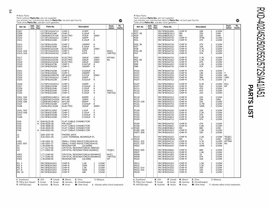
RXD-402/452/502/552/572S/A41/A51
54
PAR
TS LIST
C507 CC73FCH1H471J CHIP C 470PF JC508 CK73FB1E104K CHIP C 0.10UF KC509 CE04DW1C471M ELECTRO 470UF 16WVC510 CC73FCH1H101J CHIP C 100PF JC511 CK73FB1E104K CHIP C 0.10UF K
C512 CK73FB1H102K CHIP C 1000PF KC513 CK73FB1E104K CHIP C 0.10UF KC514 CE04KW1A101M ELECTRO 100UF 10WVC515, 516 CC73FCH1H470J CHIP C 47PF J M1E1C515, 516 CC73FCH1H470J CHIP C 47PF J YMXTEQ
C517 CE04KW1A101M ELECTRO 100UF 10WV KPYMXC517 CE04KW1A101M ELECTRO 100UF 10WV M1C518 CE04KW1A101M ELECTRO 100UF 10WVC519 CK73FB1E473K CHIP C 0.047UF KC520 CK73FB1H152K CHIP C 1500PF K
C521 CK73FB1H103K CHIP C 0.010UF KC522 CK73FB1H332K CHIP C 3300PF KC523 CE04HW1HR47M NP-ELEC 0.47UF 50WVC524 CC73FCH1H221J CHIP C 220PF JC525 CK73FB1H223K CHIP C 0.022UF K
C526 CC73FCH1H221J CHIP C 220PF JC527 CK73EB1H103K CHIP C 0.010UF KC528 CK73FB1E104K CHIP C 0.10UF KC530 CK73FB1E104K CHIP C 0.10UF K M1E1C530 CK73FB1E104K CHIP C 0.10UF K YMXTEQ
C531, 532 CQ93FMG1H821J MYLAR 820PF JC533, 534 CQ93FMG1H151K MYLAR 150PF KC535, 536 CQ93FMG1H821J MYLAR 820PF JC537 CK73FB1H103K CHIP C 0.010UF KC538 CE04LW1C101M ELECTRO 100UF 16WV
C541, 542 CK73FF1C105Z CHIP C 1.0UF ZC543~546 CK73FB1E104K CHIP C 0.10UF KC547 CK73EB1H103K CHIP C 0.010UF KC548 CK73FB1H103K CHIP C 0.010UF K
CN2 ✽ E40-8122-05 FLAT CABLE CONNECTORCN3 ✽ E40-8320-05 PIN ASSYCN4 E40-4908-05 FLAT CABLE CONNECTORCN5 E40-4920-05 FLAT CABLE CONNECTORCN5 ✽ E40-8332-05 FLAT CABLE CONNECTOR
J1 E63-1037-05 PHONO JACKJ2 E20-0321-05 LOCK TERMINAL BOARD(2P,F)
L501 L40-1001-31 SMALL FIXED INDUCTOR(10UH,K)L502, 503 L40-1001-17 SMALL FIXED INDUCTOR(10UH,K)X1 L78-0294-05 RESONATOR (10.000M)X2 L77-2173-05 CRYSTAL RESONATOR(32.768KHZ)X3 L77-2002-05 CRYSTAL RESONATOR(4.332MHZ) TEQE1
X501 L77-2190-05 CRYSTAL RESONATOR(16.9344MHZ) M1E1X501 L77-2190-05 CRYSTAL RESONATOR(16.9344MHZ) YMXTEQX501 L78-0299-05 RESONATOR (16.93M) KP
R1, 2 RK73FB2A102J CHIP R 1.0K J 1/10WR3, 4 RK73FB2A104J CHIP R 100K J 1/10WR5, 6 RK73FB2A102J CHIP R 1.0K J 1/10WR7, 8 RK73FB2A104J CHIP R 100K J 1/10WR9, 10 RK73FB2A183J CHIP R 18K J 1/10W
L : Scandinavia K : USA P : Canada R : Mexico C : China I : MalaysiaY : PX(Far East, Hawaii) T : Europe E : Europe G : Germany V : China(Shanghai)Y : AAFES(Europe) X : Australia Q : Russia H : Korea M : Other Areas indicates safety critical components.
L : Scandinavia K : USA P : Canada R : Mexico C : China I : MalaysiaY : PX(Far East, Hawaii) T : Europe E : Europe G : Germany V : China(Shanghai)Y : AAFES(Europe) X : Australia Q : Russia H : Korea M : Other Areas indicates safety critical components.
R22 RK73FB2A183J CHIP R 18K J 1/10WR27, 28 RD14NB2E151J RD 150 J 1/4WR29 RD14NB2E221J RD 220 J 1/4WR30 RK73FB2A474J CHIP R 470K J 1/10WR31 RK73FB2A473J CHIP R 47K J 1/10W
R35, 36 RK73FB2A473J CHIP R 47K J 1/10WR37 RK73FB2A223J CHIP R 22K J 1/10WR38 RK73FB2A472J CHIP R 4.7K J 1/10WR43~45 RK73FB2A472J CHIP R 4.7K J 1/10WR47 RK73FB2A473J CHIP R 47K J 1/10W
R52 RK73FB2A472J CHIP R 4.7K J 1/10WR61~64 RK73FB2A102J CHIP R 1.0K J 1/10WR79 RK73FB2A473J CHIP R 47K J 1/10WR80 RK73FB2A102J CHIP R 1.0K J 1/10WR88 RK73FB2A473J CHIP R 47K J 1/10W
R101 RK73FB2A473J CHIP R 47K J 1/10WR107 RK73FB2A133J CHIP R 13K J 1/10W TR107 RK73FB2A223J CHIP R 22K J 1/10W M1R107 RK73FB2A393J CHIP R 39K J 1/10W YMXR107 RK73FB2A472J CHIP R 4.7K J 1/10W Q
R107 RK73FB2A822J CHIP R 8.2K J 1/10W EE1R107 RK73FB2A913J CHIP R 91K J 1/10W KPR111 RK73FB2A473J CHIP R 47K J 1/10WR114 RK73FB2A471J CHIP R 470 J 1/10WR115 RK73FB2A221J CHIP R 220 J 1/10W
R119 RK73FB2A221J CHIP R 220 J 1/10WR121 RK73EB2B103J CHIP R 10K J 1/8WR122~129 RK73FB2A221J CHIP R 220 J 1/10WR131 RK73FB2A475J CHIP R 4.7M J 1/10WR132 RK73FB2A104J CHIP R 100K J 1/10W
R139 RK73FB2A103J CHIP R 10K J 1/10WR151 RK73FB2A222J CHIP R 2.2K J 1/10WR152 RK73FB2A473J CHIP R 47K J 1/10WR153 RK73FB2A562J CHIP R 5.6K J 1/10WR154 RK73FB2A471J CHIP R 470 J 1/10W
R155 RK73FB2A473J CHIP R 47K J 1/10WR156 RK73FB2A562J CHIP R 5.6K J 1/10WR165 RD14NB2E681J RD 680 J 1/4WR189, 190 RK73FB2A102J CHIP R 1.0K J 1/10WR207~209 RK73FB2A101J CHIP R 100 J 1/10W
R213 RK73FB2A222J CHIP R 2.2K J 1/10W TEQE1R216 RD14NB2E2R2J RD 2.2 J 1/4W TEQE1R221, 222 RK73FB2A472J CHIP R 4.7K J 1/10W KPYMXR221, 222 RK73FB2A472J CHIP R 4.7K J 1/10W M1R501 RK73FB2A224J CHIP R 220K J 1/10W
R502~505 RK73FB2A683J CHIP R 68K J 1/10WR507 RK73FB2A102J CHIP R 1.0K J 1/10WR508 RK73FB2A100J CHIP R 10 J 1/10WR509 RK73FB2A473J CHIP R 47K J 1/10WR510 RK73FB2A103J CHIP R 10K J 1/10W
R511 RK73FB2A152J CHIP R 1.5K J 1/10WR512 RK73FB2A222J CHIP R 2.2K J 1/10WR513, 514 RK73FB2A103J CHIP R 10K J 1/10WR515, 516 RK73FB2A101J CHIP R 100 J 1/10WR518 RK73FB2A153J CHIP R 15K J 1/10W
✽ New PartsParts without Parts No. are not supplied.Les articles non mentionnes dans le Parts No. ne sont pas fournis.Teile ohne Parts No. werden nicht geliefert.
$
Ref. No Add-ress
NewParts
Parts No. Description Desti-nation
Re-marks
✽ New PartsParts without Parts No. are not supplied.Les articles non mentionnes dans le Parts No. ne sont pas fournis.Teile ohne Parts No. werden nicht geliefert.
#
Ref. No Add-ress
NewParts Parts No. Description Desti-
nationRe-
marks
RXD-402(E) INT1P 99.6.9 7:25 PM y
[W 13

RXD-402/452/502/552/572S/A41/A5155
PAR
TS LIST
R520 RK73FB2A184J CHIP R 180K J 1/10WR522 RK73FB2A103J CHIP R 10K J 1/10WR523 RK73FB2A472J CHIP R 4.7K J 1/10WR525 RK73FB2A474J CHIP R 470K J 1/10WR526 RK73FB2A105J CHIP R 1.0M J 1/10W
R527 RK73FB2A153J CHIP R 15K J 1/10WR529 RK73FB2A473J CHIP R 47K J 1/10WR534 RK73FB2A471J CHIP R 470 J 1/10WR535 RK73FB2A105J CHIP R 1.0M J 1/10WR537 RK73FB2A561J CHIP R 560 J 1/10W M1E1
R537 RK73FB2A561J CHIP R 560 J 1/10W YMXTEQR538 RK73FB2A221J CHIP R 220 J 1/10W M1E1R538 RK73FB2A221J CHIP R 220 J 1/10W YMXTEQR539 RK73FB2A1R0J CHIP R 1 J 1/10WR540, 541 RK73FB2A332J CHIP R 3.3K J 1/10W
R542 RK73FB2A103J CHIP R 10K J 1/10WR543 RK73FB2A105J CHIP R 1.0M J 1/10WR544 RK73FB2A104J CHIP R 100K J 1/10WR545 RK73FB2A333J CHIP R 33K J 1/10WR546 RK73FB2A472J CHIP R 4.7K J 1/10W
R547 RK73FB2A153J CHIP R 15K J 1/10WR548 RK73FB2A104J CHIP R 100K J 1/10WR551 RK73FB2A472J CHIP R 4.7K J 1/10WR553 RD14NB2E2R2J RD 2.2 J 1/4WR555 RK73FB2A822J CHIP R 8.2K J 1/10W
R556 RK73FB2A103J CHIP R 10K J 1/10WR557 RK73FB2A432J CHIP R 4.3K J 1/10WR558 RK73FB2A512J CHIP R 5.1K J 1/10WR559 RK73FB2A103J CHIP R 10K J 1/10WR560 RK73FB2A224J CHIP R 220K J 1/10W
R561, 562 RK73FB2A912J CHIP R 9.1K J 1/10WR563~566 RK73FB2A103J CHIP R 10K J 1/10WR569, 570 RK73FB2A220J CHIP R 22 J 1/10WR571~574 RK73FB2A101J CHIP R 100 J 1/10WR575~578 RK73FB2A100J CHIP R 10 J 1/10W
R580 RK73FB2A472J CHIP R 4.7K J 1/10WR581 RK73FB2A101J CHIP R 100 J 1/10WVR1 R32-0038-05 SEMI FIXED VARIABLE RESISTORW5 R92-0670-05 CHIP R 0 OHM E2W5 R92-0670-05 CHIP R 0 OHM T1E1Q1
W7 R92-0670-05 CHIP R 0 OHMW67 R92-0679-05 CHIP R 0 OHMW195 R92-0670-05 CHIP R 0 OHM
D1~4 HSS104A DIODED1~4 1SS133 DIODED6, 7 HZS7.5N(B2) ZENER DIODED6, 7 MTZJ7.5(B) ZENER DIODED8 HZS3.9N(B2) ZENER DIODE
D8 MTZJ3.9(B) ZENER DIODED11, 12 RB721Q DIODED13, 14 HSS104A DIODED13, 14 1SS133 DIODED16 DAP202U DIODE
D16 MA142WA DIODE
L : Scandinavia K : USA P : Canada R : Mexico C : China I : MalaysiaY : PX(Far East, Hawaii) T : Europe E : Europe G : Germany V : China(Shanghai)Y : AAFES(Europe) X : Australia Q : Russia H : Korea M : Other Areas indicates safety critical components.
L : Scandinavia K : USA P : Canada R : Mexico C : China I : MalaysiaY : PX(Far East, Hawaii) T : Europe E : Europe G : Germany V : China(Shanghai)Y : AAFES(Europe) X : Australia Q : Russia H : Korea M : Other Areas indicates safety critical components.
D16 1SS300 DIODED501, 502 MA111 DIODED501, 502 1SS355 DIODED504 DAN202U DIODED504 MA142WK DIODE
D504 1SS301 DIODEIC1 ✽ M30622MA-173FP MI-COM ICIC2 M62492FP MOS-ICIC3 SAA6579T/R ANALOGUE IC TEQE1IC4 ✽ S-80840ANY ANALOGUE IC
IC5 CXA1571M ANALOGUE ICIC6 BA5979S ANALOGUE ICIC7 CXD2587Q MOS-ICIC8, 9 TA8409S MOS-ICQ1 KTC3199(Y,GR) TRANSISTOR
Q1 2SC2785(F,E) TRANSISTORQ2 2SB1412F5(Q,R) TRANSISTOR KPYMXQ2 2SB1412F5(Q,R) TRANSISTOR M1Q3 DTC124EUA DIGITAL TRANSISTOR KPYMXQ3 DTC124EUA DIGITAL TRANSISTOR M1
Q3 ✽ KRC103S TRANSISTOR KPYMXQ3 ✽ KRC103S TRANSISTOR M1Q3 UN5212 DIGITAL TRANSISTOR KPYMXQ3 UN5212 DIGITAL TRANSISTOR M1Q4, 5 DTA113ZUA DIGITAL TRANSISTOR
Q4, 5 UN5119 DIGITAL TRANSISTORQ7 DTA143TUA DIGITAL TRANSISTOR TEQE1Q7 UN5116 DIGITAL TRANSISTOR TEQE1Q8 DTC124EUA DIGITAL TRANSISTORQ8 ✽ KRC103S TRANSISTOR
Q8 UN5212 DIGITAL TRANSISTORQ10 DTA113ZUA DIGITAL TRANSISTORQ10 UN5119 DIGITAL TRANSISTORQ11, 12 ✽ 2SD2144S(U,V) TRANSISTOR TEQE1Q501 2SA954(L,K) TRANSISTOR
Q502 DTC113ZUA DIGITAL TRANSISTORQ502 UN5219 DIGITAL TRANSISTORQ503 ✽ KTA1273 TRANSISTORQ503 2SA1534A(R,S) TRANSISTORQ504 DTC113ZUA DIGITAL TRANSISTOR
Q504 UN5219 DIGITAL TRANSISTORQ505 2SB1640 TRANSISTOR
A1 ✽ W02-2673-05 TUNER ASSY KPYMXA1 ✽ W02-2674-05 TUNER ASSY EE1A1 ✽ W02-2675-05 TUNER ASSY QA1 ✽ W02-2676-05 TUNER ASSY M1A1 ✽ W02-2685-05 TUNER ASSY T
A501 W02-1114-05 OSCILLATING MODULE M1E1A501 W02-1114-05 OSCILLATING MODULE YMXTEQ
D51, 52 B30-2546-05 LED(RED3(80))D53 ✽ B30-2548-05 LED(GRN5(80),HI B) 57D54~58 ✽ B30-2547-05 LED(RED5(80),HI B)D59~64 B30-2546-05 LED(RED3(80)) TEQE1
✽ New PartsParts without Parts No. are not supplied.Les articles non mentionnes dans le Parts No. ne sont pas fournis.Teile ohne Parts No. werden nicht geliefert.
^
Ref. No Add-ress
NewParts
Parts No. Description Desti-nation
Re-marks
✽ New PartsParts without Parts No. are not supplied.Les articles non mentionnes dans le Parts No. ne sont pas fournis.Teile ohne Parts No. werden nicht geliefert.
%
Ref. No Add-ress
NewParts Parts No. Description Desti-
nationRe-
marks
DISPLAY UNIT (X14-493X-XX)
RXD-402(E) INT1P 99.6.9 7:25 PM y
[W 12
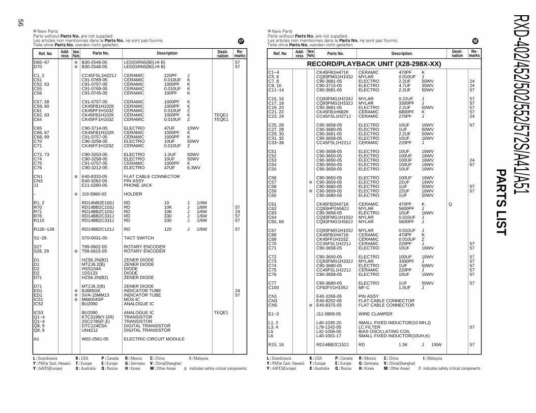
RXD-402/452/502/552/572S/A41/A51
56
PAR
TS LIST
D65~67 ✽ B30-2548-05 LED(GRN5(80),HI B) 57D70 ✽ B30-2548-05 LED(GRN5(80),HI B) 57
C1, 2 CC45FSL1H221J CERAMIC 220PF JC51 C91-0769-05 CERAMIC 0.010UF KC52, 53 C91-0757-05 CERAMIC 1000PF KC55 C91-0769-05 CERAMIC 0.010UF KC56 C91-0745-05 CERAMIC 100PF K
C57, 58 C91-0757-05 CERAMIC 1000PF KC59, 60 CK45FB1H102K CERAMIC 1000PF KC61 CK45FF1H103Z CERAMIC 0.010UF ZC62, 63 CK45FB1H102K CERAMIC 1000PF K TEQE1C64 CK45FF1H103Z CERAMIC 0.010UF Z TEQE1
C65 C90-3714-05 ELECTRO 47UF 10WVC66, 67 CK45FB1H102K CERAMIC 1000PF KC68, 69 C91-0757-05 CERAMIC 1000PF KC70 C90-3258-05 ELECTRO 10UF 50WVC71 CK45FF1H103Z CERAMIC 0.010UF Z
C72, 73 C90-3253-05 ELECTRO 1.0UF 50WVC74 C90-3258-05 ELECTRO 10UF 50WVC75 C91-0757-05 CERAMIC 1000PF KC76 C90-3212-05 ELECTRO 47UF 6.3WV
CN1 ✽ E40-8333-05 FLAT CABLE CONNECTORCN3 E40-3262-05 PIN ASSYJ1 E11-0280-05 PHONE JACK
- ✽ J19-5960-03 HOLDER
R1, 2 RD14NB2E100J RD 10 J 1/4WR70 RD14BB2C103J RD 10K J 1/6W 57R71 RD14BB2C103J RD 10K J 1/6W 24R76 RD14BB2C331J RD 330 J 1/6W 57R110 RD14BB2C331J RD 330 J 1/6W 57
R126~128 RD14BB2C121J RD 120 J 1/6W 57
S1~26 S70-0031-05 TACT SWITCH
S27 T99-0602-05 ROTARY ENCODERS28, 29 ✽ T99-0615-05 ROTARY ENCODER
D1 HZS6.2N(B2) ZENER DIODED1 MTZJ6.2(B) ZENER DIODED2 HSS104A DIODED2 1SS133 DIODED71 HZS6.2N(B2) ZENER DIODE
D71 MTZJ6.2(B) ZENER DIODEED1 ✽ BJ665GK INDICATOR TUBE 24ED1 ✽ SVA-15MM13 INDICATOR TUBE 57IC51 ✽ M66004SP MOS-ICIC52 BU2090 ANALOGUE IC
IC53 BU2090 ANALOGUE IC TEQE1Q1~4 KTC3199(Y,GR) TRANSISTORQ1~4 2SC2785(F,E) TRANSISTORQ8, 9 DTC124ESA DIGITAL TRANSISTORQ8, 9 UN4212 DIGITAL TRANSISTOR
A1 W02-2561-05 ELECTRIC CIRCUIT MODULE
L : Scandinavia K : USA P : Canada R : Mexico C : China I : MalaysiaY : PX(Far East, Hawaii) T : Europe E : Europe G : Germany V : China(Shanghai)Y : AAFES(Europe) X : Australia Q : Russia H : Korea M : Other Areas indicates safety critical components.
L : Scandinavia K : USA P : Canada R : Mexico C : China I : MalaysiaY : PX(Far East, Hawaii) T : Europe E : Europe G : Germany V : China(Shanghai)Y : AAFES(Europe) X : Australia Q : Russia H : Korea M : Other Areas indicates safety critical components.
C1~4 CK45FB1H471K CERAMIC 470PF KC5, 6 CQ93FMG1H103J MYLAR 0.010UF JC7, 8 C90-3681-05 ELECTRO 2.2UF 50WV 24C9, 10 C90-3715-05 ELECTRO 4.7UF 35WV 24C11~14 C90-3681-05 ELECTRO 2.2UF 50WV 57
C15, 16 CQ93FMG1H224J MYLAR 0.22UF J 57C17, 18 CQ93FMG1H332J MYLAR 3300PF J 57C19, 20 C90-3681-05 ELECTRO 2.2UF 50WV 57C21, 22 CK45FB1H682K CERAMIC 6800PF K 57C23, 24 CC45FSL1H271J CERAMIC 270PF J 24
C25, 26 C90-3658-05 ELECTRO 10UF 16WV 57C27, 28 C90-3680-05 ELECTRO 1UF 50WVC29, 30 C90-3681-05 ELECTRO 2.2UF 50WVC31, 32 C90-3658-05 ELECTRO 10UF 16WVC33~36 CC45FSL1H221J CERAMIC 220PF J
C51 C90-3658-05 ELECTRO 10UF 16WVC52 C90-3650-05 ELECTRO 100UF 16WVC53 C90-3650-05 ELECTRO 100UF 16WV 24C54 C90-3650-05 ELECTRO 100UF 16WV 57C55 C90-3658-05 ELECTRO 10UF 16WV
C56 C90-3650-05 ELECTRO 100UF 16WVC57 ✽ C90-3659-05 ELECTRO 22UF 16WVC58 C90-3680-05 ELECTRO 1UF 50WV 57C59 ✽ C90-3659-05 ELECTRO 22UF 16WV 57C60 C90-3680-05 ELECTRO 1UF 50WV
C61 CK45FB2H471K CERAMIC 470PF K QC62 CQ93HP2A562J MYLAR 5600PF JC63 C90-3658-05 ELECTRO 10UF 16WVC64 CQ93FMG1H103J MYLAR 0.010UF JC65, 66 CQ93FMG1H562J MYLAR 5600PF J
C67 CQ93FMG1H103J MYLAR 0.010UF JC68 CK45FB1H471K CERAMIC 470PF KC69 CK45FF1H103Z CERAMIC 0.010UF ZC70 CC45FSL1H221J CERAMIC 220PF J 57C71 C90-3658-05 ELECTRO 10UF 16WV 57
C72 C90-3650-05 ELECTRO 100UF 16WV 57C73 CQ93FMG1H332J MYLAR 3300PF J 57C74 C90-3680-05 ELECTRO 1UF 50WV 57C75 CC45FSL1H221J CERAMIC 220PF J 57C76 C90-3658-05 ELECTRO 10UF 16WV 57
C77 C90-3680-05 ELECTRO 1UF 50WV 57C100 CF92FV1H105J MF-C 1.0UF J
CN1 E40-3269-05 PIN ASSYCN3 E40-8252-05 FLAT CABLE CONNECTORCN5 ✽ E40-8375-05 FLAT CABLE CONNECTOR
E1~3 J11-0809-05 WIRE CLAMPER
L1, 2 L40-1035-20 SMALL FIXED INDUCTOR(10 MH,J)L3, 4 L79-1242-05 LC FILTER 57L5 L32-1006-05 BIAS OSCILLATING COILL6 L40-1001-17 SMALL FIXED INDUCTOR(10UH,K)
R15, 16 RD14BB2C152J RD 1.5K J 1/6W 57
✽ New PartsParts without Parts No. are not supplied.Les articles non mentionnes dans le Parts No. ne sont pas fournis.Teile ohne Parts No. werden nicht geliefert.
*
Ref. No Add-ress
NewParts
Parts No. Description Desti-nation
Re-marks
✽ New PartsParts without Parts No. are not supplied.Les articles non mentionnes dans le Parts No. ne sont pas fournis.Teile ohne Parts No. werden nicht geliefert.
&
Ref. No Add-ress
NewParts Parts No. Description Desti-
nationRe-
marks
RECORD/PLAYBACK UNIT (X28-298X-XX)
RXD-402(E) INT1P 99.6.9 7:25 PM y
[W 9

RXD-402/452/502/552/572S/A41/A5157
PAR
TS LIST
R17, 18 RD14BB2C103J RD 10K J 1/6W 24R19, 20 RD14BB2C391J RD 390 J 1/6W 24R21, 22 RD14BB2C103J RD 10K J 1/6W 24R23, 24 RD14BB2C152J RD 1.5K J 1/6W 57R27, 28 RD14BB2C392J RD 3.9K J 1/6W 57
R33, 34 RD14BB2C912J RD 9.1K J 1/6W 57R39, 40 RD14BB2C563J RD 56K J 1/6W 57R51, 52 RD14NB2E100J RD 10 J 1/4WR53 RD14NB2E100J RD 10 J 1/4W 57R54 RD14NB2E100J RD 10 J 1/4W 24
R55 RD14NB2E100J RD 10 J 1/4WR56 RD14NB2E102J RD 1.0K J 1/4WR60 RD14BB2C183J RD 18K J 1/6W 57R61, 62 RD14BB2C223J RD 22K J 1/6W 57R71 RD14NB2E152J RD 1.5K J 1/4W
R97, 98 RD14BB2C103J RD 10K J 1/6W 57R99 RD14BB2C224J RD 220K J 1/6W 57R100 RD14BB2C332J RD 3.3K J 1/6W 57R101 RD14BB2C104J RD 100K J 1/6W 57R102 RD14BB2C103J RD 10K J 1/6W 57
R103 RD14BB2C472J RD 4.7K J 1/6W 57R104 RD14BB2C332J RD 3.3K J 1/6W 57R105 RD14BB2C102J RD 1.0K J 1/6W 57R106 RD14NB2E471J RD 470 J 1/4W 57R113, 114 RD14BB2C302J RD 3.0K J 1/6W 24
R125 RD14BB2C103J RD 10K J 1/6W 57R130 RD14BB2C104J RD 100K J 1/6W 57VR1, 2 ✽ R32-0031-05 SEMI FIXED VARIABLE RESISTORVR3, 4 R32-0042-05 SEMI FIXED VARIABLE RESISTORVR5 R32-0036-05 SEMI FIXED VARIABLE RESISTOR
VR7, 8 ✽ R32-0031-05 SEMI FIXED VARIABLE RESISTOR
D1~4 HSS104A DIODED1~4 1SS133 DIODED5 HZS5.6N(B2) ZENER DIODED5 MTZJ5.6(B) ZENER DIODED6, 7 HSS104A DIODE 57
D6, 7 1SS133 DIODE 57D8 HZS5.1N(B2) ZENER DIODED8 MTZJ5.1(B) ZENER DIODED9, 10 HSS104A DIODE 57D9, 10 1SS133 DIODE 57
IC1 HA12219NT ANALOGUE ICIC2 HA12136A ANALOGUE IC 57IC3 BA3126N ANALOGUE ICIC4 ✽ HD74HC166P MOS-ICIC4 TC74HC166AP MOS-IC
IC5 NJM4565L ANALOGUE IC 24IC6 NJM4565L ANALOGUE IC 57Q1 ✽ KTC3205 TRANSISTORQ1 2SC3940A(R,S) TRANSISTORQ2~5 DTC124ESA DIGITAL TRANSISTOR
Q2~5 ✽ KRC103M TRANSISTORQ6 2SA1286-T11 TRANSISTORQ7 DTC124ESA DIGITAL TRANSISTOR
L : Scandinavia K : USA P : Canada R : Mexico C : China I : MalaysiaY : PX(Far East, Hawaii) T : Europe E : Europe G : Germany V : China(Shanghai)Y : AAFES(Europe) X : Australia Q : Russia H : Korea M : Other Areas indicates safety critical components.
L : Scandinavia K : USA P : Canada R : Mexico C : China I : MalaysiaY : PX(Far East, Hawaii) T : Europe E : Europe G : Germany V : China(Shanghai)Y : AAFES(Europe) X : Australia Q : Russia H : Korea M : Other Areas indicates safety critical components.
Q7 ✽ KRC103M TRANSISTORQ8 2SA1286-T11 TRANSISTORQ9 DTC124ESA DIGITAL TRANSISTORQ9 KRC103M TRANSISTORQ10 2SA1286-T11 TRANSISTOR
Q11, 12 KTC3199(Y,GR) TRANSISTORQ11, 12 2SC2785(F,E) TRANSISTORQ13, 14 2SC1845(F,E) TRANSISTOR QQ15 DTA124ESA DIGITAL TRANSISTOR QQ15 ✽ KRA103M TRANSISTOR Q
Q16 DTC124ESA DIGITAL TRANSISTOR QQ16 ✽ KRC103M TRANSISTOR QQ21 DTA124ESA DIGITAL TRANSISTORQ21 ✽ KRA103M TRANSISTORQ22 DTC124ESA DIGITAL TRANSISTOR
Q22 KRC103M TRANSISTORQ23~26 KTC3199(Y,GR) TRANSISTORQ23~26 2SC2785(F,E) TRANSISTORQ27, 28 DTC124ESA DIGITAL TRANSISTORQ27, 28 ✽ KRC103M TRANSISTOR
Q29 DTA124ESA DIGITAL TRANSISTORQ29 ✽ KRA103M TRANSISTOR
103 1B D13-1763-04 GEAR (MIDDLE)104 1B D13-1765-03 GEAR (DRIVING)106 2A D10-3659-04 ROD (GUIDE)
113 3A E40-3264-05 PIN ASSY
111 2A J90-0844-03 GUIDE (RAIL)
110 3A S74-0065-05 LEAF SWITCH
DM 2B A11-1114-08 SUB CHASSIS ASSYFM 3B T42-0872-08 FEED MOTOR ASSYPU 1A T25-0050-05 PICKUP KCP1H
1 3D ✽ A10-3478-08 CHASSIS6 3D ✽ D10-3891-08 FRICTION ARM7 3D ✽ D13-1940-08 GEAR8 3D ✽ J31-0882-08 COLLAR(LOAD)9 2C ✽ D13-1941-08 GEAR
11 2C ✽ D15-0418-08 PULLEY GEAR12 2C ✽ D16-0731-08 DRIVE BELT13 1C ✽ J99-0814-08 TRAY (SLIDE)14 2C D13-1599-08 GEAR (IDLER)15 2D ✽ G09-0670-08 WIRE SPRING
20 2C ✽ B30-2553-08 LED (SIR-34ST3F)21 2D D13-1604-08 GEAR (HELICAL)22 1C ✽ D10-3892-08 LOCK ARM23 1D G01-3931-08 EXTENSION SPRING (BRAKE)24 1D ✽ J90-0870-08 SENSOR GUIDE
25 1D ✽ T95-0162-08 PHOTO TRANSISTOR (RPT-38PB3F)27 1C S33-1022-05 PUSH SWITCH (SPPB12)29 1C ✽ J99-0815-08 TRAY (ROTARY)31 1D ✽ J21-6729-08 CLAMPER BKT
✽ New PartsParts without Parts No. are not supplied.Les articles non mentionnes dans le Parts No. ne sont pas fournis.Teile ohne Parts No. werden nicht geliefert.
)
Ref. No Add-ress
NewParts
Parts No. Description Desti-nation
Re-marks
✽ New PartsParts without Parts No. are not supplied.Les articles non mentionnes dans le Parts No. ne sont pas fournis.Teile ohne Parts No. werden nicht geliefert.
(
Ref. No Add-ress
NewParts Parts No. Description Desti-
nationRe-
marks
CD MECHANISM UNIT (D40-1500-05) : KCTB1H
CD MECHANISM UNIT (D40-1619-05) : MGC-E9001
RXD-402(E) INT1P 99.6.9 7:25 PM y
[W 8
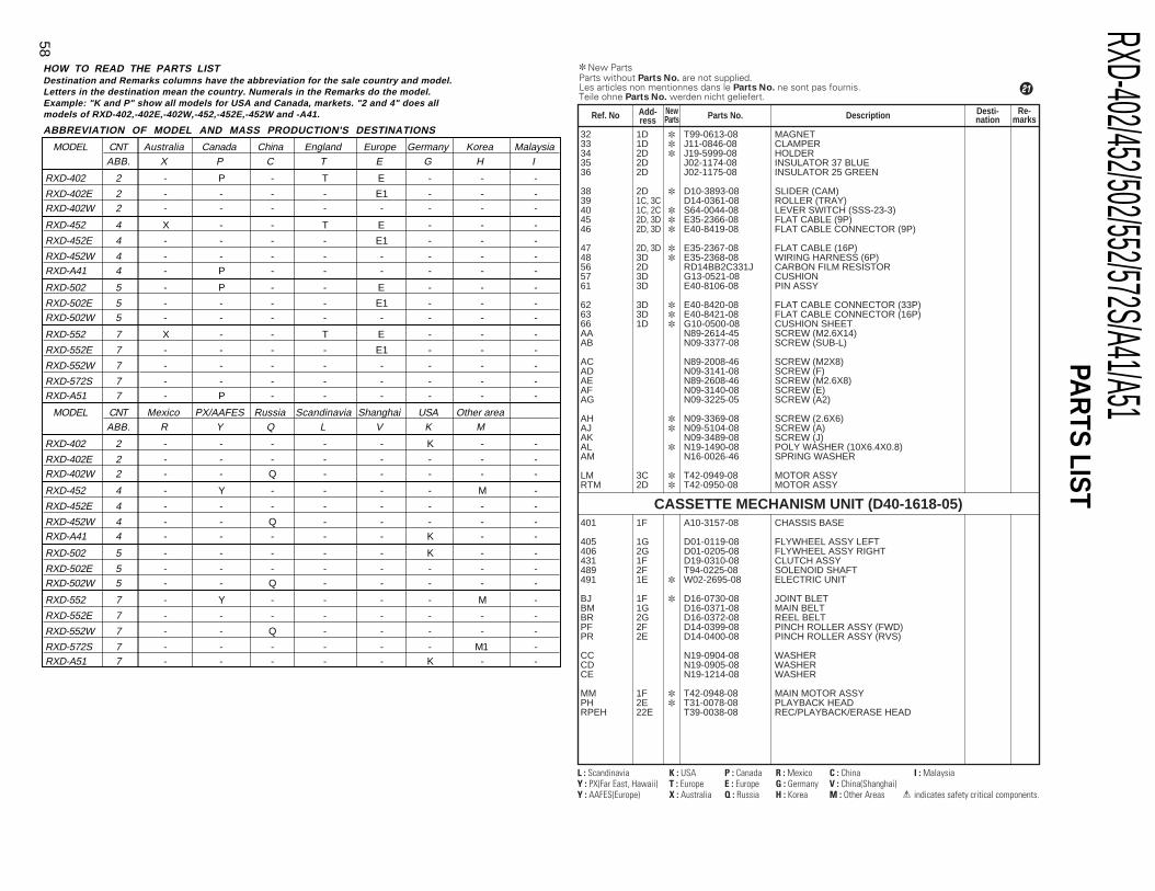
RXD-402/452/502/552/572S/A41/A51
58
PAR
TS LIST
L : Scandinavia K : USA P : Canada R : Mexico C : China I : MalaysiaY : PX(Far East, Hawaii) T : Europe E : Europe G : Germany V : China(Shanghai)Y : AAFES(Europe) X : Australia Q : Russia H : Korea M : Other Areas indicates safety critical components.
32 1D ✽ T99-0613-08 MAGNET33 1D ✽ J11-0846-08 CLAMPER34 2D ✽ J19-5999-08 HOLDER35 2D J02-1174-08 INSULATOR 37 BLUE36 2D J02-1175-08 INSULATOR 25 GREEN
38 2D ✽ D10-3893-08 SLIDER (CAM)39 1C, 3C D14-0361-08 ROLLER (TRAY)40 1C, 2C ✽ S64-0044-08 LEVER SWITCH (SSS-23-3)45 2D, 3D ✽ E35-2366-08 FLAT CABLE (9P)46 2D, 3D ✽ E40-8419-08 FLAT CABLE CONNECTOR (9P)
47 2D, 3D ✽ E35-2367-08 FLAT CABLE (16P)48 3D ✽ E35-2368-08 WIRING HARNESS (6P)56 2D RD14BB2C331J CARBON FILM RESISTOR57 3D G13-0521-08 CUSHION61 3D E40-8106-08 PIN ASSY
62 3D ✽ E40-8420-08 FLAT CABLE CONNECTOR (33P)63 3D ✽ E40-8421-08 FLAT CABLE CONNECTOR (16P)66 1D ✽ G10-0500-08 CUSHION SHEETAA N89-2614-45 SCREW (M2.6X14)AB N09-3377-08 SCREW (SUB-L)
AC N89-2008-46 SCREW (M2X8)AD N09-3141-08 SCREW (F)AE N89-2608-46 SCREW (M2.6X8)AF N09-3140-08 SCREW (E)AG N09-3225-05 SCREW (A2)
AH ✽ N09-3369-08 SCREW (2.6X6)AJ ✽ N09-5104-08 SCREW (A)AK N09-3489-08 SCREW (J)AL ✽ N19-1490-08 POLY WASHER (10X6.4X0.8)AM N16-0026-46 SPRING WASHER
LM 3C ✽ T42-0949-08 MOTOR ASSYRTM 2D ✽ T42-0950-08 MOTOR ASSY
401 1F A10-3157-08 CHASSIS BASE
405 1G D01-0119-08 FLYWHEEL ASSY LEFT406 2G D01-0205-08 FLYWHEEL ASSY RIGHT431 1F D19-0310-08 CLUTCH ASSY489 2F T94-0225-08 SOLENOID SHAFT491 1E ✽ W02-2695-08 ELECTRIC UNIT
BJ 1F ✽ D16-0730-08 JOINT BLETBM 1G D16-0371-08 MAIN BELTBR 2G D16-0372-08 REEL BELTPF 2F D14-0399-08 PINCH ROLLER ASSY (FWD)PR 2E D14-0400-08 PINCH ROLLER ASSY (RVS)
CC N19-0904-08 WASHERCD N19-0905-08 WASHERCE N19-1214-08 WASHER
MM 1F ✽ T42-0948-08 MAIN MOTOR ASSYPH 2E ✽ T31-0078-08 PLAYBACK HEADRPEH 22E T39-0038-08 REC/PLAYBACK/ERASE HEAD
✽ New PartsParts without Parts No. are not supplied.Les articles non mentionnes dans le Parts No. ne sont pas fournis.Teile ohne Parts No. werden nicht geliefert.
¡
Ref. No Add-ress
NewParts Parts No. Description Desti-
nationRe-
marks
CASSETTE MECHANISM UNIT (D40-1618-05)
HOW Destination and Remarks columns have the abbreviation for the sale country and model.Letters in the destination mean the country. Numerals in the Remarks do the model.Example: "K and P" show all models for USA and Canada, markets. "2 and 4" does allmodels of RXD-402,-402E,-402W,-452,-452E,-452W and -A41.
TO READ THE PARTS LIST
ABBREVIATION OF MODEL AND MASS PRODUCTION'S DESTINATIONS
MODEL CNT Australia Canada China England Europe Germany Korea MalaysiaABB. X P C T E G H I
RXD-402 2 - P - T E - - -
RXD-402E 2 - - - - E1 - - -RXD-402W 2 - - - - - - - -
RXD-452 4 X - - T E - - -
RXD-452E 4 - - - - E1 - - -
RXD-452W 4 - - - - - - - -RXD-A41 4 - P - - - - - -
RXD-502 5 - P - - E - - -
RXD-502E 5 - - - - E1 - - -RXD-502W 5 - - - - - - - -
RXD-552 7 X - - T E - - -
RXD-552E 7 - - - - E1 - - -
RXD-552W 7 - - - - - - - -
RXD-572S 7 - - - - - - - -RXD-A51 7 - P - - - - - -
MODEL CNT Mexico PX/AAFES Russia Scandinavia Shanghai USA Other areaABB. R Y Q L V K M
RXD-402 2 - - - - - K - -
RXD-402E 2 - - - - - - - -RXD-402W 2 - - Q - - - - -
RXD-452 4 - Y - - - - M -
RXD-452E 4 - - - - - - - -
RXD-452W 4 - - Q - - - - -RXD-A41 4 - - - - - K - -
RXD-502 5 - - - - - K - -
RXD-502E 5 - - - - - - - -RXD-502W 5 - - Q - - - - -
RXD-552 7 - Y - - - - M -
RXD-552E 7 - - - - - - - -
RXD-552W 7 - - Q - - - - -
RXD-572S 7 - - - - - - M1 -RXD-A51 7 - - - - - K - -
RXD-402(E) INT1P 99.6.9 7:25 PM y
[W 5

RXD-402/452/502/552/572S/A41/A51
59
SPECIFICATIONS
[ Amplifier section ]
(XD-5...Series)Rated power output (For U.S.A. and Canada)
80 watts per channel minimum RMS, both channels driven,at 6 W form 40 Hz to 15 kHz with no more than 0.9 % totalharmonic distortion. (FTC)
Effective output power during STEREO operation(Except for U.S.A. and Canada)
1 kHz, 10 % T.H.D., 6 W ............................... 100 W + 100 WRated output power during STEREO operation
(For U.K., Europe and Russia)(DIN) 1 kHz, 0.7 % T.H.D., 6 W ............................ 70 W + 70 W
(Other countories)1 kHz, 1.0 % T.H.D., 6 W ...................................... 80 W + 80 W
(XD-4...Series)Rated power output (For U.S.A. and Canada)
50 watts per channel minimum RMS, both channels driven,at 6 W form 40 Hz to 15 kHz with no more than 0.9 % totalharmonic distortion. (FTC)
Effective output power during STEREO operation(Except for U.S.A. and Canada)
1 kHz, 10 % T.H.D., 6 W ................................... 70 W + 70 WRated output power during STEREO operation
(For U.K., Europe and Russia)(DIN) 1 kHz, 0.7 % T.H.D., 6 W ............................ 50 W + 50 W
(Other countories)1 kHz, 1.0 % T.H.D., 6 W ...................................... 55 W + 55 W
Signal to noise ratioMD/DVD INPUT ........................................... 90 dB (IHF’ 66)
Input sensitivity / inpedanceMD/DVD INPUT ................. (XD-5...Series) 270 mV / 47 kW
(XD-4...Series) 300 mV / 47 kWOutput level / impedance
SUPER WOOFER PREOUT .... (XD-5...Series) 1.3 V / 620 W(XD-4...Series) 1.0 V / 620 W
[ Tuner section ]FM tuner sectionTuning frequency range ........................... 87.5 MHz ~ 108 MHz
(For Russia) ........................................... 65.0 MHz ~ 74.0 MHz
MW (AM) Tuner sectionTuning frequency range
For U.K., Europe and Russia ................... 531 kHz ~ 1,602 kHzOther countories
9 kHz step ............................................ 531 kHz ~ 1,602 kHz10 kHz step ..........................................530 kHz ~ 1,610 kHz
For U.S.A. and Canada ........................... 530 kHz ~ 1,700 kHz
LW Tuner section (For U.K. and Russia)Tuning frequency range ............................... 153 kHz ~ 279 kHz
SW Tuner section (XD-572S only)Tuning frequency range ............................ 5.9 MHz ~ 17.9 MHz
NotesNotes
1.KENWOOD follows a policy of continuous advancements in development. For this reason specifications may bechanged without notice.
2.Sufficient performance may not be possible at very low temperatures (0¡C or less).
[ Cassette deck section ]Track ................................................... 4-track, 2-channel stereoRecording system .............................................. AC bias system
(Frequency: 105 kHz)Heads
A deckPlayback head ............................................................ 1B deckPlayback / recording head .......................................... 1
Erasing head ...................................................................... 1Fast winding time ...................................... Approx. 115 seconds
(C-60 tape)
[ CD player section ]Laser ......................................................... Semiconductor laserWow & Flutter ............................. Less than unmeasurable Limit(Except for U.S.A. and Canada)Digital output (Optical) ............................... - 15 dBm ~ - 21 dBm
(Wave length 660 nm)
[ General ]Power consumption ................................. (XD-5...Series) 200 W
(XD-4...Series) 150 WDimensions ........................................ W : 280 mm (11”)
H : 330 mm (13”)D : 390 mm (15-3/8”)
Weight (net) ................................ (XD-5...Series) 9.9 kg (21.8 lb)(XD-4...Series) 9.2 kg (20.2 lb)
Main unit
RXD-402(E) INT1P 99.6.9 7:25 PM y [ W 4

14-6,Dogenzaka 1-chome, Shibuya-ku, Tokyo, 150-8501 Japan
KENWOOD SERVICE CORPORATIONP.O BOX 22745, 2201 East Dominguez St., Long Beach, CA 90801-5745, U.S.A.
KENWOOD ELECTRONICS CANADA INC.6070 Kestrel Road, Mississauga, Ontario, Canada L5T 1S8
KENWOOD ELECTRONICS LATIN AMERICA S.A.P.O BOX 55-2791, Piso 6 plaza Chase, Cl. 47 y Aquilino de la Guardia Panama, Republic de Panama
KENWOOD ELECTRONICS BRASIL LTDA.Av. Moema, 170-17˚, Andar-Cobertura “B”, Ed. Maximum Service Center, 04077-020Moema, São Paulo-SP-Brasil
KENWOOD ELECTRONICS U.K. LIMITEDKENWOOD House, Dwight Road, Watford, Herts., WD1 8EB., United Kingdom
KENWOOD ELECTRONICS BELGUM N.V.Meachelsesteenweg 418, B-1930 Zaventem, Belgium
KENWOOD ELECTRONICS DEUTSCHLAND GMBHRembrücker Str. 15, 63150 Heusenstamm, Germany
KENWOOD ELECTRONICS FRANCE S.A.13 Boulevard Ney, 75018 Paris, France
KENWOOD ELECTRONICS ITALIA S.p.A.Via G. Sirtori, 7/9 20129, Milano, ltaly
KENWOOD IBÉRICA S.A.Bolivia, 239-08020 Barcelona, Spain
KENWOOD ELECTRONICS AUSTRALIA PTY. LTD.(A.C.N. 001499 074) P.O Box 504, 8 Figtree Drive, Australia Centre, Homebush, N.S.W. 2140, Australia
KENWOOD & LEE ELECTRONICS, LTD.Unit 3712-3724, Level 37, Tower 1, Metroplaza, 223 Hing Fong Road, Kwai Fong N.T., Hong Kong
KENWOOD ELECTRONICS GULF FZEP.O.Box 61318, Jebel Ali, Dubai, U.A.E.
KENWOOD ELECTRONICS SINGAPORE PTE LTD. No. 1 Genting Lane #02-02, KENWOOD Building, Singapore, 349544
KENWOOD ELECTRONICS (MALAYSIA) SDN BHD.#4.01 Level 4, Wisma Academy Lot 4A, Jalan 19/1 46300 Petaling Jaya Selangor Darul EhsanMalaysia
KENWOOD ELECTRONICS (THAILAND) CO., LTD.2019 New Pechburi Road, Bangkapi, Huaykwang, Bangkok, 10320 Thailand
RXD-402/452/502/552/572S/A41/A51SPECIFICATIONS
Note:Component and circuit are subject to modification to insure best operation under differing local conditions. This manual is based on General mar-ket(M) standard, and provides information on regional circuit modification through use of alternate schematic diagrams, and information onregional component variations through use of parts list.
[ Amplifier section ]
(XD-A51)Rated power output (For U.S.A. and Canada)
80 watts per channel minimum RMS, both channels driven,at 6 W form 40 Hz to 15 kHz with no more than 0.9 % totalharmonic distortion. (FTC)
(XD-A41)Rated power output (For U.S.A. and Canada)
50 watts per channel minimum RMS, both channels driven,at 6 W form 40 Hz to 15 kHz with no more than 0.9 % totalharmonic distortion. (FTC)
Signal to noise ratioMD/DVD INPUT ........................................... 90 dB (IHF’ 66)
Input sensitivity / inpedanceMD/DVD INPUT .......................... (XD-A51) 270 mV / 47 kW
(XD-A41) 300 mV / 47 kWOutput level / impedance
SUPER WOOFER PREOUT ........... (XD-A51) 1.3 V / 620 W (XD-A41) 1.0 V / 620 W
[ Tuner section ]FM tuner sectionTuning frequency range ........................ 87.5 MHz ~ 108.0 MHz
AM Tuner sectionTuning frequency range ............................. 530 kHz ~ 1,700 kHz
[ Cassette deck section ]Track ................................................... 4-track, 2-channel stereoRecording system .............................................. AC bias system
(Frequency: 105 kHz)Heads
A deckPlayback head ............................................................ 1B deckPlayback / recording head .......................................... 1
Erasing head ...................................................................... 1Fast winding time ...................................... Approx. 115 seconds
(C-60 tape)
NotesNotes
1.KENWOOD follows a policy of continuous advancements in development. For this reason specifications may bechanged without notice.
2.Sufficient performance may not be possible at very low temperatures (0¡C or less).
[ CD player section ]Laser ......................................................... Semiconductor laserWow & Flutter ............................. Less than unmeasurable Limit
[ General ]Power consumption .......................................... (XD-A51) 200 W
(XD-A41) 150 WDimensions ........................................ W : 280 mm (11”)
H : 330 mm (13”)D : 390 mm (15-3/8”)
Weight (net) ......................................... (XD-A51) 9.9 kg (21.8 lb)(XD-A41) 9.2 kg (20.2 lb)
Main unit
RXD-402(E) INT1P 99.6.9 7:25 PM y [ W 1
Related Documents