© 2000-12 PRINTED IN JAPAN B51-8558-00 (N) 889 ALL MODE MULTI-BAND TRANSCEIVER TS-2000/X SERVICE MANUAL CIRCUIT DESCRIPTION ............................. 2 DESCRIPTION OF COMPONENTS ......... 24 SEMICONDUCTOR DATA ....................... 34 PARTS LIST .............................................. 51 EXPLODED VIEW ..................................... 93 PACKING .................................................. 97 ADJUSTMENT ......................................... 98 TERMINAL FUNCTION .......................... 124 WIRING .................................................. 133 PC BOARD VIEWS / CIRCUIT DIAGRAMS FILTER UNIT (X51-315X-XX) ............. 135 FINAL UNIT (X45-360X-XX) .............. 137 DISPLAY UNIT (X54-3320-00) ........... 151 CONTROL UNIT (X53-391X-XX) ....... 155 TX-RX 1 UNIT (X57-605X-XX) ........... 169 TX-RX 2 UNIT (X57-606X-XX) ........... 186 TX-RX 3 UNIT (X57-6070-00) ............ 209 BLOCK DIAGRAM .................................. 223 LEVEL DIAGRAM ................................... 229 MC-52DM ............................................... 233 UT-20 ..................................................... 235 RC-2000 ................................................. 235 ARCP-2000 ............................................ 235 SPECIFICATIONS ................................... 236 Knob (K21-1104-03) Knob ring (K29-5395-04) Knob (K29-5397-13) x 2 Knob (K29-5398-03) x 3 Knob (K29-5399-03) x 3 Knob (K29-5396-03) x 2 Key top (K29-5391-02) Key top (K29-5393-12) Key top (K29-5394-12) Key top (K29-5392-12) Front glass (B10-2608-02) Cabinet (Upper) (A01-2176-01) Foot (J02-0442-04) x 2 Foot (J02-0440-04) RF coaxial receptacle (Round) (E06-0858-15) Phone jack (9P) (E11-0438-05) CONTENTS

Welcome message from author
This document is posted to help you gain knowledge. Please leave a comment to let me know what you think about it! Share it to your friends and learn new things together.
Transcript

© 2000-12 PRINTED IN JAPANB51-8558-00 (N) 889
ALL MODE MULTI-BAND TRANSCEIVER
TS-2000/XSERVICE MANUAL
CIRCUIT DESCRIPTION ............................. 2
DESCRIPTION OF COMPONENTS ......... 24
SEMICONDUCTOR DATA ....................... 34
PARTS LIST .............................................. 51
EXPLODED VIEW..................................... 93
PACKING .................................................. 97
ADJUSTMENT ......................................... 98
TERMINAL FUNCTION .......................... 124
WIRING.................................................. 133
PC BOARD VIEWS / CIRCUIT DIAGRAMS
FILTER UNIT (X51-315X-XX) ............. 135
FINAL UNIT (X45-360X-XX) .............. 137
DISPLAY UNIT (X54-3320-00) ........... 151
CONTROL UNIT (X53-391X-XX) ....... 155
TX-RX 1 UNIT (X57-605X-XX)........... 169
TX-RX 2 UNIT (X57-606X-XX)........... 186
TX-RX 3 UNIT (X57-6070-00) ............ 209
BLOCK DIAGRAM .................................. 223
LEVEL DIAGRAM ................................... 229
MC-52DM ............................................... 233
UT-20 ..................................................... 235
RC-2000 ................................................. 235
ARCP-2000 ............................................ 235
SPECIFICATIONS ................................... 236
Knob(K21-1104-03)
Knob ring(K29-5395-04)
Knob(K29-5397-13) x 2
Knob(K29-5398-03) x 3
Knob(K29-5399-03) x 3
Knob(K29-5396-03) x 2
Key top(K29-5391-02)
Key top(K29-5393-12)
Key top(K29-5394-12)
Key top(K29-5392-12)
Front glass(B10-2608-02)
Cabinet (Upper)(A01-2176-01)
Foot(J02-0442-04) x 2
Foot(J02-0440-04)
RF coaxial receptacle (Round)(E06-0858-15)
Phone jack (9P)(E11-0438-05)
CONTENTS

2
TS-2000/X
Overview of the OperationThe TS-2000/X basically consists of an all-mode-receiver
incorporating an IF/AF DSP for satellite communication withan independent FM/AM sub-receiver for the VHF and UHFbands.
Overview of the operation of the all-mode trans-
ceiver unit (main band side) with an IF/AF DSP
for satellite communication
The receiver unit has an independent front end for eachof the HF, 50MHz, 144MHz, 430MHz and 1.2GHz bands(some products do not support the 1.2GHz band). The cir-cuits following the 10.695MHz IF stage are common to allthe bands. (Thus, it cannot receive two SSB signals at thesame time.)
The IF frequency of the transmitter unit is shifted fromthe IF frequency of the receiver unit by 100kHz to enablesatellite operation (full duplex operation). The final section isindependent of the HF, 50MHz, 144MHz, 430MHz and1.2GHz bands. Consequently, you can select a combinationof bands permitting satellite communication from the HF,50MHz, 144MHz, 430MHz and 1.2GHz bands.
The transmitter unit and receiver unit on the main bandside operate simultaneously during satellite transmission.The receiver unit on the sub-band side does not work. (Thesub-band receiver is not used during satellite operation.)
Two 16-bit DSP ICs are used; one performs IF processing(main band side) and the other carries out AF processing(main and sub bands). Although the DSP IC is a 16-bit unit, itcarries out “double-precision operations” for critical parts ofIF processing to perform 32-bit equivalent processing. Inaddition, the DSP IC uses a 100-MHz high-speed internalclock. The conversion from an analog signal to a digital sig-nal (A/D conversion) is performed with 24 bits at high preci-sion.
The DSP circuit for IF operates in any mode other thanFM mode for both transmission and reception. FM modula-tion, detection and squelch processing are conventional ana-log processes. (The processing prior to modulation and af-ter demodulation in FM is performed by the DSP.)
In the mode in which the IF DSP circuit operates, it car-ries out modulation and demodulation, digital IF filtering,digital AGC, and CW waveform processing during transmis-sion, as in the TS-870. All these functions are operated in allthe bands on the main band side, including satellite opera-tion.
The AF unit is processed by the DSP in all modes. Theoperating range of the DSP circuit depends on the mode,but it performs beat cancellation, noise reduction, AF DSPfiltering, etc.
Overview of the operation of the independent
FM/AM sub-receiver unit (sub-band side) for the
VHF and UHF bands
The local oscillator system and IF/AF signal system of thesub-receiver unit are independent of the main band side.Therefore, the sub-band receiver can receive signals whilethe main band receiver is sending a signal. (Except whenreception is impossible due to harmonics of the transmit fre-quency and when the main band and sub-band are on thesame frequency band.)
The sub-band receive signal is branched from the RF uniton the main band side. It is, therefore, not necessary toinstall a dedicated antenna for sub-band reception.
Transmission can be performed with the sub receive fre-quency by shifting the “PTT band” to the sub-band side. Itis made possible by internally using the transmission func-tion on the main band side.
AF processing is also carried out by the DSP on the sub-band side and the noise reduction function works.
The sub-band reception function, including display, canbe turned off.
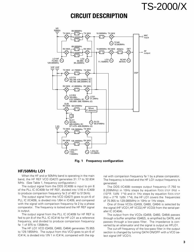
Frequency Configuration (Fig. 1)This transceiver utilizes double conversion in FM mode
and triple conversion in non-FM modes during transmission.It utilizes triple conversion in FM mode and quadruple
conversion in non-FM modes during reception. The fourth12kHz IF signal is converted from analog to digital and con-nected to the DSP.
When the carrier point frequency of the signal input fromthe antenna is fIN, the relationship between these signalswhen demodulating this signal is expressed by the followingequations:
HF MAIN fIN = fLO1 – fLO2 – fLO3 + fLO4 – 12kHzVHF MAIN fIN = fLO1 – fLO2 – fLO3 + fLO4 – 12kHzUHF MAIN fIN = fLO1 + fLO2 + fLO3 – fLO4 + 12kHz1.2G MAIN fIN = fLO1 x 2 + fLO2 + fLO3 – fLO4 + 12kHz
Reference Signal Generation CircuitThe 15.6MHz reference frequency fstd for PLL frequency
control is generated by the TCXO (X400). The signal passesthrough a buffer amplifier (Q420) and is used as the refer-ence signal for the second local oscillator (HFLO2) for HFband reception and the first local oscillator (SLO1) subbandreception.
The reference signal is doubled by Q412, and the result-ing 31.2MHz signal is used as the reference signal for DDSs(IC406, IC407, IC408, IC601, IC602, IC603).
The 31.2MHz signal is supplied to the TX-RX2 unit (X57-606 A/11) as LO2 for VHF and UHF bands.
CIRCUIT DESCRIPTION
3
TS-2000/X
68.985MHz
75.825MHz
TX MIX
TX MIX TX MIX
TX MIX TX MIX
69.085MHz10.695MHz
10.595MHz
75.925MHz
RX MIX RX MIX RX MIX DET
TCAR10.583MHz
455kHz
LO311.150MHz
LO1HF75.955~
129.085MHz
LO258.390~
65.230MHz
RCAR467kHz
41.795MHz
LO1TX183.795~418.205MHz (K)185.795~398.205MHz (E)
RX MIX RX MIX41.895MHz
SUBRX MIX 58.525MHz
LO1RX183.895~418.105MHz (K)185.895~398.105MHz (E)
SLO258.070MHz
TX MIX TX MIX135.395MHz
RX MIX RX MIX135.495MHz
1.2GLO11104~1165MHz
LO3131.2MHz
MixerIF detector
÷2
SLO1322.95~465.04MHz (K)371.475~409.050MHz (E)
HF/50MHz
UHFVHF
1.2G
1.2GLO2124.8MHz
DSP
MICinput
AFoutput
HF/50MHz LO1When the HF and or 50MHz band is operating in the main
band, the HF REF VCO (Q427) generates 31.17 to 32.834MHz. (See Table 1, frequency configuration.)
The output signal from the DDS (IC408) is input to pin 8of the PLL IC (IC409) for HF REF, divided into 1/16 in IC409to produce comparison frequency fø 2 of 487 to 513kHz.
The output signal from the VCO (Q427) goes to pin 6 ofPLL IC (IC409), is divided into 1/64 in IC409, and comparedwith the signal with comparison frequency fø 2 by a phasecomparator. The frequency is locked and the HF REF signalis output.
The output signal from the PLL IC (IC409) for HF REF isfed to pin 8 of the PLL IC (IC414) for HF LO1 as a referencefrequency, and divided to produce comparison frequencyfø 1 of 975 to 1358kHz.
The HF LO1 VCO (Q459, Q460, Q464) generates 75.955to 129.185MHz. The output from this VCO goes to pin 6 ofIC414, is divided into 1/N 1 in IC414, compared with the sig-
nal with comparison frequency fø 1 by a phase comparator.The frequency is locked and the HF LO1 output frequency isgenerated.
The DDS (IC408) sweeps output frequency (7.792 to8.209MHz) in 10Hz steps by equation fDDS STEP (Hz) =(10*R 1)/(N 1*4) and in 1Hz steps by equation fDDS STEP
(Hz) = (1*R 1)/(N 1*4), the HF LO1 covers the frequenciesof 75.955 to 129.085MHz in 10Hz or 1Hz steps.
One of three VCOs (Q459, Q460, Q464) is selected bythe signal (HF VCO1,HF VCO2,HF VCO3) from the serial-par-allel IC (IC404).
The output from the VCOs (Q459, Q460, Q464) passesthrough a buffer amplifier (Q462), is amplified by Q476, andpasses through a low-pass filter. The impedance is con-verted by an attenuator and the signal is output as HFLO1.
The cut-off frequency of the low-pass filter in the outputsection is changed by turning Q474 ON/OFF with a VCO se-lect signal (HF VCO1).
Fig. 1 Frequency configuration
CIRCUIT DESCRIPTION

4
TS-2000/X
HF LO2When the HF and or 50MHz band is operating, the
HF LO2 VCO (Q409) generates 65.230 to 58.390MHz. (SeeTable 1, frequency configuration.)
The 15.6MHz reference signal fstd is input to pin 8 of thePLL IC (IC401) for HF LO2, divided into 1/226 and 1/319 inIC401 to produce comparison frequency fø of 69.027 to48.903kHz.
The output signal from the VCO (Q409) goes to pin 6 ofIC401, its frequency is divided into 1/945 and 1/1194 inIC401, compared with comparison frequency fø by a phase
Display frequency LO1 OUT IC414 : HF REF IC409 : DDS output (MHz)
fRX (MHz) (MHz) LMX2306TMX (MHz) LMX2306TMX IC408 : AD9835BRU
Start Stop R1 N1 N2 R2
0.030000 1.999999 LO1 32 76 HF REF 64 16 fDDS
2.000000 5.999999 = fRX + IF 30 75 =
(fRX + IF) *R1
=
HF REF *R2
6.000000 8.999999 32 84 N1 N2
9.000000 12.999999 30 75
13.000000 16.999999 32 84
17.000000 17.999999 32 92
18.000000 21.999999 30 90
22.000000 23.999999 32 100
24.000000 24.999999 32 92
25.000000 25.999999 30 90
26.000000 29.999999 24 78
30.000000 32.999999 32 100
33.000000 36.999999 30 97
37.000000 40.999999 32 115
41.000000 44.999999 32 119
45.000000 48.999999 30 115
49.000000 51.999999 30 113
52.000000 55.999999 30 115
56.000000 60.000000 32 127
LO2 OUT IC401 : IF
(MHz) LMX2306TMX
N3 R3 RX TX
65.230088 945 226 75.925088 75.825088
58.389969 1194 319 69.084968 68.984968
65.230088 945 226 75.925088 75.825088
58.389969 1194 319 69.084968 68.984968
65.230088 945 226 75.925088 75.825088
58.389969 1194 319 69.084968 68.984968
65.230088 945 226 75.925088 75.825088
58.389969 1194 319 69.084968 68.984968
comparator, and locked. The division ratio data comes fromthe control unit.
The output signal from the VCO (Q409) passes through abuffer amplifier (Q415), is amplified by Q421, and passesthrough a low-pass filter. The impedance is converted by anattenuator and the signal is output as HF LO2.
When the HF and or 50MHz band is not operating, Q403is turned OFF with the LO2SEL signal and HF LO2 VCO(Q409) stops operation.
Table 1 Main HF and 50MHz band frequency configuration
CIRCUIT DESCRIPTION

5
TS-2000/X
144MHz LO1When the VHF band is operating in the main band, the
VHF REF VCO (Q441) generates 36.057 to 37.288MHz (K),36.450 to 36.842MHz (E). (See Table 2, Frequency Configu-ration.)
The output signal from the DDS (IC406) is input to pin 8of the PLL IC (IC411) for VHF REF and divided into 1/16 inIC411 to produce comparison frequency fø 2 of 563 to583kHz (K), 569 to 576kHz (E).
The output signal from the VCO (Q441) goes to pin 6 ofIC411 and its frequency is divided into 1/64 in IC411, com-pared with the signal with comparison frequency fø 2 by aphase comparator, and is locked.
The VHF REF PLL output signal is fed to pin 8 of IC410 asa reference frequency, and divided into 1/30 in IC410 to pro-duce comparison frequency fø 1 of 1202 to 1243kHz (K),1215 to 1228kHz (E).
The VHF LO1 VCO (Q433) generates 183.895 to 193.895MHz (K), 185.795 to 187.895MHz (E) in receive mode and183.795 to 193.795MHz (K), 185.795 to 187.795MHz (E).
The VCO (Q433) output signal goes to pin 6 of IC410, andits frequency is divided into 1/N1 in IC410 and comparedwith comparison frequency fø 1 by a phase comparator. Thefrequency is locked and LO1 is generated.
The DDS (IC406) sweeps output frequency (9.014 to
Display frequency LO1 OUT IC410 : VHF REF IC411 : DDS output (MHz)
fRX (MHz) (MHz) LMX2306TMX (MHz) LMX2306TMX IC406 : AD9835BRU
Start Stop R1 N1 N2 R2
142.000000 (K) 146.999999 (K) LO1 30 153 VHF REF 64 16 fDDS
144.000000 (E) 146.000000 (E) = fRX + IF =
(fRX + IF) *R1
=
VHF REF *R2
147.000000 (K) 151.999999 (K) 156 N1 N2
IF = RX : 41.895TX : 41.795
9.321MHz (K), 9.112 to 9.210MHz (E)) in 10Hz steps byequation fDDS STEP (Hz) = (10*R1)/(N1*4) and in 1Hz stepsby equation fDDS STEP (Hz) =(1*R1)/(N1*4), the LO1 coversthe frequencies of 183.895 to 193.895 MHz (K), 185.895 to187.895MHz (E) in receive mode and 183.795 to193.795MHz (K), 185.795 to 187.795MHz (E) in transmitmode in 10Hz or 1Hz steps.
The PLL output signal is changed by the switching circuitof Q469 (receive) and Q470 (transmit) so that the outputamplifier and low-pass filter correspond to VHF band trans-mission and reception.
In receive mode, the signal is amplified by the broad-band amplifier (IC415), and passes through a low-pass filter.The impedance is converted by an attenuator and the signalis output to the RF unit (X57-606) as the first local oscillatorRXLO1.
In transmit mode, the signal is amplified by the broad-band amplifier (IC416), and passes through a low-pass filter.The impedance is converted by an attenuator and the signalis output to the RF unit (X57-606) as the first local oscillatorTXLO1.
When the VHF is not operating, Q436 is turned OFF witha signal from the serial-parallel IC (IC404) and VHF LO1 VCO(Q433) stops operation.
430MHz LO1When the UHF band is operating in the main band, the
UHF REF VCO (Q431) generates 378.105 to 418.105MHz(K), 388.105 to 398.105MHz (E) in receive mode and378.205 and 418.205MHz (K), 388.205 to 398.205MHz (E).(See Table 3, Frequency Configuration.)
The output signal (8.328 to 8.475MHz (K), 8.344 to8.469MHz (E)) from the DDS (IC407) passes through a ce-ramic filter (CF400), is input to pin 8 of the PLL IC (IC412) forUHF and divided into 1/16 in IC412 to produce comparisonfrequency fø of 520 to 530 kHz.
The output signal from the VCO (Q431) goes to pin 6 ofIC412 and its frequency is divided into 1/N in IC412, com-pared with comparison frequency fø by a phase comparator,and is locked.
The DDS (IC407) sweeps output frequency (8.328 to8.475MHz (K), 8.344 to 8.469MHz (E)) in 10Hz steps byequation fDDS STEP (Hz) = 10*R/N and in 1Hz steps by equa-tion fDDS STEP (Hz) = 1*R/N, the LO1 covers the frequenciesof 378.105 to 418.105MHz (K), 388.105 to 398.105MHz (E)
in receive mode and 378.205 to 418.205MHz (K), 388.205 to398.205MHz (E) in transmit mode in 10Hz or 1Hz steps.
The PLL output signal is changed by the switching circuitof Q471 (receive) and Q472 (transmit) so that the outputamplifier and low-pass filter correspond to UHF band trans-mission and reception.
In receive mode, the signal is amplified by the broad-band amplifier (IC415), and passes through a low-pass filter.The impedance is converted by an attenuator and the signalis output to the RF unit (X57-606) as the local oscillator sig-nal RXLO1.
In transmit mode, the signal is amplified by the broad-band amplifier (IC416), and passes through a low-pass filter.The impedance is converted by an attenuator and the signalis output to the RF unit (X57-606) as the local oscillator sig-nal TXLO1.
When the UHF is not operating, Q434 is turned OFF witha signal from the serial-parallel IC (IC404) and UHF VCO(Q431) stops operation.
Table 2 Main VHF band frequency configuration
CIRCUIT DESCRIPTION

6
TS-2000/X
Display frequency LO1 OUT IC412ÅF DDS output (MHz)
fRX (MHz) (MHz) LMX2306TMX IC407 : AD9835BRU
Start Stop R N
420.000000 (K) 425.999999 (K) LO1 16 726 fDDS
425.000000 (K) 431.499999 (K) = fRX – IF 736 =
fRX – IF *R
430.000000 (E) N
431.500000 (K,E) 435.499999 (K,E) 747
435.500000 (K,E) 439.499999 (K,E) 754
439.500000 (K,E) 443.499999 (K) 762
440.000000 (E)
443.500000 (K) 447.999999 (K) 770
448.000000 (K) 449.999999 (K) 778
IF = RX : 41.895TX : 41.795
Table 3 Main UHF band frequency configuration
SUB LO1When the sub band receiver is operating, the sub VCO
(Q406, Q407) generates 322.95 to 465.040MHz. (See Table4, frequency configuration.)
The 15.6MHz reference signal fstd is input to pin 8 of thePLL IC (IC402) for the sub VCO, divided into 1/R in IC402 toproduce comparison frequency fø of 5 and 6.25kHz. Thedivision ratio data comes from the control unit.
The output signal from the VCO (Q406, Q407) goes to pin6 of IC402, its frequency is divided into 1/N in IC402, com-pared with comparison frequency fø by a phase comparator,and locked.
Display frequency SLO1 OUT IC404 : IC402 : LMX2316TMX
fRX (MHz) (MHz) BU4094BCFV Step : 5,10,15,20,30 (kHz) Step : 6.25,12.5,25,50,100 (kHz)
13pin : Q6 12pin : Q7 11pin : Q8 R N R N
Start Stop (BSW2) (BSW1) (B LU SW) Formula Formula
118.00000 (K) 118.94500 (K) SLO1 L H L 3120N =
2 x (fRX + 58.525) 2496N =
2 x (fRX + 58.525)
118.95000 (K) 134.99500 (K) = (fRX + 58.525) *2 H L 0.005 0.00625
135.00000 (K) 154.49500 (K) L H H
144.00000 (E) 146.00000 (E)
154.50000 (K) 173.99500 (K) H L
220.00000 (K) 235.99500 (K) SLO1 L H LN =
2 x (fRX – 58.525)N =
2 x (fRX – 58.525)
236.00000 (K) 252.49500 (K) = (fRX – 58.525) *2 H L 0.005 0.00625
252.50000 (K) 271.54500 (K) L H H
271.55000 (K) 289.99375 (K) H L
290.00000 (K) 296.42000 (K) SLO1 L H LN =
fRX + 58.525N =
fRX + 58.525
296.42500 (K) 328.99500 (K) = fRX + 58.525 H L 0.005 0.00625
329.00000 (K) 367.52000 (K) L H H
367.52500 (K) 399.99500 (K) H L
400.00000 (K) 413.47000 (K) SLO1 L H LN =
fRX – 58.525N =
fRX – 58.525
413.47500 (K) 445.99500 (K) = fRX – 58.525 H L 0.005
0.00625
430.00000 (E) 440.00000 (E)
446.00000 (K) 484.57000 (K) L H H
484.57500 (K) 511.99500 (K) H L
The output signal from the VCO (Q406, Q407) passesthrough a buffer amplifier (Q413, Q414), is amplified by thebroad-band amplifier (IC405), and passes through a low-passfilter. The impedance is converted by an attenuator and thesignal is output as SLO1.
When the sub band receiver is not operating, Q411 andQ411 are turned OFF with the BSW1 and BSW2 signals andsub VCO (Q406, Q407) stops operation.
Table 4 Sub band frequency configuration
CIRCUIT DESCRIPTION

7
TS-2000/X
1.2GHz Unit Local OscillatorThe 12LO31 signal (31.2MHz) is quadrupled to 124.8MHz
in Q14 and 15. This signal is sent to the mixers of the trans-mitter section (Q1 and Q2) and the mixers of the receiversection (Q7 and Q8)
In the DDS (C4) , 8.323~8.488MHz are output using12LO31 as the reference signal. This signal passes througha filter (CF1 and CF2) and is input to the mixers for referencePLL signals (Q313 and 314).
In Q313 and Q314, the DDS output is mixed with12LO31 (31.2MHz) and an approximately 39.6MHz signal isobtained. This signal passes through a filter and an amplifier(Q312) and becomes the reference signal of the PLL IC(IC5).
The VCO (Q301) oscillates at 552.253~582.303MHz.This signal is amplified in Q302 and goes to the PLL IC (IC5)and Q19.
The PLL IC (IC5) divides the reference signal (approxi-mately 39.6MHz) to 1/72. The signal from Q302 is divided to1/N (N=1006~1058).
Display frequency Q301 oscillation C5 : DDS output (MHz)
fRF (MHz) frequency LMX2316TMX IC4 : AD9851BRS
Start Stop fVCO (MHz) R N
1240.000000 (K) 1243.999999 (K) fVCO 72 1006 fDDS
1244.000000 (K) 1245.999999 (K) = (fRF – IF)/2 1008=
(fRF – IF)*R – 31.2
1246.000000 (K) 1249.999999 (K) 1011 2*N
1250.000000 (K) 1253.999999 (K) 1015
1254.000000 (K) 1255.999999 (K) 1017
1256.000000 (K) 1258.999999 (K) 1020
1259.000000 (K) 1262.999999 1023
1260.000000 (E)
1263.000000 1266.999999 1027
1267.000000 1270.999999 1030
1271.000000 1274.999999 1034
1275.000000 1277.999999 1037
1278.000000 1280.999999 1040
1281.000000 1284.999999 1043
1285.000000 1288.999999 1047
1289.000000 1292.499999 1050
1292.500000 1294.999999 1053
1295.000000 1297.999999 1056
1298.000000 1299.999999 1058
The two signals are compared in the phase comparatorwithin the IC and the VCO (Q301) oscillation frequency islocked.
The signal input into Q19 is doubled. This signal passesthrough a filter and an amplifier (Q20) and goes to the send-ing mixer (D1) and the receiving mixer (Q10).
Table 5 1.2GHz band frequency configuration
Local SignalsThe RXLO3 (11.15MHz) and RCAR (467kHz) for reception
and TCAR (10.583MHz) for transmission are output fromDDSs (RXL03 : IC603, RCAR : IC601, TCAR : IC602).
The frequencies of local oscillator output signals (LO1,LO2, RCAR, TCAR) for each band are shifted by offset (IFfilter setting), RIT, XIT, IF SHIFT as listed in Tables 5 to 11.
Fig. 2 1.2GHz unit local oscillator
L52Q20Q19 Q312 Q16 Q13
Q313,314 39.523~
39.688MHzQ302
Q301
1104~1165MHz
L340~342
39.6MHz
8.323~8.488MHz
CF1,2
8.4MHz
IC5 IC14
PLL DDS
552.253~582.303MHz
Q310,311
Q10
D1
TX-RX 3 (X57-607)
D10
D11
RX
TX
L42,43Q15 Q14
124.8MHz
Q7,8RX
Q1,2TX
D8
31.2MHz
31.2MHz
Q65LO31
31.2MHz12LO31
X57-606
IF=RX : 135.495TX : 135.395
CIRCUIT DESCRIPTION

8
TS-2000/X
DDS IC408 : AD9835BRU
HF TX/RX LO1 LSB USB CW CW-R
RX TX RX TX RX TX RX TX
Filter offset –1.5k –1.5k +1.5k +1.5k +0.7k +0.7k –0.7k –0.7k
RIT +(D RIT) – +(D RIT) – +(D RIT) – +(D RIT) –
XIT – +(D XIT) – +(D XIT) – +(D XIT) – +(D XIT)
SLOPE H +(SSB H) – –(SSB H) – –(CW H) – +(CW H) –
10.695MHz Filter Adj. +(D 10.695) – –(D 10.695) – – – – –
HF TX/RX LO1 FSK FSK-R AM FM
RX TX RX TX RX TX RX TX
Filter offset –(1.5k–Fcenter) 0 +(1.5k–Fcenter) 0 0 0 0 0
RIT +(D XIT) – +(D RIT) – +(D RIT) – +(D RIT) –
XIT – +(D XIT) – +(D XIT) – +(D XIT) – +(D XIT)
SLOPE H +(FSK H) – –(FSK H) – – – – –
10.695MHz Filter Adj. – – – – – – – –
DDS IC406 : AD9835BRU
144MHz TX/RX LO1 LSB USB CW CW-R
RX TX RX TX RX TX RX TX
Filter offset –1.5k –1.5k +1.5k +1.5k +0.7k +0.7k –0.7k –0.7k
RIT +(D RIT) – +(D RIT) – +(D RIT) – +(D RIT) –
XIT – +(D XIT) – +(D XIT) – +(D XIT) – +(D XIT)
SLOPE H +(SSB H) – –(SSB H) – –(CW H) – +(CW H) –
10.695MHz Filter Adj. +(D 10.695) – –(D 10.695) – – – – –
144MHz TX/RX LO1 FSK FSK-R AM FM
RX TX RX TX RX TX RX TX
Filter offset –(1.5k–Fcenter) 0 +(1.5k–Fcenter) 0 0 0 0 0
RIT +(D XIT) – +(D RIT) – +(D RIT) – +(D RIT) –
XIT – +(D XIT) – +(D XIT) – +(D XIT) – +(D XIT)
SLOPE H +(FSK H) – –(FSK H) – – – – –
10.695MHz Filter Adj. – – – – – – – –
DDS IC407 : AD9835BRU
430MHz TX/RX LO1 LSB USB CW CW-R
RX TX RX TX RX TX RX TX
Filter offset –1.5k –1.5k +1.5k +1.5k +0.7k +0.7k –0.7k –0.7k
RIT +(D RIT) – +(D RIT) – +(D RIT) – +(D RIT) –
XIT – +(D XIT) – +(D XIT) – +(D XIT) – +(D XIT)
SLOPE H +(SSB H) – –(SSB H) – –(CW H) – +(CW H) –
10.695MHz Filter Adj. +(D 10.695) – –(D 10.695) – – – – –
430MHz TX/RX LO1 FSK FSK-R AM FM
RX TX RX TX RX TX RX TX
Filter offset –(1.5k–Fcenter) 0 +(1.5k–Fcenter) 0 0 0 0 0
RIT +(D XIT) – +(D RIT) – +(D RIT) – +(D RIT) –
XIT – +(D XIT) – +(D XIT) – +(D XIT) – +(D XIT)
SLOPE H +(FSK H) – –(FSK H) – – – – –
10.695MHz Filter Adj. – – – – – – – –
Table 6 HF band LO1 frequency shift data
Table 7 144MHz band LO1 frequency shift data
Table 8 430MHz band LO1 frequency shift data
CIRCUIT DESCRIPTION

9
TS-2000/X
DDS IC4 : AD9851BRS
1.2GHz TX/RX LO1 LSB USB CW CW-R
RX TX RX TX RX TX RX TX
Filter offset –1.5k –1.5k +1.5k +1.5k +0.7k +0.7k –0.7k –0.7k
RIT +(D RIT) – +(D RIT) – +(D RIT) – +(D RIT) –
XIT – +(D XIT) – +(D XIT) – +(D XIT) – +(D XIT)
SLOPE H +(SSB H) – –(SSB H) – –(CW H) – +(CW H) –
10.695MHz Filter Adj. +(D 10.695) – –(D 10.695) – – – – –
1.2GHz TX/RX LO1 FSK FSK-R AM FM
RX TX RX TX RX TX RX TX
Filter offset –(1.5k–Fcenter) 0 +(1.5k–Fcenter) 0 0 0 0 0
RIT +(D XIT) – +(D RIT) – +(D RIT) – +(D RIT) –
XIT – +(D XIT) – +(D XIT) – +(D XIT) – +(D XIT)
SLOPE H +(FSK H) – –(FSK H) – – – – –
10.695MHz Filter Adj. – – – – – – – –
RX LO3 DDS IC603 : AD9835BRU
LSB USB CW CW-R FSK FSK-R AM FM
BASE 11.150 (MHz)
HF SLOPE H +(SSB H) –(SSB H) –(CW H) +(CW H) +(FSK H) –(FSK H) – –
SLOPE L +(SSB L) –(SSB L) –(CW L) +(CW L) +(FSK L) –(FSK L) – –
10.695MHz Filter Adj. +(D 10.695) –(D 10.695) – – – – – –
455kHz Filter Adj. +(D 455) –(D 455) – – – – – –
144 SLOPE H +(SSB H) –(SSB H) –(CW H) +(CW H) +(FSK H) –(FSK H) – –
MHz SLOPE L +(SSB L) –(SSB L) –(CW L) +(CW L) +(FSK L) –(FSK L) – –
10.695MHz Filter Adj. +(D 10.695) –(D 10.695) – – – – – –
455kHz Filter Adj. +(D 455) –(D 455) – – – – – –
430 SLOPE H –(SSB H) +(SSB H) +(CW H) –(CW H) –(FSK H) +(FSK H) – –
MHz SLOPE L –(SSB L) +(SSB L) +(CW L) –(CW L) –(FSK L) +(FSK L) – –
10.695MHz Filter Adj. –(D 10.695) +(D 10.695) – – – – – –
455kHz Filter Adj. –(D 455) +(D 455) – – – – – –
1.2 SLOPE H –(SSB H) +(SSB H) +(CW H) –(CW H) –(FSK H) +(FSK H) – –
GHz SLOPE L –(SSB L) +(SSB L) +(CW L) –(CW L) –(FSK L) +(FSK L) – –
10.695MHz Filter Adj. –(D 10.695) +(D 10.695) – – – – – –
455kHz Filter Adj. –(D 455) +(D 455) – – – – – –
Table 9 1.2GHz band LO1 frequency shift data
Table 10 RX LO3 frequency shift data
CIRCUIT DESCRIPTION

10
TS-2000/X
RCAR DDS IC601 : AD9835BRU
LSB USB CW CW-R FSK FSK-R AM FM
BASE 467 (kHz)
HF Filter offset +1.5k –1.5k –0.7k +0.7k +(1.5k–Fcenter) –(1.5k–Fcenter) 0 0
CW pitch – – –(PITCH) +(PITCH) – – – –
FSK tone H – – – – +2.125k –2.125k–FSK SHIFT – –
FSK tone L – – – – +1.275k –1.275k–FSK SHIFT – –
SLOPE L +(SSB L) –(SSB L) –(CW L) +(CW L) +(FSK L) –(FSK L) – –
455kHz Filter Adj. +(D 455) –(D 455) – – – – – –
144 Filter offset +1.5k –1.5k –0.7k +0.7k +(1.5k–Fcenter) –(1.5k–Fcenter) 0 0
MHz CW pitch – – –(PITCH) +(PITCH) – – – –
FSK tone H – – – – +2.125k –2.125k–FSK SHIFT – –
FSK tone L – – – – +1.275k –1.275k–FSK SHIFT – –
SLOPE L +(SSB L) –(SSB L) –(CW L) +(CW L) +(FSK L) –(FSK L) – –
455kHz Filter Adj. +(D 455) –(D 455) – – – – – –
430 Filter offset –1.5k +1.5k +0.7k –0.7k –(1.5k–Fcenter) +(1.5k–Fcenter) 0 0
MHz CW pitch – – +(PITCH) –(PITCH) – – – –
FSK tone H – – – – –2.125k +2.125k+FSK SHIFT – –
FSK tone L – – – – –1.275k +1.275k+FSK SHIFT – –
SLOPE L –(SSB L) +(SSB L) +(CW L) –(CW L) –(FSK L) +(FSK L) – –
455kHz Filter Adj. –(D 455) +(D 455) – – – – – –
1.2 Filter offset –1.5k +1.5k +0.7k –0.7k –(1.5k–Fcenter) +(1.5k–Fcenter) 0 0
GHz CW pitch – – +(PITCH) –(PITCH) – – – –
FSK tone H – – – – –2.125k +2.125k+FSK SHIFT – –
FSK tone L – – – – –1.275k +1.275k+FSK SHIFT – –
SLOPE L –(SSB L) +(SSB L) +(CW L) –(CW L) –(FSK L) +(FSK L) – –
455kHz Filter Adj. –(D 455) +(D 455) – – – – – –
TCAR DDS IC602 : AD9835BRU
LSB USB CW CW-R FSK FSK-R AM FM
BASE 10.583 (MHz)
HF Filter offset –1.5k +1.5k +0.7k –0.7k 0 0 0 0
144MHz Filter offset –1.5k +1.5k +0.7k –0.7k 0 0 0 0
430MHz Filter offset +1.5k –1.5k –0.7k +0.7k 0 0 0 0
1.2GHz Filter offset +1.5k –1.5k –0.7k +0.7k 0 0 0 0
Description of variables in Tables 6 to 12(D RIT) RIT frequency variable amount (–9.99~+9.99kHz)(D XIT) XIT frequency variable amount (–9.99~+9.99kHz)(SSB H) SSB slope high cut frequency variable amount = 2.8k – Fhi(SSB L) SSB slope low cut frequency variable amount = Flow – 300(CW H) CW slope high cut frequency variable amount = 2.7k – (FSK SHIFT + Fwidth / 2)(CW L) CW slope low cut frequency variable amount = FSK SHIFT – Fwidth / 2 – 100(FSK H) FSK slope high cut frequency variable amount = 2.8k – (Fcenter + Fwidth / 2)(FSK L) FSK slope low cut frequency variable amount = Fcenter – Fwidth / 2(D 10.695) RX 10.695MHz filter adjustment frequency variable amount(D 455) RX 455kHz filter adjustment frequency variable amount(PITCH) CW pitch frequency (400~1000Hz, Initial value 800Hz)(FSK SHIFT) FSK shift width frequency (170Hz, 200Hz, 425Hz, 850Hz, Initial value 170Hz)(Fcenter) FSK RX center frequency = (2125Hz or 1275Hz) + (FSK SHIFT / 2)
Table 11 RCAR frequency shift data
Table 12 TCAR frequency shift data
CIRCUIT DESCRIPTION

11
TS-2000/X
HF Receiver System and Main IF SystemThree antenna terminals used for the HF and 50MHz
band reception are ANT1, ANT2 and HF RX ANT.After the incoming signal from ANT1 and ANT2 passes
through the transmission/reception changeover relay in thefilter unit (X51-315), and is sent to the HFRX terminal of theTX-RX unit (X57-605). There is an HF RX ANT terminal there,and one of the antennas can be selected from the menu forreception .
The HF RX ANT terminal is used to connect a dedicatedHF-band low-band receiving antenna, such as a Beverageantenna, and operates at frequencies up to 30MHz. (If anantenna, such as a solid wire antenna, is connected to thisterminal, unwanted radio signals in the shack may be pickedup. It is recommended that a 50 (coaxial cable be used forrouting in the shack.)
The signal passes through an RF ATT, an image filter anda limiter for surge absorption and enters the RF BPF for bothtransmission and reception. The division of the RF BPF is inthe range shown in the block diagram. For 6.9~7.5MHz,13.9~14.5MHz and 49~54MHz, a dedicated BPF (adjustabletype) is used and particularly effective for eliminating un-wanted signals in the low band. Other BPFs (non-adjustabletype) are designed as circuits with independent armaturebands, except that the 24MHz and 28MHz bands areshared. Signals pass through these BPFs at the time oftransmission, so they are useful for producing radio signalswith little radiation.
Although the conventional RF ATT had an attenuationlevel of 20dB, the attenuation level of the current RF ATT is12dB. It can, however, be changed to approximately 20dBby removing the jumper (CN2) near the ATT within the unit.
The pre-amplifier (Q12, Q705) have been changed to apower MOS FET from the combination of the conventionalcascade amplifier and MOS FET amplifier. This element is aFET that is used in a younger stage for transmission and has
excellent large input characteristics. The actual circuit con-tains two amplifiers using this FET. Large input characteris-tics with a low gain are given priority on the low band (Q12)with respect to 21.5MHz, and sensitivity is given priority onthe high band (Q705). circuit on the low band side bordering21.5 MHz favoring a gain with moderately large input char-acteristics and that on the hybrid side (Q705) favoring .When the pre-amplifier is off, the signal from the RF BPFenters the receiving first mixer (Q7~Q10) in the next stageas it is.
The receiving first mixer circuit uses a double balancetype mixer with four joint type FETs. The signal is convertedto the first IF frequency by the first local oscillator signal.The TS-2000S has adopted a method that changes the firstIF frequency according to the receive frequency. For thisreason, it has two sets of roofing filters (MCF) that deter-mine the selectivity of the first IF. Table 1 shows the rela-tionship between the receive frequency and the first IF fre-quency. The central frequencies for the reception andtransmission of the first IF frequency are different from eachother by 100kHz because the transmission and reception isperformed simultaneously during satellite communication.
–12dB
ATT
LPF
L1
TX-RX 1 (X57-605 A/9)
HPF BPF
1.705~2.5MHz
49.0~54.0MHz
D12 D13
BPFD33 D34
30kHz~1.705MHz
1.705MHz~60MHz
D7 D8 D10
D11
RF BPF
D38D39
D705 D704
PRE AMPQ12
30kHz~21.5MHz
ANT1 ANT2 HF RX ANT
Q70521.5MHz~60MHz
D35D36
1st MixerQ7~Q10
XF169.085MHz
XF275.925MHz
X51-315FILTER
X57-605TX-RX1
Q18
2nd MixerQ19,Q20
D42 D41
10.695MHz
Q13
LO1HF75.955~
129.085MHz
RX/TX frequency (MHz) RX 1st IF (MHz) TX 1st IF (MHz)
0.03~ 9.0 75.925 75.825
9.0 ~17.0 69.085 68.985
17.0 ~24.0 75.925 75.825
24.0 ~26.0 69.085 68.985
26.0 ~30.0 75.925 75.825
30.0 ~37.0 69.085 68.985
37.0 ~49.0 75.925 75.825
49.0 ~60.0 69.085 68.985
Table 13 RX frequency and 1st IF frequency
Fig. 3
CIRCUIT DESCRIPTION

12
TS-2000/X
The signal is then amplified by the first IF amplifier (Q18)and is converted to the second IF frequency of 10.695MHzin the second receive mixers (Q19, 20). The tuning fre-quency of each stage, the second local oscillator frequencyand others are changed according to the receive frequencyto respond to the changeover of the previously stated first IFfrequency.
A circuit for changing over the IF signal from the units ofthe VHF, UHF and 1.2GHz bands and IF signal from the HFband is provided on the output side of the second receivemixer. That is, the circuits following this stage are com-monly used circuits, regardless of the receive frequency onthe main side.
In addition, there is a semi-fixed volume (VR4) on the out-put side of the first receive mixer. The volume is used toeliminate the gain differential generated due to thechangeover of the first IF frequency.
The signal for the noise blanker is extracted from thispoint by passing through Q22. The noise blanker circuit isbased on the same principle of operation as the conven-tional one, but can change the threshold level by changingthe emitter potential of the noise detection stage (Q29).
The 10.695MHz signal is amplified by Q26 which alsoserves as a noise blanker gate circuit and passes through a10.695MHz IF filter. It has three bandwidths, 2.7kHz, 6kHzand through, and when it is combined with the 455kHz filtergroup, the same continuous band change function (analog IFthroughput: operation in modes other than FM) as in con-
ventional analog devices is implemented. The band in thisanalog stage does not affect the operation of the digital IFfilter in the IF DSP and is automatically set to the optimumband for removing unwanted signals outside the band.
Then, the signal is converted to the third IF frequency of455kHz in the third receive mixer (Q700, 701). The 455kHzfilter has three bandwidths: 2.7kHz, 9kHz and 15kHz. In FMmode (main band side) the 15kHz filter is selected for WIDEand the 9kHz filter is selected for NARROW, and signalspassing through the filter are sent to the FM IC (ICI), ampli-fied and detected. IC1 processes squelch, S meter, etc.
As a characteristic operation in this stage, a tuning errordetection voltage for the ALT function operating in the1.2GHz band FM mode is generated. It utilizes the DC volt-age that is overlapped with the ICI detection output.
In a mode other than FM, the receive signal is amplifiedby the next third IF amplifier (Q38) and operational amplifier(IC18) and converted to the final 12kHz IF frequency by thefourth receive mixer (IC3). The converted IF signal in FM(audio signal) and non-FM mode (IF signal) is selected by themultiplexer (IC7) and the signal is sent to the DSP of thecontrol unit for processing. The signals processed in thecontrol unit become audio signals in all modes and return tothe TX-RX1 unit (X57-605). These audio signals are poweramplified to the level that drives the speaker with the AMamplifier (IC9).
A speaker separation function is available as an acces-sory circuit. The bands can be changed as shown in Table14.
D71 D70Q32
LO311.15MHz
2nd MixerQ19,20
Q1810.695MHz
D46
D47
X57-606RIF
X57-60712RIF
Q22 Q26 Q28
Q25
SW
Q29~Q31
Noise blanker
LO265.230MHz58.390MHz
D60,64 D52,56
D49,55 D57,61
D58,62D50,53
XF5
XF6
10.695MHz
3rd MixerQ700,701
Q41
RCAR467kHz
4th MixerIC3
CF1D69 D67
CF2
CF3
FMDETALT
AF
FMFM IC
D68
Q38
IC18IC2
TX-RX 1 (X57-605 A/9)
IC1
CF4455kHz
Q709 Q42
12kHzDSP
AF PA AMPIC9
X53-391
Fig. 4
CIRCUIT DESCRIPTION

13
TS-2000/X
Speaker output changeover
When external speakers 1 and 2 and headphones areconnected, you can change over the sub/main band outputs.
The headphone connection is preferred over the all thespeaker output and you can select from three patterns forheadphone left-right changeover.
Connection Conditions ( : connected) Output condition by connection of left table
Headphone SP1 SP2 Headphone Built-in speaker SP1 SP2
X X → Pattern 0~2 Stop X X
X → Pattern 0~2 Stop Stop X
→ Pattern 0~2 Stop Stop Stop
X → Pattern 0~2 Stop X Stop
X → X Stop Pattern 0~2 (Left) Pattern 0~2 (Right)
X X → X Pattern 0~2 (Left) X Pattern 0~2 (Right)
X X → X Stop Main-sub full mix X
X X X → X Main-sub full mix X X
Left-right output patterns
In case of headphones In case of SP1 & SP2
Selected Pattern Left side Right side SP1 or Built-in SP2
Pattern 0 Main-sub full mox Main-sub full mix Main-sub full mix Main-sub full mix
Pattern 1 Main : Full sound Main : 1/4 sound main : Full sound Main : 1/4 sound
Sub : 1/4 sound Sub : Full sound Sub : 1/4 sound Sub : Full sound
Pattern 2 Main Sub main Sub
This is a reverse function and left-right changeover is possible.
When SP1 only has been connected, the built-in speakerwill change over to SP1.
When SP1 and SP2 are connected, you can select theSP1 and SP2 output method from three patterns, the sameas for the headphones.
Table 14
Main VHF/UHF Band Front-End and
Sub Receiver SystemThe VHF and UHF band receiver circuit is configured with
two systems, a main band (FM/ AM/ SSB/ CW/ FSK) and asub-band (FM/AM), each of which has a VHF and a UHFband path.
In the main band, the first IF is 41.895MHz and the sec-ond IF is 10.695MHz and the signal lower hetero to the sec-ond IF is sent to the TX-RX1 unit (X57-605) and linked to thesecond IF, which is shared by the other bands. The sub-band is a double conversion where the first IF is 58.525MHzand the second IF is 455kHz. It is configured so that de-tected AF signals are sent to the control unit (X53-391).
VHF/ UHF band front end
The circuit operation of the sub-receiver unit differs de-pending on whether it is for K destination or others. Thecircuit operation for each of the destinations is describedbelow.
• K destination
The incoming signal from the VHF band antenna terminalpasses through the TX/RX changeover relay (K2) in the filterunit (X51-315) and goes to the TX-RX2 unit (X57-606). Then,it passes through the 12dB ATT circuit and is divided to the136~155MHz path and the 118~136MHz, 155~174MHzand 220~300MHz path by the L distribution circuit. The136~155MHz signal passes through a 2-pole BPF (band-pass filter) and enters the pre-amplifier (Q15). The ampli-fied receive signal is again distributed to the paths for themain and sub receiver units by the L distribution circuit.
The signal distributed to the main receiver unit passesthrough the 2-pole variable tuning BPF, is amplified by thesecond amplifier (Q24) and goes to the mixer (IC4) for themain band common to the VHF and UHF bands through thevariable tuning BPF. The 2-pole x 2-stage BPF for the mainband VHF controls the tuning frequency by output from theD/A of the TX-RX1 unit (X57-605).
CIRCUIT DESCRIPTION

14
TS-2000/X
The 118~174MHz signal distributed to the sub-receiverunit passes through a variable tuning filter and is amplifiedby the second amplifier (Q24). Then, it passes through the2-pole variable tuning BPF, and the 220~300 MHz signal isamplified by Q23 and is then input into the mixer (IC5) forthe sub-band common to the VHF and UHF bands. The 1-pole and 2-pole BPFs for the sub-band VHF also controls thetuning frequency by the output from the D/A of the TX-RX1unit (X57-605).
The incoming signal from the UHF band antenna terminalenters the UHF section of the final unit (X45-360), passesthrough the HPF and LPF and goes to the TX-RX2 unit (X57-605). Then, it passes through the 12dB ATT circuit and goesto the pre-amplifier (Q14). The amplified receive signal isdistributed to the paths of the main and sub-receiver sec-tions by the L distribution circuit.
The signal distributed to the main receiver sectionpasses through the 3-pole variable tuning BPF and is ampli-fied by the second amplifier (Q21). Then, it passes throughthe 3-pole variable tuning BPF and is input into the mixer(IC4) for the main band.
This 3-pole x 2 stage BPF for the UHF also controls thetuning frequency by the output from the D/A of the TX-RX1unit (X57-605).
The 438~450MHz signal distributed to the sub-receiversection passes through the SAW filter (L29), is amplified bythe second amplifier (Q25), and passes through anotherSAW filter (L50). The 300~438MHz and 450~512MHz sig-nals are amplified by Q19 and goes to the mixer (IC5) for thesub-band.
• E, E2 destinations
Then, the signal passes through the 12dB ATT circuit andthe 2-pole BPF (band-pass filter) and enters the pre-amplifier(Q15). The amplified receive signal is distributed to thepaths of the main and sub receiver sections by the L distri-bution circuit.
The signal distributed to the sub-receiver section passesthrough a variable tuning filter and is amplified by the sec-ond amplifier (Q22). Then, it passes through the 2-pole tun-ing BPF, and goes to the mixer (IC5) for the sub-band com-mon to the VHF and UHF bands. The 1-pole + 2-pole BPFsfor the sub-band VHF also control the tuning frequency bythe output from the D/A of the TX-RX1 unit (X57-605).
The signal distributed to the sub-receiver section passesthrough the SAW filter (L29), is amplified in the second am-plifier (Q25), passes through another SAW filter (L50) andgoes to the mixer (IC5) for the sub-band.
Q44
LO3131.200MHz
Q42,43
–12dB
ATT
D10 D24 D48D22
Q15 Q24
Q38
Q30
Q61
L23,24 L47,55
–12dB
ATT D9
TX-RX 2 (X57-606 A/11)
D49D23Q14 Q21
L108~111,137 L116~119,133
XF141.895MHzIC4LO1RX
183.895~418.105MHz
VHF
UHF
FilterX51-315
FinalX45-360
RIF
RIF
D46
Q22
X57-605
–12dB
ATT D10 D95
D24
D46D22Q15 Q22
D96
D97
D101 L28
L29
L44,52
L50
VHF
FilterX51-315
D23
D82Q23
D90 D91Q25
D94D93Q19–12dB
ATT D9
TX-RX 2 (X57-606 A/11)
D92 D81D20Q14
UHF
FinalX45-360
IC5
Fig. 5 Main band receiver section
Fig. 6 Sub band receiver section
CIRCUIT DESCRIPTION

15
TS-2000/X
Main receiver IF section
The signal input to IC4 is mixed with the signal producedby amplifying the first local oscillator RXLO1 from the PLLsection by Q30 and lower hetero to the first IF of41.895MHz. Then, it passes through the MCF (XF1) andAGC amplifier (Q38) and goes to the second mixer (Q42 and43). The signal input to the second mixer is mixed with thesignal produced by amplifying the second local oscillator21.2MHz from the PLL section by Q44 and lower hetero tothe second IF of 19.695MHz. The signal then passesthrough a temperature compensating resistor and the IFamplifier (Q61) and is sent to the TX-RX1 unit (X57-605).
Sub receiver IF section
The signal input to IC5 is lower hetero to the first IF of58.525MHz. In the VHF band, the local oscillator SLO1 fromthe PLL section is divided into two by the divider (IC6) andpasses through amplifier (Q23). In the UHF band, the IF sig-nal passes through amplifier (Q33) and is input to IC5. TheIF signal passes through the MCF (XF2), passes through thepost amplifier (AGC amplifier in the AM mode) Q37 andgoes to the FM IC (IC7). The local oscillator is supplied toIC7 by the 58.07MHz crystal oscillator (X1) and is lowerhetero to the second IF of 455kHz by a mixer in the IC.
The circuit operation when the signal passes through aceramic filter after lower hetero is different for K destinationand E destination. The circuit operation for each of the des-tinations is explained below.
CF2 (E type only)
CF1
455kHz
DSP
IC6IC9
X53-391
FM
58.07MHz
Q51 Q48 Q45
Q39
D58AM
FM ICIC7
Q37
XF258.525MHz
IC5
AGC
D53 D56Q32
Q33 TX-RX 2 (X57-606 A/11)
IC6
1/2VHF
UHF
SLO1322.95~465.04MHz
176.5~231.5MHz
348.5~458.5MHz
SQ
Q63 D83
S-meter
Q44
LO3131.2MHz
Q42,43
Q38
Q30 Q61XF1
41.895MHzIC4
LO1RX
RIF
X57-605
VHF
UHF
TX-RX 2 (X57-6060 A/11)
D46
D49
HF 1.2GHz
Q22
10.695MHz
• K destination
In FM mode, the signal passes through a ceramic filter(CF1), is quadrature-detected, and the resulting signal is out-put.
• E, E2 destinations
The signal passes through a ceramic filter (CF1) in FMWIDE mode and it passes through a ceramic filter (CF2) inFM NARROW mode. The signal is then quadrature-de-tected and the resulting signal is output.
In AM mode, a 455kHz signal passes through the AGCamplifier (Q51) and amplifier (Q48 and Q45) and is detectedby D58. The detection signal retrieved for the AGC is recti-fied, passes through the DC amplifier (Q39) for AGC controland goes to the Q37 gate terminal (G2).
The FM/AM detection signal is switched by the multi-plexer (IC8). Then, it is amplified by the operational amplifier(IC9) and output to the control unit (X53-391).
Squelch voltage and S-meter voltage of the sub
receiver section
The S meter voltage is introduced to the A/D through aLPF for RSSI output of the FM IC (IC7).
The squelch voltage is supplied to the A/D by passing thedetection output of the FM IC through a filter amplifier in theFM IC, amplifying it with the noise amplifier (Q63), and recti-fying it with D83.
Fig. 7
Fig. 8
CIRCUIT DESCRIPTION

16
TS-2000/X
1.2GHz Unit Receiver SectionThe incoming signal from the antenna (12ANT) passes
through a filter, is amplified in the receiver RF amplifier (Q11and 12) and input to the first mixer (Q10).
The signal is converted to the first IF (135.495MHz) inQ10, passes through the MCF (XF1) and the AGC amplifier(Q9) and enters the second mixer (Q7 and Q8).
The signal is converted to the second IF (10.695MHz) inQ7 and Q8, amplified in the receiver IF amplifier (Q303) andsent to the TX-RX1 unit (X57-605).
D5
D6,
7,30
3
TX
TX/RX SW Q12 Q11L33 L30
1240~1300MHz
1st MixerQ10
2nd MixerQ7,8XF1
135.495MHz
Q9 Q303
AGCCN12
CN11
D11
1104~1165MHz
124.800MHz
Q15
TX-RX 3 (X57-607)
D810.695
MHz
D4712RIF
X57-605
12ANT
Ref No. XF1 XF2 XF3 CF1 CF2
Parts No. L71-0566-05 L71-0565-05 L71-0582-05 L72-0984-05 L72-0986-05
Nominal center frequency 41.895MHz 58.525MHz 41.795MHz 455kHz 455kHz
Pass bandwidth 3dB : ±7.5kHz 3dB : ±7.5kHz 3dB : ±15kHz 6dB : ±7.5kHz or more 6dB : ±4.5kHz or more
50dB : ± 15kHz or less 50dB : ± 10kHz or less
Ripple 1.0dB or less 1.0dB or less 1.0dB or less 2.0dB or less 2.0dB or less
Insertion loss 3.0dB or less 3.5dB or less 1.5dB or less 6.0dB or less 6.0dB or less
Guaranteed attenuation Fo+(500~1000)kHz Fo±1MHz Fo–(500~1000)kHz Fo±100kHz Fo±100kHz
Fo–(200~1000)kHz 80dB or more 50dB or more 35dB or more 35dB or more
70dB or more
Cener – – – 455kHz±1.0kHz 455kHz±1.0kHz
Terminating impedance 960Ω//1.0pF 350Ω//4.0pF 960Ω//1.0pF 1.5kΩ 2.0kΩ
CC=7.0pF CC=15.5pF
Spurious Fo±1.0MHz Fo±1.0MHz – – –
40dB or more 40dB or more
CF2 : Only E destination
Table 15 Filters rating (TX-RX 2 unit : X57-606)
Fig. 9
CIRCUIT DESCRIPTION

17
TS-2000/X
Transmit System IF Section
Transmission IF
The details of the processing by the DSP depend on themode.
• Modes other than FM
Transmission bandwidth change, speech processor andmicrophone gain control are performed in the AF stage. A12kHz IF signal is produced after PSN modulation and out-put modulation control.
• FM mode
The baseband processing in the AF stage is carried out bythe DSP and a VCXO (voltage controlled X’tal Oscillator) isused as a modulator.
The transmit signal output from the control unit (X53-391)is switched by an analog SW (IC8) and is input to the bal-anced mixer (IC6). The 12kHz IF signal and local oscillatorsignal enters the IC6 and become a 10.595MHz signal. Thelocal oscillator signal is generated by the DDS (IC602).
The 10.595MHz IF component is amplified by the IF am-plifier (Q54) and passes through the 6kHz bandwidth crystalfilter, then becomes a 10.595MHz IF signal by eliminatinglocal oscillator signals. The diode switch (D90) changes be-tween FM modulator output and non-FM 10.595MHz IF sig-nals.
The temperature compensation of the transmitter circuitis done by the thermistor near the IF amplifier (Q54) and thethermistor on the input side of the IF amplifier (Q711). Theyreduce the gain at low temperatures and raise it at high tem-peratures.
TH8
Q54
TH5XF9
10.595MHz
TH7
IC6
Q58 X1
Q5910.595MHz
Q604
TX-RX 1 (X57-605 A/9)IC602DDS
10.595MHz
SSB,CW,AM,FSK
FM
2
3
8IC8
O/I 2
O/I 3
O/I 1
X53-391
TXsignal
D90
Q711
D84
Fig. 10
The output signal from the IF amplifier (Q711) passesthrough D84, Q40, D82, D48, D80 and D81 and becomesthe IF transmit signal for each band. D84 is a voltage con-trolled attenuator circuit. This circuit changes the attenua-tion level according to the control voltage (TGC), in the sameway as the TGC (TX gain control) used in the TS-870 and TS-570 and is set to the adjusted attenuation level for eachband. Q49 is an IF amplifier circuit with an ALC circuit. Thegain is controlled by the voltage generated by the ALC cir-cuit.
D82 is a voltage controlled attenuator circuit as D84. Theattenuation level is minimum at full power and as the powerdecreases, the control voltage rises and the attenuationlevel increases. When the power is reduced, the gain willbecome relatively excessive if the IF gain is not lowered. Itis set to an attenuation level adjusted by the PGC (PowerGain Control) accordance to the power of each band.
Q48 is an IF output buffer. It changes to the transmittersection of each band with a diode switch (D80, D81) to sup-ply a 10.595MHz IF signal.
During transmission in the 144MHz and 420MHz bands,the signal is output to the TX-RX2 unit (X57-605), and duringtransmission in the 1.2GHz band, it is output to the TX-RX3unit (X57-605).
In the 1.8~54MHz band, the frequency is converted tothe final target transmit frequency in the TX-RX1 unit (X57-605).
The local oscillator frequency changes according to theband in second transmit mixer of Q46 and 47 to generatedifferent IF frequencies. (TX third IF: 68.985MHz or 75.825MHz)
D703 and D715 are used to change the tuning frequencyof the local oscillator signal and D79, D78, D77 and D76 areused change the frequency of the IF filter (L102).
The variable tuning filter containing these variable capaci-tance diodes performs the coarse adjustment of the coil(L100, L99, L98, L96, L102) in the band (18.085MHz) wherethe IF is 75.825MHz. Then, it changes the tuning frequencycontrol voltage from the D/A in the band (14.100MHz)where the IF is 68.985MHz and tunes it to the necessaryfrequency by readjusting the coil.
HFLO175.955~
129.085MHz
D40
Q44,451.8~54MHz
HFLO258.390MHz65.230MHz
D45
Q46,47
L96,98~10068.985MHz75.825MHz
HBPF
D76~79
L102
HBPF
D703,715
TX-RX2X57-606
TX-RX3X57-607
D80 D81
10.595MHz
Q48
TX-RX 1 (X57-605 A/9)
Q49 Q711
D82 D84RFBPF
TIF 12TIF
Fig. 11
CIRCUIT DESCRIPTION

18
TS-2000/X
The third IF signal is input to the third transmit mixer(Q44, 45).
A GaAs FET is used to obtain the satisfactory inter-modulation characteristics. VR3 adjusts the second gatevoltage to maximize the gain. VR2 adjusts the balance ofthe source current of two FETs and prevents the generationof spurious components by minimizing IF output leakage. Italso adjusts the leakage of the IF signal (68.985MHz) to theminimum during 50MHz band transmission.
The signal with the target frequency passes through theBPF shared by the receiver section to eliminate spuriouscomponents. The transmitter circuit is separated from thereceiver circuit to implement satellite communication, butonly this BPF is shared to prevent generation of spuriouscomponents.
Finally, the signal is amplified to a sufficient level (ap-proximately 0dBm) by the broadband amplifier and suppliedto the final section. Q43 is a power MOS FET and providesan output of approximately 20dBm when the ALC is inac-tive.
HBPF
D76
VR
2
VR
3
L98~100
L96
L95
L97
Q44
Q45
TX-RX 1 (X57-605 A/9)
D26
BPF
1.705~2.5MHz
BPF
2.5~4.1MHz
BPF
4.1~6.9MHz
BPF
6.9~7.5MHz
BPF
7.5~10.5MHz
BPF
10.5~13.9MHz
BPF
13.9~14.5MHz
BPF
14.5~21.5MHz
BPF
21.5~30.0MHz
BPF
30~49, 54~60MHz
BPF
49~54MHz
Q43
HFTX
RF HPF
Fig. 12
ALC
The progressive and reflected wave signals detected bythe final section in each band enters the TX-RX1 unit (X57-605) and is synthesized by a diode. It is synthesized simplybecause no signal is transmitted in multiple bands at thesame time.
When the progressive signal voltage is input, it is dividedby a resistor, and enters the differential amplifier composedof Q73 and Q74. When the voltage increases, the emittervoltage rises, the base current of Q74 decreases, and thecollector voltage of Q74 also rises. When the voltage ex-ceeds the base emitter voltage plus the emitter voltage (ap-proximately 2.4V) of Q76, the base current of Q76 begins toflow and the voltage of the collector to which the ALC timeconstant CR is connected decreases. This collector voltageis buffered by Q78, the voltage is shifted by D108, andmatched with the keying control voltage by Q79 and D111to produce the ALC voltage. When the ALC voltage (2.7Vwhen inactive) decreases, the second gate voltage of the IFamplifier (Q49) decreases and the gain lowers.
During AM transmission, Q75 turns on approximately20ms after transmission, and the ALC voltage is controlledby the average power. The voltage output from the DAC(IC14) is applied to the base voltage of Q74, which is thereference voltage of the ALC. This DAC (IC14) is controlledby the adjustment value (POC) from the main microcom-puter. In addition, the input voltage of the DAC fluctuatesaccording to the power supply voltage and the output dropswhen the voltage is reduced.
SWR protection
The reflected wave detection signal is divided by theDAC (IC14) and input to the base of Q77. When this voltageincrease, the collector current of Q77 increases and outputpower is limited.
Meter voltage
The progressive wave voltage is calculated as the powermeter voltage, the reflected wave voltage is calculated asthe progressive wave voltage and its value is input as theSWR meter voltage, and the ALC voltage is input as the ALCmeter voltage. These voltages are input into the A/D con-verter of the main microcomputer.
Packet signal
The control unit contains a TNC and a changeover switchcircuit that enables data signals to input from the ACC2 con-nector. (See the block diagram)
The 1200bps signal is processed by the DSP in the sameway as for audio signals, but the 9600bps signal is input di-rectly to the FM modulator without passing through theDSP.
CIRCUIT DESCRIPTION

19
TS-2000/X
R439, ALC meter
D85
8C
Q49 Q711
10.595MHzQ48
VO
UT
4V
IN4
VO
UT
1V
IN1
IC13(AOUT)
HF ALC
L119
VSF
43VSF
12VSF
TX-RX 1 (X57-605 A/9)
D123
D119
D121
X45-360(A/2)
X45-360(B/2)
X57-607
VSR
VS
R
43VSR
12VSR
D124
D120
D122
X45-360(A/2)
X45-360(B/2)
X57-607
IC17 (Q6),R509
50ALC14ALC43ALC12ALC
783
5
J7EXT. CONT
J4REMOTE
(6 pin)
14S
Q73 Q74
Q76
Q78 Q79
D82 D84
D10
5 D10
8
D11
1
D11
4
D10
7D
106
1 2 11 12
IC14
D113
D109
D110
Q77
Q75
Fig. 13
VHF/UHF Band Transmitter Circuit (RF~IF)The TIF (10.595MHz) signal input from the TX-RX1 unit
(X57-605) first enters the mixers (Q46 and 47). The31.2MHz signal from the PLL passes through the RF ampli-fier (Q50), enters the mixer as a local oscillator to output the41.795MHz IF through both the signals. It passes throughthe 41.795MHz MCF (XF3) and enters the wideband diodemixer (D54) in the next stage, and upper hetero to a VHF/UHF band output signal. The local oscillator TXLO1 of themixer is on a common line for both VHF and UHF band localoscillators, and the local oscillator signal is amplified by theVHF and UHF band broadband amplifier (Q34) and suppliedto the mixer.
The signal converted to the VHF/UHF band is divided intoa VHF band path and a UHF band path after it is output fromthe mixer.
X57-605D54D52 XF3 Q46,47
Q34 Q50
TXLO1418.205MHz
LO3131.2MHz
41.795MHz
VHF
UHF
L48,158
FILTER
L121~124,140L128,129
Q17
TX-RX 2 (X57-606 A/11)
Q26
Q20Q18
TIF10.595MHz
IC3
X45-360(A/2)
X45-360(B/2)
VHF
UHF
D21
D19
D7
D6
D33
,100
D42
,47,
51
TBPF DACIC5
The VHF band signal passes through a filter and a trapand is amplified in the 2-stage RF amplifiers (Q20, Q18), andthe resulting signal goes to the wideband amplifier (IC3)common to the VHF and UHF bands.
The UHF band signal is amplified by the RF amplifier(Q17), passes through a 3-pole variable tuning BPF and isamplified by the amplifier (Q26). Then, it passes through a2-pole variable tuning BPF and enters IC3. The total 5-polevariable tuning BPF controls the tuning frequency accordingto the control signal output from the D/A converter of theTX-RX1 unit (X57-605).
The signal amplified by IC3 is again divided into VHF bandand UHF band paths by a diode switch and output to thefinal unit (VHF band: X45-360 A/2, UHF band: X45-360 B/2).
Fig. 14
CIRCUIT DESCRIPTION

20
TS-2000/X
Transmitter Final AmplifierThe final unit (X45-360 A/2) is composed of an HF and
VHF band final amplifier, an antenna turner matching circuit,and a power supply circuit.
The LPF section and antenna tuner detection circuit arelocated in the filter unit (X51-315).
The 1.8~144MHz band is amplified by the final unit, but itoperates in the broadband up to the drive amplifier. Thefinal unit amplifies signals using independent amplifiers inthe 8~50MHz and 144MHz bands. The amplifiers areswitched with a diode switch (D1).
Q1 : First stage amplifier
This amplifier uses a FET. It has frequency characteris-tics so that the gain increases in the 144MHz band.
Q2 : Pre-drive amplifier
This amplifier uses a bi-polar transistor. It has unique fre-quency characteristics.
Q3 and 4 : Drive amplifier
This is a push-pull type amplifier. It amplifies a signalwith a broadband up to the 144MHz band, then the signal isbranched to the HF and 144MHz bands through a relay.
Q6 and 7 : HF final amplifier
This amplifier uses a bipolar transistor with push-pull. Itamplifies a signal up to the 54MHz band, using an outputtransformer with a coaxial cable. It outputs the signal to theLPF section through an effective and light matching circuit inthe 50MHz band.
K1Q3,4 Q2 Q1 D1
X57-605HFTX
X57-60614TX
HPFLPF DET
144MHz
VSRVSFK2
Q101,102
144ANT
TX
LPF section
X51-315
Q6,7 Final (X45-360 A/2)
Q101 and 102: 144MHz final amplifier
A 144MHz band signal passes through the HPF and en-ters the branch circuit with two amplifiers.
It functions as a parallel amplifier that branches the signalwith the same phase, amplifies it with the Q101 and 102amplifiers and re-synthesizes it. As a result a 100W outputis produced.
Since the output matching section is an LPF type, it at-tenuates harmonics as well. After the output has been syn-thesized, it detects the power of the progressive wave andreflected wave with a directional coupler according to thestrip line, and outputs it to the LPF section.
LPF section
In the 1.8~50MHz band, the signal passes through theLPF as shown in Table 3.
It has an independent LPF circuit and an antennachangeover circuit for the 144MHz band.
The signal output from the LPF passes through the de-tection circuits, the transmission/reception changeover re-lay (K1), the antenna tuner changeover relay (K3) and theantenna changeover relay (K4) and is output to ANT1 orANT2.
Fig. 15
Select signal Frequency
2M 1.8~ 2.0
4M 2.0~ 4.1
7M 4.1~ 7.5
14M 7.5~14.5
21M 14.5~21.5
28M 21.5~30.0
50M 49.0~54.0
CIRCUIT DESCRIPTION

21
TS-2000/X
DET
VSFVSR
430ANT X57-606(43RX)
Q905
Final (X45-360 B/2)
Q903 Q902 Q901 D6
X57-606
Progressive wave and reflected wave output circuits
The signal is detected by L7, D3 and D4. A voltage out-put corresponding to the progressive wave and reflectedwave is produced by synthesizing the magnetically com-bined component by L7 with the corrected electrostaticallycombined component by TC1 and C9 and detecting the re-sulting signal.
It is adjusted by TC1 so that the reflected wave voltageunder a 50Ω load is minimized. VR1 adjusts the frequencycharacteristics in the 50MHz band.
These outputs are synthesized with detected output ofthe 144MHz band and are fed to the TX-RX1 unit (X57-605).
Antenna turner detection circuit
The passing current is converted to voltage by L9, andthe voltage is stepped down and detected by L10. One ofthese components is buffered by Q1 and Q2 and rectified byQ3 and Q4, are input to the phase comparator (IC2) . The ICdetermines the IC2 Q output “H” or “L” according to thephase difference with a D-flip-flop. The other component isdetected by diodes (D10 and D11) and the amplitude differ-ence is compared with the comparator (IC1).
The capacitor capacitance on the input side is changedaccording to the phase difference detection output, and thecapacitor capacitance on the output side is changed accord-ing to the amplitude difference detection output.
UHF final unit (X45-360 B/2)
The 430MHz band transmit signal output from the TX-RX2 unit (X57-606) is amplified to 50W by four amplifiers(Q901, 902, 903 and 905). The final unit consists of singleamplifiers Q901, 902, 903 and 905. The input and output ofthe final stage is composed of micro-strip lines. The pro-gressive wave and reflected wave detection circuit is alsomade of micro-strip lines and used for power control andreflected wave protection.
LPF
1.8MHz
3.5MHz
7MHz
10MHz : E
14MHz : E, 10&14MHz : K
21MHz
28MHz
50MHz
AT
–12dB
TX
RX
L10 L9
CKD
Q
IN–
IN+
Q1Q3
Q2Q4
1
1
3
2
D10
D11
IC2
IC1
Qoutput
L7
Filter (X51-315)
HF RX ANT
ATT
X57-605
ANT1 ANT2
Q6,7
X45-360(A/2)
VSRVSF
X57-605
C9
VR
1
TC
1
D4 D3 L6L8
1.2GHz Unit Transmitter SectionThe 10.595MHz transmit signal from 12TIF is amplified in
the sending IF amplifier (Q304). This signal is input into thesending mixer (Q1 and Q2).
The 135.395MHz signal converted in Q1 and 2 passesthrough the MCF (XF2) and IF amplifier (Q3), is input into thediode mixer (D1) and converted to 1240~1300MHz. Thissignal is amplified to approximately 0dB in the sending RFamplifier (IC1 and Q5), then input to IC2.
It is amplified to approximately 1W in the drive powermodule (IC2) and to approximately 10W in the final powermodule (IC3), then sent to the antenna terminal (12ANT).
D1 Q3 Q304XF2
135.395MHz
Q1,2
D10
1104~1165MHz
124.800MHz
Q15
TX-RX 3 (X57-607)
D8
10.695MHz
Q48
12TIFX57-605
12ANT
D5 IC3 IC2 IC1Q5 L12 L10
1240~1300MHz
1240~1300MHz
Fig. 16
Fig. 17
Fig. 18
CIRCUIT DESCRIPTION

22
TS-2000/X
Digital Control Circuit
Outline
The TS-2000/X control circuit has a multi-chip configura-tion centered around a main microcomputer (IC8), and con-tains a latch circuit for input/ output, a TNC and a DSP. Referto the digital control block diagram.
Main microcomputer peripherals
Four serial communication devices utilizing a UART func-tion (panel microcomputer, TNC, mobile head and PC serialport) are connected to the main microcomputer. AnEEPROM (IC7) for backup and a DTMF decoder (IC12) forDTMF signal detection are also connected to the microcom-puter.
The input/output circuit and DSP are connected throughan address bus and a data bus. The bus to the DSP is con-nected through 5V ↔ 3V voltage conversion ICs (IC9, IC10,and IC11)
The microcomputer operates with an internal core volt-age of 3.3V, an external I/O voltage of 5V and an internalfrequency of 22.1184MHz (11.0592MHz x 2).
TNC
The TNC is the same as the one used in the TH-D7. TheTNC uses a lithium battery to back up various settings.When a 9600bps communication speed is used, the TNCanalog signal is connected directly to the transmitter/re-ceiver circuit without passing through the DSP.
Input/output latch circuit
A latch IC is used in stead of several input/output ports.Since the latch IC has a latch function only, the latch circuitcontains an input latch logic circuit (IC13, IC14, IC15) and anoutput latch logic circuit (IC16, IC17, IC18) to generate thesignals required for the latch IC using the mainmicrocomputer’s address bus information. This configura-tion is also used for the latch IC of the DSP section.
Other peripheral circuits
The main microcomputer is connected with other periph-eral circuits, such as a reset circuit that generates a resetsignal, a reduced voltage detection circuit that detects re-duced voltage and generates a reduced voltage signal, andan over-voltage detection circuit that detects over-voltageand generates an over-voltage signal.
DSP1 address bus (3V)
Mainmicrocomputer
IC8
2 Chip TNC(by TASCO)
DTMF decoderLC73881
IC12
PC (RS-232C)
Latch IC for outputTC74VHC573FT
IC21~IC25
Latch IC for outputTC74VHC573FT
IC505,IC506
Reset circuit
Over voltagedetection circuit
Latch IC for inputTC74VHC573FT
IC19,IC20
Latch IC for inputTC74VHC573FT
IC512,IC514
Data bus (5V)
Address bus (5V)
DSP1 data bus (3V)
Logic circuitfor input latch
IC13~IC15
Logic circuitfor input latchIC509~IC511,IC513
CODEC ICAK4518IC522
EEPROMATMEL
AT25128NIC7
Address bus (3V)
Data bus (3V)
DSP2 address bus (3V)
DSP2 (IF DSP)TMS320VC5402PGE
IC515
CODEC ICAK4524IC518
FLASH ROMIC504
DSP2 data bus (3V)
RIF
Control (X53-391)
SDET
TIF
AGC
MA
SA
MANOSANOMIC/DRUVS-3
Over voltagedetection circuit
FLASH ROMIC508
DSP1 (AF DSP)TMS320VC5402PGE
IC516
CODEC ICAK4518IC523
Panel micro-computer
Mobilehead
Conversionfrom 5V to 3V
IC10,IC11
Conversionbetween 5V and 3V
IC9
Logic circuitfor output latch
IC16~IC18
Logic circuitfor output latch
IC507
Input port
Input port
Output port
Output port
Fig. 19 Digital control block diagram
CIRCUIT DESCRIPTION

23
TS-2000/X
Firmware
The main microcomputer firmware includes adjustmentfirmware and user firmware. When repairs or adjustmentsare made in service, the user firmware must be rewritten tomake adjustment firmware. It must be restored to the origi-nal user firmware after repairs or adjustments. The adjust-ment firmware provides a warning display and a warningsound when the power goes on.
DSP Circuit
Outline
The TS-2000/X DSP circuit is composed of two DSPs(IC515 and IC516) and CODEC ICs (IC518, IC522 andIC523), an input latch circuit, flash ROM (IC504 and IC508).It is connected with the main microcomputer (IC8) by anaddress bus and a data bus through the voltage conversionICs (IC9, ID10 and IC11). The SSB, CW, AM and FSK detec-tion, modulation and AGC operation are done by the DSP,and digital processing (digital filtering, noise reduction, etc.)is performed in all modes.
DSP
The DSP operates with an internal core voltage of 1.8V,an external I/O voltage of 3.3V and an internal frequency of99.5328MHz (11.0592MHz x 9).
The two DSPs perform the respective IF processing andAF processing. The IF processing is done by DSP2 (IC515)and a 24 bit CODEC IC (IC518) is connected to it. DSP2performs detection, modulation, AGC processing and IFdigital filtering. It is designed so it does not exceed the pro-cessing time, even if the main band transmission and recep-tion and sub-band reception are done simultaneously. Anoutput latch circuit is connected to DSP2 to convert the ana-log AGC voltage signal from digital to analog before output.The conversion is done by the ladder resistance method.
The AF processing is done by DSP1 (IC516) and a 16 bitCODEC IC (IC522, IC523) is connected to it. DSP1 performsthe speech processing (signaling generation, detection,noise reduction, speech filtering, and various volume pro-cessing). The input latch circuit is connected to DSP1 andvarious signals from the main microcomputer and the micro-phone selection signal are input into it.
Flash ROM
The respective programs and data are stored in the FlashROM (IC508 and IC504) connected to DSP1 and DSP2.
CODEC IC
A 24 bit CODEC IC (IC518) is used as the IF signal sys-tem. DSP2 carries out 32 bit digital processing for detectionand modulation. The operation of this IC is controlled by themain microcomputer.
Two 16 bit CODEC ICs (IC522 and IC523) are used as theAF signal system. These IC outputs directly enter the AFamplifier, are amplified and then output from the speaker.The IC input consists of the MIC input and the optionalspeech synthesis unit (VS-3).
The various timing signals required by both CODEC ICsare generated and supplied by a 12.288MHz quartz crystaland a peripheral circuit.
Communication between DSPs
DSP1 and DSP2 are connected via serial communicationand perform such interchanges as audio signals for trans-mission processed in DSP1, received speech signals de-tected in DSP2 and information from the DSP1 input latchcircuit. If this interchange does not go well when the powerstarts up, a “DSP COMM” error will be displayed on theLCD and the fact that the DSPS is not operating will be noti-fied to the main microcomputer. Likewise, when the con-tent of the flash ROM is abnormal, a “DSP COMM” error isdisplayed.
CIRCUIT DESCRIPTION

24
TS-2000/X
FINAL UNIT (HF) (X45-360X-XX) (A/2)
Ref. No. Use / Function Operation / Condition
Q1,2 Predrive amplifier HF/VHF band amplifier
Q3,4 Drive amplifier HF/VHF band push-pull wide-band
amplifier
Q6,7 Final amplifier HF/50MHz band push-pull wide-
band amplifier
Q8 Bias control HF/50MHz band final stage bias
current control
Q101,102 Final amplifier VHF band push-pull wide-band
amplifier
Q103 Bias control VHF band final stage bias current
control
Q201 Switching ANT1 and ANT2 changeover relay
control
Q202 Switching AT relay control
Q203 Switching HF RX antenna relay control
Q204 Switching Fan control (high speed)
Q205 Switching Fan control (low speed)
Q206 Switching High power supply voltage protection
Q207 Switching Power relay control (K201)
Q208~215 Switching HF/50MHz band LPF band changeover
Q216,217 Switching VHF band TX/RX changeover relay
control
IC201,202 AVR SB→8V
IC203 AVR SB→10V
IC204 AVR 8V→5V
IC205 Extended I/O LPF control signal serial-parallel
IC801 Extended I/O AT input C control signal serial-parallel
IC802 Extended I/O AT output C control signal serial-parallel
IC803 Extended I/O AT coil control signal serial-parallel
D1 Switching HF/VHF band drive input changeover
D2,3 Temperature Drive stage bias current control
compensation
D5 Switching HF/VHF band drive stage bias changeover
D6 Surge absorption Relay (K1)
D7,8 Temperature HF/50MHz band final stage bias
compensation current control
D101 High-frequency VHF band reflected wave detection
rectification
D102 High-frequency VHF band forward wave detection
rectification
D103,104 Temperature VHF band final stage bias current
compensation control
D201 Surge absorption Power surge protection
D202 Surge absorption Fan
D203 Zener diode Over voltage detection
D204 Surge absorption Relay (K201)
Ref. No. Use / Function Operation / Condition
D206~209 Surge absorption IC205 output line protection
D210 Reverse current VHF band TX/RX relay control line
prevention
D801~824 Surge absorption Antenna tuning relay (K801~824)
FINAL UNIT (430) (X45-360X-XX) (B/2)
Ref. No. Use / Function Operation / Condition
Q901,902 Predrive amplifier UHF band amplifier
Q903 Drive amplifier UHF band amplifier
Q904 Bias control Final stage bias current control
Q905 Final amplifier UHF band final stage amplifier
D901 Temperature Drive stage bias current control
compensation
D902,903 Temperature Final stage bias current control
compensation
D904 High-frequency Forward wave voltage detection
rectification
D905 High-frequency Reflected wave voltage detection
rectification
D906 Switching Antenna switch
D908,909 Switching Antenna switch
FILTER UNIT (X51-315X-XX)
Ref. No. Use / Function Operation / Condition
Q1 Signal amplifier AT phase signal amplifier
Q2 Signal amplifier AT amplitude signal amplifier
Q3 Signal amplifier AT phase signal amplifier
Q4 Signal amplifier AT amplitude signal amplifier
IC1 Comparator AT control amplitude signal discrimination
IC2 D flip-flop AT control phase signal discrimination
D2 Surge absorption Relay (K2)
D3 High-frequency HF/50MHz band reflected wave
rectification detection
D4 High-frequency HF/50MHz band forward wave
rectification detection
D5~7 Surge absorption Relay (K1,K3,K4)
D8,9 Surge absorption Lightning surge protection
D10 High-frequency AT phase signal detection
rectification
D11 High-frequency AT amplitude signal detection
rectification
D201,251 Surge absorption Relay (K201/K202, K251/K252)
D301,351 Surge absorption Relay (K301/K302, K351/K352)
DESCRIPTION OF COMPONENTS

25
TS-2000/X
Ref. No. Use / Function Operation / Condition
D401,451 Surge absorption Relay (K401/K402, K451/K452)
D501,551 Surge absorption Relay (K501/K502, K551/K552)
Ref. No. Use / Function Operation / Condition
IC30 Comparator Waveform shaping of modem TX signal
IC31 AND Sends DSP1 and DSP2 WAIT
signal to CPU through AND circuit
IC32,33 Reset IC
IC501 AVR 3V within control
IC502,503 1.8V AVR for DSP 1.8V
IC504 Flash ROM for DSP2 For program and coefficient storage
IC505,506 For DSP port output Used as output port (AGC output)
IC507 Input/output port Logic of latch IC used as input/
logic output port
IC508 Flash ROM for DSP1 For program and coefficient storage
IC509 Input/output port Logic of latch IC used as input/
logic output port
IC510 Input/output port
logic
IC511 Input/output port Logic of latch IC used as input/
logic output port
IC512 For DSP port input Used as input port
IC513 Input/output port Logic of latch IC used as input/
logic output port
IC514 For DSP port input Used as input port
IC515 DSP For IF processing
IC516 DSP For AF processing
IC517 Analog AGC buffer Analog AGC voltage buffer
IC518 CODEC (24 bit) RIF input, TIF output
IC519,520 For CODEC
clock division
IC521 For CODEC Operation at 12.288MHz frequency
clock division
IC522,523 CODEC (16 bit) Microphone input, AF output
IC524~529 Buffer for analog Connection to CODEC input/output
signal input/output
IC530 Serial/parallel For microphone input changeover
IC531~534 Analog switch For input/output changeover
IC535 Buffer for analog Connection to CODEC input/output
signal input/output
D5,6 Reverse current
prevention
D11,12 Reverse current
prevention
D13 Reference voltage
source
D14~17 Reverse current
prevention
D501~504 Reverse current
prevention
CONTROL UNIT (X53-391X-XX)
Ref. No. Use / Function Operation / Condition
Q1 Switching TT signal output control of external AT
Q2 Switching TT signal input control of external AT
Q3 Switching TS signal output control of external AT
Q4 Switching TS signal input control of external AT
Q5 Switching Power on at L level
Q9,10 Switching
Q13 Buffer amplifier 9600 bps RX signal
Q14 Buffer amplifier 1200 bps RX signal
Q15,16 Amplifier Waveform shaping of TNC TX signal
Q17 Switching Backup processing control of panel
microcomputer
Q18 Switching RS-232C related power source
(X57-605 A/9)
Q19,20 Switching
Q501 Switching
IC1 Reset IC For main microcomputer
IC2 AVR Digital system 5V generation
IC3 AVR 5V constantly on
IC4 3.3V AVR for DSP 3.3V
IC5,6 Analog switch Main microcomputer ADC input
changeover
IC7 EEPROM For storage of various set values
IC8 Main microcomputer Primary main unit operation
IC9 Conversion between Two-way conversion
5V and 3V
IC10,11 Conversion from Main microcomputer and DSP data
5V to 3V conversion
IC12 DTMF decoder IC For DTMF decoding
IC13~18 Input/output port Logic of latch IC used as input/
logic output port
IC19,20 Input port Used as input port for main micro-
computer
IC21~25 Output port Used as output port for main micro-
computer
IC26 TNC microcomputer Dedicated TNC microcomputer
IC27 OP amplifier A/2 : 1200 bps RX AF amplifier
B/2 : 9600 bps RX AF amplifier
IC28 TNC logic circuit TNC logic
IC29 OP amplifier A/2 : 1200 bps RX AF amplifier
B/2 : 9600 bps RX AF amplifier
DESCRIPTION OF COMPONENTS

26
TS-2000/X
DISPLAY UNIT (X54-3320-00)
Ref. No. Use / Function Operation / Condition
Q1~3 AVR LCD backlight
IC1 LCD driver LCD 7-segment driver (B-SEG)
IC2 LCD driver LCD 7-segment driver (A-SEG)
IC3 LCD driver LCD dot segment driver
IC4 Serial/parallel LED control, backlight dimmer control
D1 LED On when VOX is selected
D2 LED On when PROC is selected
D3~9 LED Key illumination
Ref. No. Use / Function Operation / Condition
Q43 Amplifier HF/50MHz TX drive amplifier
Q44,45 TX 3rd mixer Converts 68.985/75.825MHz to TX
frequency
Q46,47 TX 2nd mixer Converts 10.695MHz to 68.985/
75.825MHz
Q48 Buffer amplifier 10.695MHz
Q49 TX 2nd IF amplifier 10.695MHz
Q51 Switching Keying control
Q52 DC buffer amplifier ALC keying control
Q53 Switching On during TX in non-FM mode
Q54 TX 2nd IF amplifier 10.695MHz
Q57 Switching On during transmission in FM mode
Q58 Limiter FM modulation signal limiter
(elimination of AM component)
Q59 Oscillator FM oscillator, modulation 10.595MHz
Q60 Switching On during TX in non-FM mode
Q61,62 Mute On when main and sub are
simultaneously AF muted
Q63,64 DC-DC oscillator –6V generation
Q65 Switching On when relay for HF band linear is used
Q66 Switching On when relay for HF band linear
is transmission
Q67 Switching On when relay for HF band linear is used
Q69,70 AVR AVR for mobile controller
(Power about 9.4V)
Q71,72 Switching 50MHz/VHF/UHF/1.2GHz band
external linear control
Q73,74 Amplifier ALC amplifier
Q75 Switching On in AM mode, makes it an
average value type ALC
Q76 Amplifier ALC amplifier
Q77 Switching Turns on and lowers the power at
time of protection
Q78,79 Amplifier ALC amplifier
Q80~91 Switching Produces the respective TXB and
RXB from 8C to HF/50MHz, VHF
band, UHF band and 1.2GHz bands.
The synthesis of the TXB becomes
IF TXB and the synthesis of the
RXB becomes IF RXB.
This control voltage is necessary
for simultaneous TX/RX, such as
for satellite communication.
Q92 Switching Cancels the time constant for VSF
and VSR voltage lines during
antenna tuning
Q93 Buffer amplifier Buffer amplifier for external
modulation input signal
TX-RX 1 UNIT (X57-605X-XX)
Ref. No. Use / Function Operation / Condition
Q1 RF mute On in HF/50MHz TX mode
Q2 Switching On in HF/50MHz RX mode
Q3 Switching Q2 control
Q4 Switching Dedicated external RX antenna
changeover relay control
Q5 Switching HF/50MHz RF ATT control
Q6 Switching On in 50MHz TX mode
Q7~10 RX 1st mixer RX 1st IF 69.085/75.925MHz
Q11 Switching Off when HF/50MHz preamplifier on
Q12 RF amplifier When HF-21.5MHz
Q13 Amplifier 1st local oscillation amplifier
Q14,15 Switching Q12 control
Q16,17 Switching Q16 turns on when first IF change-
over control is 75.925MHz
Q18 Amplifier RX 1st IF 69.085/75.925MHz
Q19,20 RX 2nd mixer Converts RX 1st IF to 10.695MHz
Q21 Switching Reserved
Q22 Amplifier For NB 10.695MHz
Q25 Amplifier RX 2nd IF amplifier 10.695MHz
Q26 Amplifier NB amplifier 10.695MHz
Q27 DC amplifier NB AGC amplifier
Q28 Amplifier NB amplifier 10.695MHz
Q29 Switching On at time of NB blanking
Q30 Buffer amplifier Impedance changeover
Q31 Switching On at time of NB blanking
Q32 Amplifier RX 3rd local oscillation amplifier
(11.150MHz)
Q33 Switching On when 1st IF frequency is 69.085MHz
Q34 Switching Creates RXB in FM mode
Q37 Switching Creates RXB in non-FM mode
Q38 Amplifier 3rd IF amplifier (455kHz)
Q40 Switching On during RX in non-FM mode
Q41 Amplifier RX 4th local oscillation amplifier (467kHz)
Q42 Buffer amplifier 4th IF frequency (12kHz)
DESCRIPTION OF COMPONENTS

27
TS-2000/X
Ref. No. Use / Function Operation / Condition
Q94,95 Buffer amplifier Buffer amplifier for ANO output of
main and sub band
Q96 Switching External squelch output of main
and sub bands (open collector)
Q97 DC buffer amplifier Ripple filter for AF IC (IC9) power supply
Q101~112 Switching On when RF BPF SW is selected
Q601 Amplifier 31.2MHz
Q602 Buffer amplifier RX 4th local oscillator (467kHz)
Q603 Amplifier 31.2MHz
Q604 Buffer amplifier TX 1st oscillator (10.595MHz)
Q605 Amplifier 31.2MHz
Q606 Buffer amplifier RX 3rd local oscillator (11.150MHz)
Q607,608 Switching On when 1st IF frequency is 69.085MHz
Q609 Switching DC switch
Q700,701 Mixer RX 3rd mixer and 3rd IF frequency
(455kHz)
Q702 Switching Gain correction, on when RX 1st IF
is 69.085MHz
Q703 Switching L69 tuning correction, on when RX
1st IF is 69.085MHz
Q704 Switching On during TX in FM mode
Q705 Amplifier On RF amplifier is 21.5~60MHz
Q706~708 Switching On at time of Q705 operation
Q709 Buffer amplifier 455kHz
Q710 Amplifier Squelch noise amplifier
Q711 TX 2nd IF amplifier 10.695MHz
Q712,714 Switching On during TX in FM mode
Q715 Amplifier DRU output amplifier
Q800 Switching On when FUNC switch is selected
Q801 AVR For LED
Q802 Switching On in main band TX mode
Q803 AVR For LED
Q804 Switching On when main band BSY
Q805 AVR For LED
Q806 Switching On in sub band TX mode
Q808 Switching On when sub band BUSY
Q811 Switching On when modem 9600 bps is selected
Q813 Switching On when modem STA is active
Q815 Switching On when a modem is connected
Q817 Switching On when MULTI ENC is sctive
Q819 Switching On when sub receiver is on
Q820,822 Switching On when key illumination is on
Q951 Switching Reset control
IC1 FM IF IF amplifier, Squelch
IC2 OP amplifier A/2 : ALT voltage buffer
B/2 : FM AF amplifier
IC3 Mixer RX 4th mixer (Output : 12kHz)
Ref. No. Use / Function Operation / Condition
IC4 OP amplifier A/2 : Unused
B/2 : AGC reference voltage buffer
IC5 Extended I/O RF BPF changeover control
IC6 Mixer TX 1st mixer (Output : 10.595MHz)
IC7 Multiplexer Receiver output, FM (AF) and non-
FM (IF) changeover
IC8 Analog switch Modulation input, FM (AF), non-FM
(IF) and packet (AF) changeover
IC9 AF PA Main and sub 2 channels
IC10 Level converter RS-232C level and 5V conversion
IC11 Buffer amplifier Voltage buffer
IC12 OP amplifier 1/4 : TX power gain control voltage buffer
2/4 : Unused
3/4 : RX IF gain control voltage buffer
4/4 : TX band gain control voltage buffer
IC13 OP amplifier A/2 : ALC reference voltage buffer
B/2 : ALC meter voltage buffer
IC14 DAC 1/8 : TX power control voltage
2/8 : ALC reference voltage
3/8 : Unused
4/8 : Protection voltage
5/8 : TX power gain control voltage
6/8 : Unused
7/8 : TX band gain control voltage
8/8 : RX IF gain control voltage
IC15 DAC 1/8 : HF/50MHz TX BPF control voltage
2/8 : RF unit RX sub BPF control voltage
3/8 : RF unit RX main BPF control voltage
4/8 : RF unit TX UHF BPF control voltage
5/8 : H in non-FM mode
6/8 : Unused
7/8 : Unused
8/8 : NB level control voltage
IC16 Extended I/O Q0 : L when RX 10.695MHz XF5 is
selected
Q1 : L when RX 10.695MHz XF6 is
selected
Q2 : L when RX 10.695MHz
through is selected
Q3 : L when AT tuning
Q4 : L when RX 455kHz CF1 is selected
Q5 : L when RX 455kHz CF2 is selected
Q6 : L when RX 455kHz CF3 is selected
Q7 : Reserved
Q8 : Reserved
Q9 : Unused
Q10 : H when main squelch is open
Q11 : H when sub squelch is open
DESCRIPTION OF COMPONENTS
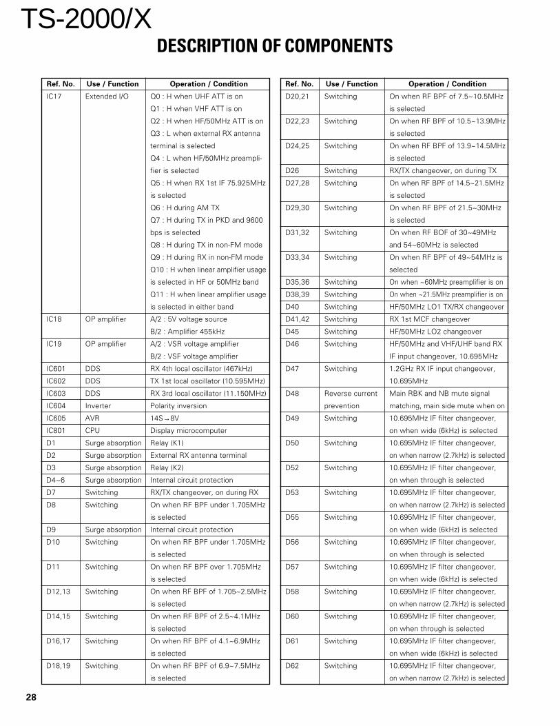
28
TS-2000/X
Ref. No. Use / Function Operation / Condition
IC17 Extended I/O Q0 : H when UHF ATT is on
Q1 : H when VHF ATT is on
Q2 : H when HF/50MHz ATT is on
Q3 : L when external RX antenna
terminal is selected
Q4 : L when HF/50MHz preampli-
fier is selected
Q5 : H when RX 1st IF 75.925MHz
is selected
Q6 : H during AM TX
Q7 : H during TX in PKD and 9600
bps is selected
Q8 : H during TX in non-FM mode
Q9 : H during RX in non-FM mode
Q10 : H when linear amplifier usage
is selected in HF or 50MHz band
Q11 : H when linear amplifier usage
is selected in either band
IC18 OP amplifier A/2 : 5V voltage source
B/2 : Amplifier 455kHz
IC19 OP amplifier A/2 : VSR voltage amplifier
B/2 : VSF voltage amplifier
IC601 DDS RX 4th local oscillator (467kHz)
IC602 DDS TX 1st local oscillator (10.595MHz)
IC603 DDS RX 3rd local oscillator (11.150MHz)
IC604 Inverter Polarity inversion
IC605 AVR 14S→8V
IC801 CPU Display microcomputer
D1 Surge absorption Relay (K1)
D2 Surge absorption External RX antenna terminal
D3 Surge absorption Relay (K2)
D4~6 Surge absorption Internal circuit protection
D7 Switching RX/TX changeover, on during RX
D8 Switching On when RF BPF under 1.705MHz
is selected
D9 Surge absorption Internal circuit protection
D10 Switching On when RF BPF under 1.705MHz
is selected
D11 Switching On when RF BPF over 1.705MHz
is selected
D12,13 Switching On when RF BPF of 1.705~2.5MHz
is selected
D14,15 Switching On when RF BPF of 2.5~4.1MHz
is selected
D16,17 Switching On when RF BPF of 4.1~6.9MHz
is selected
D18,19 Switching On when RF BPF of 6.9~7.5MHz
is selected
Ref. No. Use / Function Operation / Condition
D20,21 Switching On when RF BPF of 7.5~10.5MHz
is selected
D22,23 Switching On when RF BPF of 10.5~13.9MHz
is selected
D24,25 Switching On when RF BPF of 13.9~14.5MHz
is selected
D26 Switching RX/TX changeover, on during TX
D27,28 Switching On when RF BPF of 14.5~21.5MHz
is selected
D29,30 Switching On when RF BPF of 21.5~30MHz
is selected
D31,32 Switching On when RF BOF of 30~49MHz
and 54~60MHz is selected
D33,34 Switching On when RF BPF of 49~54MHz is
selected
D35,36 Switching On when ~60MHz preamplifier is on
D38,39 Switching On when ~21.5MHz preamplifier is on
D40 Switching HF/50MHz LO1 TX/RX changeover
D41,42 Switching RX 1st MCF changeover
D45 Switching HF/50MHz LO2 changeover
D46 Switching HF/50MHz and VHF/UHF band RX
IF input changeover, 10.695MHz
D47 Switching 1.2GHz RX IF input changeover,
10.695MHz
D48 Reverse current Main RBK and NB mute signal
prevention matching, main side mute when on
D49 Switching 10.695MHz IF filter changeover,
on when wide (6kHz) is selected
D50 Switching 10.695MHz IF filter changeover,
on when narrow (2.7kHz) is selected
D52 Switching 10.695MHz IF filter changeover,
on when through is selected
D53 Switching 10.695MHz IF filter changeover,
on when narrow (2.7kHz) is selected
D55 Switching 10.695MHz IF filter changeover,
on when wide (6kHz) is selected
D56 Switching 10.695MHz IF filter changeover,
on when through is selected
D57 Switching 10.695MHz IF filter changeover,
on when wide (6kHz) is selected
D58 Switching 10.695MHz IF filter changeover,
on when narrow (2.7kHz) is selected
D60 Switching 10.695MHz IF filter changeover,
on when through is selected
D61 Switching 10.695MHz IF filter changeover,
on when wide (6kHz) is selected
D62 Switching 10.695MHz IF filter changeover,
on when narrow (2.7kHz) is selected
DESCRIPTION OF COMPONENTS

29
TS-2000/X
Ref. No. Use / Function Operation / Condition
D64 Switching 10.695MHz IF filter changeover,
on when through is selected
D65 Reverse current Matching of main VHF and main
prevention UHF changeover signal
D66 Detection NB switching pulse detection
D67 Switching 455kHz IF filter changeover
D68 Switching On when FM mode is selected in
main band
D69 Switching 455kHz IF filter changeover
D70,71 Switching 455kHz IF filter changeover
D73 Switching On when non-FM mode is select-
ed in main band
D75 Switching On during HF/50MHz TX
D76~79 Variable capacitor Voltage varies (2 stages) according
to the TX band
D80 Switching TX IF output HF/50MHz, VHF/UHF
changeover
D81 Switching TX IF output 1.2GHz changeover
D82 PIN diode TX IF gain variable according to TX power
D83 Reverse current Matching of VTXB and UTXB
prevention
D84 PIN diode TX gain setting of each band
D85 Reverse current
prevention
D86 LED For constant voltage
D87~89 Reverse current
prevention
D90 Switching TX IF FM mode/non-FM mode
changeover, 10.595MHz
D91 Variable capacitor FM modulation 10.595MHz
D92,93 Reverse current Creates IF TXB
prevention
D94,95 Reverse current Creates IF RXB
prevention
D96 Zener diode Stabilizes minus power source to –6V
D97 Rectifier Creates minus voltage
D98 Surge absorption Relay (K3)
D99 Reverse current Matching of start signals from PC
prevention and mobile panel
D100 Zener diode Port protection
D101 Poly-switch Over voltage detection
D102 Zener diode Reference voltage of constant voltage
power source for mobile panel
D103,104 Surge absorption
D105 LED Creates reference voltage
D106 Reverse current External ALC matching
prevention
D107 Zener diode External ALC voltage shift
Ref. No. Use / Function Operation / Condition
D108 Zener diode Voltage shift
D109,110 Reverse current External ALC matching
prevention
D111 Reverse current
prevention
D112 Zener diode Port protection
D113 Zener diode Voltage shift, lower power when
power voltage drops
D114 Zener diode Set so the power does not to rise
when the power voltage goes up
D115,116 Reverse current Meter line
prevention
D117,118 Reverse current External standby
prevention
D119 Reverse current UHF forward wave
prevention
D120 Reverse current UHF reflected wave
prevention
D121 Reverse current 1.2GHz forward wave
prevention
D122 Reverse current 1.2GHz reflected wave
prevention
D123 Reverse current VHF forward wave
prevention
D124 Reverse current VHF reflected wave
prevention
D130 PIN diode RX gain adjustment 455kHz
D700~702 Reverse current
prevention
D703 Variable capacitor Voltage varies (2 stages) according
to the TX band
D704,705 Switching On when preamplifier is on at
21.5~60MHz
D706 Reverse current On at 21.5~60MHz
prevention
D707 Rectifier Noise rectification for FM squelch
D708 Reverse current Leak current prevention
prevention
D709 Zener diode 8V→5V
D710 Voltage shift Temperature compensation
D711 Reverse current Discharge path (non-FM mode)
prevention
D712,713 Cliper External modulation input
D714 Voltage shift
D715 Variable capacitor Voltage varies (2 stages) according
to the TX band
D716 Reverse current
prevention
DESCRIPTION OF COMPONENTS

30
TS-2000/X
Ref. No. Use / Function Operation / Condition
D717 Surge protection
D719,720 Zener diode External surge voltage protection
D721 Reverse current
prevention
D801 LED On in main band TX mode
D802 LED On when main band BSY
D803 LED On in sub band TX mode
D804 LED On when sub band BSY
D805~809 Reverse connection Key matrix
prevention
D810~824 LED Key illumination
D826~834 LED Key illumination
D825 LED On when FUNC switch is selected
D950~952 Reverse current
prevention
D953 LED On when TNC 9600 bps is selected
D954 LED TNC TX buffer state display
D955 LED TNC connection state display
D956 LED On when MULTI is selected
D957 LED Lights when the sub is on
Ref. No. Use / Function Operation / Condition
Q35 Switching Sub RX AM power supply
Q36 Switching VHF sub RX IC6 power supply
Q37 Amplifier Sub RX 1st IF signal amplification
Q38 Amplifier Main RX 1st IF signal AGC control
amplification
Q39 DC amplifier Sub RX AM AGC control signal DC
amplification
Q40,41 Switching Sub RX FM wide/narrow change-
over control
Q42,43 Mixer Main RX 2nd mixer
Q44 Amplifier Main RX 2nd mixer local oscillator
signal amplification
Q45 Amplifier Sub RX AM signal amplification
Q46,47 Mixer TX mixer
Q48 Amplifier Sub RX AM signal amplification
Q50 Amplifier TX mixer local oscillator signal amplification
Q51 Amplifier Sub RX AM signal amplification
Q55 Switching VHF sub RX power supply
Q56 Switching UHF sub RX power supply
Q57 Switching Sub RX IF amplifier gain RBK control
Q58 Switching VHF main RX preamplifier through
Q59 Switching UHF main RX preamplifier through
Q60 Switching VHF/UHF TX wide-band amplifier
power supply
Q61 Amplifier Main RX 2nd IF signal amplification
Q62 Switching VHF/UHF TX wide-band amplifier
power supply
Q63 Amplifier Sub RX squelch signal noise amplification
Q65 Amplifier 31.2MHz reference signal amplification
Q66,67 Switching Sub RX band changeover control
Q400~402 Active LPF Comparison frequency 5kHz
Q403 Switching HF LO2 VCO changeover
Q404 Switching Sub VCO1 oscillation frequency
changeover
Q405 Switching Sub VCO2 oscillation frequency
changeover
Q406 SUB VCO1 322.950~426.040MHz (K)
371.475~381.475MHz (E)
Q407 SUB VCO2 354.950~465.050MHz (K)
405.050~409.050MHz (E)
Q409 LO2 VCO 58.390~65.230MHz
Q410 Switching Sub VCO1 changeover
Q411 Switching Sub VCO2 changeover
Q412 Doubler 15.6MHz x 2 = 31.2MHz
Q413 Amplifier For sub VCO1
(322.950~426.040MHz (K)
371.475~381.475MHz (E))
Q414 Amplifier For sub VCO2
(354.950~465.050MHz (K)
405.050~409.050MHz (E))
TX-RX 2 UNIT (X57-606X-XX)
Ref. No. Use / Function Operation / Condition
Q1 Switching UHF RX ATT control
Q2 Switching VHF RX ATT control
Q3 Switching Sub band local oscillator power supply
Q11 Switching VHF RX power supply
Q13 Switching UHF power supply
Q14 Amplifier UHF preamplifier
Q15 Amplifier VHF preamplifier
Q16 Switching UHF RX power supply
Q17 Amplifier UHF TX signal amplification
Q18 Amplifier VHF TX signal amplification
Q19 Amplifier UHF RX signal amplification
Q20 Amplifier VHF TX signal amplification
Q21 Amplifier UHF main RX signal amplification
Q22,23 Amplifier VHF sub RX signal amplification
Q24 Amplifier VHF main RX signal amplification
Q25 Amplifier VHF sub RX signal amplification
Q26 Amplifier UHF TX signal amplification
Q30 Amplifier Main RX local oscillator signal amplification
Q31 Switching Main RX mixer power supply
Q32 Amplifier VHF sub RX local oscillator signal
amplification
Q33 Amplifier UHF sub RX local oscillator signal
amplification
Q34 Amplifier VHF/UHF TX local oscillator signal
amplification
DESCRIPTION OF COMPONENTS

31
TS-2000/X
Ref. No. Use / Function Operation / Condition
Q415 Buffer amplifier For HF LO2 (58.390~65.230MHz)
Q416 Buffer amplifier PLL input buffer
(322.950~465.050MHz (K)
371.475~409.050MHz (E))
Q417 Amplifier For VHF/UHF LO2 (31.2MHz)
Q418,419 Ripple filter 8V
Q420 Buffer amplifier 15.6MHz
Q421 Amplifier For HF LO2 output (58.390~65.230MHz)
Q423~425 Buffer amplifier DDS input buffer (31.2MHz)
Q426 Switching For Q427
Q427 HF REF VCO 31.130~32.834MHz
Q428 Amplifier For HF REF VCO (31.130~32.834MHz)
Q429 Buffer amplifier For VHF DDS
(9.014~9.322MHz (K)
9.112~9.210MHz (E))
Q430 Buffer amplifier For UHF DDS
(8.328~8.475MHz (K)
8.344~8.469MHz (E))
Q431 UHF VCO 378.105~418.205MHz (K)
388.105~398.205MHz (E)
Q432 Buffer amplifier For HF DDS (7.792~8.209MHz)
Q433 VHF VCO 183.795~193.895MHz (K)
185.795~187.895MHz (E)
Q434 Switching UHF VCO changeover
Q435 Amplifier For UHF VCO
(378.105~418.205MHz (K)
388.105~398.205MHz (E))
Q436 Ripple filter 8V
Q437 Amplifier For VHF VCO
(183.795~193.895MHz (K)
185.795~187.895MHz (E))
Q438 Ripple filter 8V
Q489 Switching VHF REF VCO changeover
Q441 VHF REF VCO 36.058~37.288MHz
Q444 Amplifier For VHF REF VCO (36.058~37.288MHz)
Q446 Ripple filter 8V
Q447 Active LPF Comparison 975~1375kHz
Q448,449 Active LPF Comparison 520~529kHz
Q450 Active LPF Comparison 975~1375kHz
Q451 Active LPF Comparison 520~529kHz
Q452 Active LPF Comparison 975~1375kHz
Q453 Switching HF VCO1 changeover
Q454 switching HF VCO3 changeover
Q455 Ripple filter 8V
Q457 Amplifier For PLL input
(183.795~193.895MHz (K)
185.795~187.895MHz (E))
Q458 Ripple filter 8V
Q459 HFLO1, VCO1 75.855~86.085MHz
Q460 HFLO1, VCO3 112.825~129.085MHz
Ref. No. Use / Function Operation / Condition
Q461 Amplifier For PLL input
(378.105~418.205MHz (K)
388.105~398.205MHz (E))
Q462 Amplifier For HF VCO (75.855~129.085MHz)
Q463 Switching HF VCO2 changeover
Q464 HFLO1, VCO2 92.825~106.085MHz
Q469~472 Switching VHF/UHF LO1 output changeover
Q473 Ripple filter 8V
Q474 Switching VHF/UHF LO1 output changeover
Q476 Amplifier For HF LO1 output
IC2 Serial/parallel Power, AM FM wide/narrow control
signal conversion
IC3 Wide-band amplifier VHF/UHF TX amplifier
IC4 Mixer Main RX 1st mixer
IC5 Mixer Sub RX 1st mixer
IC6 Divider Sub VHF local oscillator 1/2 divider
IC7 FM IC Sub band FM detection
IC8 Multiplexer Sub band FM/AM audio output
changeover
IC9 OP amplifier Sub band FM demodulated signal
amplification
IC400 AVR 10V→8V
IC401 PLL For HF LO2 VCO
IC402 PLL For sub VCO
IC403 AVR 8V→5V
IC404 Serial/parelle VCO changeover signal output
conversion
IC405 Wide-band For sub LO1 output
amplifier (322.950~ 465.050MHz (K)
371.475~405.050MHz (E))
IC406 DDS For VHF REF VCO
(9.014~9.322MHz (K)
9.112~9.210MHz (E))
IC407 DDS For UHF VCO
(8.328~8.476MHz (K)
8.344~8.469MHz (E))
IC408 DDS For HF REF VCO (7.792~8.209MHz)
IC409 PLL For HF REF VCO
IC410 PLL For VHF VCO
IC411 PLL For VHF REF VCO
IC412 PLL For UHF VCO
IC414 PLL For HF VCO
IC415 Wide-band For VHF/UHF RX LO1 output
amplifier (183.895~418.105MHz (K)
185.895~398.105MHz (E))
IC416 Wide-band For VHF/UHF TX LO1 output
amplifier (183.795~418.205MHz (K)
185.795~398.205MHz (E))
D6 Switching On in UHF TX mode
D7 Switching On in VHF TX mode
DESCRIPTION OF COMPONENTS
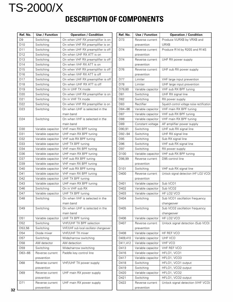
32
TS-2000/X
Ref. No. Use / Function Operation / Condition
D9 Switching On when UHF RX preamplifier is on
D10 Switching On when VHF RX preamplifier is on
D11 Switching On when UHF RX preamplifier is off
D12 Switching On when UHF RX ATT is on
D13 Switching On when VHF RX preamplifier is off
D14 Switching On when VHF RX ATT is on
D15 Switching On when VHF RX preamplifier is off
D16 Switching On when VHF RX ATT is off
D17 Switching On when UHF RX preamplifier is off
D18 Switching On when UHF RX ATT is off
D19 Switching On in UHF TX mode
D20 Switching On when UHF RX preamplifier is on
D21 Switching On in VHF TX mode
D22 Switching On when VHF RX preamplifier is on
D23 Switching On when UHF is selected in the
main band
D24 Switching On when VHF is selected in the
main band
D30 Variable capacitor VHF main RX BPF tuning
D31 Variable capacitor UHF main RX BPF tuning
D32 Variable capacitor VHF sub RX BPF tuning
D33 Variable capacitor UHF TX BPF tuning
D34 Variable capacitor VHF main RX BPF tuning
D36 Variable capacitor UHF main RX BPF tuning
D37 Variable capacitor VHF sub RX BPF tuning
D39 Variable capacitor VHF main RX BPF tuning
D40 Variable capacitor VHF sub RX BPF tuning
D41 Variable capacitor VHF main RX BPF tuning
D42 Variable capacitor UHF TX BPF tuning
D43 Variable capacitor UHF main RX BPF tuning
D46 Switching On in VHF sub RX
D47 Variable capacitor UHF TX BPF tuning
D48 Switching On when VHF is selected in the
main band
D49 Switching On when UHF is selected in the
main band
D51 Variable capacitor UHF TX BPF tuning
D52 Switching VHF/UHF TX BPF selection
D53,56 Switching VHF/UHF sub local oscillator changeover
D54 Diode mixer VHF/UHF TX mixer
D57 Switching Wide/narrow switching
D58 AM detector AM detection
D59 Switching Wide/narrow switching
D63~66 Reverse current Paddle key control line
prevention
D68 Reverse current VHF/UHF TX power supply
prevention
D69 Reverse current UHF main RX power supply
prevention
D71 Reverse current UHF main RX power supply
prevention
Ref. No. Use / Function Operation / Condition
D73 Reverse current Produce VURXB by VRXB and
prevention URXB
D74 Reverse current Produce R14 by R20S and R14S
prevention
D74 Reverse current UHF RX power supply
prevention
D76 Reverse current UHF sub RX power supply
prevention
D77 Limiter VHF large input prevention
D78 Limiter UHF large input prevention
D79,80 Variable capacitor VHF sub RX BPF tuning
D81 Switching UHF RX signal line
D82 Switching RX power supply
D83 Rectifier Squelch control voltage noise rectification
D84~86 Variable capacitor VHF main RX BPF tuning
D87 Variable capacitor VHF sub RX BPF tuning
D88 Variable capacitor VHF main RX BPF tuning
D89 Constant voltage AF amplifier power supply
D90,91 Switching UHF sub RX signal line
D92~94 Switching UHF RX signal line
D95 Switching Sub RX signal line
D96 Switching VHF sub RX signal line
D97 Switching RX power supply
D100 Variable capacitor VHF sub RX BPF tuning
D98,99 Reverse current D95 control line
prevention
D101 Switching VHF sub RX signal line
D400 Reverse current Unlock signal detection (HF LO2 VCO)
prevention
D401 Variable capacitor Sub VCO1
D402 Variable capacitor Sub VCO2
D403 Variable capacitor HF LO2 VCO
D404 Switching Sub VCO1 oscillation frequency
changeover
D405 Switching Sub VCO2 oscillation frequency
changeover
D406 Variable capacitor HF LO2 VCO
D407 Reverse current Unlock signal detection (Sub VCO)
prevention
D408 Variable capacitor HF REF VCO
D409,410 Variable capacitor UHF VCO
D411,412 Variable capacitor VHF VCO
D413 Variable capacitor VHF REF VCO
D416 Variable capacitor HFLO1, VCO1
D417 Variable capacitor HFLO1, VCO3
D418 Switching HFLO1, VCO1 output
D419 Switching HFLO1, VCO2 output
D420 Variable capacitor HFLO1, VCO2
D421 Switching HFLO1, VCO2 output
D422 Reverse current Unlock signal detection (VHF VCO)
prevention
DESCRIPTION OF COMPONENTS

33
TS-2000/X
Ref. No. Use / Function Operation / Condition
D423 Reverse current Unlock signal detection (UHF VCO)
prevention
D426 Switching On in main VHF RX mode
D427 Switching On in VHF TX mode
D428 Switching On in main UHF RX mode
D429 Switching On in UHF TX mode
D430 Switching On in main VHF RX mode
D431 Switching On VHF TX mode
D432 Switching On in main UHF RX mode
D433 Switching On in UHF TX mode
D434,441 Switching On in main VHF RX mode
D435,442 Switching On in main UHF RX mode
D436,443 Switching On in VHF TX mode
D437,444 Switching On in UHF TX mode
D438 Reverse current Unlock signal detection (HF VCO)
prevention
D439,440 Switching Filter changeover, on when 0.03~
16.99MHz
D445~447 Reverse current HF LO2 is selected when HF band mode
prevention
Ref. No. Use / Function Operation / Condition
Q20 High-frequency Amplifies 1104~1165MHz local
amplifier oscillation signal
Q301 VCO FET for oscillation
Q302 High-frequency VCO oscillation buffer amplifier
amplifier
Q303 RX IF amplifier Amplifies the 10.695MHz IF signal
Q304 TX IF amplifier Amplifies the 10.595MHz IF signal
Q305~307 LPF PLL loop LPF
Q310,311 Amplifier Amplifies 31.2MHz signal
Q312 PLL reference Amplifies PLL reference signal
signal amplifier
Q313,314 Mixer for PLL Input : 31.2MHz, 8.323~8.488MHz
reference signal Output : 39.523~39.688MHz
Q315 Switch RX signal mute
IC1 TX RF amplifier
IC2 Drive power module Amplifies to approximately 1W
IC3 Final power module Amplifies to approximately 10W
IC4 DDS Produces an approximately 8.4MHz
signal from the 31.2MHz reference signal
IC5 PLL VCO input : 552.253~582.303MHz
Reference input : 39.523~39.688MHz
D1 TX mixer Converts 135.395MHz signal to
1240~1300MHz
D2 Q5 base voltage A voltage more than that stipulated
stabilization for Q5 base is not to be applied
D3 Forward wave
detection
D4 Reflected wave
detection
D5~7 TX/RX changeover On when TX
D8 Local signal Supplies a 124.8MHz signal to Q1 and
changeover Q2 during TX and to Q7 and Q8 during RX
D9 AGC starting control Speeds the AGC start
D10 Local signal Goes ON during TX and supplies a
changeover 1104~1165MHz signal to D1
D11 Local signal Goes ON during RX and supplies a
changeover 1104~1165 MHz signal to Q10
D12 Power supply Supply the power to the local oscillator
unit from 12RXB and 12TXB
D301 VCO Variable capacitance diode for VCO
oscillation
D302 Zener diode A voltage more than that stipulated
for Q12 is not to be applied
D303 TX/RX changeover On when TX
D304 Switch PLL unlock detection
D305 VCO Variable capacitance diode for VCO
oscillation
DESCRIPTION OF COMPONENTS
TX-RX 3 UNIT (X57-6070-00)
Ref. No. Use / Function Operation / Condition
Q1,2 TX mixer Input : 10.595MHz, 124.8MHz
Output : 135.395MHz
Q3 TX IF amplifier Amplifies 135.395MHz TX IF
signal
Q4 Power switch Supplies 5V to IC1 during TX
Q5 TX RF amplifier Amplifies 1240~1300MHz TX RF
signal
Q7,8 RX mixer Input : 135.495MHz, 124.8MHz
Output : 10.695MHz
Q9 RX AGC amplifier
Q10 RX mixer Input : 1104~1165MHz, 1240~1300MHz
Output : 135.495MHz
Q11,12 RX RF amplifier Amplifies 1240~1300MHz RX RF signal
Q13 Reference signal Amplifies IC4 reference signal
amplifier (31.2MHz)
Q14 Quadruple Input : 31.2MHz
Output : 124.8MHz
Q15 local oscillation Amplifies local oscillation signal
signal amplifier (124.8MHz)
Q16 Amplifier Amplifies 8.323~8.488MHz signal
Q17 Power filter Smooths power for VCO and loop filter
Q19 Double Output : 1104~1165MHz

34
TS-2000/X
Main CPU : 64F2633xxxx (Control unit IC8)
Pin function
No. Name I/O Function
1 MD1 I Operation mode setting pin 1.
Connect to Vcc.
2 MD2 I Operation mode setting pin 2.
Connect to Vcc.
3,4 NC –
5~8 HA0~HA3 O Address bus.
9 Vss – GND.
10 HA4 O Address bus.
11 Vcc I 3.3V.
12~14 HA5~HA7 O Address bus.
15 Vss – GND.
16 ADC1 O Analog switch control signal.
17 PVcc I 5V.
18 ADC2 O Analog switch control signal.
19 PSC O Power relay control.
20 DASH I Electronic key dash signal.
21 DOT I Electronic key dot signal.
22 STSC O RS-232 IC start instruction.
23 CKY O Transmission power output specification.
24 CTS2 I UART operation instruction input from
personal computer control.
25 RTS2 O UART operation instruction output to
personal computer control.
26 TXD2 O Data output to PC/IF.
27 RXD2 I Data input from PC/IF.
28 RES O Peripheral equipment reset input.
29 Vss – GND.
30 BEEP O Beep pattern output to DSP.
31 PCK O PLL unit common clock output.
32 PDA O PLL unit common data output.
33 DATA O Common data output.
34 PSW I Power switch interrupt.
35,36 NC –
37 CLOCK O Common clock output.
38 MRBK O Main RBK output.
39 SRBK O Sub RBK output.
40 MABK O Main ABK output.
41 SABK O Sub ABK output.
No. Name I/O Function
42 DRES O DSP reset output.
43 ULK I Main/sub common unlock signal.
44 12ULK I 1.2GHz band unlock signal.
45 DREN O DRU-3 enable.
46 ESCK O EEPROM clock output.
47 ESI O EEPROM data output.
48 Vss – GND.
49 HD0 O Data bus.
50 PVcc I 5V.
51~57 HD1~HD7 O Data bus.
58 TXD0 O Data output to main unit panel.
59 RXD0 I Data input from main unit panel.
60 PVcc I 5V. Power supply pin for pin 52~61.
61 START I Interrupt for returning from sleep mode.
(PC/mobile head)
62 Vss – GND.
63 TXD1 O Data output to mobile head.
64 RXD1 I Data input from mobile head.
65 BOVR I Over voltage detection interrupt.
66 TTO O AT-300 control signal.
67,68 NC –
69 TSO O AT-300 control signal.
70 TTI I AT-300 control signal.
71 AMD I Amplitude comparison detection inst-
ruction input.
72 CSD2 O DSP control chip select 2
73 CSD1 O DSP control chip select 1.
74 TSI I AT-300 control signal.
75 NC O
76 PLLVcc I Internal PLL oscillator power 3.3V.
77 PLLCAP I
78 PLLVss – Internal PLL oscillator GND.
79 RESET I Hard reset input.
80 NMI I Normally H.
81 STBY I Hardware standby pin. Normally : H
82 FWE I Flash light enable.
Normally : L, During writing : H
83 XTAL I Crystal oscillator 11.0592MHz.
SEMICONDUCTOR DATA

35
TS-2000/X
No. Name I/O Function
84 Vcc I 3.3V.
85 EXTAL I Crystal oscillator 11.0592MHz.
86 Vss – GND.
87,88 NC I
89 PVcc I 3.3V.
90 PHD I Phase comparison detection instruction
input.
91 Vss – GND.
92 NC O
93 HRD O External address space lead pin.
Normally : H
94 HWR O External space write strobe (D15~D8).
95 BACKUP I Voltage reduction interrupt.
96 WAIT I Bus cycle wait state request.
97 FEN2 O Final serial-parallel enable 2 (AT).
98 FEN1 O Final serial-parallel enable 1 (LPF).
99,100 NC –
101 Avcc I 5V.
102 VREF I 5V.
103 MSM I Main SM voltage input.
104 SSM I Sub SM voltage input.
105 AXC I SW (VSF/MALT).
106 AYC I SW (VSR/SALT).
107 AZC I SW (MSQ/SMQ).
SEMICONDUCTOR DATA
No. Name I/O Function
108 BXC I SW (MPU/MDN/ALC/Reserve).
109 BYC I SW (THHF/THU/TH12/TEST).
110 PCHECK I Panel CPU connection check input signal.
111 DTDT I DTMF decoder data input.
112 NAR I VS-3 serial data input permission judgment.
113 EOM I DRU-3 message end judgment.
114 KYS I Key jack connection judgment.
115 CTS0 I UART operation instruction input from
main unit panel.
116 KEY I Key down instruction.
117 PKSA I Packet transmission instruction input.
118 SS I PTT transmission instruction input.
119 AVss – GND.
120 LICS O Input latch control chip select.
121 LOCS O Output latch control chip select.
122 DTSTD I DTMF decoder analysis end signal.
123 EDA I EEPROM data input.
124 EEN O EEPROM enable.
125 RST0 O UART operation instruction output to
main unit panel.
126 RXD3 I Data input from TNC.
127 TXD3 O Data output to TNC.
128 MD0 I Operation mode setting pin 0.
Connect to Vss.

36
TS-2000/X
No. Name I/O Function
47 STX O Sub TX LED control signal.
48 MRX O Main RX LED control signal.
49 MTX O Main TX LED control signal.
50 FUNC O FUNC LED control signal.
51 LINH O LCD segment display off control output.
52 LMO O LCD driver control output.
53 LCK O Common clock output.
54 LDA O Common data output.
55 LCS1 O LDC (segment) driver 1 chip select output.
56 LCS2 O LCD (segment) driver 2 chip select output.
57 LCS3 O LCD (dot) driver chip select output.
58 LCS4 O Serial-parallel IC chip select output.
59 LCS5 O Reserve.
60 Vcc – Vcc.
61 LRES – LCD driver reset control signal.
62 Vss – Vss.
63~65 – – Pull up to Vcc.
66~70 S0~S4 O Key scan output bit 0~4
71 PBKC I Backup processing start signal.
72 KC I Key input C.
73 KB I Key input B.
74 KA I Key input A.
75,76 – – Pull up to Vcc.
77~86 K9~K0 I Key input 9~0.
87 SUBS I Sub on/off changover.
88 MAF I Main AF.
89 MSQL I Main SQL.
90 CWBC I CW BC.
91 MRF I Main RF.
92 SAF I Sub AF.
93 SSQL I Sub SQL.
94 AVss – Vss connection.
95 – – Pull up to Vcc.
96 VREF – ADC reference voltage. Vcc connection.
97 AVcc – ADC circuit power. Vcc connection.
98~100 – – Pull up to Vcc.
SEMICONDUCTOR DATA
Pin function
No. Name I/O Function
1,2 KEY O Key illumination LED control signal.
3 – – Pull up to Vcc.
4 LSUB O Sub LED control signal.
5 MULTI O Multi LED control signal.
6 – – Vss connection.
7 – – Pull down to Vss.
8,9 – – Pull up to Vcc.
10 RES I Reset.
11 XOUT O System clock.
12 Vss – Vss.
13 XIN I System clock.
14 Vcc – Vcc.
15 – – Pull up to Vcc.
16 MUL1 I Multi/CH encoder interrupt port.
17 LOW1 I Low encoder interrupt port.
18 HI1 I High encoder interrupt port.
19 MAA I Main encoder A.
20 MAB I Main encoder B.
21 RITA I RIT encoder A.
22 RITB I RIT encoder B.
23 MUL2 I Multi/CH encoder data input.
24 LOW2 I Low encoder data input.
25 HI2 I High encoder data input.
26~28 – – Pull up to Vcc.
29 CON O CON LED control signal.
30 STA O STA LED control signal.
31 9.6K O 9.6K KED control signal.
32 – – Pull down to Vss.
33 TXD0 O UART data transmission port to main CPU.
34 RXD0 I UART data reception port from main CPU.
35 RTS0 O RTS output to main CPU.
36 CTS0 I RTS input from main CPU.
37~40 – – Pull down to Vss.
41~44 – – Pull up to Vcc.
45 DIM O LED dimmer control signal.
46 SRX O Sub RX LED control signal.
Panel CPU : 30624FGAGxxxxx (TX-RX 1 unit IC801)
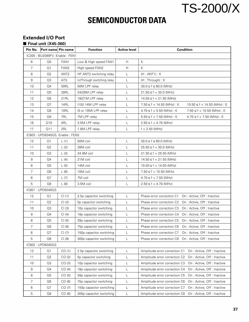
37
TS-2000/X
Extended I/O Port
Final unit (X45-360)
Pin No. Port name Pin name Function Active level Condition
IC205 : BU2099FV, Enable : FEN1
6 Q0 FAN1 Low & High speed FAN1 H K
7 Q1 FAN2 High speed FAN2 H K
8 Q2 ANT2 HF ANT2 switching relay L (H : ANT1) : K
9 Q3 ATS In/Through switching relay L (H : Through) : K
10 Q4 50RL 50M LPF relay L 30.0 ≤ f ≤ 60.0 (MHz)
11 Q5 28RL 24/28M LPF relay L 21.50 ≤ f < 30.0 (MHz)
12 Q6 21RL 18/21M LPF relay L 14.50 ≤ f < 21.50 (MHz)
13 Q7 14RL (10/) 14M LPF relay L 7.50 ≤ f < 14.50 (MHz) : K 10.50 ≤ f < 14.50 (MHz) : E
14 Q8 10RL (5 or 10M) LPF relay L 4.70 ≤ f < 5.50 (MHz) : K 7.50 ≤ f < 10.50 (MHz) : E
15 Q9 7RL 7M LPF relay L 5.50 ≤ f < 7.50 (MHz) : K 4.70 ≤ f < 7.50 (MHz) : E
16 Q10 4RL 3.5M LPF relay L 2.50 ≤ f < 4.70 (MHz)
17 Q11 2RL 1.8M LPF relay L f < 2.50 (MHz)
IC803 : UPD6345GS, Enable : FEN2
12 Q1 L (1) 50M coil L 30.0 ≤ f ≤ 60.0 (MHz)
11 Q2 L (2) 28M coil L 25.50 ≤ f < 30.0 (MHz)
10 Q3 L (3) 24.9M coil L 21.50 ≤ f < 25.50 (MHz)
9 Q4 L (4) 21M coil L 14.50 ≤ f < 21.50 (MHz)
8 Q5 L (5) 14M coil L 10.50 ≤ f < 14.50 (MHz)
7 Q6 L (6) 10M coil L 7.50 ≤ f < 10.50 (MHz)
6 Q7 L (7) 7M coil L 4.70 ≤ f < 7.50 (MHz)
5 Q8 L (8) 3.5M coil L 2.50 ≤ f < 4.70 (MHz)
IC801 : UPD6345GS
12 Q1 CI (1) 2.5p capacitor switching L Phase error correction C1 On : Active, Off : Inactive
11 Q2 CI (2) 5p capacitor switching L Phase error correction C2 On : Active, Off : Inactive
10 Q3 CI (3) 10p capacitor switching L Phase error correction C3 On : Active, Off : Inactive
9 Q4 CI (4) 18p capacitor switching L Phase error correction C4 On : Active, Off : Inactive
8 Q5 CI (5) 39p capacitor switching L Phase error correction C5 On : Active, Off : Inactive
7 Q6 CI (6) 75p capacitor switching L Phase error correction C6 On : Active, Off : Inactive
6 Q7 CI (7) 150p capacitor switching L Phase error correction C7 On : Active, Off : Inactive
5 Q8 CI (8) 300p capacitor switching L Phase error correction C8 On : Active, Off : Inactive
IC802 : UPD6345GS
12 Q1 CO (1) 2.5p capacitor switching L Amplitude error correction C1 On : Active, Off : Inactive
11 Q2 CO (2) 5p capacitor switching L Amplitude error correction C2 On : Active, Off : Inactive
10 Q3 CO (3) 10p capacitor switching L Amplitude error correction C3 On : Active, Off : Inactive
9 Q4 CO (4) 18p capacitor switching L Amplitude error correction C4 On : Active, Off : Inactive
8 Q5 CO (5) 39p capacitor switching L Amplitude error correction C5 On : Active, Off : Inactive
7 Q6 CO (6) 75p capacitor switching L Amplitude error correction C6 On : Active, Off : Inactive
6 Q7 CO (7) 150p capacitor switching L Amplitude error correction C7 On : Active, Off : Inactive
5 Q8 CO (8) 300p capacitor switching L Amplitude error correction C8 On : Active, Off : Inactive
SEMICONDUCTOR DATA

38
TS-2000/X
Control unit (X53-391)
Pin No. Port name Pin name I/O Function
IC25 : TC74VHC573FT
19 Q0 PENA O PLL serial-parallel enable A
18 Q1 PEN1 O PLL enable 1
17 Q2 PEN2 O PLL enable 2
16 Q3 PEN3 O PLL enable 3
15 Q4 PEN4 O PLL enable 4
14 Q5 PEN5 O PLL enable 5
13 Q6 PEN6 O PLL enable 6
12 Q7 DSPW O DSP control signal
IC24 : TC74VHC573FT
19 Q0 DEN1 O DDS enable 1
18 Q1 DEN2 O DDS enable 2
17 Q2 DEN3 O DDS enable 3
16 Q3 DEN4 O DDS enable 4
15 Q4 DEN5 O DDS enable 5
14 Q5 DEN6 O DDS enable 6
13 Q6 12EN1 O 1.2G enable 1
12 Q7 12EN2 O 1.2G enable 2
IC22 : TC74VHC573FT
19 Q0 IEN1 O IF serial-parallel enable 1
18 Q1 IEN2 O IF serial-parallel enable 2
17 Q2 IEN3 O IF serial-parallel enable 3
16 Q3 IEN4 O IF DAC enable 5
15 Q4 EIN5 O IF DAC enable 6
14 Q5 DTCLK O DTMF clock
13 Q6 REN1 O RF serial-parallel enable 1
12 Q7 VCS O VS-3 chip select
IC21 : TC74VHC573FT
19 Q0 SRXC O DSP control signal
18 Q1 DSPEN1 O DSP control signal
17 Q2 DSPEN2 O DSP CODEC enable
Pin No. Port name Pin name I/O Function
16 Q3 AMU O AF mute signal
15 Q4 12EN3 O 1.2G enable 3
14 Q5 SQC O For TNC
13 Q6 ISTBY O STBY for TNC
12 Q7 RTS3 O For tNC
IC23 : TC74VHC573FT
19 Q0 HFTXC O HF TX power start instruction
18 Q1 HFRXC O HF RX power start instruction
17 Q2 VTXC O VHF TX power start instruction
16 Q3 VRXC O VHF RX power start instruction
15 Q4 UTXC O UHF TX power start instruction
14 Q5 URXC O UHF RX power start instruction
13 Q6 12TXC O 1.2G TX power start instruction
12 Q7 12RXC O 1.2G RX power start instruction
IC20 : TC74VHC573FT
2 D0 SPS I SP2 connection detection
3 D1 PKSI I PKS for TNC
4 D2 S9600 I For TNC
5 D3 PMUTE I Mute instruction from modem IC
6 D4 12OP I 1.2G unit connection detection
7 D5 CTS3 I For TNC
8 D6 STA I STA instruction from modem IC
9 D7 CON I CON instruction from modem IC
IC19 : TC74VHC573FT
2 D0 SIM0 I Type setting 0
3 D1 SIM1 I Type setting 1
4 D2 SIM2 I Type setting 2
5 D3 SIM3 I Type setting 3
6 D4 SIM4 I Type setting 4
7 D5 SIM5 I Type setting 5
8 D6 SIM6 I Type setting 6
9 D7 SIM7 I Type setting 7
IC530 : BU2099FV, Enable : DSPEN2
Pin No. Port name Pin name Function Active level Condition
6 Q0 MIC TX input (Microphone selection) H TX from microphone
7 Q1 ACC12 TX input (ACC 1200 bps) H TX 1200 bps from ACC (PKD)
8 Q2 TNC12 TX input (TNC 1200 bps) H TX 1200 bps from built-in TNC
9 Q3 DRU TX input (DRU selection) H TX from DRU
10 Q4 RX12 RX ACC outut (1200 bps) H ACC uses menu 1200 bps
11 Q5 M.REM Remote input (Main) H External trasceiver remote function (Reserved)
12 Q6 S.REM Remote input (Sub) H When the external transceiver remote function is on
13 Q7 M.TNC RX TNC selection (Main) H TNC band (Main)
14 Q8 S.TNC RX TNC selection (Sub) H TNC band (Sub)
15 Q9 MIC.REM Remote input (Microphone) H When the microphone remote function is on
16 Q10 TNC96 TX input (TNC 9600 bps) H 9600 bps TX data from built-in TNC.
17 Q11 NOT96 TX data speed (Other than 9600 bps) H Other than 9600 bps is selected to transmit
SEMICONDUCTOR DATA

39
TS-2000/X
TX-RX 1 unit (X57-605)
Pin No. Port name Pin name Function Active level Condition
IC5 : BU2099FV, Enable : IEN1
6 Q0 BPF12 BPF selection L 49.0MHz ≤ f < 54.0MHz
7 Q1 BPF11 BPF selection L 30MHz ≤ f < 49MHz, 54MHz ≤ f ≤ 60MHz
8 Q2 BPF10 BPF selection L 21.5MHz ≤ f < 30.0MHz
9 Q3 BPF9 BPF selection L 14.5MHz ≤ f < 21.5MHz
10 Q4 BPF8 BPF selection L 13.9MHz ≤ f < 14.5MHz
11 Q5 BPF7 BPF selection L 10.5MHz ≤ f < 13.9MHz
12 Q6 BPF6 BPF selection L 7.50MHz ≤ f < 10.5MHz
13 Q7 BPF5 BPF selection L 6.90MHz ≤ f < 7.50MHz
14 Q8 BPF4 BPF selection L 4.10MHz ≤ f < 6.90MHz
15 Q9 BPF3 BPF selection L 2.50MHz ≤ f < 4.10MHz
16 Q10 BPF2 BPF selection L 1.705MHz ≤ f < 2.50MHz
17 Q11 BPF1 BPF selection L f ≤ 1.705MHz
IC16 : BU2099FV, Enable : IEN2
6 Q0 FIL1 10.695M filter 12k L 10.695M filter 12k
7 Q1 FIL2 10.695M filter 2.7k L 10.695M filter 2.7k
8 Q2 FIL3 10.695M filter through L 10.695M filter through
9 Q3 TCS AT tune switch L Auto tune
10 Q4 455FIL1 455k filter 15k L 455k filter 15k
11 Q5 455FIL2 455k filter 9k L 455k filter 9k
12 Q6 455FIL3 455k filter 2.7k L 455k filter 2.7k
13 Q7 HFRGC HF RX gain adjustment H 21.5MHz ≤ f < 30.0MHz & Pre-amplifier : On
14 Q8 50RGC 50M RX gain adjustment H 30.0MHz ≤ f ≤ 60MHz & Pre-amplifier : On
15 Q9 NC
16 Q10 MSQS Main SQL H/L BUSY : H, Not BUSY : L
17 Q11 SSQS Sub SQL H/L BUSY : H, Not BUSY : L
IC17 : BU2099FV, Enable : IEN3
6 Q0 UATT UHF ATT switch H UHF & ATT on
7 Q1 VATT VHF ATT switch H VHF & ATT on
8 Q2 ATT HF ATT switch H HF & ATT on, or V/U/1.2G
9 Q3 RXANT RX ANT switch L f ≤ 30.0MHz & EXT. RX. ANT. on
10 Q4 PREAMP Pre-amplifier on/off H HF & Pre-amplifier on
11 Q5 MCFSW MCF switch H/L 75M : H, 69M : L
12 Q6 AMC AM switch H 50ms after AM TX is initiated
13 Q7 PKDSW PKD TX switch H When 9600 bps data is transmitted from ACC (PKD)
14 Q8 NFMT* Not FM TX H When the transmission mode is other than FM
15 Q9 NFMR* Not FM RX H When the reception mode is other than FM
16 Q10 RLSW TX-B output switch H f ≤ 30.0MHz or 50MHz Linear ON
17 Q11 LINEAR Linear switch H Linear ON
NFMT*
TX RX
FM L L
AM, CW H L
SSB, FSK H L
NFMR*
TX RX
FM L L
AM, CW L H
SSB, FSK L H
SEMICONDUCTOR DATA

40
TS-2000/X
TX-RX 2 unit (X57-606)
Pin No. Port name Pin name Function Active level Condition
IC2 : BU2099FV
6 Q0 AMSW AM power switch L When the sub AM is selected for receiving
7 Q1 W/NSW Wide/Narrow selection switch L When the sub FM narrow is selected for receiving
8 Q2 R43S Front end selection switch for sub UHF L When the sub UHF is selected for receiving
9 Q3 R14S SUB VHF power switch L When the sub VHF is selected for receiving
10 Q4 8RS1 SLO1 amplifier switch L When the sub VHF is selected for receiving
11 Q5 8RS1/2 SLO1 prescaler (1/2) switch L When the sub UHF is selected for receiving
12 Q6 UPRE UHF pre-amplifier switch L When the UHF receiver and pre-amplifier is off
13 Q7 VPRE VHF pre-amplifier switch L When the VHF receiver and pre-amplifier is off
14 Q8 IMS VHF pre-amplifier through switch L
15 Q9 R50S Front end selection switch for sub UHF L When the sub UHF is selected for receiving
16 Q10 NC
17 Q11 R20S Front end selection switch for sub VHF L When the sub VHF is selected for receiving
IC404 : BU4094BCFV
4 Q1 HF VCO1 VCO1 selection for HF band H When the frequency range of
0.03~17.0MHz is selected
5 Q2 HF VCO2 VCO2 selection for HF band H When the frequency range of
17.0~37.0MHz is selected
6 Q3 HF VCO3 VCO3 selection for HF band H When the frequency range of
37.0~60.0MHz is selected
7 Q4 USW VCO selection for VHF band H When the main band VHF is selected
14 Q5 VSW VCO selection for UHF band H When the main band UHF is selected
13 Q6 BSW2 VCO selection for sub VHF band H When the sub band RX VHF is selected
12 Q7 BSW1 VCO selection for sub UHF band H When the sub band RX UHF is selected
11 Q8 VPRE VCO oscillator range selection for sub band H/L When the sub band is selected for receiving
SEMICONDUCTOR DATA
Conversion Between 5V and 3V :
TC74LVX4245FS (Control unit IC9~11)
Block diagram
G33EN1 (BA)3EN2 (AB)
12
OEDIR
A1
A2
A3
A4
A5
A6
A7
A8
B1
B2
B3
B4
B5
B6
B7
B8
(22)
(21)
(20)
(19)
(18)
(17)
(16)
(15)
(14)
(2)
(3)
(4)
(5)
(6)
(7)
(8)
(9)
(10)
LogicLevel
Converter
Same as above block
DIR
OE
A1
A8
B1
B8
VCCA VCCB
Logic symbol

41
TS-2000/X
Serial-Parallel : BU2099FV
(Final unit IC205, Control unit IC530,
Display unit IC4, TX-RX 1 unit IC5,16,17,
TX-RX 2 unit IC2)
Block diagram
LPF
1
2
3
4
5
6
7
8
9
10 11
12
13
14
15
16
17
18
19
20 VDD
Controlcircuit
OE
SO
Q11
Q10
Q9
Q8
Q7
Q6
Q5Q4
Q3
Q2
Q1
Q0
LCK
CLOCK
DATA
NC
VSS
Ou
tpu
t b
uff
er (
Op
en d
rain
)
12 b
it s
tora
ge
reg
iste
r
12 b
it s
hif
t re
gis
ter
D flip-flop : TC7WH74FU (Filter unit IC2)
Logic diagram
Q
S
C
D
R
Q
(5)
(3)
PR
CK
D
CLR
(7)
(1)
(2)
(6)
Truth table
Input Output Function
CLR PR D CK Q Q
L H X X L H Clear
H L X X H L Preset
L L X X H H –
H H L ↑ L H –
H H H ↑ H L –
H H X ↓ Qn Qn No change
X : Don‘t care
Pin description
No. Name I/O Description
1 Vss – GND
2 NC – NC
3 DATA I Serial data input.
4 CLOCK I Shift register shift clock
(rising edge trigger).
5 LCK I Storage register latch clock
(rising edge trigger).
6~17 Q0~Q11 O Paralle data output
(Qx) (Nch open drain FET).
18 SO O Serial data output.
19 OE I Output enable control input.
20 VDD – Power
Latch data L H
Output FET On Off
Analog Switch : TC74HC4052AFT (Control unit IC6)
Analog Switch : TC74HC4053AFT (Control unit IC5)
Mixer : TC74HC4053AFT (TX-RX 1 unit IC3)
Logic diagram
TC74HC4052AFT TC74HC4053AFT
01G4
AB
INH
X-COM
Y-COM
0X
1X
2X
3X
0Y
1Y
2Y
3Y
(10)
(12)
(14)
(15)
(11)
(1)
(5)
(2)
(4)
(9)(6)
(13)
(3)
MUXDMUX
0...3
0
1
2
3
4 x 30
G2
A
INH
Z-COM
X-COM
0X
0Y
1Y
0Z
1Z
(11) (12)
(2)
(1)
(5)
(3)
(6)
(4)
(14)
MUXDMUX
2 x 02 x 1
0,1
0
1 1X(13)
B(10)
Y-COM(15)
C(9)
Truth table
Control inputs “ON” channel
Inhibit C* B A HC4052A HC4053A
L L L L 0X, 0Y 0X, 0Y, 0Z
L L L H 1X, 1Y 1X, 0Y, 0Z
L L H L 2X, 2Y 0X, 1Y, 0Z
L L H H 3X, 3Y 1X, 1Y, 0Z
L H L L – – 0X, 0Y, 1Z
L H L H – – 1X, 0Y, 1Z
L H H L – – 0X, 1Y, 1Z
L H H H – – 1X, 1Y, 1Z
H X X X None None
X : Don‘t care, * : Except HC4052A
SEMICONDUCTOR DATA
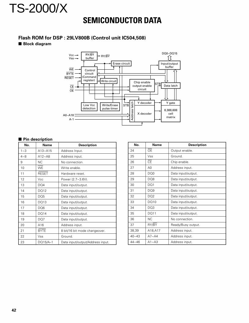
42
TS-2000/X
Flash ROM for DSP : 29LV800B (Control unit IC504,508)
Block diagram
RY/BYbuffer
Controlcircuit
(Commandregister)
Y decoder
X decoder
Y gate
8,388,608cell
matrix
STBLow Vccdetection
STBData latch
DQ0~DQ15RY/BY
Erase circuit
Write circuit
VccVss
WEBYTE
RESET
CEOE
A0~A18A-1
Write/Erasepulse timer
Ad
dre
ss la
tch
Chip enableoutput enable
circuit
Input/outputbuffer
No. Name Description
24 OE Output enable.
25 Vss Ground.
26 CE Chip enable.
27 A0 Address input.
28 DQ0 Data input/output.
29 DQ8 Data input/output.
30 DQ1 Data input/output.
31 DQ9 Data input/output.
32 DQ2 Data input/output.
33 DQ10 Data input/output.
34 DQ3 Data input/output.
35 DQ11 Data input/output.
36 NC No connection.
37 RY/BY Ready/Busy output.
38,39 A18,A17 Address input.
40~43 A7~A4 Address input.
44~46 A1~A3 Address input.
Pin description
No. Name Description
1~3 A13~A15 Address Input.
4~8 A12~A8 Address input.
9 NC No connection.
10 WE Write enable.
11 RESET Hardware reset.
12 Vcc Power (2.7~3.6V).
13 DQ4 Data input/output.
14 DQ12 Data input/output.
15 DQ5 Data input/output.
16 DQ13 Data input/output.
17 DQ6 Data input/output.
18 DQ14 Data input/output.
19 DQ7 Data input/output.
20 A16 Address input.
21 BYTE 8 bit/16 bit mode changeover.
22 Vss Ground.
23 DQ15/A–1 Data input/output/Address input.
SEMICONDUCTOR DATA

43
TS-2000/X
DSP : 320VC5402PGE (Control unit IC515,516)
Pin description
Pin name Type* Description
Data signal
A19~A0 O/Z Parallel address bus A19 (MSB) to A0 (LSB). The low-order 16 bits (A0 to A15) of the address pin are multiplexed to
address to external memory (data, program) or I/O. The high-order 4 bits (A16 to A19) are used to address to external
program space. These pins are high impedance when in hold mode or when OFF is low.
D15~D0 I/O/Z Parallel data bus D15 (MSB) to D0 (LSB). D15 to D0 are multiplexed to transfer data between the core CPU and
external data/program memory or I/O device. The data bus becomes high impedance when data is not output or
RS or HOLD is low. It also becomes high impedance when OFF is low.
The data bus has a bus holder to reduce power consumption of unused pins. When there is a bus holder, external
bias resistors for unused pins are not necessary. When '5402 does not drive the data bus, the bus holder retains the
preceding logic level pin. The '5402 data bus holder is disabled on reset, and enabled/disabled through the BH bit of
the bank switching control register (BSCR).
Initialization, interrupt and reset operation
IACK O/Z Interrupt signal. Interrupt reception and interrupt vector specified by A15 to A0 are fetched by the program counter.
It becomes high impedance when OFF is low.
INT0~ I External user interrupt input. INT0 to INT3 have priorities and can be masked by interrupt mask resister (IMR) and
INT3 interrupt mode bit. Polling and reset can be performed by the interrupt flag register (IFR).
NMI I Interrupt signal that cannot be masked. This external interrupt cannot be masked by INTM or IMR.
When NMI is low, the vector is trapped.
RS I Reset. RS stops DSP operation and initializes the CPU and peripheral. When RS goes high, execution starts from
0FF80h address of the program memory. RS affects various registers and status bits.
MP/MC I Microprocessor/microcomputer mode selection. If it is low on reset, the microcomputer mode is selected, and the
internal program ROM is mapped to the high-order 4K words of the program memory space. If it is high on reset, the
microprocessor mode is selected and the onchip ROM is erased from the program space. This pin is sampled only on
reset, and when the MP/MC bit of the processor mode status (PMST) register is reset, the selected mode is made invalid.
Multi-processing signal
BIO I Branch control. When BIO is active, a conditional branch can be executed. When it is low, the processor executes a
conditional branch. The XC instruction samples BIO condition in the pipeline decode phase. Other instructions sample
BIO in the read phase.
XF O/Z External flag output (latch signal that can be changed by software). It is set to high by SSBX XF instruction, and set to
low by loading an RSBX XF instruction or ST1. This signal is used as a communication or general output signal when
several DSPs are used. It becomes high impedance when OFF signal is at low level, and is set to high level on reset.
Memory control signal
DS O/Z Data, program, or I/O space select signal. It is always at high level, except when it is driven at low level to access a
PS specific external memory space. It is active while the address is effective. In hold mode, it becomes high impedance
IS when the OFF signal is at low level.
MSTRB O/Z Memory strobe signal. It is always at high level, except when accessing data or program memory through an external
bus. In hold mode, it becomes high impedance when the OFF signal is at low level.
READY I Data ready signal. It indicates that an external device has finished preparing accessing a bus.
If it is not ready (READY is at low level), it waits one cycle and checks the READY signal again. At least two software
wait states must be programmed for the processor to detect a READY signal. The READY signal is not sampled until
software wait states are complete.
R/W O/Z Read/write signal. It indicates the direction of data transfer with an external device. It is normally at high level (read
mode) except when it goes low to execute a write operation. In hold mode, it becomes high impedance when the
OFF signal is at low level.
SEMICONDUCTOR DATA

44
TS-2000/X
Pin name Type* Description
IOSTRB O/Z I/O strobe signal. It is always at high level (read mode) except when accessing an I/O device through an external bus.
In hold mode, it becomes high impedance when the OFF signal is at low level.
HOLD I Hold input signal. Address, data, or control signal control input signal. When this signal is accepted, the address,
data, or control signal becomes high impedance.
HOLDA O/Z Hold response signal. It notifies the external circuits that the processor is in hold state and the address, data and
control signals are high impedance so that they can be used by the external circuits. It becomes high impedance
when the OFF signal is at low level.
MSC O/Z Microstate completion signal. MSC indicates that all software wait states are complete. When several software wait
states are enabled, MSC becomes active at the beginning of the first software wait state and becomes inactive high
at the beginning of the last software wait state. When READY input is connected, MSC inserts an external wait state
forcibly after completion of the last internal wait state. It becomes high impedance when the OFF signal is at low level.
IAQ O/Z Instruction capture signal. It becomes active low when an instruction address is on the address bus. It becomes high
impedance when the OFF signal is at low level.
Oscillator/timer signal
CLKOUT O/Z Master/clock output signal. A signal with the same frequency as the CPU machine cycle is output. The internal machine
cycle is delimited at a rising edge of this signal. It becomes high impedance when the OFF signal is at low level.
CLKMD1 I Clock mode select signal. These input signals are used to select a mode that is initialized after the clock generator is
~ reset. The CLKMD1 to CLKMD3 logic level is latched when the reset pin is low and the clock mode register is
CLKMD3 initialized in the selected mode. The clock mode is changed by software after reset, but the clock mode select signal
is not affected until the device is reset again.
X2/CLKIN I Oscillator input. This is an input to the onchip oscillator. If an internal oscillator is not used, X2/CLKIN functions as a
clock input and is driven by the external clock source.
X1 O Output pin from crystal internal oscillator. If the internal oscillator is not used, do not connect this pin. It does not
become high impedance when the OFF signal is at low level.
TOUT0 O/Z Timer 0 output. When onchip timer 0 count exceeds 0, a pulse is output. It has the same pulse width as CLKOUT.
It becomes high impedance when the OFF signal is at low level.
TOUT1 O/Z Timer 1 output. When onchip timer 1 count exceeds 0, a pulse is output. It has the same pulse width as CLKOUT.
TOUT1 is output from the HPI HINT pin. It is disabled when HPI is disabled. It does not become high impedance
when the OFF signal is at low level.
Multi-channel buffered serial port signal
BCLKR0 I/O/Z Receive clock input. BCLKR can be used as input and output, and becomes input after reset. It is a serial shift clock
BCLKR1 of the receive side buffered serial port.
BDR0 I Serial data reception input.
BDR1
BFSR0 I/O/Z Reception input frame synchronous pulse. BFSR can be used as input and output, and becomes input after reset.
BFSR1 The BFSR pulse ends BDR and initializes data reception.
BCLKX0 I/O/Z Transmission clock. BCLKX is a McBSP transmission serial shift clock. BCLKX can be used as input and output, and
BCLKX1 becomes input after reset. It becomes high impedance when the OFF signal is at low level.
BDX0 O/Z Serial data transmission output. BDX becomes high impedance when transmission is not performed, RS is low, or
BDX1 OFF is low.
BFSX0 I/O/Z Transmission I/O frame synchronizing pulse. The BFSX pulse initializes data transmission. It can be used as input and
BFSX1 output, and becomes input after reset. It becomes high impedance when the OFF signal is low.
Other signals
NC No connection.
SEMICONDUCTOR DATA
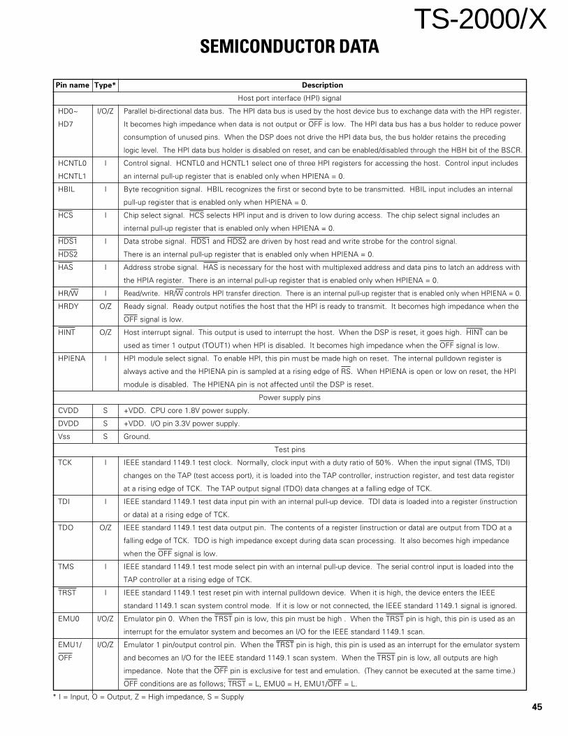
45
TS-2000/X
Pin name Type* Description
Host port interface (HPI) signal
HD0~ I/O/Z Parallel bi-directional data bus. The HPI data bus is used by the host device bus to exchange data with the HPI register.
HD7 It becomes high impedance when data is not output or OFF is low. The HPI data bus has a bus holder to reduce power
consumption of unused pins. When the DSP does not drive the HPI data bus, the bus holder retains the preceding
logic level. The HPI data bus holder is disabled on reset, and can be enabled/disabled through the HBH bit of the BSCR.
HCNTL0 I Control signal. HCNTL0 and HCNTL1 select one of three HPI registers for accessing the host. Control input includes
HCNTL1 an internal pull-up register that is enabled only when HPIENA = 0.
HBIL I Byte recognition signal. HBIL recognizes the first or second byte to be transmitted. HBIL input includes an internal
pull-up register that is enabled only when HPIENA = 0.
HCS I Chip select signal. HCS selects HPI input and is driven to low during access. The chip select signal includes an
internal pull-up register that is enabled only when HPIENA = 0.
HDS1 I Data strobe signal. HDS1 and HDS2 are driven by host read and write strobe for the control signal.
HDS2 There is an internal pull-up register that is enabled only when HPIENA = 0.
HAS I Address strobe signal. HAS is necessary for the host with multiplexed address and data pins to latch an address with
the HPIA register. There is an internal pull-up register that is enabled only when HPIENA = 0.
HR/W I Read/write. HR/W controls HPI transfer direction. There is an internal pull-up register that is enabled only when HPIENA = 0.
HRDY O/Z Ready signal. Ready output notifies the host that the HPI is ready to transmit. It becomes high impedance when the
OFF signal is low.
HINT O/Z Host interrupt signal. This output is used to interrupt the host. When the DSP is reset, it goes high. HINT can be
used as timer 1 output (TOUT1) when HPI is disabled. It becomes high impedance when the OFF signal is low.
HPIENA I HPI module select signal. To enable HPI, this pin must be made high on reset. The internal pulldown register is
always active and the HPIENA pin is sampled at a rising edge of RS. When HPIENA is open or low on reset, the HPI
module is disabled. The HPIENA pin is not affected until the DSP is reset.
Power supply pins
CVDD S +VDD. CPU core 1.8V power supply.
DVDD S +VDD. I/O pin 3.3V power supply.
Vss S Ground.
Test pins
TCK I IEEE standard 1149.1 test clock. Normally, clock input with a duty ratio of 50%. When the input signal (TMS, TDI)
changes on the TAP (test access port), it is loaded into the TAP controller, instruction register, and test data register
at a rising edge of TCK. The TAP output signal (TDO) data changes at a falling edge of TCK.
TDI I IEEE standard 1149.1 test data input pin with an internal pull-up device. TDI data is loaded into a register (instruction
or data) at a rising edge of TCK.
TDO O/Z IEEE standard 1149.1 test data output pin. The contents of a register (instruction or data) are output from TDO at a
falling edge of TCK. TDO is high impedance except during data scan processing. It also becomes high impedance
when the OFF signal is low.
TMS I IEEE standard 1149.1 test mode select pin with an internal pull-up device. The serial control input is loaded into the
TAP controller at a rising edge of TCK.
TRST I IEEE standard 1149.1 test reset pin with internal pulldown device. When it is high, the device enters the IEEE
standard 1149.1 scan system control mode. If it is low or not connected, the IEEE standard 1149.1 signal is ignored.
EMU0 I/O/Z Emulator pin 0. When the TRST pin is low, this pin must be high . When the TRST pin is high, this pin is used as an
interrupt for the emulator system and becomes an I/O for the IEEE standard 1149.1 scan.
EMU1/ I/O/Z Emulator 1 pin/output control pin. When the TRST pin is high, this pin is used as an interrupt for the emulator system
OFF and becomes an I/O for the IEEE standard 1149.1 scan system. When the TRST pin is low, all outputs are high
impedance. Note that the OFF pin is exclusive for test and emulation. (They cannot be executed at the same time.)
OFF conditions are as follows; TRST = L, EMU0 = H, EMU1/OFF = L.
* I = Input, O = Output, Z = High impedance, S = Supply
SEMICONDUCTOR DATA

46
TS-2000/X
CODEC (24 bit) : AK4524 (Control unit IC518)
Block diagram
Control Register I/F
DATTSMUTE
HPFDATT
Audio I/FController
ADC
DAC
3
2
26
1
11
25
28
27
17 16 15
12
13
14
20
4
6
5
23
22
24
19
Clock Gen. & Divider
18 21 8 9 10
AINL
AINR
VCOM
AOUTL+
AOUTL–
AOUTR+
AOUTR–
VD
VT
DGND
PD
LRCK
BICK
SDTO
SDTI
M/S
VREF
VA
AGND
CS CCLK CDTI CIF CLKO XTO XTI XTALE
Pin function
No. Name I/O Function
1 VCOM O Common voltage output pin, VA/2.
Bias voltage os ADC inputs and DAC
outputs.
2 AINR I Rch analog input pin.
3 AINL I Lch analog input pin.
4 VREF I Voltage reference input pin, VA.
Used as a voltage reference by ADC
& DAC, VREF is connected externally
to filtered VA.
5 AGND – Analog ground pin.
6 VA – Analog power supply pin, 4.75~5.25V
7 TEST I Test pin. (Internal pull-down pin)
8 XTO O X’tal output pin.
9 XTI I X’tal/master clock input pin.
10 XTALE I X’tal osc enable pin.
“H” : Enable, “L” : Disable
11 LRCK I/O Input/output channel clock pin.
12 BICK I/O Audio serial data clock pin.
13 SDTO O Audio serial data output pin.
14 SDTI I Audio serial data input pin.
15 CDTI I Control data input pin.
16 CCLK I Control data clock pin.
17 CS I Chip select pin.
18 CIF I Control data I/F format pin.
“H” : CS falling trigger,
“L” : CS rising trigger
19 PD I Power down mode in.
“H” : Power up, “L” : Power down
reset and initialize the control register.
Mixer : TA4101F (TX-RX 1 unit IC6)
Equivalent circuit
3 : OSC in2 : Vcc
8 : Collector1 : IF out
4 : Base
6 : Base
7 : GND5 : Base
RL1 RL2R1
RB1
RB2
R2
RB3
RB4R3
RE1 RE2
R4
Q1 Q2 Q3 Q4
Q5 Q6
No. Name I/O Function
20 M/S I Master/slave mode pin.
“H” : Master mode, “L” : Slave mode
21 CLKO O Master clock output pin.
22 VT – Output buffer power supply pin,
2.7~5.25V.
23 VD – Digital power supply pin, 4.75~5.25V.
24 DGND – Digital ground pin.
25 AOUTL– O Lch negative analog output pin.
26 AOUTL+ O Lch positive analog output pin.
27 AOUTR– O Rch negative analog output pin.
28 AOUTR+ O Rch positive analog output pin.
Note : All input pins except pull-down pins should not be left floating.
SEMICONDUCTOR DATA

47
TS-2000/X
CODEC (16 bit) : AK4518
(Control unit IC522,523)
Block diagram
∆∑Modulator
DecimationFilter
ClockDivider
Serial I/OInterface
CommonVoltage
8xInterpolator
∆∑Modulator
DecimationFilter
∆∑ModulatorLPF
8xInterpolator
∆∑ModulatorLPF
6
5
3
4
2
1
21
19
20
24 22 23 14 13
15
12
11
10
18
17
8
7
16
9AINL
VCML
AINR
VCMR
VRAD
VRDA
VCOM
AOUTL
AOUTR
MCLK
CMODE
LRCK
SCLK
SDTO
SDTI
PWAD
PWDA
DEM1
DEM0
VA AGND VB VD DGND
No. Name I/O Function
17 DEM1 I De-emphasis frequency select pin.
18 DEM0 I De-emphasis frequency select pin.
19 AOUTL O Lch analog output pin.
20 AOUTR O Rch analog output pin.
21 VCOM O Common voltage output pin, 0.45 x VA.
Connect a 4.7µF electrolytic capacitor
and 0.1µF ceramic capacitor between
this pin and AGND.
22 AGND – Analog ground pin.
23 VB – Substrate pin.
24 VA – Analog power supply pin.
Amplifier : UPC2709TB
(TX-RX 2 unit IC405, 415,416, TX-RX 3 unit IC1)
Equivalent circuit
6 : Vcc4 : OUT
2,5 : GND3 : GND
1 : IN
Pin function
No. Name I/O Function
1 VRDA I Voltage reference input pin for DAC, VA.
2 VRAD I Voltage reference input pin for ADC, VA.
3 AINR I Rch analog input pin.
4 VCMR O Rch common voltage output pin,
0.45 x VA. Connect a 4.7µF electrolytic
capacitor and 0.1µF ceramic capacitor
between this pin and AGND.
5 VCML O Lch common voltage output pin,
0.45 x VA. Connect a 4.7µF electrolytic
capacitor and 0.1µF ceramic capacitor
between this pin and AGND.
6 AINL I Lch analog input pin.
7 PWAD I ADC power down mode pin.
“L” : Power down
8 PWDA I DAC power down mode pin.
“L” : Power down
9 MCLK I Master clock input pin.
10 LRCK I Input/output channel clock pin.
11 SCLK I Audio serial data clock pin.
12 SDTO O Audio serial data output pin.
13 DGND – Digital ground pin.
14 VD – Digital power supply pin.
15 SDTI I Audio serial data input pin.
16 CMODE I Master clock select pin.
“H” : 384fs or 512fs, “L” : 256fs
SEMICONDUCTOR DATA

48
TS-2000/X
DAC : M62363FP (TX-RX 1 unit IC14)
Block diagram
8-bit latch 8-bit latch
D0
D1
D2
D3
D4
D5
D6
D7
D8
D9
D10
D11
Addressdecoder
12-bit shift register
7
19
5
6
178
D-Aconverter
D-Aconverter
23242120
18
DI
CLK
RESET
VDD
GND VIN1 VOUT1 VIN8 VOUT8
VDAref
LD
DO
Pin function
No. Symbol Function
8 DI Serial data input terminal.
17 DO Serial data output terminal.
7 CLK Serial clock input terminal.
6 LD LD terminal input high level then latch circuit
data load.
19 RESET Reset terminal.
2 VOUT1 8-bit resolution D-A output.
3 VOUT2
10 VOUT3
11 VOUT4
14 VOUT5
15 VOUT6
22 VOUT7
23 VOUT8
5 VDD Power supply terminal.
20 GND GND terminal.
1 VIN1 D-A converter input terminal.
4 VIN2
9 VIN3
12 VIN4
13 VIN5
16 VIN6
21 VIN7
24 VIN8
18 VDAref D-A converter reference voltage input terminal.
VO = (VIN – VDAref) x n / 256 + VDAref
SEMICONDUCTOR DATA
∑
COMP
IOUT
FSELECTBIT
REFINFS ADJUSTREFOUTDVDD
SELSRC
FREQ0 REG
FREQ1 REGMUX
PhaseAccumulator
(32 bit)
SYNC
SYNC
SYNC
SYNC
MUX
COSROM
10-bitDAC
12
PHASE0 REGPHASE1 REGPHASE2 REGPHASE3 REG
16-bit Data Register
Decode Logic
Serial Register
8 MSBs 8 LSBs
Control RegisterFSELECT/PSEL
Register
DeferRegister
PSEL0BIT
SELSRC
9
FSYNC7
SCLK
8
SDATA11
PSEL0
PSEL1BIT
12
14
PSEL1
16ON-BoardReference
Full-ScaleControl10FSELECT
6MCLK
134DGND
5AVDD
15AGND
13 2
DDS : AD9835 (TX-RX 1 unit IC601~603,
TX-RX 2 unit IC406~408)
Block diagram
Pin function
No. Symbol Function
Analog signal and reference
1 FS ADJUST Full-scale adjust control.
2 REFIN Voltage reference input.
3 REFOUT Voltage reference output.
14 IOUT Current output.
16 COMP Compensation pin.
Power supply
4 DVDD Positive power supply for the digital
section.
5 DGND Digital ground.
13 AGND Analog ground.
15 AVDD Positive power suply fot the analog
section.
Digital interface and control
6 MCLK Digital clock input.
7 SCLK Serial clock, logic input.
8 SDATA Serial data in, logic input.
9 FSYNC Data synchronization signal, logic input.
10 FSELECT Frequency select input.
11 PSEL0 Phase select input.
12 PSEL1

49
TS-2000/X
PLL : LMX2306TMX (TX-RX 2 unit IC401,409~412,414)
PLL : LMX2316TMX (TX-RX 2 unit IC402, TX-RX 3 unit IC5)
Block diagram
14-bitR counter
21-bitData Register
18-bitFunction
Latch
PhaseComp.
LockDetect
FastLock
FoLDMUX18-bit
N counterPrescaler
OSCChargePump
OSCIN
fIN
CLOCKLE
DATA
CPo
FLo
FoLD
Pin description
No. Name I/O Description
1 FLo O FastLock output. For connection of
parallel resistor to the loop filter.
2 CPo O Charge pump output. For connection to a
loop filter for driving the input of an
external VCO.
3 GND – Charge pump ground.
4 GND – Analog ground.
5 fIN I RF prescaler complementary input.
A bypass capacitor should be placed as
close as possible to this pin and be
connected directly to the ground plane.
The complementary input can be left
unbypassed, with some degradation in
RF sensitivity.
6 fIN I RF prescaler input. Small signal input
from the VCO.
7 Vcc1 – Analog power supply voltage input.
Input may range from 2.3V to 5.5V.
Bypass capacitors should be placed as
close as possible to this pin and be
connected directly to the ground plane.
Vcc1 must equal Vcc2.
8 OSCIN I Oscillator input. This input is a CMOS
input with a threshold of approximately
Vcc/2 and an equivalent 100k input
resistance. The oscillator input is driven
from a reference oscillator.
9 GND – Digital ground.
No. Name I/O Description
10 CE I Chip enable. A LOW on CE powers down
the device and will TRI-STATE the charge
pump output. Taking CE HIGH will power
up the device depending on the status of
the power down bit F2.
11 Clock I High impedance CMOS clock input. Data
for the various counters is clocked in on
the rising edge into the 21-bit shift
register.
12 Data I Binary serial data input. Data entered
MSB first. The last two bits are the
control bits. High impedance CMOS input.
13 LE I Load enable CMOS input. When LE goes
high, data stored in the shift registers is
loaded into one of the 3 appropriate
latches (control bit dependent).
14 Fo/LD O Multiplexed output of the RF program-
mable of reference dividers and lock
detect. CMOS output.
15 Vcc2 – Digital power supply voltage input. Input
may range from 2.3V to 5.5V. Bypass
capacitors should be placed as close as
possible to this pin and be connected
directly to the ground plane. Vcc1 must
equal Vcc2.
16 Vp – Power supply for charge pump.
Must be ≥ Vcc.
SEMICONDUCTOR DATA

50
TS-2000/X
DDS : AD9851BRS (TX-RX 3 unit IC4)
Block diagram
6 x REFCLKMultiplier
HighSpeedDDS
10-bitDAC
32-bitTuningWord
Phaseand
ControlWords
Frequency/PhaseData Register
Data Input Register
ParallelLoad
RefClock in
MasterReset
FrequencyUpdate/Data
RegisterReset
Word LoadClock
SerialLoad
DAC RSET
Analogout
Analogin
Clock outClock out
Comparator
+
–
GND+Vs
1 bit x40 Loads
8 bits x5 Loads
Frequency, Phaseand Control Data Input
Pin function
No. Name Function
1~4 D3~D0 8-bit data input. The data port for loading
25~28 D7~D4 the 32-bit frequency and 8-bit phase/control
words. D7 = MSB, D0 = LSB. D7, pin 25,
also serves as the input pin 40-bit serial data
word.
5 PGND 6 x REFCLK multiplier ground connection.
6 PVCC 6 x REFCLK multiplier positive supply
voltage pin.
7 W CLK Word load clock. Rising edge loads the
parallel or serial frequency/phase/control
words asynchronously into the 40-bit input
register.
8 FQ UD Frequency update. Arising edge asynchro-
nously transfers the contents of the 40-bit
input register to be acted upon by the DDS
core. FQ UD should be issued when the
contents of the input register are known to
contain only valid, allowable data.
9 REFCLOCK Reference clock input. CMOS/TTL level
pulse train, direct or via the 6 x REFCLK
multiplier. In direct mode, this is also the
SYSTEM CLOCK. If the 6 x REFCLK multi-
plier is engaged, then the output of the
multiplier is the SYSTEM CLOCK. The rising
edge of the SYSTEM CLOCK initiates
operations.
No. Name Function
10,19 AGND Analog ground. The ground return for the
analog circuitry (DAC and comparator).
11,18 AVDD Positive supply voltage for analog circuitry
(DAC and comparator, pin 18) and bandgap
voltage reference (pin 11).
12 RSET The DAC’s external RSET connection–
nominally a 3.92kΩ resistor to ground for
10mA out. This sets the DAC full-scale
output current available from IOUT and
IOUTB. RSET = 39.93/IOUT.
13 VOUTN Voltage output negative. The comparator’s
“complementary” CMOS logic level output.
14 VOUTP Voltage output positive. The comparator’s
“true” CMOS logic level output.
15 VINN Voltage input negative. The comparator’s
inverting input.
16 VINP Voltage input positive. The comparator’s
noninverting input.
17 DACBP DAC bypass connection. This is he DAC
voltage reference bypass connection
normally NC (no connect) for optimum
SFDR performance.
20 IOUTB The “complementary” DAC output with
same characteristics as IOUT except that
IOUTB = (full-scale output – IOUT). Output
load should equal that of IOUT for best
SFDR performance.
21 IOUT The “true” output of the balanced DAC.
Current is “sourcing” and requires current
to voltage conversion, usually a resistor or
transformer referenced to GND.
IOUT = (full-scale output – IOUTB).
22 RESET Master reset pin, active high, clears DDS
accumulator and phase offset register to
achieve 0Hz and 0° output phase.
Sets programming to parallel mode and
disengages the 6 x REFCLK multiplier.
Reset does mot clear the 40-bit input
register. On power up, asserting RESET
should be the first priority before program-
ming commences.
23 DVDD Positive supply voltage pin for digital circuitry.
24 DGND Digital ground. The ground return pin for the
digital circuitry.
SEMICONDUCTOR DATA

TS-2000/XPARTS LIST
51K : TS-2000 (K) KX : TS-2000X (K)
E : TS-2000 (E) E2 : TS-2000 (E2)
New Parts. indicates safety critical components.Parts without Parts No. are not supplied.Les articles non mentionnes dans le Parts No. ne sont pas fournis.Teile ohne Parts No. werden nicht geliefert.
L : Scandinavia K : USA P : CanadaY : PX (Far East, Hawaii) T : England E : EuropeY : AAFES (Europe) X : Australia M: Other Areas
TS-2000/X
New Desti-parts nationRef. No. Address Parts No. Description New Desti-
parts nationRef. No. Address Parts No. Description
1 2A A01-2176-01 CABINET (UPPER)2 1D A01-2177-01 CABINET (BOTTOM)3 2C A10-4017-01 CHASSIS4 1B A11-0417-01 SUB CHASSIS5 1F A22-2502-21 SUB PANEL
6 2E A62-0771-03 PANEL ASSY
7 1C B09-0355-05 CAP8 2E B10-2608-02 FRONT GLASS10 1I B42-7003-04 RATING LABEL (DC CORD) E,E218 2E B43-1222-04 BADGE12 1J B46-0310-03 WARRANTY CARD E,E2
12 1J B46-0469-10 WARRANTY CARD K,KX13 1J B52-0614-00 SCHEMATIC DIAGRAM14 1J B52-0616-00 SCHEMATIC DIAGRAM15 1J B52-0617-00 SCHEMATIC DIAGRAM27 1J B52-0618-00 SCHEMATIC DIAGRAM
28 1J B59-1777-00 PAMPHLET E,E216 1J B62-1221-10 INSTRUCTION MANUAL (ENGLISH) K,KX,E16 1J B62-1222-00 INSTRUCTION MANUAL (FRENCH) E16 1J B62-1223-10 INSTRUCTION MANUAL (SPANISH) E216 1J B62-1224-00 INSTRUCTION MANUAL (GERMAN) E
16 1J B62-1225-00 INSTRUCTION MANUAL (ITALIAN) E16 1J B62-1226-00 INSTRUCTION MANUAL (DUTCH) E17 2C B72-1641-04 MODEL NAME PLATE K17 2C B72-1642-14 MODEL NAME PLATE E,E217 2C B72-1879-04 MODEL NAME PLATE KX
19 2C E04-0167-05 RF COAXIAL PECEPTACLE (M)20 2C E04-0170-05 RF COAXIAL RECEPTACLE (N)21 2I E07-0751-05 DIN PLUG (7P ACC)22 2I E07-0851-05 DIN PLUG (8P ACC)- E07-0852-15 ROUND PLUG
24 2I E07-1351-05 DIN PLUG (13P ACC)25 2C E23-1164-04 EARTH LUG (ANT)26 1I E30-3157-15 DC CORD27 2C,3C,2F E37-0866-05 FLAT CABLE (X57-605 CN26,800)28 1B E37-0867-05 FLAT CABLE (X57-606B CN501)
29 3C E37-0868-05 FLAT CABLE (X53 CN6)30 1C E37-0869-05 FLAT CABLE (X53 CN504)31 2B E37-0870-05 FLAT CABLE (X57-606A CN12)32 1C E37-0871-05 FLAT CABLE (X45A CN9)33 2B E37-0872-05 FLAT CABLE (X57-606A CN14)
34 3B E37-0873-05 LEAD WIRE WITH TERMINAL (X45A CN203, +B)35 3B E37-0874-05 LEAD WIRE WITH TERMINAL (X45A CN204, GND)- E37-0875-05 LEAD WIRE WITH MINIPIN PLUG (X57-606B CN502)- E37-0876-05 LEAD WIRE WITH MINIPIN PLUG (X57-606C CN506)- E37-0877-05 LEAD WIRE WITH MINIPIN PLUG (X57-606A CN8,13)
- E37-0878-05 LEAD WIRE WITH MINIPIN PLUG (X51 CN20, HF RX)- E37-0879-05 LEAD WIRE WITH MINIPIN PLUG (X45A CN1, HFTX)- E37-0880-05 LEAD WIRE WITH MINIPIN PLUG (X57-606A CN6)- E37-0881-05 LEAD WIRE WITH MINIPIN PLUG (X45A CN2, 14TX)- E37-0882-05 LEAD WIRE WITH MINIPIN PLUG (X51 CN21, 14RX)
- E37-0883-05 LEAD WIRE WITH MINIPIN PLUG (X57-606A CN2,3)- E37-0886-05 LEAD WIRE WITH CONNECTOR (X53 CN505)
- E37-0887-05 LEAD WIRE WITH CONNECTOR (X53 CN503)- E37-0888-05 LEAD WIRE WITH CONNECTOR (X57-606A CN9)- E37-0889-05 LEAD WIRE WITH CONNECTOR (X57-605A CN31,32)- E37-0890-05 LEAD WIRE WITH CONNECTOR (X57-606A CN10)50 2C E37-0891-05 LEAD WIRE WITH CONNECTOR (EXT AT)
- E37-0897-05 LEAD WIRE WITH CONNECTOR (X57-607 CN1) KX- E37-0898-05 LEAD WIRE WITH CONNECTOR (X57-607 CN5) KX53 1B E37-0946-05 FLAT CABLE (X57-606B CN533)54 3C E37-0947-05 FLAT CABLE (X53 CN1)55 2F E37-0948-05 FLAT CABLE (X54 CN1)
- E37-0951-05 LEAD WIRE WITH MINIPIN PLUG (X51 CN4)- E37-0952-05 LEAD WIRE WITH MINIPIN PLUG (X51 CN12,13)- E37-0953-05 LEAD WIRE WITH MINIPIN PLUG (X57-606A CN18)- E37-0957-05 LEAD WIRE WITH CONNECTOR (X51 CN10)- E37-0958-05 LEAD WIRE WITH CONNECTOR (X51 CN9)
61 3B E37-0959-05 LEAD WIRE WITH CONNECTOR (SP)62 3C E37-0963-05 FLAT CABLE (X57-607 CN6) KX
65 1I,2I F05-2531-05 FUSE (BLADE) 25A/32V66 2I F06-4027-05 FUSE (BLADE) 4A/32V67 1C F07-1849-05 COVER68 1C F09-0453-05 CAP69 3C F09-0471-05 FANMOTOR
70 2B F10-2328-02 SHIELDING PLATE71 2B F10-2330-13 SHIELDING COVER72 3B F10-2366-03 SHIELDING PLATE KX73 2B F10-2398-04 SHIELDING COVER74 3G F12-0463-04 SHIELDIBG SHEET
- F15-0700-04 SHIELDING PLATE K,E,E275 1A F20-1185-04 INSULATING SHEET76 3B F29-0014-05 INSULATING BUSH
78 3E G02-0505-05 KNOB SPRING79 1C G02-0570-04 FLAT SPRING- G02-0729-14 FLAT SPRING (1.2G, A25) KX80 3E G02-0854-03 FLAT SPRING81 2A G02-0875-04 EARTH SPRING
82 2F G02-0879-04 EARTH SPRING83 3B G02-0881-04 FLAT SPRING84 3E G09-0405-05 KNOB SPRING110 2E G10-0789-04 FIBROUS SHEET85 3E G10-1258-04 FIBROUS SHEET
86 2A,3A G10-1277-04 FIBROUS SHEET87 1F G10-1278-04 FIBROUS SHEET88 3D G10-1281-04 FIBROUS SHEET98 2F G11-2521-04 SHEET89 3C G11-2588-04 RUBBER SHEET
90 1I G11-2698-04 SHEET91 2F G11-4035-04 SHEET92 2F G11-4036-04 SHEET93 2F G11-4037-14 SHEET94 2F G11-4038-04 SHEET
95 2F G11-4039-14 SHEET96 2F G11-4041-04 SHEET97 3C G11-4042-04 SHEET108 2F G11-4045-04 SHEET99 2E G13-1775-13 CUSHION
TS-2000/X

TS-2000/XPARTS LIST
52K : TS-2000 (K) KX : TS-2000X (K)
E : TS-2000 (E) E2 : TS-2000 (E2)
Ref. No. Address Parts No. Description Ref. No. Address Parts No. DescriptionNew Desti-parts nation
New Desti-parts nation
100 3B G13-1793-04 CUSHION101 3A G13-1855-04 CUSHION102 1C G13-1856-04 CUSHION103 1D G13-1868-04 CUSHION104 1G G13-1869-05 CONDUCTIVE CUSHION
105 1H G13-1870-05 CONDUCTIVE CUSHION106 1H G13-1871-05 CONDUCTIVE CUSHION107 3H G13-1872-05 CONDUCTIVE CUSHION- G13-1877-05 CONDUCTIVE CUSHION KX- G13-1878-05 CONDUCTIVE CUSHION KX
109 2J H52-1509-02 ITEM CARTON CASE K109 2J H52-1712-02 ITEM CARTON CASE KX109 2J H52-1773-02 ITEM CARTON CASE E,E2
111 1D J02-0440-04 FOOT112 3A,2D J02-0441-05 FOOT113 2D J02-0442-04 FOOT114 1D J02-0475-05 FOOT115 3B J21-8414-04 HARDWARE FIXTURE
116 1E J31-0141-04 COLLAR117 3E J39-0638-04 SPACER- J61-0307-05 BAND
120 2A K01-0420-05 HANDLE121 3E K21-1104-03 KNOB122 2E K29-5391-02 KEY TOP123 2F K29-5392-12 KEY TOP124 2F K29-5393-12 KEY TOP
125 2F K29-5394-12 KEY TOP126 3E K29-5395-04 KNOB RING127 3E K29-5396-03 KNOB128 3E K29-5397-13 KNOB129 3E K29-5398-03 KNOB
130 3E K29-5399-03 KNOB
- L79-1407-05 LINE FILTER133 2I L79-1408-05 LINE FILTER (WITH BAND) E,E2
A 1F N14-0569-04 CIRCULAR NUTB 2C N15-1040-46 FLAT WASHERC 3E N19-0670-05 SPECIAL WASHERD 1F N19-0673-05 SPECIAL WASHERE 2A,1D N33-3006-45 OVAL HEAD MACHINE SCREW
F 1D,2D N35-3008-41 BINDING HEAD MACHINE SCREWG 3C N35-3020-46 BINDING HEAD MACHINE SCREWH 2C N35-4010-46 BINDING HEAD MACHINE SCREWJ 2A N67-2608-46 PAN HEAD SEMS SCREW WK 2A,3B N68-4006-46 PAN HEAD SEMS SCREW A
L 1E,2F N87-2606-46 BRAZIER HEAD TAPTITE SCREWM 2B,2F N87-2608-46 BRAZIER HEAD TAPTITE SCREWN 3E N90-3008-46 TP HEAD MACHINE SCREW135 1I N99-2024-05 SCREW SET
- S50-1406-05 TACT SWITCH
139 3B T07-0252-35 SPEAKER140 1I T91-0352-15 MICROPHONE
142 2F W02-1836-05 ENCODER143 1F W02-3619-05 ENCODER- W09-0873-05 LITHIUM CELL (X57-605 A)
146 2E 212-2017-05 HEAT-PROOF TUBE
C1 CK73FB1E104K CHIP C 0.10UF KC2 CK73FB1H103K CHIP C 0.010UF KC3 CK73FB1E104K CHIP C 0.10UF KC4 CK73FB1H103K CHIP C 0.010UF KC5 CK73FB1H102K CHIP C 1000PF K
C6 CK73FB1E104K CHIP C 0.10UF KC7 CK73FB1C105K CHIP C 1.0UF KC8,9 CK73FB1E104K CHIP C 0.10UF KC10 CK73FB1C105K CHIP C 1.0UF KC11 CK73FB1H102K CHIP C 1000PF K
C12 CE04EW1E100M ELECTRO 10UF 25WVC13 CK73FB1E104K CHIP C 0.10UF KC14 CK73FB1H102K CHIP C 1000PF KC15 CK73FB1E104K CHIP C 0.10UF KC17 CK73FB1E104K CHIP C 0.10UF K
C20 CC73FCH1H331J CHIP C 330PF JC21 CK73FB1E104K CHIP C 0.10UF KC22 CK73FB1H102K CHIP C 1000PF KC24 CK73FB1E104K CHIP C 0.10UF KC25 CK73FB1C105K CHIP C 1.0UF K
C26 CC73FCH1H390J CHIP C 39PF JC27 CC73FCH1H470J CHIP C 47PF JC29,30 CK73EB1H104K CHIP C 0.10UF KC31 C93-0569-05 CHIP C 56PF JC32 CK73FB1H102K CHIP C 1000PF K
C33 CE04EW1E100M ELECTRO 10UF 25WVC34 CE04EW1E470M ELECTRO 47UF 25WVC35 CK73FB1E104K CHIP C 0.10UF KC36 CK73FB1C105K CHIP C 1.0UF KC37 CK73FB1H102K CHIP C 1000PF K
C38 CK73FB1E104K CHIP C 0.10UF KC39 CK73FB1H102K CHIP C 1000PF KC40 CK73FB1C105K CHIP C 1.0UF KC41,42 CK73FB1E104K CHIP C 0.10UF KC43 CK73FB1H103K CHIP C 0.010UF K
C44 CK73FB1C105K CHIP C 1.0UF KC45 CK73FB1H103K CHIP C 0.010UF KC46 C93-0568-05 CHIP C 47PF JC47 CM73F2H271J CHIP C 270PF JC48 CM73F2H391J CHIP C 390PF J
C49-56 C93-0608-05 CHIP C 2700PF KC57,58 C93-0572-05 CHIP C 100PF JC59,60 C93-0568-05 CHIP C 47PF JC61 CM73F2H331J CHIP C 330PF JC63 C93-0555-05 CHIP C 5.0PF C
C67 C93-0555-05 CHIP C 5.0PF CC68 CK73FB1E104K CHIP C 0.10UF KC69 CK73FB1H102K CHIP C 1000PF KC70 CE04EW1E100M ELECTRO 10UF 25WVC71 CK73FB1H103K CHIP C 0.010UF K
C72 CK73FB1E104K CHIP C 0.10UF KC73 CK73FB1H102K CHIP C 1000PF KC74 CK73FB1E104K CHIP C 0.10UF KC79 C90-4089-05 ELECTRO 220UF 25WVC101 C93-0567-05 CHIP C 39PF J
C102 C93-0560-05 CHIP C 10PF DC104 C93-0572-05 CHIP C 100PF JC106 C93-0572-05 CHIP C 100PF J
FINAL UNIT (X45-360X-XX) 0-11 : K,KX 2-71 : E,E2
TS-2000/X
FINAL UNIT (X45-360X-XX)

TS-2000/XPARTS LIST
53K : TS-2000 (K) KX : TS-2000X (K)
E : TS-2000 (E) E2 : TS-2000 (E2)
Ref. No. Address Parts No. Description Ref. No. Address Parts No. DescriptionNew Desti-parts nation
New Desti-parts nation
C107 CM73F2H271J CHIP C 270PF JC108 CM73F2H221J CHIP C 220PF JC110 CM73F2H271J CHIP C 270PF JC111 CM73F2H221J CHIP C 220PF JC117,118 CM73F2H151J CHIP C 150PF J
C125 CK73EF1V225Z CHIP C 2.2UF ZC127 CK73FB1H102K CHIP C 1000PF KC130,131 CM73F2H151J CHIP C 150PF JC132 CC73FSL1H471J CHIP C 470PF JC133 CK73FB1H103K CHIP C 0.010UF K
C135 CK73FB1E104K CHIP C 0.10UF KC138 CK73FB1H102K CHIP C 1000PF KC139,140 CC73FSL1H331J CHIP C 330PF JC141 CK73FB1H102K CHIP C 1000PF KC142 CK73FB1E104K CHIP C 0.10UF K
C143 CK73FB1H471K CHIP C 470PF KC144 CE04EW1E100M ELECTRO 10UF 25WVC145 CK73FB1H471K CHIP C 470PF KC146 CK73FB1E104K CHIP C 0.10UF KC147 CK73FB1H102K CHIP C 1000PF K
C148 CC73FSL1H471J CHIP C 470PF JC149 CK73FB1H103K CHIP C 0.010UF KC150 CM73F2H680J CHIP C 68PF JC151,152 C93-0554-05 CHIP C 4.0PF CC153 CM73F2H680J CHIP C 68PF J
C154,155 C93-0554-05 CHIP C 4.0PF CC157 CM73F2H200J CHIP C 20PF JC158,159 C93-0603-05 CHIP C 1000PF KC160 C93-0560-05 CHIP C 10PF DC161,162 CC73FCH1H100D CHIP C 10PF D
C201,202 CK73FB1H102K CHIP C 1000PF KC203,204 CK73FB1H103K CHIP C 0.010UF KC205 C91-2691-05 CERAMIC 470PF 250WVC206 CK73FB1H103K CHIP C 0.010UF KC207 CE04EW1E471M ELECTRO 470UF 25WV
C208 CK73FB1H103K CHIP C 0.010UF KC209 CK73FB1E104K CHIP C 0.10UF KC210 CK73FB1H103K CHIP C 0.010UF KC211 CK73FB1E104K CHIP C 0.10UF KC212 CK73FB1H103K CHIP C 0.010UF K
C213 CE04EW1E471M ELECTRO 470UF 25WVC214 CK73FB1H103K CHIP C 0.010UF KC215 CK73FB1E104K CHIP C 0.10UF KC216 CK73FB1H102K CHIP C 1000PF KC217-221 CK73FB1E104K CHIP C 0.10UF K
C222,223 CE04EW1E100M ELECTRO 10UF 25WVC224 CE04EW1E102M ELECTRO 1000UF 25WVC225,226 CK73FB1E104K CHIP C 0.10UF KC227 C90-2021-05 ELECTRO 10UF 25WVC228,229 CK73FB1E104K CHIP C 0.10UF K
C230 CE04EW1E100M ELECTRO 10UF 25WVC231 CK73FB1E104K CHIP C 0.10UF KC232-234 CK73FB1H103K CHIP C 0.010UF KC235,236 CK73FB1H102K CHIP C 1000PF KC237 CK73FB1H103K CHIP C 0.010UF K
C238 CK73FB1H102K CHIP C 1000PF KC239 CE04EW1E470M ELECTRO 47UF 25WVC240-244 CK73FB1H102K CHIP C 1000PF KC250 CE04EW1E471M ELECTRO 470UF 25WVC251 CK73FB1E104K CHIP C 0.10UF K
C252 CC73FCH1H470J CHIP C 47PF JC253,254 CE04EW1C101M ELECTRO 100UF 16WVC255 CK73FB1H103K CHIP C 0.010UF KC256 CE04EW1HR22M ELECTRO 0.22UF 50WVC259,260 CM73F2H331J CHIP C 330PF J
C262 CK73EF1V225Z CHIP C 2.2UF ZC263 CK73FB1E104K CHIP C 0.10UF KC264 CK73FB1H102K CHIP C 1000PF KC265 CK73FB1H103K CHIP C 0.010UF KC270 C93-0561-05 CHIP C 12PF J
C271 C93-0565-05 CHIP C 27PF JC501,502 CK45FB1H103K CERAMIC 0.010UF KC511,512 CK45FB1H103K CERAMIC 0.010UF KC801-803 CK73FB1E104K CHIP C 0.10UF KC804 CK73FB1H102K CHIP C 1000PF K
C805,806 C91-3115-05 HV CAP 10PF 2KVC807 CK73FB1E104K CHIP C 0.10UF KC808,809 CK73FB1H103K CHIP C 0.010UF KC810-815 C91-3115-05 HV CAP 10PF 2KVC816-821 CK73FB1H103K CHIP C 0.010UF K
C822-827 C91-3115-05 HV CAP 10PF 2KVC828-833 CK73FB1H103K CHIP C 0.010UF KC834,835 C91-3115-05 HV CAP 10PF 2KVC836 C91-3126-05 HV CAP 10PF 3KVC837-842 CK73FB1H103K CHIP C 0.010UF K
C843 C91-3126-05 HV CAP 10PF 3KVC844 C91-3127-05 HV CAP 18PF 3KVC845-850 CK73FB1H103K CHIP C 0.010UF KC851,852 C91-3127-05 HV CAP 18PF 3KVC853-858 CK73FB1H103K CHIP C 0.010UF K
C859 C91-3127-05 HV CAP 18PF 3KVC860-865 CK73FB1H103K CHIP C 0.010UF KC866-869 C91-3123-05 HV CAP 150PF 3KVC870-875 CK73FB1H103K CHIP C 0.010UF KC876,877 C91-3123-05 HV CAP 150PF 3KV
C878-883 CK73FB1H103K CHIP C 0.010UF KC884-887 C91-3123-05 HV CAP 150PF 3KVC888 CK73FB1E104K CHIP C 0.10UF KC890,891 C91-3127-05 HV CAP 18PF 3KVC901 CC73FCH1H470J CHIP C 47PF J
C903 CE04EW1E470M ELECTRO 47UF 25WVC904,905 CK73FB1H471K CHIP C 470PF KC906,907 CK73FB1H103K CHIP C 0.010UF KC908,909 CK73FB1H471K CHIP C 470PF KC911,912 CK73FB1H471K CHIP C 470PF K
C914 CK73FB1C105K CHIP C 1.0UF KC915 CC73FCH1H101J CHIP C 100PF JC916 CK73FB1H103K CHIP C 0.010UF KC919,920 CK73FB1H471K CHIP C 470PF KC921 CK73FB1H103K CHIP C 0.010UF K
C922 CK73FB1C105K CHIP C 1.0UF KC924 CK73FB1H103K CHIP C 0.010UF KC926 CK73FB1H471K CHIP C 470PF KC928 CE04EW1E100M ELECTRO 10UF 25WVC931 CC73FCH1H180J CHIP C 18PF J
C933 CE04EW1C470M ELECTRO 47UF 16WVC934,935 CK73FB1H471K CHIP C 470PF KC936,937 CM73F2H330J CHIP C 33PF JC938 CK73FB1H103K CHIP C 0.010UF KC940 CK73FB1H471K CHIP C 470PF K
FINAL UNIT (X45-360X-XX)

TS-2000/XPARTS LIST
54K : TS-2000 (K) KX : TS-2000X (K)
E : TS-2000 (E) E2 : TS-2000 (E2)
Ref. No. Address Parts No. Description Ref. No. Address Parts No. DescriptionNew Desti-parts nation
New Desti-parts nation
C941,942 CK73FB1H103K CHIP C 0.010UF KC943 C93-0564-05 CHIP C 22PF JC944 CE04EW1E100M ELECTRO 10UF 25WVC945,946 CK73FB1H471K CHIP C 470PF KC947 C93-0564-05 CHIP C 22PF J
C948 CK73FB1H103K CHIP C 0.010UF KC949,950 CM73F2H330J CHIP C 33PF JC952,953 CK73FB1H471K CHIP C 470PF KC955 CE04EW1E100M ELECTRO 10UF 25WVC956 CK73FB1H103K CHIP C 0.010UF K
C958 CK73FB1E104K CHIP C 0.10UF KC959 CE04NW1E470M ELECTRO 47UF 25WVC960,961 CM73F2H390J CHIP C 39PF JC962 CK73FB1H471K CHIP C 470PF KC963 CK73FB1H103K CHIP C 0.010UF K
C964 CM73F2H040D CHIP C 4.0PF DC965 CE04EW1E100M ELECTRO 10UF 25WVC966 CK73FB1H103K CHIP C 0.010UF KC967 CK73FB1H471K CHIP C 470PF KC968 C93-0599-05 CHIP C 470PF K
C969 CK73FB1H471K CHIP C 470PF KC970 CK73FB1H103K CHIP C 0.010UF KC971 CK73FB1H471K CHIP C 470PF KC973,974 CK73FB1H471K CHIP C 470PF KC976 CK73FB1H471K CHIP C 470PF K
C977 C93-0599-05 CHIP C 470PF KC978 C93-0559-05 CHIP C 9.0PF DC980 C93-0555-05 CHIP C 5.0PF CC981 CC73FCH1H471J CHIP C 470PF JC982 CM73F2H120J CHIP C 12PF J
C983 C93-0553-05 CHIP C 3.0PF CC985 C93-0566-05 CHIP C 33PF JC987 C93-0562-05 CHIP C 15PF JC989-991 CC73FCH1H101J CHIP C 100PF JC992 CM73F2H240J CHIP C 24PF J
C993 C93-0558-05 CHIP C 8.0PF DC994 CM73F2H060D CHIP C 6.0PF DC995 C93-0566-05 CHIP C 33PF JTC101,102 C05-0309-05 CERAMIC TRIMMER CAP (40P)TC901 C05-0030-15 CERAMIC TRIMMER CAP (20P)
CN1,2 E04-0154-05 PIN SOCKETCN3 E23-0996-05 TEST TERMINALCN4 E04-0154-05 PIN SOCKETCN5 E40-3240-05 PIN ASSYCN8 E40-3237-05 PIN ASSY
CN9 E40-6078-05 FLAT CABLE CONNECTORCN10 E40-5764-05 FLAT CABLE CONNECTORCN11,12 E23-0996-05 TEST TERMINALCN14 E23-0996-05 TEST TERMINALCN15 E40-3256-05 PIN ASSY
CN16 E40-3254-05 PIN ASSYCN17 E23-0996-05 TEST TERMINALCN22 E40-3246-05 PIN ASSYCN27 E40-3238-05 PIN ASSYCN102,103 E23-0996-05 TEST TERMINAL
CN203,204 E23-1116-05 RELAY TERMINALCN801,802 E04-0154-05 PIN SOCKETCN901 E04-0190-05 PIN SOCKETCN902 E40-5765-05 FLAT CABLE CONNECTORCN903,904 E23-1116-05 RELAY TERMINAL
CN905 E04-0190-05 PIN SOCKETCN906 E23-0486-05 TERMINALCN907-909 E23-0996-05 TEST TERMINALW1 E37-0975-15 LEAD WIRE WITH TERMINAL
F1 F53-0093-05 FUSEF2 F06-4027-05 FUSE (BLADE) 4A/32V
CN6,7 J13-0410-05 FUSE HOLDER
- L92-0105-05 TROIDAL CORE- L92-0412-05 TROIDAL CORE E,E2L1 L40-4705-34 SMALL FIXED INDUCTOR (47UH)L2 L40-1095-34 SMALL FIXED INDUCTOR (1UH)L3 L33-0699-05 CHOKE COIL
L4 L40-4705-34 SMALL FIXED INDUCTOR (47UH)L5 L39-1255-05 TOROIDAL COILL6 L33-0699-05 CHOKE COILL7 L39-1452-05 TOROIDAL COILL8 L92-0131-05 FERRITE CHIP
L9,10 L33-0699-05 CHOKE COILL11 L39-1434-05 TOROIDAL COILL13 L39-1434-05 TOROIDAL COILL14-16 L33-0699-05 CHOKE COILL17 L39-1451-05 TOROIDAL COIL
L18 L39-1437-05 TOROIDAL COILL21 L34-1231-15 AIR-CORE COILL23 L40-4795-34 SMALL FIXED INDUCTOR (4.7UH)L24 L33-0617-15 CHOKE COILL25 L33-0651-05 CHOKE COIL
L26 L40-4795-34 SMALL FIXED INDUCTOR (4.7UH)L27 L39-1450-05 TOROIDAL COILL29 L39-1450-05 TOROIDAL COILL30-33 L92-0149-05 FERRITE CHIPL101,102 L34-0895-05 AIR-CORE COIL
L103,104 L34-1058-05 AIR-CORE COILL105,106 L34-1177-05 AIR-CORE COILL107,108 L34-0908-05 AIR-CORE COILL109 L34-1359-05 AIR-CORE COILL111,112 L40-1095-34 SMALL FIXED INDUCTOR (1UH)
L114 L92-0149-05 FERRITE CHIPL115 L34-4652-05 AIR-CORE COILL116 L34-4656-05 AIR-CORE COILL117 L34-1185-05 AIR-CORE COILL118 L34-4652-05 AIR-CORE COIL
L119 L34-4653-05 AIR-CORE COILL120 L34-4402-05 AIR-CORE COILL121,122 L34-0452-05 AIR-CORE COILL124,125 L92-0149-05 FERRITE CHIPL126 L34-4658-05 AIR-CORE COIL
L127 L92-0149-05 FERRITE CHIPL201,202 L40-4705-34 SMALL FIXED INDUCTOR (47UH)L205 L40-1001-12 SMALL FIXED INDUCTORL206,207 L40-1005-34 SMALL FIXED INDUCTOR (10UH)L208 L40-4705-34 SMALL FIXED INDUCTOR (47UH)
L209 L40-1001-12 SMALL FIXED INDUCTORL210 L40-1095-34 SMALL FIXED INDUCTOR (1UH)L211 L92-0131-05 FERRITE CHIPL501,502 L39-0421-04 COILL801 L40-1001-12 SMALL FIXED INDUCTOR
L802,803 L39-1441-05 TOROIDAL COIL
FINAL UNIT (X45-360X-XX)

TS-2000/XPARTS LIST
55K : TS-2000 (K) KX : TS-2000X (K)
E : TS-2000 (E) E2 : TS-2000 (E2)
Ref. No. Address Parts No. Description Ref. No. Address Parts No. DescriptionNew Desti-parts nation
New Desti-parts nation
L804 L39-1440-05 TOROIDAL COILL805-807 L40-4705-34 SMALL FIXED INDUCTOR (47UH)L808 L34-4633-05 AIR-CORE COILL809-811 L40-4705-34 SMALL FIXED INDUCTOR (47UH)L812 L34-4630-05 AIR-CORE COIL
L813-815 L40-4705-34 SMALL FIXED INDUCTOR (47UH)L816 L34-4490-05 AIR-CORE COILL817-819 L40-4705-34 SMALL FIXED INDUCTOR (47UH)L820 L34-4490-05 AIR-CORE COILL821-823 L40-4705-34 SMALL FIXED INDUCTOR (47UH)
L824 L34-4629-05 AIR-CORE COILL825-827 L40-4705-34 SMALL FIXED INDUCTOR (47UH)L828 L34-4490-05 AIR-CORE COILL829-831 L40-4705-34 SMALL FIXED INDUCTOR (47UH)L832 L34-4490-05 AIR-CORE COIL
L833-835 L40-4705-34 SMALL FIXED INDUCTOR (47UH)L852,853 L39-1441-05 TOROIDAL COILL854 L39-1440-05 TOROIDAL COILL855 L34-1177-05 AIR-CORE COILL901 L40-1085-34 SMALL FIXED INDUCTOR (100NH)
L902 L92-0149-05 FERRITE CHIPL903 L40-1095-34 SMALL FIXED INDUCTOR (1UH)L904 L92-0149-05 FERRITE CHIPL905 L34-0895-05 AIR-CORE COILL906 L34-0742-05 AIR-CORE COIL
L907 L92-0149-05 FERRITE CHIPL909 L34-0742-05 AIR-CORE COILL910 L34-1185-05 AIR-CORE COILL911 L40-1085-34 SMALL FIXED INDUCTOR (100NH)L912 L34-0742-05 AIR-CORE COIL
L913 L92-0149-05 FERRITE CHIPL915 L34-1232-15 AIR-CORE COILL916 L34-1231-15 AIR-CORE COILL917 L34-1239-05 AIR-CORE COILL918,919 L34-1185-05 AIR-CORE COIL
L921,922 L34-1185-05 AIR-CORE COILL923 L34-4617-15 AIR-CORE COILL924 L34-1239-05 AIR-CORE COILL926 L40-2275-34 SMALL FIXED INDUCTOR (22NH)L927-931 L40-1085-34 SMALL FIXED INDUCTOR (100NH)
L932 L34-4617-15 AIR-CORE COIL
CN803,804 R92-1061-05 JUMPER REST 0 OHMR1,2 RK73FB2A101J CHIP R 100 J 1/10WR3 RK73FB2A150J CHIP R 15 J 1/10WR4 RK73FB2A681J CHIP R 680 J 1/10WR5 RK73FB2A332J CHIP R 3.3K J 1/10W
R6 RK73FB2A681J CHIP R 680 J 1/10WR7 RK73FB2A152J CHIP R 1.5K J 1/10WR8 RK73FB2A471J CHIP R 470 J 1/10WR9 RK73FB2A100J CHIP R 10 J 1/10WR10 R92-0670-05 CHIP R 0 OHM
R11 RK73FB2A221J CHIP R 220 J 1/10WR12 RK73FB2A391J CHIP R 390 J 1/10WR13 RK73FB2A471J CHIP R 470 J 1/10WR14 R92-2021-05 CHIP R 2.2 J 1/2WR15 RK73EB2B221J CHIP R 220 J 1/8W
R16-19 RK73FB2A1R0J CHIP R 1.0 J 1/10WR20,21 RK73FB2A470J CHIP R 47 J 1/10WR24 R92-1213-05 CHIP R 100 J 1/2W
R25 RK73FB2A820J CHIP R 82 J 1/10WR26 RK73FB2A270J CHIP R 27 J 1/10WR27 R92-2018-05 CHIP R 560 J 1/2WR30 R92-1318-05 CHIP R 100 J 1WR31,32 R92-2673-05 RESISTOR 1.0
R33,34 R92-3511-05 RESISTOR 8.2R35-40 RK73EB2E1R0J CHIP R 1.0 J 1/4WR41,42 R92-1240-05 CHIP R 10 J 1/4WR43 RK73FB2A331J CHIP R 330 J 1/10WR44 RS14DB3A4R7J FL-PROOF RS 4.7 J 1W
R45,46 RS14DB3D390J FL-PROOF RS 39 J 2WR101 R92-1318-05 CHIP R 100 J 1WR102 RS14DB3A100J FL-PROOF RS 10 J 1WR103 RS14DB3F101J FL-PROOF RS 100 J 3WR106 R92-1213-05 CHIP R 100 J 1/2W
R107 R92-1212-05 CHIP R 27 J 1/2WR108 RK73FB2A100J CHIP R 10 J 1/10WR109 RK73FB2A331J CHIP R 330 J 1/10WR110 RK73FB2A561J CHIP R 560 J 1/10WR111 R92-2559-05 RESISTOR 12
R201 RK73FB2A472J CHIP R 4.7K J 1/10WR202 R92-2536-05 CHIP R 2.2 J 1/4WR203 RK73FB2A472J CHIP R 4.7K J 1/10WR204 R92-1259-05 CHIP R 18 J 1/2WR205 RK73FB2A102J CHIP R 1.0K J 1/10W
R206 RK73FB2A100J CHIP R 10 J 1/10W K,KXR207 RK73FB2A333J CHIP R 33K J 1/10WR208 RK73FB2A102J CHIP R 1.0K J 1/10WR209-212 RK73FB2A101J CHIP R 100 J 1/10WR213 R92-2021-05 CHIP R 2.2 J 1/2W
R214 R92-0679-05 CHIP R 0 OHMR216,217 R92-0670-05 CHIP R 0 OHMR218 RK73FB2A101J CHIP R 100 J 1/10WR219 RK73FB2A681J CHIP R 680 J 1/10WR220 RK73FB2A100J CHIP R 10 J 1/10W
R221 RK73FB2A4R7J CHIP R 4.7 J 1/10WR222 R92-0679-05 CHIP R 0 OHMR501,502 RS14DB3F820J FL-PROOF RS 82 J 3WR901 RK73FB2A563J CHIP R 56K J 1/10WR902 R92-0670-05 CHIP R 0 OHM
R903 RK73FB2A470J CHIP R 47 J 1/10WR904 RK73FB2A274J CHIP R 270K J 1/10WR906 R92-0670-05 CHIP R 0 OHMR907 RK73FB2A332J CHIP R 3.3K J 1/10WR908 R92-0670-05 CHIP R 0 OHM
R909 RK73FB2A470J CHIP R 47 J 1/10WR910 RK73FB2A183J CHIP R 18K J 1/10WR911 RK73FB2A221J CHIP R 220 J 1/10WR912 R92-1221-05 CHIP R 82 J 1/4WR913 RK73FB2A391J CHIP R 390 J 1/10W
R914 R92-1261-05 CHIP R 150 J 1/2WR915 R92-1253-05 CHIP R 82 J 1/2WR916,917 RK73FB2A681J CHIP R 680 J 1/10WR918 R92-1253-05 CHIP R 82 J 1/2WR919-922 RK73FB2A183J CHIP R 18K J 1/10W
R923,924 RK73FB2A220J CHIP R 22 J 1/10WR925 RK73FB2A390J CHIP R 39 J 1/10WR928 R92-0679-05 CHIP R 0 OHMVR1 R12-6730-05 TRIMMING POT. (220)VR2 R12-6737-05 TRIMMING POT. (3.3K)
FINAL UNIT (X45-360X-XX)

TS-2000/XPARTS LIST
56K : TS-2000 (K) KX : TS-2000X (K)
E : TS-2000 (E) E2 : TS-2000 (E2)
Ref. No. Address Parts No. Description Ref. No. Address Parts No. DescriptionNew Desti-parts nation
New Desti-parts nation
VR102 R12-6737-05 TRIMMING POT. (3.3K)VR901 R12-6730-05 TRIMMING POT. (220)VR902 R12-6737-05 TRIMMING POT. (3.3K)
K1 S76-0424-05 RELAYK201 S76-0429-05 RELAYK801,802 S76-0419-05 RELAYK803 S76-0415-05 RELAYK804,805 S76-0419-05 RELAY
K806 S76-0415-05 RELAYK807,808 S76-0419-05 RELAYK809 S76-0415-05 RELAYK810,811 S76-0419-05 RELAYK812 S76-0415-05 RELAY
K813,814 S76-0419-05 RELAYK815 S76-0415-05 RELAYK816,817 S76-0419-05 RELAYK818 S76-0415-05 RELAYK819,820 S76-0419-05 RELAY
K821 S76-0415-05 RELAYK822,823 S76-0419-05 RELAYK824 S76-0415-05 RELAY
D1 DAN235E DIODED2 MA2C029W-B VARISTORD3 1SS355 DIODED5 DAN202K DIODED6 1SS355 DIODE
D7,8 MA27-B VARISTORD101,102 MA742 DIODED103,104 MA27-B VARISTORD201 ZSH5MA27 SURGE ABSORBERD202 1SS355 DIODE
D203 02CZ18(X) ZENER DIODED204 1SS355 DIODED206-209 DAP202U DIODED210 1SS355 DIODED801-824 1SS355 DIODE
D901-903 MA27-B VARISTORD904,905 HSM88ASR DIODED906 MA4PH633 DIODED908 XB15A709 DIODED909 HVU131 DIODE
IC201 TA7808F ICIC202 TA7808S ICIC203 BA10T ICIC204 TA7805F ICIC205 BU2099FV IC
IC801-803 UPD6345GS ICQ1 2SK2596 FETQ2 2SC1971 TRANSISTORQ3,4 2SC1972 TRANSISTORQ6,7 2SC5125 TRANSISTOR
Q8 2SC3421(Y) TRANSISTORQ101,102 2SC2694 TRANSISTORQ103 2SC3421(Y) TRANSISTORQ201 FMC2 DIGITAL TRANSISTORQ202,203 DTA143EKA DIGITAL TRANSISTOR
Q204,205 DTD123EK DIGITAL TRANSISTORQ206 DTC114EKA DIGITAL TRANSISTORQ207 DTC143TKA DIGITAL TRANSISTOR
Q208-210 DTB143EK DIGITAL TRANSISTOR E,E2Q208-215 DTB143EK DIGITAL TRANSISTOR K,KXQ212-215 DTB143EK DIGITAL TRANSISTOR E,E2Q216,217 FMC2 DIGITAL TRANSISTORQ901 2SK2596 FETQ902 2SK2595 FETQ903 2SC3022 TRANSISTOR
Q904 2SC3421(Y) TRANSISTORQ905 2SC3102 TRANSISTORTH201 5TP-41S THERMISTORTH901 157-153-53002 THERMISTOR
- 212-1021-05 INSULATING TUBE
C2 C93-0553-05 CHIP C 3.0PF CC3 C93-0562-05 CHIP C 15PF JC5 CK73FB1H103K CHIP C 0.010UF KC7 CK73FB1H102K CHIP C 1000PF KC8 CC73FCH1H680J CHIP C 68PF J
C9 C93-0553-05 CHIP C 3.0PF CC10 CC73FCH1H560J CHIP C 56PF JC11 CK73FB1H102K CHIP C 1000PF KC12-14 CK73FB1H103K CHIP C 0.010UF KC15,16 CC73FCH1H470J CHIP C 47PF J
C17-26 CK73FB1H103K CHIP C 0.010UF KC27 CK73FB1H102K CHIP C 1000PF KC28,29 CK73FB1E104K CHIP C 0.10UF KC30 CE04EW1E470M ELECTRO 47UF 25WVC31,32 CK73FB1H103K CHIP C 0.010UF K
C34 C93-0562-05 CHIP C 15PF JC35 C93-0565-05 CHIP C 27PF JC36 CK73FB1H103K CHIP C 0.010UF KC37 C93-0556-05 CHIP C 6.0PF DC201 CM73F2H102J CHIP C 1000PF J
C202 CM73F2H561J CHIP C 560PF JC203 CM73F2H102J CHIP C 1000PF JC204 CM73F2H821J CHIP C 820PF JC205 C93-0573-05 CHIP C 120PF JC206 CM73F2H102J CHIP C 1000PF J
C207 CK73FB1H103K CHIP C 0.010UF KC208,209 C93-0570-05 CHIP C 68PF JC251 CM73F2H561J CHIP C 560PF JC252 C93-0573-05 CHIP C 120PF JC253 CM73F2H102J CHIP C 1000PF J
C255 C93-0573-05 CHIP C 120PF JC256 CM73F2H561J CHIP C 560PF JC258 CK73FB1H103K CHIP C 0.010UF KC261 C93-0565-05 CHIP C 27PF JC262,263 C93-0573-05 CHIP C 120PF J
C301,302 C93-0572-05 CHIP C 100PF JC303,304 CM73F2H471J CHIP C 470PF JC305 C93-0564-05 CHIP C 22PF JC306 CM73F2H331J CHIP C 330PF JC307 CK73FB1H103K CHIP C 0.010UF K
C308 CM73F2H271J CHIP C 270PF JC311 CM73F2H331J CHIP C 330PF JC351 C93-0571-05 CHIP C 82PF J E,E2C353 C93-0568-05 CHIP C 47PF J E,E2C355 CM73F2H471J CHIP C 470PF J E,E2
FILTER UNIT (X51-315X-XX) 0-00 : K,KX 2-71 : E,E2
FINAL UNIT (X45-360X-XX)
FILTER UNIT (X51-315X-XX)

TS-2000/XPARTS LIST
57K : TS-2000 (K) KX : TS-2000X (K)
E : TS-2000 (E) E2 : TS-2000 (E2)
Ref. No. Address Parts No. Description Ref. No. Address Parts No. DescriptionNew Desti-parts nation
New Desti-parts nation
C356 C93-0572-05 CHIP C 100PF J E,E2C357 C93-0573-05 CHIP C 120PF J E,E2C358 CK73FB1H103K CHIP C 0.010UF K E,E2C360 CK73FB1H103K CHIP C 0.010UF KC362 C93-0573-05 CHIP C 120PF J E,E2
C401,402 C93-0573-05 CHIP C 120PF JC403 C93-0569-05 CHIP C 56PF J E,E2C403 C93-0572-05 CHIP C 100PF J K,KXC404,405 C93-0573-05 CHIP C 120PF JC406 C93-0565-05 CHIP C 27PF J E,E2
C406 C93-0567-05 CHIP C 39PF J K,KXC407 C93-0566-05 CHIP C 33PF J K,KXC407 C93-0571-05 CHIP C 82PF J E,E2C408 CK73FB1H103K CHIP C 0.010UF KC411 C93-0560-05 CHIP C 10PF D K,KX
C451,452 C93-0562-05 CHIP C 15PF JC453 C93-0572-05 CHIP C 100PF JC454 C93-0571-05 CHIP C 82PF JC455 C93-0566-05 CHIP C 33PF JC456 C93-0571-05 CHIP C 82PF J
C457 CK73FB1H103K CHIP C 0.010UF KC458 C93-0552-05 CHIP C 2.0PF CC501 C93-0571-05 CHIP C 82PF JC502 C93-0569-05 CHIP C 56PF JC503 C93-0571-05 CHIP C 82PF J
C504 C93-0572-05 CHIP C 100PF JC505 C93-0562-05 CHIP C 15PF JC506 C93-0570-05 CHIP C 68PF JC507 CK73FB1H103K CHIP C 0.010UF KC508 C93-0555-05 CHIP C 5.0PF C
C509 C93-0552-05 CHIP C 2.0PF CC551 C93-0558-05 CHIP C 8.0PF DC553 C93-0568-05 CHIP C 47PF JC554 C93-0559-05 CHIP C 9.0PF DC555 C93-0569-05 CHIP C 56PF J
C557 C93-0562-05 CHIP C 15PF JC558 C93-0563-05 CHIP C 18PF JC559,560 CK73FB1H103K CHIP C 0.010UF KC561 C93-0558-05 CHIP C 8.0PF DC562 C93-0554-05 CHIP C 4.0PF C
C563 C93-0553-05 CHIP C 3.0PF CC601 C93-0555-05 CHIP C 5.0PF CTC1 C05-0031-15 CERAMIC TRIMMER CAP (10P)
CN2,3 E23-0996-05 TEST TERMINALCN4 E04-0154-05 PIN SOCKETCN5-8 E23-0996-05 TEST TERMINALCN9 E40-3256-05 PIN ASSYCN10 E40-3254-05 PIN ASSY
CN12,13 E04-0154-05 PIN SOCKETCN20 E04-0154-05 PIN SOCKETCN21 E04-0190-05 PIN SOCKET
- L92-0104-05 TROIDAL CORE- L92-0107-05 TROIDAL CORE- L92-0108-05 TROIDAL COREL2,3 L34-1232-15 AIR-CORE COILL4 L40-1095-34 SMALL FIXED INDUCTOR (1UH)
L5 L34-1088-05 AIR-CORE COILL6 L40-1021-12 SMALL FIXED INDUCTORL7 L39-0480-15 TOROIDAL COIL
L8 L40-1021-12 SMALL FIXED INDUCTORL9 L39-1442-05 TOROIDAL COILL10 L39-1443-05 TOROIDAL COILL11,12 L40-4705-34 SMALL FIXED INDUCTOR (47UH)L13 L40-1885-48 SMALL FIXED INDUCTOR (180NH)
L14,15 L40-4705-34 SMALL FIXED INDUCTOR (47UH)L201 L40-4705-34 SMALL FIXED INDUCTOR (47UH)L202 L39-1259-05 TOROIDAL COILL203 L39-1260-05 TOROIDAL COILL251 L40-4705-34 SMALL FIXED INDUCTOR (47UH)
L252 L39-1405-05 TOROIDAL COILL253 L39-1225-05 TOROIDAL COILL301 L40-4705-34 SMALL FIXED INDUCTOR (47UH)L302,303 L39-1457-05 TOROIDAL COILL351 L40-4705-34 SMALL FIXED INDUCTOR (47UH) E,E2
L352,353 L39-1221-05 TOROIDAL COIL E,E2L401 L40-4705-34 SMALL FIXED INDUCTOR (47UH)L402-404 L39-1456-05 TOROIDAL COILL451 L40-4705-34 SMALL FIXED INDUCTOR (47UH)L452,453 L34-1279-05 AIR-CORE COIL
L501 L40-4705-34 SMALL FIXED INDUCTOR (47UH)L502 L34-4661-05 AIR-CORE COILL503 L34-1282-05 AIR-CORE COILL551 L40-4705-34 SMALL FIXED INDUCTOR (47UH)L552 L34-4662-05 AIR-CORE COIL
L553 L34-4491-05 AIR-CORE COILL554 L34-1359-05 AIR-CORE COIL
R2,3 R92-1205-05 CHIP R 120 J 1/4WR5 RK73FB2A100J CHIP R 10 J 1/10WR6 R92-0686-05 CHIP R 33 J 1/2WR7 R92-1212-05 CHIP R 27 J 1/2WR8 R92-1316-05 CHIP R 39 J 1W
R9,10 RK73FB2A101J CHIP R 100 J 1/10WR11-14 RK73FB2A104J CHIP R 100K J 1/10WR15,16 RK73FB2A102J CHIP R 1.0K J 1/10WR17,18 RK73FB2A101J CHIP R 100 J 1/10WR19,20 RK73FB2A104J CHIP R 100K J 1/10W
R21,22 RK73FB2A103J CHIP R 10K J 1/10WR23,24 RK73FB2A152J CHIP R 1.5K J 1/10WR25,26 RK73FB2A102J CHIP R 1.0K J 1/10WR27,28 RK73FB2A332J CHIP R 3.3K J 1/10WR29,30 RK73FB2A151J CHIP R 150 J 1/10W
R31,32 RK73FB2A122J CHIP R 1.2K J 1/10WR33 RK73FB2A103J CHIP R 10K J 1/10WR34 RK73FB2A332J CHIP R 3.3K J 1/10WR35 RK73FB2A103J CHIP R 10K J 1/10WR36 RK73FB2A332J CHIP R 3.3K J 1/10W
R37,38 RK73FB2A103J CHIP R 10K J 1/10WR39 RK73FB2A101J CHIP R 100 J 1/10WR40 RK73FB2A333J CHIP R 33K J 1/10WVR1 R12-6730-05 TRIMMING POT. (220)VR2 R12-6742-05 TRIMMING POT. (22K)
K1 S51-1429-05 RELAYK2 S76-0430-05 RELAYK3,4 S76-0424-05 RELAYK201,202 S76-0423-05 RELAYK251,252 S76-0423-05 RELAY
K301,302 S76-0423-05 RELAYK351,352 S76-0423-05 RELAY E,E2
FILTER UNIT (X51-315X-XX)

TS-2000/XPARTS LIST
58K : TS-2000 (K) KX : TS-2000X (K)
E : TS-2000 (E) E2 : TS-2000 (E2)
Ref. No. Address Parts No. Description Ref. No. Address Parts No. DescriptionNew Desti-parts nation
New Desti-parts nation
K401,402 S76-0423-05 RELAYK451,452 S76-0423-05 RELAYK501,502 S51-1420-05 RELAYK551,552 S51-1420-05 RELAY
D2 1SS355 DIODED3,4 1SS348 DIODED5-7 1SS355 DIODED8,9 DSA301LA DIODED10,11 HSM88AS DIODE
D201 1SS355 DIODED251 1SS355 DIODED301 1SS355 DIODED351 1SS355 DIODE E,E2D401 1SS355 DIODE
D451 1SS355 DIODED501 1SS355 DIODED551 1SS355 DIODEIC1 TA75S393F ICIC2 TC7WH74FU IC (D FLIP FLOP)
Q1,2 2SK208(GR) FETQ3,4 FMW1 TRANSISTOR
C1-7 CK73GB1H102K CHIP C 1000PF KC8-11 CK73GB1C104K CHIP C 0.10UF KC12-15 CC73GCH1H101J CHIP C 100PF JC16,17 CK73GB1C104K CHIP C 0.10UF KC18 CK73GB1H103K CHIP C 0.010UF K
C19 C92-0562-05 ELECTRO 330UF 6.3WVC20,21 CK73GB1C104K CHIP C 0.10UF KC22 CK73GB1H103K CHIP C 0.010UF KC23,24 CK73GB1C104K CHIP C 0.10UF KC25 CK73GB1H103K CHIP C 0.010UF K
C26 C92-0041-05 CHIP-ELE 10UF 10WVC27 C92-0566-05 CHIP-TAN 10UF 6.3WVC28-33 CK73GB1H103K CHIP C 0.010UF KC34,35 CC73GCH1H100D CHIP C 10PF DC36-44 CK73GB1H103K CHIP C 0.010UF K
C45-48 CK73GB1H102K CHIP C 1000PF KC49 CK73GB1C104K CHIP C 0.10UF KC50-62 CK73GB1H102K CHIP C 1000PF KC64 CK73GB1C104K CHIP C 0.10UF KC66-79 CK73GB1H103K CHIP C 0.010UF K
C80-83 CK73GB1H102K CHIP C 1000PF KC84-86 CC73GCH1H101J CHIP C 100PF JC87-91 CK73GB1H102K CHIP C 1000PF KC92 CC73GCH1H101J CHIP C 100PF JC93,94 CK73GB1H102K CHIP C 1000PF K
C95-98 CC73GCH1H101J CHIP C 100PF JC99,100 CK73GB1H102K CHIP C 1000PF KC101-110 CC73GCH1H101J CHIP C 100PF JC111 CK73GB1H103K CHIP C 0.010UF KC112-127 CK73GB1H102K CHIP C 1000PF K
C128-139 CC73GCH1H101J CHIP C 100PF JC140-143 CK73GB1H102K CHIP C 1000PF KC145 CK73GB1C104K CHIP C 0.10UF K
C147,148 CC73GCH1H160J CHIP C 16PF JC149 CK73GB1C104K CHIP C 0.10UF KC150 CK73GB1H103K CHIP C 0.010UF KC151 CK73GB1C104K CHIP C 0.10UF KC152 CK73FB1A105K CHIP C 1.0UF K
C153,154 CK73GB1C104K CHIP C 0.10UF KC155 CK73GB1E223K CHIP C 0.022UF KC156 CC73GCH1H221J CHIP C 220PF JC157 CK73GB1H222K CHIP C 2200PF KC158 CK73GB1C104K CHIP C 0.10UF K
C159 CK73GB1H682K CHIP C 6800PF KC160 CK73GB1E223K CHIP C 0.022UF KC161 CK73GB1H102K CHIP C 1000PF KC162 CK73GB1H103K CHIP C 0.010UF KC163 CK73GB1H682K CHIP C 6800PF K
C164 CK73GB1E223K CHIP C 0.022UF KC165 CK73GB1H682K CHIP C 6800PF KC166 CK73GB1H471K CHIP C 470PF KC167 CC73GCH1H101J CHIP C 100PF JC168 CK73GB1H472K CHIP C 4700PF K
C169 CK73GB1H103K CHIP C 0.010UF KC170 CK73GB1H471K CHIP C 470PF KC171 CK73GB1C104K CHIP C 0.10UF KC172,173 CK73FB1A105K CHIP C 1.0UF KC174 CK73GB1H103K CHIP C 0.010UF K
C175 CK73GB1C473K CHIP C 0.047UF KC176,177 CK73GB1C104K CHIP C 0.10UF KC178,179 CK73GB1H102K CHIP C 1000PF KC180 C92-0523-05 CHIP-ELE 10UF 16WVC181 CK73GB1C473K CHIP C 0.047UF K
C182,183 CK73GB1C104K CHIP C 0.10UF KC185 CK73FB1A105K CHIP C 1.0UF KC186 CK73GB1C104K CHIP C 0.10UF KC187 CK73GB1H102K CHIP C 1000PF KC188 CK73GB1C104K CHIP C 0.10UF K
C501,502 CK73GB1C104K CHIP C 0.10UF KC503 C92-0048-05 ELECTRO 100UF 6.3WVC504-507 CK73GB1H103K CHIP C 0.010UF KC508 C92-0048-05 ELECTRO 100UF 6.3WVC509-519 CK73GB1H103K CHIP C 0.010UF K
C520 CK73GB1C104K CHIP C 0.10UF KC521 CK73GB1H103K CHIP C 0.010UF KC522 CK73GB1C104K CHIP C 0.10UF KC523 C92-0048-05 ELECTRO 100UF 6.3WVC524,525 CK73GB1H103K CHIP C 0.010UF K
C526 CK73GB1C104K CHIP C 0.10UF KC527 CK73GB1H103K CHIP C 0.010UF KC528,529 CK73GB1C104K CHIP C 0.10UF KC530,531 CK73GB1H103K CHIP C 0.010UF KC532 CK73GB1C104K CHIP C 0.10UF K
C533,534 CC73GCH1H100D CHIP C 10PF DC535 CK73GB1C104K CHIP C 0.10UF KC536 CK73GB1H103K CHIP C 0.010UF KC537 CK73GB1C104K CHIP C 0.10UF KC538 C92-0048-05 ELECTRO 100UF 6.3WV
C539,540 CK73GB1H103K CHIP C 0.010UF KC541 CK73GB1C104K CHIP C 0.10UF KC542 CK73GB1H103K CHIP C 0.010UF KC543,544 CK73GB1C104K CHIP C 0.10UF KC545,546 CK73GB1H103K CHIP C 0.010UF K
CONTROL UNIT (X53-391X-XX)
0-11 : K,KX 2-71 : E 2-72 : E2
FILTER UNIT (X51-315X-XX)
CONTROL UNIT (X53-391X-XX)

TS-2000/XPARTS LIST
59K : TS-2000 (K) KX : TS-2000X (K)
E : TS-2000 (E) E2 : TS-2000 (E2)
Ref. No. Address Parts No. Description Ref. No. Address Parts No. DescriptionNew Desti-parts nation
New Desti-parts nation
C547 CK73GB1C104K CHIP C 0.10UF KC548,549 CC73GCH1H100D CHIP C 10PF DC550 CK73GB1H103K CHIP C 0.010UF KC551,552 CK73GB1H102K CHIP C 1000PF KC553,554 CK73GB1C104K CHIP C 0.10UF K
C555,556 C92-0041-05 CHIP-ELE 10UF 10WVC557,558 CK73GB1C104K CHIP C 0.10UF KC559 CC73GCH1H100D CHIP C 10PF DC560,561 CK73GB1H103K CHIP C 0.010UF KC562 CC73GCH1H100D CHIP C 10PF D
C563 C92-0048-05 ELECTRO 100UF 6.3WVC564 CK73GB1H103K CHIP C 0.010UF KC565 C92-0566-05 CHIP-TAN 10UF 6.3WVC566,567 C92-0507-05 CHIP-TAN 4.7UF 6.3WVC568-570 CK73GB1C104K CHIP C 0.10UF K
C571,572 C92-0507-05 CHIP-TAN 4.7UF 6.3WVC573-575 CK73GB1C104K CHIP C 0.10UF KC576,577 CK73GB1H222K CHIP C 2200PF KC578 C92-0566-05 CHIP-TAN 10UF 6.3WVC579,580 C92-0507-05 CHIP-TAN 4.7UF 6.3WV
C581-583 CK73GB1C104K CHIP C 0.10UF KC584,585 C92-0507-05 CHIP-TAN 4.7UF 6.3WVC586-588 CK73GB1C104K CHIP C 0.10UF KC589,590 CK73GB1H222K CHIP C 2200PF KC591 CK73GB1H272K CHIP C 2700PF K
C592,593 CC73GCH1H331J CHIP C 330PF JC594 CK73GB1H103K CHIP C 0.010UF KC595 C92-0566-05 CHIP-TAN 10UF 6.3WVC596 CK73GB1C104K CHIP C 0.10UF KC599 C92-0566-05 CHIP-TAN 10UF 6.3WV
C600 CK73GB1H103K CHIP C 0.010UF KC601 C92-0566-05 CHIP-TAN 10UF 6.3WVC602 CK73GB1C104K CHIP C 0.10UF KC603 C92-0566-05 CHIP-TAN 10UF 6.3WVC604 CC73GCH1H151J CHIP C 150PF J
C605 CK73GB1H152K CHIP C 1500PF KC606 C92-0566-05 CHIP-TAN 10UF 6.3WVC607 CK73GB1H103K CHIP C 0.010UF KC608 C92-0566-05 CHIP-TAN 10UF 6.3WVC609 CK73GB1C104K CHIP C 0.10UF K
C610 C92-0566-05 CHIP-TAN 10UF 6.3WVC611 CK73GB1H471K CHIP C 470PF KC612 CK73GB1H472K CHIP C 4700PF KC613 CK73GB1H103K CHIP C 0.010UF KC614 CK73GB1H102K CHIP C 1000PF K
C615,616 C92-0566-05 CHIP-TAN 10UF 6.3WVC617 CK73GB1C104K CHIP C 0.10UF KC618 C92-0566-05 CHIP-TAN 10UF 6.3WVC619 CK73GB1H103K CHIP C 0.010UF KC620 C92-0566-05 CHIP-TAN 10UF 6.3WV
C621 CK73GB1C104K CHIP C 0.10UF KC622,623 C92-0566-05 CHIP-TAN 10UF 6.3WVC624 CK73GB1H103K CHIP C 0.010UF KC625 CK73GB1H102K CHIP C 1000PF KC626 CK73GB1H103K CHIP C 0.010UF K
C627 CK73GB1H102K CHIP C 1000PF KC628,629 C92-0566-05 CHIP-TAN 10UF 6.3WVC630 CK73GB1H103K CHIP C 0.010UF KC631 C92-0566-05 CHIP-TAN 10UF 6.3WVC632 CK73GB1C104K CHIP C 0.10UF K
C633,634 C92-0566-05 CHIP-TAN 10UF 6.3WVC635 CK73GB1H103K CHIP C 0.010UF KC636 CK73GB1H102K CHIP C 1000PF KC637 CK73GB1H472K CHIP C 4700PF KC638 CK73GB1H471K CHIP C 470PF K
C639-641 C92-0566-05 CHIP-TAN 10UF 6.3WVC642 CK73GB1C104K CHIP C 0.10UF KC643 CK73GB1H103K CHIP C 0.010UF KC644 C92-0566-05 CHIP-TAN 10UF 6.3WVC645 CK73GB1C104K CHIP C 0.10UF K
C646,647 C92-0566-05 CHIP-TAN 10UF 6.3WVC648 CK73GB1H681K CHIP C 680PF KC649 CK73GB1H682K CHIP C 6800PF KC650 CK73GB1H103K CHIP C 0.010UF KC651-655 CK73GB1C104K CHIP C 0.10UF K
C656,657 CK73GB1E223K CHIP C 0.022UF KC658 CK73GB1H102K CHIP C 1000PF KC659 C92-0004-05 CHIP-TAN 1.0UF 16WVC660-673 CK73GB1H102K CHIP C 1000PF KC674 CC73GCH1H101J CHIP C 100PF J
C675-678 CK73GB1H102K CHIP C 1000PF KC700 C92-0041-05 CHIP-ELE 10UF 10WVC701 CK73GB1C104K CHIP C 0.10UF KC702 C92-0566-05 CHIP-TAN 10UF 6.3WVC703 CK73GB1C104K CHIP C 0.10UF K
C704 C92-0566-05 CHIP-TAN 10UF 6.3WVC705 CK73FB1A105K CHIP C 1.0UF KC708 CK73FB1A105K CHIP C 1.0UF KC711-714 CK73GB1H102K CHIP C 1000PF KC715 C92-0507-05 CHIP-TAN 4.7UF 6.3WV
C716 C92-0041-05 CHIP-ELE 10UF 10WVC717 CK73GB1H102K CHIP C 1000PF KC718 CC73GCH1H220J CHIP C 22PF JC719-728 CK73GB1H102K CHIP C 1000PF K
CN1 E40-5762-05 FLAT CABLE CONNECTORCN3 E40-3250-05 PIN ASSYCN4 E40-5978-05 FLAT CABLE CONNECTORCN5 E40-6074-05 FLAT CABLE CONNECTORCN6 E40-5902-05 FLAT CABLE CONNECTOR
CN7 E40-5744-05 FLAT CABLE CONNECTORCN503 E40-3251-05 PIN ASSYCN504 E40-5902-05 FLAT CABLE CONNECTORCN505 E40-3248-05 PIN ASSYCN506 E40-3250-05 PIN ASSY
L1,2 L33-0742-05 SMALL FIXED INDUCTORL3,4 L92-0137-05 FERRITE CHIPL5-8 L40-1005-85 SMALL FIXED INDUCTOR (10U)L9 L92-0137-05 FERRITE CHIPL10,11 L33-0742-05 SMALL FIXED INDUCTOR
L13 L40-1005-85 SMALL FIXED INDUCTOR (10U)L14 L33-0742-05 SMALL FIXED INDUCTORL15-17 L40-1005-85 SMALL FIXED INDUCTOR (10U)L502 L33-0742-05 SMALL FIXED INDUCTORL504-508 L40-1005-85 SMALL FIXED INDUCTOR (10U)
X1 L77-1680-05 CRYSTAL RESONATOR (11.0592MHZ)X2 L78-0459-05 RESONATOR (4.19MHZ)X3 L77-1780-05 CRYSTAL RESONATOR (7.9872MHZ)X501,502 L77-1680-05 CRYSTAL RESONATOR (11.0592MHZ)X503 L77-1679-05 CRYSTAL RESONATOR (12.288MHZ)
CONTROL UNIT (X53-391X-XX)

TS-2000/XPARTS LIST
60K : TS-2000 (K) KX : TS-2000X (K)
E : TS-2000 (E) E2 : TS-2000 (E2)
Ref. No. Address Parts No. Description Ref. No. Address Parts No. DescriptionNew Desti-parts nation
New Desti-parts nation
CP1,2 RK75GB1J101J CHIP-COM 100 J 1/16WCP3-16 RK75GB1J473J CHIP-COM 47K J 1/16WCP18-33 RK75GB1J101J CHIP-COM 100 J 1/16WCP501-503 RK75GB1J473J CHIP-COM 47K J 1/16WCP504-508 RK75GB1J101J CHIP-COM 100 J 1/16W
R1,2 RK73GB1J472J CHIP R 4.7K J 1/16WR3 RK73GB1J103J CHIP R 10K J 1/16WR5 RK73GB1J473J CHIP R 47K J 1/16WR7 R92-0686-05 CHIP R 33 J 1/2WR9,10 RK73GB1J473J CHIP R 47K J 1/16W
R11,12 RK73GB1J102J CHIP R 1.0K J 1/16WR13-17 RK73GB1J473J CHIP R 47K J 1/16WR19-26 RK73GB1J473J CHIP R 47K J 1/16WR28 RK73GB1J101J CHIP R 100 J 1/16WR45 RK73GB1J473J CHIP R 47K J 1/16W
R46 RK73GB1J105J CHIP R 1.0M J 1/16WR47 R92-1252-05 CHIP R 0 OHM E2R48 R92-1252-05 CHIP R 0 OHM ER52-54 R92-1252-05 CHIP R 0 OHM E,E2R52,53 R92-1252-05 CHIP R 0 OHM K,KX
R55-58 RK73GB1J101J CHIP R 100 J 1/16WR67 RK73GB1J101J CHIP R 100 J 1/16WR100 RK73GB1J101J CHIP R 100 J 1/16WR101 RK73GB1J471J CHIP R 470 J 1/16WR114 RK73GB1J101J CHIP R 100 J 1/16W
R117 RK73GB1J101J CHIP R 100 J 1/16WR120 RK73GB1J104J CHIP R 100K J 1/16WR121,122 R92-1252-05 CHIP R 0 OHMR124 RK73GB1J103J CHIP R 10K J 1/16WR125 RK73GB1J102J CHIP R 1.0K J 1/16W
R126 RK73GB1J103J CHIP R 10K J 1/16WR127 RK73GB1J472J CHIP R 4.7K J 1/16WR128 RK73GB1J103J CHIP R 10K J 1/16WR129 R92-1252-05 CHIP R 0 OHMR130 RK73GB1J103J CHIP R 10K J 1/16W
R131 RK73GB1J104J CHIP R 100K J 1/16WR132 RK73GB1J103J CHIP R 10K J 1/16WR133,134 RK73GB1J332J CHIP R 3.3K J 1/16WR135,136 RK73GB1J123J CHIP R 12K J 1/16WR137 RK73GB1J393J CHIP R 39K J 1/16W
R138 RK73GB1J103J CHIP R 10K J 1/16WR139 RK73GB1J222J CHIP R 2.2K J 1/16WR140 RK73GB1J823J CHIP R 82K J 1/16WR141 RK73GB1J103J CHIP R 10K J 1/16WR142,143 RK73GB1J123J CHIP R 12K J 1/16W
R144 RK73GB1J103J CHIP R 10K J 1/16WR145 RK73GB1J123J CHIP R 12K J 1/16WR146 RK73GB1J473J CHIP R 47K J 1/16WR147 RK73GB1J683J CHIP R 68K J 1/16WR148 RK73GB1J332J CHIP R 3.3K J 1/16W
R149 RK73GB1J104J CHIP R 100K J 1/16WR150 RK73GB1J103J CHIP R 10K J 1/16WR151 RK73GB1J104J CHIP R 100K J 1/16WR152,153 RK73GB1J223J CHIP R 22K J 1/16WR154 RK73GB1J102J CHIP R 1.0K J 1/16W
R155 RK73GB1J272J CHIP R 2.7K J 1/16WR157 RK73GB1J104J CHIP R 100K J 1/16WR158 RK73GB1J563J CHIP R 56K J 1/16WR159 RK73GB1J272J CHIP R 2.7K J 1/16WR160 RK73GB1J102J CHIP R 1.0K J 1/16W
R161 RK73GB1J103J CHIP R 10K J 1/16WR162,163 RK73GB1J102J CHIP R 1.0K J 1/16WR164,165 RK73GB1J473J CHIP R 47K J 1/16WR186-188 RK73GB1J101J CHIP R 100 J 1/16WR200 R92-1252-05 CHIP R 0 OHM
R201-204 RK73GB1J473J CHIP R 47K J 1/16WR206,207 RK73GB1J473J CHIP R 47K J 1/16WR209-211 RK73GB1J473J CHIP R 47K J 1/16WR213 RK73GB1J104J CHIP R 100K J 1/16WR214 RK73GB1J473J CHIP R 47K J 1/16W
R215 RK73GB1J104J CHIP R 100K J 1/16WR216,217 RK73GB1J473J CHIP R 47K J 1/16WR218 RK73GB1J474J CHIP R 470K J 1/16WR219 RK73GB1J104J CHIP R 100K J 1/16WR220 R92-1252-05 CHIP R 0 OHM
R221,222 RK73GB1J473J CHIP R 47K J 1/16WR223 RK73GB1J183J CHIP R 18K J 1/16WR224 RK73GB1J103J CHIP R 10K J 1/16WR225 R92-1252-05 CHIP R 0 OHMR226 RK73GB1J222J CHIP R 2.2K J 1/16W
R501,502 R92-2685-05 METAL GLAZE RESISTORR503,504 R92-2686-05 METAL GLAZE RESISTORR505 R92-2685-05 METAL GLAZE RESISTORR506,507 R92-2686-05 METAL GLAZE RESISTORR508 R92-2685-05 METAL GLAZE RESISTOR
R509,510 R92-2686-05 METAL GLAZE RESISTORR511 R92-2685-05 METAL GLAZE RESISTORR512,513 R92-2686-05 METAL GLAZE RESISTORR514-516 R92-2685-05 METAL GLAZE RESISTORR517 R92-2686-05 METAL GLAZE RESISTOR
R518 R92-2685-05 METAL GLAZE RESISTORR519,520 R92-2686-05 METAL GLAZE RESISTORR521 R92-2685-05 METAL GLAZE RESISTORR522,523 R92-2686-05 METAL GLAZE RESISTORR524 R92-2685-05 METAL GLAZE RESISTOR
R525,526 R92-2686-05 METAL GLAZE RESISTORR527 R92-2685-05 METAL GLAZE RESISTORR528 R92-2686-05 METAL GLAZE RESISTORR529-531 R92-2685-05 METAL GLAZE RESISTORR532 R92-2686-05 METAL GLAZE RESISTOR
R533-536 RK73GB1J473J CHIP R 47K J 1/16WR537 R92-1252-05 CHIP R 0 OHMR538-540 RK73GB1J103J CHIP R 10K J 1/16WR541-550 R92-1252-05 CHIP R 0 OHMR552,553 RK73GB1J103J CHIP R 10K J 1/16W
R554,555 RK73GB1J101J CHIP R 100 J 1/16WR557 R92-1252-05 CHIP R 0 OHMR558 RK73GB1J101J CHIP R 100 J 1/16WR559-561 RK73GB1J103J CHIP R 10K J 1/16WR563 RK73GB1J103J CHIP R 10K J 1/16W
R565,566 RK73GB1J472J CHIP R 4.7K J 1/16WR567 RK73GB1J474J CHIP R 470K J 1/16WR568 RK73GB1J473J CHIP R 47K J 1/16WR570,571 RK73GB1J103J CHIP R 10K J 1/16WR572,573 RK73GB1J101J CHIP R 100 J 1/16W
R575 R92-1252-05 CHIP R 0 OHMR576 RK73GB1J101J CHIP R 100 J 1/16WR577-581 RK73GB1J103J CHIP R 10K J 1/16WR582,583 RK73GB1J472J CHIP R 4.7K J 1/16WR584 RK73GB1J474J CHIP R 470K J 1/16W
CONTROL UNIT (X53-391X-XX)

TS-2000/XPARTS LIST
61K : TS-2000 (K) KX : TS-2000X (K)
E : TS-2000 (E) E2 : TS-2000 (E2)
Ref. No. Address Parts No. Description Ref. No. Address Parts No. DescriptionNew Desti-parts nation
New Desti-parts nation
R585,586 RK73GB1J104J CHIP R 100K J 1/16WR588,589 RK73GB1J103J CHIP R 10K J 1/16WR590,591 RK73GB1J100J CHIP R 10 J 1/16WR592 RK73GB1J103J CHIP R 10K J 1/16WR593 RK73GB1J100J CHIP R 10 J 1/16W
R594,595 RK73GB1J103J CHIP R 10K J 1/16WR596 RK73GB1J562J CHIP R 5.6K J 1/16WR597 RK73GB1J103J CHIP R 10K J 1/16WR598 RK73GB1J562J CHIP R 5.6K J 1/16WR599 RK73GB1J103J CHIP R 10K J 1/16W
R600,601 RK73GB1J472J CHIP R 4.7K J 1/16WR602 RK73GB1J104J CHIP R 100K J 1/16WR603 RK73GB1J221J CHIP R 220 J 1/16WR604 RK73GB1J103J CHIP R 10K J 1/16WR605 RK73GB1J104J CHIP R 100K J 1/16W
R606 RK73GB1J332J CHIP R 3.3K J 1/16WR607,608 RK73GB1J472J CHIP R 4.7K J 1/16WR610 RK73GB1J331J CHIP R 330 J 1/16WR611,612 RK73GB1J472J CHIP R 4.7K J 1/16WR613,614 RK73GB1J223J CHIP R 22K J 1/16W
R616 RK73GB1J223J CHIP R 22K J 1/16WR618 RK73GB1J331J CHIP R 330 J 1/16WR619 RK73GB1J332J CHIP R 3.3K J 1/16WR620,621 RK73GB1J472J CHIP R 4.7K J 1/16WR623,624 RK73GB1J472J CHIP R 4.7K J 1/16W
R625-630 RK73GB1J223J CHIP R 22K J 1/16WR631 RK73GB1J561J CHIP R 560 J 1/16WR632-635 RK73GB1J472J CHIP R 4.7K J 1/16WR636,637 RK73GB1J223J CHIP R 22K J 1/16WR638 RK73GB1J561J CHIP R 560 J 1/16W
R639,640 RK73GB1J223J CHIP R 22K J 1/16WR641 RK73GB1J103J CHIP R 10K J 1/16WR642 RK73GB1J223J CHIP R 22K J 1/16WR643 RK73GB1J221J CHIP R 220 J 1/16WR644,645 RK73GB1J472J CHIP R 4.7K J 1/16W
R646 RK73GB1J103J CHIP R 10K J 1/16WR647 RK73GB1J223J CHIP R 22K J 1/16WR648 RK73GB1J221J CHIP R 220 J 1/16WR649,650 RK73GB1J223J CHIP R 22K J 1/16WR651 RK73GB1J472J CHIP R 4.7K J 1/16W
R652,653 RK73GB1J223J CHIP R 22K J 1/16WR654-659 RK73GB1J472J CHIP R 4.7K J 1/16WR660,661 RK73GB1J223J CHIP R 22K J 1/16WR662 RK73GB1J472J CHIP R 4.7K J 1/16WR663 RK73GB1J223J CHIP R 22K J 1/16W
R664 RK73GB1J103J CHIP R 10K J 1/16WR665 RK73GB1J472J CHIP R 4.7K J 1/16WR666,667 RK73GB1J222J CHIP R 2.2K J 1/16WR668 RK73GB1J223J CHIP R 22K J 1/16WR669,670 RK73GB1J334J CHIP R 330K J 1/16W
R671 RK73GB1J223J CHIP R 22K J 1/16WR672,673 RK73GB1J102J CHIP R 1.0K J 1/16WR674 RK73GB1J472J CHIP R 4.7K J 1/16WR686-688 R92-1252-05 CHIP R 0 OHMR693-699 R92-1252-05 CHIP R 0 OHM
R700 RK73GB1J473J CHIP R 47K J 1/16WR701 RK73GB1J154J CHIP R 150K J 1/16WR702 RK73GB1J103J CHIP R 10K J 1/16WR703-706 RK73GB1J472J CHIP R 4.7K J 1/16WR707-710 RK73GB1J104J CHIP R 100K J 1/16W
R712 RK73GB1J104J CHIP R 100K J 1/16WR714-716 RK73GB1J470J CHIP R 47 J 1/16WR717 R92-1252-05 CHIP R 0 OHMR718,719 RK73GB1J473J CHIP R 47K J 1/16WR720,721 RK73GB1J104J CHIP R 100K J 1/16W
R722,723 R92-1252-05 CHIP R 0 OHMR725 R92-1252-05 CHIP R 0 OHMR731 R92-1252-05 CHIP R 0 OHMR736 R92-1252-05 CHIP R 0 OHMR738 RK73GB1J561J CHIP R 560 J 1/16W
R739 RK73GB1J224J CHIP R 220K J 1/16WR740 R92-0699-05 CHIP R 10 J 1/2WR741 RK73GB1J104J CHIP R 100K J 1/16WR742,743 RK73GB1J473J CHIP R 47K J 1/16WR745-747 R92-0670-05 CHIP R 0 OHM
D5 RLS245 DIODED6 MA729 DIODED11 DAN202U DIODED12 MA2S111 DIODED13 02DZ8.2(Y) ZENER DIODE
D14-17 MA2S111 DIODED501-504 DAN202U DIODEIC1 M62003FP ICIC2,3 TA7805F ICIC4 XC62FP3302P IC
IC5 TC74HC4053AFT ICIC6 TC74HC4052AFT ICIC7 AT25128N10SI27 ICIC8 64F2633JXUB ICIC9-11 TC74LVX4245FS IC
IC12 LC73881M ICIC13 TC74VHC08FT ICIC14 TC74VHC32FT ICIC15 TC74VHC04FT ICIC16-18 TC74VHC08FT IC
IC19-25 TC74VHC573FT ICIC26 TMT0111Q ICIC27 TA75W393FU ICIC28 TGT0210Q ICIC29 TA75W01FU IC
IC30 TA75S393F ICIC31 TC7SH08FU ICIC32,33 PST9130NR ICIC501 TA48M033F ICIC502,503 XC62FP1802P IC
IC504 29LV800BAJXSBK ICIC504 29LV800BJWGBK ICIC505,506 TC74VHC573FT ICIC507 TC74VHC02FT ICIC508 29LV800BAJXQBK IC
IC508 29LV800BJWFBK ICIC509 TC74VHC32FT ICIC510 TC7WU04FU ICIC511 TC74VHC08FT ICIC512 TC74VHC573FT IC
IC513 TC74VHC32FT ICIC514 TC74VHC573FT ICIC515,516 320VC5402PGE ICIC517 NJM2904V ICIC518 AK4524 IC
CONTROL UNIT (X53-391X-XX)

TS-2000/XPARTS LIST
62K : TS-2000 (K) KX : TS-2000X (K)
E : TS-2000 (E) E2 : TS-2000 (E2)
Ref. No. Address Parts No. Description Ref. No. Address Parts No. DescriptionNew Desti-parts nation
New Desti-parts nation
IC519 TC7W74FU ICIC520 TC7WU04FU ICIC521 TC74VHC4040FT ICIC522,523 AK4518 ICIC524-529 NJM2100V IC
IC530 BU2099FV ICIC531-534 BU4066BCFV ICIC535 NJM2100V ICQ1 DTC143EUA DIGITAL TRANSISTORQ2 DTA143EUA DIGITAL TRANSISTOR
Q3 DTC143EUA DIGITAL TRANSISTORQ4 DTA143EUA DIGITAL TRANSISTORQ5 DTC143EUA DIGITAL TRANSISTORQ9,10 DTC114EUA DIGITAL TRANSISTORQ13,14 2SC4617(R) TRANSISTOR
Q15 2SA1774(R) TRANSISTORQ16 2SC4617(R) TRANSISTORQ17 DTC143TUA DIGITAL TRANSISTORQ18 DTA143EUA DIGITAL TRANSISTORQ19 2SA1774(R) TRANSISTOR
Q20 DTA143EUA DIGITAL TRANSISTORQ501 DTC144EUA DIGITAL TRANSISTOR
201 1E B11-1245-02 ILLUMINATION GUIDE202 1E B11-1246-13 FILTER203 2E B11-1257-03 FILTER204 1E B30-2221-05 LAMP (5.5V/125MA/)205 2E B38-0837-05 LCD
D1,2 B30-2217-05 LED (Y)D3-9 B30-2167-05 LED (GR)
C1,2 CK73GB1H103K CHIP C 0.010UF KC3-9 CK73FB1E104K CHIP C 0.10UF KC10 CK73GB1H103K CHIP C 0.010UF KC11 CK73FB1E104K CHIP C 0.10UF KC12 C92-0041-05 CHIP-ELE 10UF 10WV
C13 CK73GB1H103K CHIP C 0.010UF KC15-23 CK73GB1H102K CHIP C 1000PF KC25-32 CK73GB1H102K CHIP C 1000PF KC33 C92-0038-05 CHIP-ELE 22UF 16WVC34 C92-0041-05 CHIP-ELE 10UF 10WV
C35 CK73FB1E223K CHIP C 0.022UF KC36 CK73GB1H103K CHIP C 0.010UF K
207 2E E29-1186-04 INTER CONNECTOR208 2E E29-1187-04 INTER CONNECTORCN1 E40-5736-05 FLAT CABLE CONNECTOR
211 2E G11-4043-04 SHEET
212 2E J21-8397-03 HARDWARE FIXTURE
L3,4 L40-1095-48 SMALL FIXED INDUCTOR (1UH/8)
R1,2 RK73GB1J154J CHIP R 150K J 1/16WR3 RK73FB2A105J CHIP R 1.0M J 1/10WR4 RK73FB2A684J CHIP R 680K J 1/10WR5 RK73FB2A100J CHIP R 10 J 1/10WR6-21 RK73GB1J101J CHIP R 100 J 1/16W
R23 RK73GB1J101J CHIP R 100 J 1/16WR27 RK73FB2A681J CHIP R 680 J 1/10WR29 RK73FB2A681J CHIP R 680 J 1/10WR31 RK73FB2A560J CHIP R 56 J 1/10WR32 RK73FB2A221J CHIP R 220 J 1/10W
R35 RK73FB2A222J CHIP R 2.2K J 1/10WR36 RK73FB2A102J CHIP R 1.0K J 1/10WR37 RK73FB2A392J CHIP R 3.9K J 1/10WR38 RK73FB2A682J CHIP R 6.8K J 1/10WR39 RK73FB2A152J CHIP R 1.5K J 1/10W
R40 RK73FB2A272J CHIP R 2.7K J 1/10WR41-43 R92-1211-05 CHIP R 5.6 J 1/2WVR1 R32-0676-05 SEMI FIXED VARIABLE RESISTOR
S1-12 S70-0475-05 TACT SWITCH
IC1,2 NJU6433F ICIC3 SED1526F0A ICIC4 BU2099FV ICQ1 2SA1641(S,T) TRANSISTORQ2 2SC2712(Y) TRANSISTOR
Q3 2SA1162(Y) TRANSISTOR
D86 B30-2001-05 LED (RED)D105 B30-2001-05 LED (RED)D801 B30-2138-05 LED (SR)D802 B30-2139-05 LED (G)D803 B30-2138-05 LED (SR)
D804 B30-2139-05 LED (G)D810-824 B30-2167-05 LED (GR)D825 B30-2146-05 LED (OR)D826-834 B30-2167-05 LED (GR)D953,954 B30-2217-05 LED (Y)
D955 B30-2167-05 LED (GR)D956 B30-2218-05 LED (OR)D957 B30-2140-05 LED (Y)
C1,2 CK73GB1H103K CHIP C 0.010UF KC3 CC73GCH1H470J CHIP C 47PF JC4 CC73GCH1H070D CHIP C 7.0PF DC5 CC73GCH1H470J CHIP C 47PF JC6 CK73EB1H104K CHIP C 0.10UF K
C7,8 CK73GB1H103K CHIP C 0.010UF KC9 CK73GB1H222K CHIP C 2200PF KC10 CK73FB1E104K CHIP C 0.10UF KC11 CK73FB1C105K CHIP C 1.0UF KC12 CE04EW1E4R7M ELECTRO 4.7UF 25WV
C13 CK73FB1E104K CHIP C 0.10UF KC14 CK73GB1H103K CHIP C 0.010UF KC15 CK73GB1H472K CHIP C 4700PF KC16 CK73GB1H222K CHIP C 2200PF KC17 CK73FB1E104K CHIP C 0.10UF K
C18 CK73GB1H103K CHIP C 0.010UF KC19 CK73FB1C105K CHIP C 1.0UF KC20 CK73FB1E104K CHIP C 0.10UF KC21 CK73GB1H152K CHIP C 1500PF KC22 CK73GB1H472K CHIP C 4700PF K
DISPLAY UNIT (X54-3320-00)TX-RX 1 UNIT (X57-605X-XX) 0-11 : K,KX 2-71 : E,E2
CONTROL UNIT (X53-391X-XX)
DISPLAY UNIT (X54-3320-00)
TX-RX 1 UNIT (X57-605X-XX)

TS-2000/XPARTS LIST
63K : TS-2000 (K) KX : TS-2000X (K)
E : TS-2000 (E) E2 : TS-2000 (E2)
Ref. No. Address Parts No. Description Ref. No. Address Parts No. DescriptionNew Desti-parts nation
New Desti-parts nation
C23 CK73GB1H152K CHIP C 1500PF KC24,25 CK73GB1H103K CHIP C 0.010UF KC26 CK73GB1H392K CHIP C 3900PF KC27 CK73FB1E104K CHIP C 0.10UF KC28-30 CK73GB1H102K CHIP C 1000PF K
C31 CK73GB1H332K CHIP C 3300PF KC32 CK73FB1E104K CHIP C 0.10UF KC33 CK73GB1H222K CHIP C 2200PF KC34 CK73FB1E104K CHIP C 0.10UF KC35 CK73GB1H102K CHIP C 1000PF K
C36 CK73GB1H561K CHIP C 560PF KC37 CK73GB1H102K CHIP C 1000PF KC38 CK73GB1H222K CHIP C 2200PF KC39 CK73FB1E104K CHIP C 0.10UF KC40 CK73GB1H102K CHIP C 1000PF K
C41 CK73FB1E104K CHIP C 0.10UF KC42 CK73GB1H102K CHIP C 1000PF KC43 CC73GCH1H271J CHIP C 270PF JC44,45 CK73GB1H102K CHIP C 1000PF KC46,47 CK73FB1E104K CHIP C 0.10UF K
C48 CK73GB1H102K CHIP C 1000PF KC49,50 CC73GCH1H100D CHIP C 10PF DC51 CK73GB1H102K CHIP C 1000PF KC52 CK73FB1E104K CHIP C 0.10UF KC53 CK73GB1H102K CHIP C 1000PF K
C54 CK73FB1E104K CHIP C 0.10UF KC55 CK73GB1H102K CHIP C 1000PF KC56 CC73GCH1H121J CHIP C 120PF JC57,58 CK73GB1H102K CHIP C 1000PF KC59 CK73FB1E104K CHIP C 0.10UF K
C60 CK73GB1H102K CHIP C 1000PF KC61 CK73FB1E104K CHIP C 0.10UF KC62 CK73GB1H102K CHIP C 1000PF KC63 CC73GCH1H820J CHIP C 82PF JC64,65 CK73GB1H102K CHIP C 1000PF K
C66,67 CK73FB1E104K CHIP C 0.10UF KC68 CK73GB1H102K CHIP C 1000PF KC69,70 CC73GCH1H040C CHIP C 4.0PF CC71 CK73GB1H102K CHIP C 1000PF KC72 CK73FB1E104K CHIP C 0.10UF K
C73 CK73GB1H391K CHIP C 390PF KC74 CK73FB1E104K CHIP C 0.10UF KC75 CK73GB1H102K CHIP C 1000PF KC76 CC73GCH1H560J CHIP C 56PF JC77 CK73GB1H102K CHIP C 1000PF K
C78 CK73GB1H471K CHIP C 470PF KC79 CK73FB1E104K CHIP C 0.10UF KC80 CC73GCH1H151J CHIP C 150PF JC81 CK73FB1E104K CHIP C 0.10UF KC82 CK73GB1H102K CHIP C 1000PF K
C83 CC73GCH1H390J CHIP C 39PF JC84 CK73GB1H102K CHIP C 1000PF KC85 CC73GCH1H181J CHIP C 180PF JC86 CK73FB1E104K CHIP C 0.10UF KC87 CC73GCH1H220J CHIP C 22PF J
C88 CK73FB1E104K CHIP C 0.10UF KC89 CK73GB1H102K CHIP C 1000PF KC90 CC73GCH1H470J CHIP C 47PF JC91 CK73GB1H102K CHIP C 1000PF KC93 CK73FB1E104K CHIP C 0.10UF K
C94 CC73GCH1H120J CHIP C 12PF JC95 CK73FB1E104K CHIP C 0.10UF KC96 CK73GB1H102K CHIP C 1000PF KC97 CC73GCH1H330J CHIP C 33PF JC98 CK73GB1H102K CHIP C 1000PF K
C99 CK73FB1E104K CHIP C 0.10UF KC100 CC73GCH1H560J CHIP C 56PF JC101 CC73GCH1H150J CHIP C 15PF JC102 CK73FB1E104K CHIP C 0.10UF KC103 CC73GCH1H820J CHIP C 82PF J
C104 CK73GB1H102K CHIP C 1000PF KC105 CC73GCH1H390J CHIP C 39PF JC106 CC73GCH1H330J CHIP C 33PF JC107 CK73GB1H103K CHIP C 0.010UF KC108-111 CK73FB1E104K CHIP C 0.10UF K
C112 CK73GB1H471K CHIP C 470PF KC113 CC73GCH1H010B CHIP C 1.0PF BC114 CK73GB1H103K CHIP C 0.010UF KC115 CK73GB1C104K CHIP C 0.10UF KC116 CC73GCH1H180J CHIP C 18PF J
C117 CK73GB1H103K CHIP C 0.010UF KC118 CC73GCH1H020B CHIP C 2.0PF BC119 CK73GB1H103K CHIP C 0.010UF KC121 CK73FB1C105K CHIP C 1.0UF KC123 CK73GB1C104K CHIP C 0.10UF K
C124 CK73GB1H103K CHIP C 0.010UF KC125,126 CK73GB1C104K CHIP C 0.10UF KC127 CK73FB1C105K CHIP C 1.0UF KC129,130 CK73GB1H103K CHIP C 0.010UF KC131 CC73GCH1H270J CHIP C 27PF J
C132 CK73GB1H103K CHIP C 0.010UF KC133 CK73GB1H471K CHIP C 470PF KC134 CK73FB1E104K CHIP C 0.10UF KC135,136 CK73GB1H103K CHIP C 0.010UF KC137 CK73GB1H471K CHIP C 470PF K
C138,139 CK73GB1H103K CHIP C 0.010UF KC140 CC73GCH1H060D CHIP C 6.0PF DC141 CC73GCH1H020B CHIP C 2.0PF BC143,144 CK73GB1H103K CHIP C 0.010UF KC145 CC73GCH1H030C CHIP C 3.0PF C
C146,147 CC73GCH1H020B CHIP C 2.0PF BC148 CK73GB1H103K CHIP C 0.010UF KC149 CC73GCH1H101J CHIP C 100PF JC150 CK73GB1H102K CHIP C 1000PF KC151 CC73GCH1H010B CHIP C 1.0PF B
C152-154 CK73GB1H103K CHIP C 0.010UF KC156 CK73GB1H103K CHIP C 0.010UF KC158-164 CK73GB1H103K CHIP C 0.010UF KC165 CC73GCH1H020B CHIP C 2.0PF BC166 CK73GB1H103K CHIP C 0.010UF K
C167 CC73GCH1H100D CHIP C 10PF DC168,169 CK73GB1H103K CHIP C 0.010UF KC172-177 CK73GB1H103K CHIP C 0.010UF KC178 CC73GCH1H100D CHIP C 10PF DC179 CC73GCH1H060D CHIP C 6.0PF D
C180 CK73GB1H103K CHIP C 0.010UF KC181 CC73GCH1H100D CHIP C 10PF DC182,183 CK73GB1H103K CHIP C 0.010UF KC184 CC73GCH1H120J CHIP C 12PF JC185,186 CK73GB1H103K CHIP C 0.010UF K
TX-RX 1 UNIT (X57-605X-XX)

TS-2000/XPARTS LIST
64K : TS-2000 (K) KX : TS-2000X (K)
E : TS-2000 (E) E2 : TS-2000 (E2)
Ref. No. Address Parts No. Description Ref. No. Address Parts No. DescriptionNew Desti-parts nation
New Desti-parts nation
C187 CC73GCH1H120J CHIP C 12PF JC190 CC73GCH1H080D CHIP C 8.0PF DC191 CC73GCH1H200J CHIP C 20PF JC192 CK73GB1H103K CHIP C 0.010UF KC193 CC73GCH1H080D CHIP C 8.0PF D
C196 CK73GB1H103K CHIP C 0.010UF KC197 CE04EW1C100M ELECTRO 10UF 16WVC198-201 CK73GB1H103K CHIP C 0.010UF KC202 CC73GCH1H100D CHIP C 10PF DC203 CC73GCH1H040C CHIP C 4.0PF C
C204 C92-0628-05 CHIP-TAN 10UF 10WVC205 CC73GCH1H100D CHIP C 10PF DC206-211 CK73GB1H103K CHIP C 0.010UF KC213,214 CK73GB1H103K CHIP C 0.010UF KC216 C92-0003-05 CHIP-TAN 0.47UF 25WV
C217,218 CK73GB1H103K CHIP C 0.010UF KC219 C92-0003-05 CHIP-TAN 0.47UF 25WVC221,222 CK73GB1H103K CHIP C 0.010UF KC223 CK73GB1H102K CHIP C 1000PF KC224 CC73GCH1H100D CHIP C 10PF D
C225 CK73GB1H103K CHIP C 0.010UF KC227,228 CK73GB1H103K CHIP C 0.010UF KC229 C92-0004-05 CHIP-TAN 1.0UF 16WVC230 CE04EW1C101M ELECTRO 100UF 16WVC233 CC73GCH1H270J CHIP C 27PF J
C234,235 CK73GB1H103K CHIP C 0.010UF KC236 CK73GB1H102K CHIP C 1000PF KC237,238 CK73GB1C104K CHIP C 0.10UF KC239 CC73GCH1H271J CHIP C 270PF JC241 CK73GB1C104K CHIP C 0.10UF K
C242 CK73GB1H472K CHIP C 4700PF KC243 CK73GB1C104K CHIP C 0.10UF KC244 CK73FB1C105K CHIP C 1.0UF KC245 CK73GB1C104K CHIP C 0.10UF KC246-250 CK73FB1C105K CHIP C 1.0UF K
C251 CK73GB1C104K CHIP C 0.10UF KC252 CK73GB1C473K CHIP C 0.047UF KC254 CK73GB1E223K CHIP C 0.022UF KC258 CE04EW1C100M ELECTRO 10UF 16WVC259-262 CK73GB1C104K CHIP C 0.10UF K
C263 CK73GB1H103K CHIP C 0.010UF KC264-269 CK73GB1C104K CHIP C 0.10UF KC270 CC73GCH1H101J CHIP C 100PF JC271 CK73GB1C104K CHIP C 0.10UF KC272 CC73GCH1H331J CHIP C 330PF J
C273,274 CK73GB1C104K CHIP C 0.10UF KC275 CC73GCH1H271J CHIP C 270PF JC276-278 CK73GB1C104K CHIP C 0.10UF KC279 CK73GB1H103K CHIP C 0.010UF KC281 CK73FB1C105K CHIP C 1.0UF K
C282 CC73GCH1H101J CHIP C 100PF JC283 CE04EW1C100M ELECTRO 10UF 16WVC284 CK73GB1H103K CHIP C 0.010UF KC286 CK73FB1C105K CHIP C 1.0UF KC287,288 CK73GB1C104K CHIP C 0.10UF K
C289 CK73GB1H103K CHIP C 0.010UF KC290 CK73GB1C104K CHIP C 0.10UF KC291 CK73FB1E104K CHIP C 0.10UF KC292 CC73GCH1H390J CHIP C 39PF JC293,294 CK73GB1H103K CHIP C 0.010UF K
C295-298 CK73GB1C104K CHIP C 0.10UF KC299-301 CK73GB1H103K CHIP C 0.010UF KC302 CC73GCH1H150J CHIP C 15PF JC303 CK73GB1H471K CHIP C 470PF KC304 CK73GB1H103K CHIP C 0.010UF K
C305 CK73GB1H471K CHIP C 470PF KC306,307 CK73GB1H103K CHIP C 0.010UF KC308 CC73GCH1H010B CHIP C 1.0PF BC309 CK73GB1H103K CHIP C 0.010UF KC310 CC73GCH1H180J CHIP C 18PF J
C311 CC73GCH1H0R5B CHIP C 0.5PF BC312 CK73GB1C104K CHIP C 0.10UF KC313 CC73GCH1H180J CHIP C 18PF JC314 CC73GCH1H020B CHIP C 2.0PF BC315 CK73GB1H103K CHIP C 0.010UF K
C316 CC73GCH1H270J CHIP C 27PF JC317-320 CK73GB1H103K CHIP C 0.010UF KC321 CC73GCH1H150J CHIP C 15PF JC322,323 CK73GB1H103K CHIP C 0.010UF KC324 CK73GB1H332K CHIP C 3300PF K
C327-337 CK73GB1H103K CHIP C 0.010UF KC338 CK73FB1C105K CHIP C 1.0UF KC339-342 CK73GB1H103K CHIP C 0.010UF KC343 CK73GB1C104K CHIP C 0.10UF KC344-346 CK73GB1H103K CHIP C 0.010UF K
C347 CK73FB1C474K CHIP C 0.47UF KC348 CK73GB1H471K CHIP C 470PF KC349 CK73GB1C273K CHIP C 0.027UF KC350 CK73GB1H103K CHIP C 0.010UF KC351 CK73FB1E104K CHIP C 0.10UF K
C352 CK73GB1C473K CHIP C 0.047UF KC353-358 CK73GB1H103K CHIP C 0.010UF KC359 CC73GCH1H010B CHIP C 1.0PF BC361-363 CK73GB1H103K CHIP C 0.010UF KC364 CE04EW1C100M ELECTRO 10UF 16WV
C365-369 CK73GB1H103K CHIP C 0.010UF KC370 CC73GCH1H100D CHIP C 10PF DC373 C92-0606-05 CHIP-TAN 4.7UF 10WVC374 CK73FB1C105K CHIP C 1.0UF KC375-378 CK73GB1H103K CHIP C 0.010UF K
C379 CC73GCH1H030C CHIP C 3.0PF CC380 CK73GB1H103K CHIP C 0.010UF KC381,382 CC73GCH1H221J CHIP C 220PF JC383 CC73GUJ1H070D CHIP C 7.0PF DC384 CC73GUJ1H030C CHIP C 3.0PF C
C385 CK73FB1C105K CHIP C 1.0UF KC386 CK73GB1H103K CHIP C 0.010UF KC388 C92-0628-05 CHIP-TAN 10UF 10WVC389 CK73GB1E223K CHIP C 0.022UF KC390,391 CK73FB1C105K CHIP C 1.0UF K
C393 CK73FB1C105K CHIP C 1.0UF KC394 C92-0606-05 CHIP-TAN 4.7UF 10WVC395 CK73GB1H103K CHIP C 0.010UF KC396 CE04EW1C101M ELECTRO 100UF 16WVC397,398 CE04EW1C470M ELECTRO 47UF 16WV
C399 CE04EW1C471M ELECTRO 470UF 16WVC400 CE04EW1C331M ELECTRO 330UF 16WVC401 CE04EW1C471M ELECTRO 470UF 16WVC402 CK73FB1E104K CHIP C 0.10UF KC403 CE04EW1C470M ELECTRO 47UF 16WV
TX-RX 1 UNIT (X57-605X-XX)
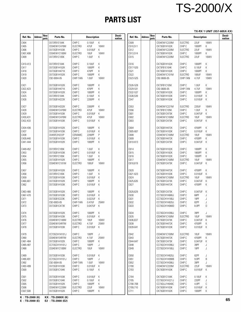
TS-2000/XPARTS LIST
65K : TS-2000 (K) KX : TS-2000X (K)
E : TS-2000 (E) E2 : TS-2000 (E2)
Ref. No. Address Parts No. Description Ref. No. Address Parts No. DescriptionNew Desti-parts nation
New Desti-parts nation
C404 CK73FB1E104K CHIP C 0.10UF KC405 CE04EW1C470M ELECTRO 47UF 16WVC406 CK73GB1H103K CHIP C 0.010UF KC407,408 CE04EW1C100M ELECTRO 10UF 16WVC409 CK73FB1C105K CHIP C 1.0UF K
C410-413 CK73FB1E104K CHIP C 0.10UF KC417 CK73GB1H102K CHIP C 1000PF KC418 CK73GB1H471K CHIP C 470PF KC419 CK73GB1H102K CHIP C 1000PF KC420 C92-0004-05 CHIP-TAN 1.0UF 16WV
C421 CK73GB1H102K CHIP C 1000PF KC422,423 CK73GB1H471K CHIP C 470PF KC424 CK73GB1H102K CHIP C 1000PF KC425 CK73FB1E104K CHIP C 0.10UF KC426 CK73GB1H222K CHIP C 2200PF K
C427 CK73GB1H332K CHIP C 3300PF KC428 CE04EW1C470M ELECTRO 47UF 16WVC429 CK73GB1H103K CHIP C 0.010UF KC430,431 CE04EW1C470M ELECTRO 47UF 16WVC432,433 CK73GB1H103K CHIP C 0.010UF K
C434-436 CK73GB1H102K CHIP C 1000PF KC437 CK73GB1H103K CHIP C 0.010UF KC438 CK45FE2H222P CERAMIC 2200PF PC439,440 CK73GB1H103K CHIP C 0.010UF KC441-444 CK73GB1H102K CHIP C 1000PF K
C449-452 CK73FB1C105K CHIP C 1.0UF KC453 CK73GB1H103K CHIP C 0.010UF KC454 CK73FB1C105K CHIP C 1.0UF KC455 CK73GB1H102K CHIP C 1000PF KC456 CE04EW1C101M ELECTRO 100UF 16WV
C457 CK73GB1H102K CHIP C 1000PF KC458 CK73FB1C105K CHIP C 1.0UF KC459 CK73GB1H103K CHIP C 0.010UF KC460,461 CK73GB1H102K CHIP C 1000PF KC462 CK73GB1H103K CHIP C 0.010UF K
C463-466 CK73GB1H102K CHIP C 1000PF KC467-470 CK73GB1H103K CHIP C 0.010UF KC471 CK73GB1E223K CHIP C 0.022UF KC472 C92-0003-05 CHIP-TAN 0.47UF 25WVC473 CK73GB1C473K CHIP C 0.047UF K
C474 CK73GB1H102K CHIP C 1000PF KC475 CK73GB1H103K CHIP C 0.010UF KC476 CE04EW1C100M ELECTRO 10UF 16WVC477 CE04EW1E4R7M ELECTRO 4.7UF 25WVC478 CK73GB1H103K CHIP C 0.010UF K
C479 CC73GCH1H101J CHIP C 100PF JC480 CE04EW1E4R7M ELECTRO 4.7UF 25WVC481-484 CK73GB1H102K CHIP C 1000PF KC485-487 CC73GCH1H101J CHIP C 100PF JC488 CE04EW1C100M ELECTRO 10UF 16WV
C489 CK73GB1H103K CHIP C 0.010UF KC490,491 CC73GCH1H101J CHIP C 100PF JC492 C92-0004-05 CHIP-TAN 1.0UF 16WVC493-499 CK73GB1H103K CHIP C 0.010UF KC500 CK73GB1C104K CHIP C 0.10UF K
C501 CK73GB1H103K CHIP C 0.010UF KC502 CK73GB1C104K CHIP C 0.10UF KC505 CK73GB1H102K CHIP C 1000PF KC506 CE04EW1C220M ELECTRO 22UF 16WVC507,508 CK73GB1H102K CHIP C 1000PF K
C509 CE04EW1C220M ELECTRO 22UF 16WVC510,511 CK73GB1H102K CHIP C 1000PF KC512 CE04EW1C220M ELECTRO 22UF 16WVC513,514 CK73GB1H102K CHIP C 1000PF KC515 CE04EW1C220M ELECTRO 22UF 16WV
C516 CK73GB1H102K CHIP C 1000PF KC517-520 CK73FB1E104K CHIP C 0.10UF KC521 CK73GB1H102K CHIP C 1000PF KC522 CE04EW1C101M ELECTRO 100UF 16WVC523-525 C92-0606-05 CHIP-TAN 4.7UF 10WV
C526-528 CK73FB1C105K CHIP C 1.0UF KC529-531 C92-0606-05 CHIP-TAN 4.7UF 10WVC532-537 CK73GB1H102K CHIP C 1000PF KC538,539 CK73GB1H103K CHIP C 0.010UF KC547 CK73GB1H103K CHIP C 0.010UF K
C553 CE04EW1C221M ELECTRO 220UF 16WVC556 CK73FB1C105K CHIP C 1.0UF KC601 CK73GB1C473K CHIP C 0.047UF KC602 CE04EW1C100M ELECTRO 10UF 16WVC603 CK73GB1C473K CHIP C 0.047UF K
C604 CK73GB1H472K CHIP C 4700PF KC605-607 CK73GB1H103K CHIP C 0.010UF KC608 CE04EW1C100M ELECTRO 10UF 16WVC609 CK73GB1H472K CHIP C 4700PF KC610-613 CK73GB1C473K CHIP C 0.047UF K
C614 CK73GB1H102K CHIP C 1000PF KC615 CK73GB1H182K CHIP C 1800PF KC616 CK73GB1H102K CHIP C 1000PF KC617 CE04EW1C100M ELECTRO 10UF 16WVC618,619 CK73GB1C473K CHIP C 0.047UF K
C620 CK73GB1H472K CHIP C 4700PF KC621-623 CK73GB1H103K CHIP C 0.010UF KC624 CE04EW1C100M ELECTRO 10UF 16WVC625,626 CK73GB1C473K CHIP C 0.047UF KC627 CK73GB1H472K CHIP C 4700PF K
C628,629 CK73GB1C473K CHIP C 0.047UF KC630 CC73GCH1H680J CHIP C 68PF JC631 CC73GCH1H180J CHIP C 18PF JC632 CC73GCH1H820J CHIP C 82PF JC633 CC73GCH1H080D CHIP C 8.0PF D
C634 CC73GCH1H390J CHIP C 39PF JC635 CE04EW1C100M ELECTRO 10UF 16WVC636,637 CK73GB1C473K CHIP C 0.047UF KC638 CK73GB1H472K CHIP C 4700PF KC639-641 CK73GB1H103K CHIP C 0.010UF K
C642 CE04EW1C100M ELECTRO 10UF 16WVC643 CK73GB1H472K CHIP C 4700PF KC644-647 CK73GB1C473K CHIP C 0.047UF KC648 CC73GCH1H390J CHIP C 39PF JC649 CC73GCH1H180J CHIP C 18PF J
C650 CC73GCH1H820J CHIP C 82PF JC651 CC73GCH1H090B CHIP C 9.0PF BC652 CC73GCH1H390J CHIP C 39PF JC700 CE04EW1C220M ELECTRO 22UF 16WVC703 CK73GB1H103K CHIP C 0.010UF K
C704 CK73GB1C104K CHIP C 0.10UF KC705 CC73GCH1H221J CHIP C 220PF JC706-708 CC73GUJ1H040C CHIP C 4.0PF CC709,710 CK73GB1H103K CHIP C 0.010UF KC711 CK73GB1H102K CHIP C 1000PF K
TX-RX 1 UNIT (X57-605X-XX)

TS-2000/XPARTS LIST
66K : TS-2000 (K) KX : TS-2000X (K)
E : TS-2000 (E) E2 : TS-2000 (E2)
Ref. No. Address Parts No. Description Ref. No. Address Parts No. DescriptionNew Desti-parts nation
New Desti-parts nation
C712-716 CK73GB1H103K CHIP C 0.010UF KC718 CC73GUJ1H040C CHIP C 4.0PF CC719 CK73GB1H103K CHIP C 0.010UF KC720 CC73GCH1H390J CHIP C 39PF JC721,722 CK73GB1C104K CHIP C 0.10UF K
C723 C92-0606-05 CHIP-TAN 4.7UF 10WVC724,725 CK73GB1H103K CHIP C 0.010UF KC726 CK73FB1C105K CHIP C 1.0UF KC727,728 CC73GCH1H101J CHIP C 100PF JC739 CK73GB1H103K CHIP C 0.010UF K
C741 CK73FB1C105K CHIP C 1.0UF KC743 CK73GB1C104K CHIP C 0.10UF KC744 CK73GB1H103K CHIP C 0.010UF KC745,746 CK73GB1C104K CHIP C 0.10UF KC747 CK73FB1C105K CHIP C 1.0UF K
C749 CK73GB1H103K CHIP C 0.010UF KC750 CK73FB1E104K CHIP C 0.10UF KC752 CC73GCH1H560J CHIP C 56PF JC753 CC73GCH1H100D CHIP C 10PF DC754,755 CC73GCH1H271J CHIP C 270PF J
C757 CK73GB1H102K CHIP C 1000PF KC758 CK73GB1E223K CHIP C 0.022UF KC759,760 CK73FB1C105K CHIP C 1.0UF KC761,762 CK73GB1H103K CHIP C 0.010UF KC763 CC73GCH1H030C CHIP C 3.0PF C
C765,766 CK73GB1H103K CHIP C 0.010UF KC767 CC73GCH1H010B CHIP C 1.0PF BC770,771 CK73GB1H102K CHIP C 1000PF KC772 CC73GCH1H470J CHIP C 47PF JC773-776 CK73GB1H102K CHIP C 1000PF K
C777 CC73GCH1H221J CHIP C 220PF JC778 CE04EW1C100M ELECTRO 10UF 16WVC779 CK73GB1C104K CHIP C 0.10UF KC780 CK73GB1H103K CHIP C 0.010UF KC781 CC73GCH1H101J CHIP C 100PF J
C782 C92-0004-05 CHIP-TAN 1.0UF 16WVC783 CK73GB1C104K CHIP C 0.10UF KC784,785 CK73GB1H152K CHIP C 1500PF KC786 CK73FB1C334K CHIP C 0.33UF KC787 CK73FB1E104K CHIP C 0.10UF K
C788,789 CK73FB1C105K CHIP C 1.0UF KC790,791 CK73GB1H103K CHIP C 0.010UF KC792 CK73EB1H104K CHIP C 0.10UF KC800 CK73GB1E223K CHIP C 0.022UF KC801,802 CK73GB1C104K CHIP C 0.10UF K
C803 C92-0038-05 CHIP-ELE 22UF 16WVC804 CK73GB1C104K CHIP C 0.10UF KC806 CK73GB1H102K CHIP C 1000PF KC810,811 CK73GB1C104K CHIP C 0.10UF KC812-816 CK73GB1H102K CHIP C 1000PF K
C818-820 CK73GB1C104K CHIP C 0.10UF KC821,822 CC73GCH1H100D CHIP C 10PF DC823 CK73GB1C104K CHIP C 0.10UF KC824 CK73GB1H103K CHIP C 0.010UF KC826-842 CK73GB1H102K CHIP C 1000PF K
C844 CK73GB1H102K CHIP C 1000PF KC847-850 CK73GB1H102K CHIP C 1000PF KC851 CK73GB1H103K CHIP C 0.010UF KC852-855 CK73GB1H102K CHIP C 1000PF KC858-860 CK73GB1H102K CHIP C 1000PF K
C861 CK73GB1H103K CHIP C 0.010UF KC862-866 CK73GB1H102K CHIP C 1000PF KC867,868 CK73GB1C104K CHIP C 0.10UF KC869 CK73FB1C105K CHIP C 1.0UF KC870,871 CK73GB1C473K CHIP C 0.047UF K
C950,951 CK73GB1H103K CHIP C 0.010UF KC952-955 CK73EF1C105Z CHIP C 1.0UF ZC956-959 CK73GB1H103K CHIP C 0.010UF KC970 CE04EW1A101M ELECTRO 100UF 10WVTC1,2 C05-0344-05 CERAMIC TRIMMER CAP (30P) E,E2
TC3 C05-0369-05 CERAMIC TRIMMER CAP
- E18-0254-05 SOCKET- E23-1176-04 EARTH LUGCN1 E04-0154-05 PIN SOCKETCN2-4 E40-5487-05 PIN ASSYCN5 E04-0154-05 PIN SOCKET
CN6 E40-0211-05 PIN ASSYCN7 E04-0154-05 PIN SOCKETCN9 E40-0211-05 PIN ASSYCN11 E40-3239-05 PIN ASSYCN12 E04-0154-05 PIN SOCKET
CN14 E04-0154-05 PIN SOCKETCN16 E40-3239-05 PIN ASSYCN17,18 E40-3237-05 PIN ASSYCN20 E40-5618-05 FLAT CABLE CONNECTORCN21 E40-5747-05 PIN ASSY SOCKET
CN22,23 E04-0154-05 PIN SOCKETCN24,25 E40-6009-05 FLAT CABLE CONNECTORCN26,27 E40-5978-05 FLAT CABLE CONNECTORCN29 E40-5978-05 FLAT CABLE CONNECTORCN31 E40-3238-05 PIN ASSY
CN32 E40-3239-05 PIN ASSYCN49 E04-0154-05 PIN SOCKETCN800 E40-5978-05 FLAT CABLE CONNECTORCN801 E40-5736-05 FLAT CABLE CONNECTORCN804 E40-3239-05 PIN ASSY
CN805 E40-5978-05 FLAT CABLE CONNECTORCN806 E40-5741-05 FLAT CABLE CONNECTORCN950 E40-3250-05 PIN ASSYCN951 E40-3251-05 PIN ASSYCN952 E40-6074-05 FLAT CABLE CONNECTOR
CN953 E40-6077-05 FLAT CABLE CONNECTORCN956 E40-6079-05 PIN ASSYCN957 E40-6080-05 PIN ASSYCN962 E40-3248-05 PIN ASSYJ1 E13-0166-05 PHONE JACK
J2,3 E11-0414-05 3.5D PHONE JACK (3P)J4 E06-0752-05 DIN SOCKETJ5 E58-0435-05 SUB SOCKET (D)J6 E58-0410-05 MODULAR JACKJ7 E06-0859-05 DIN SOCKET
J8 E56-0408-05 DIN SOCKETJ950 E06-0858-15 RF COAXIAL RECEPTACLE (ROUND)J951 E11-0438-05 PHONE JACK (9P)W1 E37-0884-05 LEAD WIRE WITH CONNECTORW2 E37-0954-05 LEAD WIRE WITH CONNECTOR
- F10-2003-14 SHIELDING CASEF1 F53-0115-05 FUSE
TX-RX 1 UNIT (X57-605X-XX)

TS-2000/XPARTS LIST
67K : TS-2000 (K) KX : TS-2000X (K)
E : TS-2000 (E) E2 : TS-2000 (E2)
Ref. No. Address Parts No. Description Ref. No. Address Parts No. DescriptionNew Desti-parts nation
New Desti-parts nation
- G02-0794-04 FLAT SPRING
CN30 J19-1570-05 HOLDER
CF1 L72-0984-05 CERAMIC FILTERCF2 L72-0985-05 CERAMIC FILTERCF3 L72-0333-05 CERAMIC FILTERCF4 L72-0984-05 CERAMIC FILTERL1 L40-1885-48 SMALL FIXED INDUCTOR (180NH)
L2 L33-0695-05 SMALL FIXED INDUCTORL3,4 L40-6891-14 SMALL FIXED INDUCTORL5,6 L33-0695-05 SMALL FIXED INDUCTORL7 L40-6891-15 SMALL FIXED INDUCTOR E,E2L8 L33-0695-05 SMALL FIXED INDUCTOR
L9 L40-6891-15 SMALL FIXED INDUCTOR E,E2L10 L40-5695-34 SMALL FIXED INDUCTOR (5.6UH)L11 L33-0695-05 SMALL FIXED INDUCTORL12,13 L40-2215-85 SMALL FIXED INDUCTOR (220U)L14 L40-1892-14 SMALL FIXED INDUCTOR
L15 L40-6891-14 SMALL FIXED INDUCTORL16 L40-1892-14 SMALL FIXED INDUCTORL17 L40-1292-14 SMALL FIXED INDUCTORL18 L40-5691-14 SMALL FIXED INDUCTORL19 L40-1292-14 SMALL FIXED INDUCTOR
L20 L40-1092-14 SMALL FIXED INDUCTORL21 L40-3391-14 SMALL FIXED INDUCTORL22 L40-1092-14 SMALL FIXED INDUCTORL23-25 L34-4262-05 COILL26 L40-3382-14 SMALL FIXED INDUCTOR
L27 L40-2792-14 SMALL FIXED INDUCTORL28 L40-3382-14 SMALL FIXED INDUCTORL29 L40-2282-14 SMALL FIXED INDUCTORL30 L40-2292-14 SMALL FIXED INDUCTORL31 L40-2282-14 SMALL FIXED INDUCTOR
L32-34 L34-4289-05 COILL35 L40-2282-14 SMALL FIXED INDUCTORL36 L40-1592-14 SMALL FIXED INDUCTORL37,38 L40-2282-14 SMALL FIXED INDUCTORL39 L40-1292-14 SMALL FIXED INDUCTOR
L40-43 L40-2282-14 SMALL FIXED INDUCTORL44 L34-4333-05 COILL45,46 L34-2026-05 COILL47 L33-0695-05 SMALL FIXED INDUCTORL48 L40-1588-76 SMALL FIXED INDUCTOR (0.15UH)
L49 L40-1088-76 SMALL FIXED INDUCTOR (0.1UH)L50 L40-4705-85 SMALL FIXED INDUCTOR (47U)L51 L19-0324-05 TOROIDAL COILL52 L39-1255-05 TOROIDAL COILL53 L40-1015-85 SMALL FIXED INDUCTOR (100U)
L54 L34-4413-05 COILL55 L33-0695-05 SMALL FIXED INDUCTORL56 L40-2295-85 SMALL FIXED INDUCTOR (2.2U)L57 L33-1394-05 SMALL FIXED INDUCTORL58 L40-1085-34 SMALL FIXED INDUCTOR (100NH)
L59 L33-0695-05 SMALL FIXED INDUCTORL60 L39-1255-05 TOROIDAL COILL61 L40-1015-85 SMALL FIXED INDUCTOR (100U)L62 L34-4394-05 COILL63 L34-4393-05 COIL
L64,65 L34-4394-05 COIL
L66 L34-4393-05 COILL67 L34-4394-05 COILL68 L34-4415-05 COILL69 L34-4207-05 COILL70 L40-1015-85 SMALL FIXED INDUCTOR (100U)
L71 L34-4414-05 COILL72 L40-1085-34 SMALL FIXED INDUCTOR (100NH)L73 L40-2285-34 SMALL FIXED INDUCTOR (220NH)L74-77 L40-1015-85 SMALL FIXED INDUCTOR (100U)L78 L33-0695-05 SMALL FIXED INDUCTOR
L80 L40-4705-85 SMALL FIXED INDUCTOR (47U)L81,82 L34-4401-05 COILL83 L34-4459-05 COILL84-86 L40-2221-33 SMALL FIXED INDUCTORL87 L34-4663-05 COIL
L90 L40-4705-85 SMALL FIXED INDUCTOR (47U)L91 L40-1085-34 SMALL FIXED INDUCTOR (100NH)L92 L33-1394-05 SMALL FIXED INDUCTORL93 L33-0695-05 SMALL FIXED INDUCTORL94 L40-1015-85 SMALL FIXED INDUCTOR (100U)
L95 L19-0324-05 TOROIDAL COILL96 L34-4333-05 COILL97 L39-1255-05 TOROIDAL COILL98-100 L34-4333-05 COILL101 L40-1015-85 SMALL FIXED INDUCTOR (100U)
L102 L34-4222-05 COILL103 L34-4025-05 COILL104 L40-1005-85 SMALL FIXED INDUCTOR (10U)L105 L34-4025-05 COILL106,107 L40-1015-85 SMALL FIXED INDUCTOR (100U)
L108,109 L34-4025-05 COILL110-113 L40-1015-85 SMALL FIXED INDUCTOR (100U)L115,116 L40-1095-85 SMALL FIXED INDUCTOR (1.0U)L117 L40-1021-13 SMALL FIXED INDUCTORL118 L33-1425-05 CHOKE COIL
L119 L33-0695-05 SMALL FIXED INDUCTORL121 L40-1095-85 SMALL FIXED INDUCTOR (1.0U)L122-125 L40-1015-85 SMALL FIXED INDUCTOR (100U)L126 L40-4705-85 SMALL FIXED INDUCTOR (47U)L129-131 L40-1015-85 SMALL FIXED INDUCTOR (100U)
L132-135 L40-1095-85 SMALL FIXED INDUCTOR (1.0U)L601,602 L40-1005-85 SMALL FIXED INDUCTOR (10U)L603,604 L40-1015-85 SMALL FIXED INDUCTOR (100U)L605,606 L40-1005-85 SMALL FIXED INDUCTOR (10U)L607 L40-3395-85 SMALL FIXED INDUCTOR (3.3U)
L608 L40-3995-85 SMALL FIXED INDUCTOR (3.9U)L609,610 L40-1005-85 SMALL FIXED INDUCTOR (10U)L611 L40-2795-85 SMALL FIXED INDUCTOR (2.7U)L612 L40-3395-85 SMALL FIXED INDUCTOR (3.3U)L613 L34-4663-05 COIL
L614 L34-4649-05 COILL615 L40-1015-85 SMALL FIXED INDUCTOR (100U)L616,617 L40-3301-37 SMALL FIXED INDUCTOR (33.00UH)L618 L40-1005-85 SMALL FIXED INDUCTOR (10U)L700 L40-1885-34 SMALL FIXED INDUCTOR (180NH)
L701 L33-0695-05 SMALL FIXED INDUCTORL702 L40-2295-85 SMALL FIXED INDUCTOR (2.2U)L703 L33-1394-05 SMALL FIXED INDUCTORL704 L40-1085-34 SMALL FIXED INDUCTOR (100NH)L705 L33-0695-05 SMALL FIXED INDUCTOR
TX-RX 1 UNIT (X57-605X-XX)

TS-2000/XPARTS LIST
68K : TS-2000 (K) KX : TS-2000X (K)
E : TS-2000 (E) E2 : TS-2000 (E2)
Ref. No. Address Parts No. Description Ref. No. Address Parts No. DescriptionNew Desti-parts nation
New Desti-parts nation
L706 L33-1394-05 SMALL FIXED INDUCTORL707 L40-1081-36 SMALL FIXED INDUCTOR (100NH)L709 L40-3395-34 SMALL FIXED INDUCTOR (3.3UH)L710-713 L40-3391-37 SMALL FIXED INDUCTOR (3.300UH)L714,715 L40-1005-85 SMALL FIXED INDUCTOR (10U)
L716 L40-4705-34 SMALL FIXED INDUCTOR (47UH)L717 L92-0131-05 FERRITE CHIPL718 L40-1015-85 SMALL FIXED INDUCTOR (100U)L800,801 L40-1095-48 SMALL FIXED INDUCTOR (1UH)X1 L77-1827-05 CRYSTAL RESONATOR (10.595M)
X800 L77-1680-05 CRYSTAL RESONATOR (11.0592MHZ)XF1 L71-0562-05 MCF (69.085M)XF2 L71-0561-05 MCF (75.925M)XF5 L71-0433-15 MCF (10.695MHZ)XF6 L71-0569-05 CRYSTAL FILTER (10.695M/2.7K)
XF9 L71-0570-05 CRYSTAL FILTER (10.595M/6K)
CP1-3 RK75GB1J103J CHIP-COM 10K J 1/16WCP6-9 RK75GB1J103J CHIP-COM 10K J 1/16WCP10,11 RK75GB1J101J CHIP-COM 100 J 1/16WCP801-804 RK75GB1J473J CHIP-COM 47K J 1/16WCP805-808 RK75GB1J103J CHIP-COM 10K J 1/16W
CP809,810 RK75GB1J473J CHIP-COM 47K J 1/16WR1 RK73EB2B560J CHIP R 56 J 1/8WR2 RK73EB2B471J CHIP R 470 J 1/8WR3 RK73EB2B181J CHIP R 180 J 1/8WR4 RK73GB1J222J CHIP R 2.2K J 1/16W
R5 RK73GB1J101J CHIP R 100 J 1/16WR6,7 RK73FB2A101J CHIP R 100 J 1/10WR8 RK73GB1J472J CHIP R 4.7K J 1/16WR9 RK73GB1J471J CHIP R 470 J 1/16WR10 RK73GB1J560J CHIP R 56 J 1/16W
R11-13 RK73FB2A560J CHIP R 56 J 1/10WR14 RK73GB1J330J CHIP R 33 J 1/16WR15,16 RK73FB2A560J CHIP R 56 J 1/10WR17 RK73GB1J330J CHIP R 33 J 1/16WR18,19 RK73FB2A560J CHIP R 56 J 1/10W
R20 RK73GB1J330J CHIP R 33 J 1/16WR21,22 RK73FB2A560J CHIP R 56 J 1/10WR23 RK73GB1J330J CHIP R 33 J 1/16WR24,25 RK73FB2A560J CHIP R 56 J 1/10WR26 RK73GB1J330J CHIP R 33 J 1/16W
R27,28 RK73FB2A560J CHIP R 56 J 1/10WR29 RK73GB1J330J CHIP R 33 J 1/16WR30,31 RK73FB2A560J CHIP R 56 J 1/10WR32 RK73GB1J330J CHIP R 33 J 1/16WR33,34 RK73FB2A560J CHIP R 56 J 1/10W
R35 RK73GB1J330J CHIP R 33 J 1/16WR36,37 RK73FB2A560J CHIP R 56 J 1/10WR38 RK73GB1J330J CHIP R 33 J 1/16WR39,40 RK73FB2A560J CHIP R 56 J 1/10WR41 RK73GB1J330J CHIP R 33 J 1/16W
R42 RK73FB2A560J CHIP R 56 J 1/10WR43 RK73GB1J330J CHIP R 33 J 1/16WR44,45 RK73FB2A560J CHIP R 56 J 1/10WR46 RK73GB1J151J CHIP R 150 J 1/16WR47 RK73GB1J562J CHIP R 5.6K J 1/16W
R48 RK73GB1J471J CHIP R 470 J 1/16WR49 RK73GB1J102J CHIP R 1.0K J 1/16WR50,51 RK73GB1J681J CHIP R 680 J 1/16W
R52 R92-1252-05 CHIP R 0 OHMR53,54 RK73GB1J100J CHIP R 10 J 1/16WR55 RK73GB1J271J CHIP R 270 J 1/16WR56,57 RK73GB1J100J CHIP R 10 J 1/16WR58 RK73GB1J682J CHIP R 6.8K J 1/16W
R59 RK73FB2A100J CHIP R 10 J 1/10WR60 RK73GB1J471J CHIP R 470 J 1/16WR61 RK73GB1J151J CHIP R 150 J 1/16WR62 RK73GB1J331J CHIP R 330 J 1/16WR63 RK73GB1J681J CHIP R 680 J 1/16W
R64 RK73GB1J103J CHIP R 10K J 1/16WR65 RK73FB2A100J CHIP R 10 J 1/10WR68 RK73GB1J331J CHIP R 330 J 1/16WR69 RK73GB1J180J CHIP R 18 J 1/16WR70 RK73GB1J331J CHIP R 330 J 1/16W
R71 RK73GB1J151J CHIP R 150 J 1/16WR72 R92-1252-05 CHIP R 0 OHMR73 RK73GB1J102J CHIP R 1.0K J 1/16WR74 RK73GB1J100J CHIP R 10 J 1/16WR75 RK73GB1J680J CHIP R 68 J 1/16W
R76 RK73GB1J180J CHIP R 18 J 1/16WR77 RK73GB1J182J CHIP R 1.8K J 1/16WR78 RK73GB1J102J CHIP R 1.0K J 1/16WR79 RK73GB1J471J CHIP R 470 J 1/16WR80 RK73GB1J103J CHIP R 10K J 1/16W
R81 RK73GB1J560J CHIP R 56 J 1/16WR82 RK73GB1J103J CHIP R 10K J 1/16WR83-86 RK73GB1J471J CHIP R 470 J 1/16WR87 RK73GB1J222J CHIP R 2.2K J 1/16WR88,89 RK73GB1J471J CHIP R 470 J 1/16W
R90 RK73GB1J273J CHIP R 27K J 1/16WR91 RK73GB1J471J CHIP R 470 J 1/16WR92 RK73GB1J823J CHIP R 82K J 1/16WR93 RK73GB1J100J CHIP R 10 J 1/16WR94 RK73GB1J101J CHIP R 100 J 1/16W
R95 RK73GB1J102J CHIP R 1.0K J 1/16WR96 R92-1252-05 CHIP R 0 OHMR97 RK73GB1J682J CHIP R 6.8K J 1/16WR98 R92-1252-05 CHIP R 0 OHMR99,100 RK73GB1J222J CHIP R 2.2K J 1/16W
R101 RK73GB1J102J CHIP R 1.0K J 1/16WR102 RK73FB2A100J CHIP R 10 J 1/10WR103 RK73GB1J682J CHIP R 6.8K J 1/16WR104 RK73GB1J221J CHIP R 220 J 1/16WR105 RK73GB1J821J CHIP R 820 J 1/16W
R106,107 RK73GB1J102J CHIP R 1.0K J 1/16WR108 RK73GB1J101J CHIP R 100 J 1/16WR110 RK73GB1J104J CHIP R 100K J 1/16WR111 RK73GB1J222J CHIP R 2.2K J 1/16WR113 RK73GB1J471J CHIP R 470 J 1/16W
R114 RK73GB1J222J CHIP R 2.2K J 1/16WR115 RK73GB1J101J CHIP R 100 J 1/16WR119 RK73GB1J104J CHIP R 100K J 1/16WR121 RK73GB1J103J CHIP R 10K J 1/16WR122 RK73GB1J151J CHIP R 150 J 1/16W
R123 RK73GB1J471J CHIP R 470 J 1/16WR124 RK73GB1J122J CHIP R 1.2K J 1/16WR126 R92-1252-05 CHIP R 0 OHMR127 RK73GB1J122J CHIP R 1.2K J 1/16WR128 RK73GB1J152J CHIP R 1.5K J 1/16W
TX-RX 1 UNIT (X57-605X-XX)

TS-2000/XPARTS LIST
69K : TS-2000 (K) KX : TS-2000X (K)
E : TS-2000 (E) E2 : TS-2000 (E2)
Ref. No. Address Parts No. Description Ref. No. Address Parts No. DescriptionNew Desti-parts nation
New Desti-parts nation
R131 RK73GB1J101J CHIP R 100 J 1/16WR132 R92-1252-05 CHIP R 0 OHMR133 RK73GB1J101J CHIP R 100 J 1/16WR135 R92-1252-05 CHIP R 0 OHMR137 RK73GB1J681J CHIP R 680 J 1/16W
R138 RK73GB1J152J CHIP R 1.5K J 1/16WR139 RK73GB1J101J CHIP R 100 J 1/16WR141 RK73GB1J681J CHIP R 680 J 1/16WR142 R92-1252-05 CHIP R 0 OHMR143 RK73GB1J681J CHIP R 680 J 1/16W
R144,145 RK73GB1J152J CHIP R 1.5K J 1/16WR146 RK73GB1J101J CHIP R 100 J 1/16WR147 RK73GB1J681J CHIP R 680 J 1/16WR148 RK73GB1J821J CHIP R 820 J 1/16WR149 RK73GB1J122J CHIP R 1.2K J 1/16W
R150 RK73GB1J681J CHIP R 680 J 1/16WR151 RK73GB1J221J CHIP R 220 J 1/16WR152 RK73GB1J102J CHIP R 1.0K J 1/16WR153 RK73GB1J223J CHIP R 22K J 1/16WR154 R92-1252-05 CHIP R 0 OHM
R155 RK73GB1J223J CHIP R 22K J 1/16WR157 RK73GB1J683J CHIP R 68K J 1/16WR158,159 RK73GB1J103J CHIP R 10K J 1/16WR160 RK73GB1J102J CHIP R 1.0K J 1/16WR161 RK73GB1J152J CHIP R 1.5K J 1/16W
R162 RK73GB1J223J CHIP R 22K J 1/16WR163 RK73GB1J221J CHIP R 220 J 1/16WR165 RK73GB1J102J CHIP R 1.0K J 1/16WR166 RK73GB1J563J CHIP R 56K J 1/16WR167 RK73GB1J101J CHIP R 100 J 1/16W
R168 RK73GB1J681J CHIP R 680 J 1/16WR169 RK73GB1J682J CHIP R 6.8K J 1/16WR172 RK73GB1J104J CHIP R 100K J 1/16WR173 RK73GB1J223J CHIP R 22K J 1/16WR174 RK73GB1J471J CHIP R 470 J 1/16W
R175 RK73GB1J223J CHIP R 22K J 1/16WR176 RK73GB1J822J CHIP R 8.2K J 1/16WR177 RK73GB1J471J CHIP R 470 J 1/16WR178 RK73GB1J560J CHIP R 56 J 1/16WR179 RK73GB1J221J CHIP R 220 J 1/16W
R180 RK73GB1J274J CHIP R 270K J 1/16WR181 RK73GB1J152J CHIP R 1.5K J 1/16WR182 RK73GB1J273J CHIP R 27K J 1/16WR183 RK73GB1J152J CHIP R 1.5K J 1/16WR184 RK73GB1J101J CHIP R 100 J 1/16W
R185 RK73GB1J332J CHIP R 3.3K J 1/16WR187 RK73GB1J101J CHIP R 100 J 1/16WR188 RK73GB1J152J CHIP R 1.5K J 1/16WR190 RK73GB1J332J CHIP R 3.3K J 1/16WR191 RK73GB1J101J CHIP R 100 J 1/16W
R192 RK73GB1J332J CHIP R 3.3K J 1/16WR194 RK73GB1J101J CHIP R 100 J 1/16WR196 RK73GB1J332J CHIP R 3.3K J 1/16WR197 RK73GB1J101J CHIP R 100 J 1/16WR198 RK73GB1J332J CHIP R 3.3K J 1/16W
R200 RK73GB1J101J CHIP R 100 J 1/16WR201 RK73GB1J103J CHIP R 10K J 1/16WR202 RK73GB1J332J CHIP R 3.3K J 1/16WR203,204 RK73GB1J154J CHIP R 150K J 1/16WR205 RK73GB1J563J CHIP R 56K J 1/16W
R206 RK73GB1J682J CHIP R 6.8K J 1/16WR209 RK73GB1J470J CHIP R 47 J 1/16WR210 RK73GB1J102J CHIP R 1.0K J 1/16WR211,212 RK73GB1J103J CHIP R 10K J 1/16WR213 RK73GB1J223J CHIP R 22K J 1/16W
R214 RK73GB1J122J CHIP R 1.2K J 1/16WR215,216 RK73GB1J332J CHIP R 3.3K J 1/16WR217 RK73GB1J104J CHIP R 100K J 1/16WR219 RK73GB1J471J CHIP R 470 J 1/16WR220 RK73GB1J223J CHIP R 22K J 1/16W
R221 RK73GB1J101J CHIP R 100 J 1/16WR222 RK73GB1J222J CHIP R 2.2K J 1/16WR223 RK73GB1J221J CHIP R 220 J 1/16WR224 RK73GB1J682J CHIP R 6.8K J 1/16WR225 RK73GB1J331J CHIP R 330 J 1/16W
R226 RK73GB1J152J CHIP R 1.5K J 1/16WR227 R92-1252-05 CHIP R 0 OHMR228 RK73GB1J331J CHIP R 330 J 1/16WR229 RK73GB1J101J CHIP R 100 J 1/16WR230-232 RK73GB1J102J CHIP R 1.0K J 1/16W
R233 RK73GB1J154J CHIP R 150K J 1/16WR234 RK73GB1J101J CHIP R 100 J 1/16WR235 RK73GB1J124J CHIP R 120K J 1/16WR236 RK73GB1J472J CHIP R 4.7K J 1/16WR237 RK73GB1J471J CHIP R 470 J 1/16W
R240 RK73GB1J100J CHIP R 10 J 1/16WR241 RK73GB1J223J CHIP R 22K J 1/16WR242,243 RK73GB1J472J CHIP R 4.7K J 1/16WR244 RK73GB1J331J CHIP R 330 J 1/16WR245 RK73GB1J180J CHIP R 18 J 1/16W
R246 RK73GB1J331J CHIP R 330 J 1/16WR247 RK73FB2A100J CHIP R 10 J 1/10WR248 RK73GB1J221J CHIP R 220 J 1/16WR249 RK73GB1J681J CHIP R 680 J 1/16WR250 RK73GB1J103J CHIP R 10K J 1/16W
R252 RK73GB1J151J CHIP R 150 J 1/16WR253 RK73GB1J101J CHIP R 100 J 1/16WR254 RK73GB1J151J CHIP R 150 J 1/16WR255 R92-1252-05 CHIP R 0 OHMR256 RK73GB1J681J CHIP R 680 J 1/16W
R257,258 R92-1252-05 CHIP R 0 OHMR259,260 RK73GB1J100J CHIP R 10 J 1/16WR261,262 RK73GB1J330J CHIP R 33 J 1/16WR263 RK73GB1J473J CHIP R 47K J 1/16WR264 RK73GB1J104J CHIP R 100K J 1/16W
R265 RK73GB1J103J CHIP R 10K J 1/16WR266,267 RK73GB1J330J CHIP R 33 J 1/16WR268 RK73GB1J273J CHIP R 27K J 1/16WR269 RK73GB1J102J CHIP R 1.0K J 1/16WR270 RK73GB1J473J CHIP R 47K J 1/16W
R272-274 RK73GB1J104J CHIP R 100K J 1/16WR275,276 RK73GB1J101J CHIP R 100 J 1/16WR277,278 RK73GB1J331J CHIP R 330 J 1/16WR279 RK73GB1J472J CHIP R 4.7K J 1/16WR280,281 RK73GB1J330J CHIP R 33 J 1/16W
R282,283 RK73GB1J680J CHIP R 68 J 1/16WR284 RK73GB1J103J CHIP R 10K J 1/16WR285 RK73GB1J472J CHIP R 4.7K J 1/16WR286 R92-1252-05 CHIP R 0 OHMR287,288 RK73GB1J102J CHIP R 1.0K J 1/16W
TX-RX 1 UNIT (X57-605X-XX)

TS-2000/XPARTS LIST
70K : TS-2000 (K) KX : TS-2000X (K)
E : TS-2000 (E) E2 : TS-2000 (E2)
Ref. No. Address Parts No. Description Ref. No. Address Parts No. DescriptionNew Desti-parts nation
New Desti-parts nation
R289 RK73GB1J471J CHIP R 470 J 1/16WR290 RK73GB1J151J CHIP R 150 J 1/16WR291 RK73GB1J124J CHIP R 120K J 1/16WR292 RK73GB1J330J CHIP R 33 J 1/16WR293 RK73GB1J681J CHIP R 680 J 1/16W
R294 RK73GB1J103J CHIP R 10K J 1/16WR295 RK73GB1J682J CHIP R 6.8K J 1/16WR296 RK73GB1J103J CHIP R 10K J 1/16WR297,298 RK73GB1J122J CHIP R 1.2K J 1/16WR299 RK73GB1J681J CHIP R 680 J 1/16W
R300 RK73GB1J223J CHIP R 22K J 1/16WR301 RK73GB1J561J CHIP R 560 J 1/16WR302 RK73GB1J682J CHIP R 6.8K J 1/16WR303 RK73GB1J102J CHIP R 1.0K J 1/16WR304 RK73GB1J223J CHIP R 22K J 1/16W
R305 RK73GB1J151J CHIP R 150 J 1/16WR306 RK73GB1J103J CHIP R 10K J 1/16WR307 RK73GB1J681J CHIP R 680 J 1/16WR308 RK73GB1J472J CHIP R 4.7K J 1/16WR309 RK73GB1J101J CHIP R 100 J 1/16W
R311 RK73GB1J223J CHIP R 22K J 1/16WR313 RK73GB1J681J CHIP R 680 J 1/16WR315 RK73GB1J222J CHIP R 2.2K J 1/16WR316 RK73GB1J682J CHIP R 6.8K J 1/16WR317 RK73GB1J102J CHIP R 1.0K J 1/16W
R319 RK73GB1J562J CHIP R 5.6K J 1/16WR320 RK73GB1J473J CHIP R 47K J 1/16WR321 RK73GB1J223J CHIP R 22K J 1/16WR322-324 RK73GB1J473J CHIP R 47K J 1/16WR325 RK73GB1J222J CHIP R 2.2K J 1/16W
R326 RK73GB1J330J CHIP R 33 J 1/16WR327 RK73GB1J102J CHIP R 1.0K J 1/16WR328 RK73GB1J122J CHIP R 1.2K J 1/16WR329 RK73GB1J182J CHIP R 1.8K J 1/16WR330 RK73GB1J681J CHIP R 680 J 1/16W
R331 RK73GB1J122J CHIP R 1.2K J 1/16WR332 RK73GB1J331J CHIP R 330 J 1/16WR333 RK73GB1J471J CHIP R 470 J 1/16WR334 RK73GB1J101J CHIP R 100 J 1/16WR335 RK73GB1J102J CHIP R 1.0K J 1/16W
R336 RK73GB1J222J CHIP R 2.2K J 1/16WR337 RK73GB1J224J CHIP R 220K J 1/16WR338 RK73GB1J331J CHIP R 330 J 1/16WR339 RK73GB1J101J CHIP R 100 J 1/16WR340 RK73GB1J274J CHIP R 270K J 1/16W
R341 RD14BB2C103J RD 10K J 1/6WR342 RK73GB1J103J CHIP R 10K J 1/16WR343 RK73GB1J681J CHIP R 680 J 1/16WR344 RK73GB1J223J CHIP R 22K J 1/16WR345 RK73GB1J332J CHIP R 3.3K J 1/16W
R346 RK73GB1J681J CHIP R 680 J 1/16WR347 RK73GB1J471J CHIP R 470 J 1/16WR348 RK73GB1J332J CHIP R 3.3K J 1/16WR349 RK73GB1J101J CHIP R 100 J 1/16WR350 RK73GB1J102J CHIP R 1.0K J 1/16W
R351 RK73GB1J223J CHIP R 22K J 1/16WR352 RK73GB1J683J CHIP R 68K J 1/16WR355 RK73GB1J102J CHIP R 1.0K J 1/16WR356 RK73GB1J474J CHIP R 470K J 1/16WR359 RK73GB1J104J CHIP R 100K J 1/16W
R361 RK73GB1J103J CHIP R 10K J 1/16WR364 RK73GB1J473J CHIP R 47K J 1/16WR365 RK73GB1J273J CHIP R 27K J 1/16WR366 RK73GB1J271J CHIP R 270 J 1/16WR367,368 RK73GB1J4R7J CHIP R 4.7 J 1/16W
R369 RK73GB1J271J CHIP R 270 J 1/16WR370 RK73GB1J273J CHIP R 27K J 1/16WR371 RK73GB1J102J CHIP R 1.0K J 1/16WR372 RK73GB1J473J CHIP R 47K J 1/16WR373,374 RK73GB1J472J CHIP R 4.7K J 1/16W
R375 RK73GB1J102J CHIP R 1.0K J 1/16WR376 RK73GB1J331J CHIP R 330 J 1/16WR377 RK73GB1J104J CHIP R 100K J 1/16WR378 RK73GB1J331J CHIP R 330 J 1/16WR379 RK73GB1J272J CHIP R 2.7K J 1/16W
R380,381 RK73GB1J223J CHIP R 22K J 1/16WR382 RK73GB1J471J CHIP R 470 J 1/16WR383 RK73GB1J223J CHIP R 22K J 1/16WR384,385 RK73GB1J101J CHIP R 100 J 1/16WR386 RK73GB1J103J CHIP R 10K J 1/16W
R387 RK73GB1J472J CHIP R 4.7K J 1/16WR391 RK73GB1J103J CHIP R 10K J 1/16WR392 RK73GB1J100J CHIP R 10 J 1/16WR397 RK73GB1J104J CHIP R 100K J 1/16WR398,399 R92-1252-05 CHIP R 0 OHM
R400 RK73GB1J103J CHIP R 10K J 1/16WR401-404 RK73GB1J101J CHIP R 100 J 1/16WR405-408 RK73GB1J2R2J CHIP R 2.2 J 1/16WR409,410 RK73GB1J104J CHIP R 100K J 1/16WR411 RK73GB1J822J CHIP R 8.2K J 1/16W
R412 RK73GB1J222J CHIP R 2.2K J 1/16WR413 RK73GB1J103J CHIP R 10K J 1/16WR414 RK73GB1J153J CHIP R 15K J 1/16WR415,416 RK73GB1J102J CHIP R 1.0K J 1/16WR417 RK73GB1J222J CHIP R 2.2K J 1/16W
R418,419 RK73GB1J331J CHIP R 330 J 1/16WR420 RK73GB1J102J CHIP R 1.0K J 1/16WR421 RK73GB1J101J CHIP R 100 J 1/16WR422 RK73GB1J104J CHIP R 100K J 1/16WR423 RK73GB1J153J CHIP R 15K J 1/16W
R424 RK73GB1J222J CHIP R 2.2K J 1/16WR425 RK73GB1J332J CHIP R 3.3K J 1/16WR426 RK73GB1J104J CHIP R 100K J 1/16WR427 RK73GB1J332J CHIP R 3.3K J 1/16WR428 RK73GB1J822J CHIP R 8.2K J 1/16W
R429 RK73GB1J100J CHIP R 10 J 1/16WR430 R92-1252-05 CHIP R 0 OHMR431 RK73GB1J104J CHIP R 100K J 1/16WR432 R92-1252-05 CHIP R 0 OHMR433-435 RK73GB1J104J CHIP R 100K J 1/16W
R438,439 RK73GB1J104J CHIP R 100K J 1/16WR440 RK73GB1J224J CHIP R 220K J 1/16WR442 RK73GB1J273J CHIP R 27K J 1/16WR443 R92-1252-05 CHIP R 0 OHMR444 RK73GB1J103J CHIP R 10K J 1/16W
R445 RK73GB1J102J CHIP R 1.0K J 1/16WR446-448 RK73GB1J104J CHIP R 100K J 1/16WR449 RK73GB1J221J CHIP R 220 J 1/16WR450 RK73GB1J102J CHIP R 1.0K J 1/16WR451 RK73GB1J272J CHIP R 2.7K J 1/16W
TX-RX 1 UNIT (X57-605X-XX)
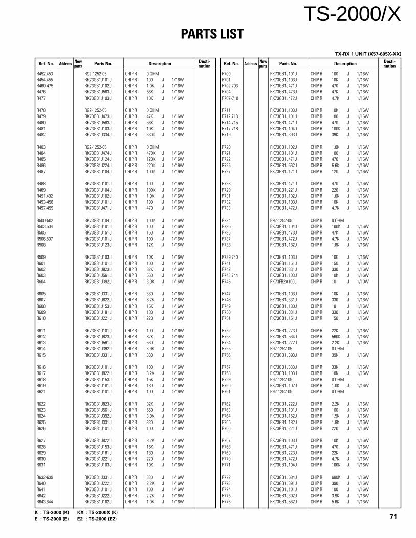
TS-2000/XPARTS LIST
71K : TS-2000 (K) KX : TS-2000X (K)
E : TS-2000 (E) E2 : TS-2000 (E2)
Ref. No. Address Parts No. Description Ref. No. Address Parts No. DescriptionNew Desti-parts nation
New Desti-parts nation
R452,453 R92-1252-05 CHIP R 0 OHMR454,455 RK73GB1J101J CHIP R 100 J 1/16WR460-475 RK73GB1J102J CHIP R 1.0K J 1/16WR476 RK73GB1J563J CHIP R 56K J 1/16WR477 RK73GB1J103J CHIP R 10K J 1/16W
R478 R92-1252-05 CHIP R 0 OHMR479 RK73GB1J473J CHIP R 47K J 1/16WR480 RK73GB1J563J CHIP R 56K J 1/16WR481 RK73GB1J103J CHIP R 10K J 1/16WR482 RK73GB1J334J CHIP R 330K J 1/16W
R483 R92-1252-05 CHIP R 0 OHMR484 RK73GB1J474J CHIP R 470K J 1/16WR485 RK73GB1J124J CHIP R 120K J 1/16WR486 RK73GB1J224J CHIP R 220K J 1/16WR487 RK73GB1J104J CHIP R 100K J 1/16W
R488 RK73GB1J101J CHIP R 100 J 1/16WR489 RK73GB1J104J CHIP R 100K J 1/16WR491,492 RK73GB1J102J CHIP R 1.0K J 1/16WR493-496 RK73GB1J101J CHIP R 100 J 1/16WR497-499 RK73GB1J471J CHIP R 470 J 1/16W
R500-502 RK73GB1J104J CHIP R 100K J 1/16WR503,504 RK73GB1J101J CHIP R 100 J 1/16WR505 RK73GB1J151J CHIP R 150 J 1/16WR506,507 RK73GB1J101J CHIP R 100 J 1/16WR508 RK73GB1J123J CHIP R 12K J 1/16W
R509 RK73GB1J103J CHIP R 10K J 1/16WR601 RK73GB1J101J CHIP R 100 J 1/16WR602 RK73GB1J823J CHIP R 82K J 1/16WR603 RK73GB1J561J CHIP R 560 J 1/16WR604 RK73GB1J392J CHIP R 3.9K J 1/16W
R605 RK73GB1J331J CHIP R 330 J 1/16WR607 RK73GB1J822J CHIP R 8.2K J 1/16WR608 RK73GB1J153J CHIP R 15K J 1/16WR609 RK73GB1J181J CHIP R 180 J 1/16WR610 RK73GB1J221J CHIP R 220 J 1/16W
R611 RK73GB1J101J CHIP R 100 J 1/16WR612 RK73GB1J823J CHIP R 82K J 1/16WR613 RK73GB1J561J CHIP R 560 J 1/16WR614 RK73GB1J392J CHIP R 3.9K J 1/16WR615 RK73GB1J331J CHIP R 330 J 1/16W
R616 RK73GB1J101J CHIP R 100 J 1/16WR617 RK73GB1J822J CHIP R 8.2K J 1/16WR618 RK73GB1J153J CHIP R 15K J 1/16WR619 RK73GB1J181J CHIP R 180 J 1/16WR621 RK73GB1J101J CHIP R 100 J 1/16W
R622 RK73GB1J823J CHIP R 82K J 1/16WR623 RK73GB1J561J CHIP R 560 J 1/16WR624 RK73GB1J392J CHIP R 3.9K J 1/16WR625 RK73GB1J331J CHIP R 330 J 1/16WR626 RK73GB1J101J CHIP R 100 J 1/16W
R627 RK73GB1J822J CHIP R 8.2K J 1/16WR628 RK73GB1J153J CHIP R 15K J 1/16WR629 RK73GB1J181J CHIP R 180 J 1/16WR630 RK73GB1J221J CHIP R 220 J 1/16WR631 RK73GB1J103J CHIP R 10K J 1/16W
R632-639 RK73GB1J331J CHIP R 330 J 1/16WR640 RK73GB1J222J CHIP R 2.2K J 1/16WR641 RK73GB1J101J CHIP R 100 J 1/16WR642 RK73GB1J222J CHIP R 2.2K J 1/16WR643,644 RK73GB1J102J CHIP R 1.0K J 1/16W
R700 RK73GB1J101J CHIP R 100 J 1/16WR701 RK73GB1J103J CHIP R 10K J 1/16WR702,703 RK73GB1J471J CHIP R 470 J 1/16WR704 RK73GB1J473J CHIP R 47K J 1/16WR707-710 RK73GB1J472J CHIP R 4.7K J 1/16W
R711 RK73GB1J103J CHIP R 10K J 1/16WR712,713 RK73GB1J101J CHIP R 100 J 1/16WR714,715 RK73GB1J471J CHIP R 470 J 1/16WR717,718 RK73GB1J104J CHIP R 100K J 1/16WR719 RK73GB1J393J CHIP R 39K J 1/16W
R720 RK73GB1J102J CHIP R 1.0K J 1/16WR721 RK73GB1J101J CHIP R 100 J 1/16WR722 RK73GB1J471J CHIP R 470 J 1/16WR725 RK73GB1J562J CHIP R 5.6K J 1/16WR727 RK73GB1J121J CHIP R 120 J 1/16W
R728 RK73GB1J471J CHIP R 470 J 1/16WR729 RK73GB1J221J CHIP R 220 J 1/16WR731 RK73GB1J102J CHIP R 1.0K J 1/16WR732 RK73GB1J103J CHIP R 10K J 1/16WR733 RK73GB1J472J CHIP R 4.7K J 1/16W
R734 R92-1252-05 CHIP R 0 OHMR735 RK73GB1J104J CHIP R 100K J 1/16WR736 RK73GB1J473J CHIP R 47K J 1/16WR737 RK73GB1J472J CHIP R 4.7K J 1/16WR738 RK73GB1J182J CHIP R 1.8K J 1/16W
R739,740 RK73GB1J103J CHIP R 10K J 1/16WR741 RK73GB1J151J CHIP R 150 J 1/16WR742 RK73GB1J331J CHIP R 330 J 1/16WR743,744 RK73GB1J103J CHIP R 10K J 1/16WR745 RK73FB2A100J CHIP R 10 J 1/10W
R747 RK73GB1J103J CHIP R 10K J 1/16WR748 RK73GB1J331J CHIP R 330 J 1/16WR749 RK73GB1J180J CHIP R 18 J 1/16WR750 RK73GB1J331J CHIP R 330 J 1/16WR751 RK73GB1J151J CHIP R 150 J 1/16W
R752 RK73GB1J223J CHIP R 22K J 1/16WR753 RK73GB1J564J CHIP R 560K J 1/16WR754 RK73GB1J222J CHIP R 2.2K J 1/16WR755 R92-1252-05 CHIP R 0 OHMR756 RK73GB1J393J CHIP R 39K J 1/16W
R757 RK73GB1J333J CHIP R 33K J 1/16WR758 RK73GB1J103J CHIP R 10K J 1/16WR759 R92-1252-05 CHIP R 0 OHMR760 RK73GB1J102J CHIP R 1.0K J 1/16WR761 R92-1252-05 CHIP R 0 OHM
R762 RK73GB1J222J CHIP R 2.2K J 1/16WR763 RK73GB1J101J CHIP R 100 J 1/16WR764 RK73GB1J152J CHIP R 1.5K J 1/16WR765 RK73GB1J182J CHIP R 1.8K J 1/16WR766 RK73GB1J221J CHIP R 220 J 1/16W
R767 RK73GB1J103J CHIP R 10K J 1/16WR768 RK73GB1J471J CHIP R 470 J 1/16WR769 RK73GB1J223J CHIP R 22K J 1/16WR770 RK73GB1J472J CHIP R 4.7K J 1/16WR771 RK73GB1J104J CHIP R 100K J 1/16W
R772 RK73GB1J684J CHIP R 680K J 1/16WR773 RK73GB1J391J CHIP R 390 J 1/16WR774 RK73GB1J101J CHIP R 100 J 1/16WR775 RK73GB1J392J CHIP R 3.9K J 1/16WR776 RK73GB1J562J CHIP R 5.6K J 1/16W
TX-RX 1 UNIT (X57-605X-XX)

TS-2000/XPARTS LIST
72K : TS-2000 (K) KX : TS-2000X (K)
E : TS-2000 (E) E2 : TS-2000 (E2)
Ref. No. Address Parts No. Description Ref. No. Address Parts No. DescriptionNew Desti-parts nation
New Desti-parts nation
R777 RK73GB1J473J CHIP R 47K J 1/16WR778 RK73GB1J184J CHIP R 180K J 1/16WR779 RK73GB1J102J CHIP R 1.0K J 1/16WR780 RK73GB1J101J CHIP R 100 J 1/16WR781 RK73GB1J152J CHIP R 1.5K J 1/16W
R782 RK73GB1J124J CHIP R 120K J 1/16WR783 RK73GB1J471J CHIP R 470 J 1/16WR785,786 RK73GB1J2R2J CHIP R 2.2 J 1/16WR787 RK73FB2A473J CHIP R 47K J 1/10WR800 RK73FB2A681J CHIP R 680 J 1/10W
R801 RK73FB2A222J CHIP R 2.2K J 1/10WR802 RK73FB2A681J CHIP R 680 J 1/10WR803 RK73FB2A102J CHIP R 1.0K J 1/10WR804 RK73FB2A681J CHIP R 680 J 1/10WR805 RK73FB2A682J CHIP R 6.8K J 1/10W
R806 RK73FB2A681J CHIP R 680 J 1/10WR807 RK73FB2A102J CHIP R 1.0K J 1/10WR808 RK73FB2A681J CHIP R 680 J 1/10WR809 RK73FB2A222J CHIP R 2.2K J 1/10WR818-822 RK73GB1J101J CHIP R 100 J 1/16W
R823 R92-1252-05 CHIP R 0 OHMR824 R92-0670-05 CHIP R 0 OHMR841 RK73GB1J473J CHIP R 47K J 1/16WR842 R92-1252-05 CHIP R 0 OHMR846-853 RK73GB1J101J CHIP R 100 J 1/16W
R855-862 RK73GB1J101J CHIP R 100 J 1/16WR864 RK73GB1J101J CHIP R 100 J 1/16WR867-871 RK73FB2A680J CHIP R 68 J 1/10WR872 RK73GB1J103J CHIP R 10K J 1/16WR873 RK73GB1J101J CHIP R 100 J 1/16W
R874 RK73GB1J103J CHIP R 10K J 1/16WR875 RK73GB1J101J CHIP R 100 J 1/16WR876 RK73GB1J103J CHIP R 10K J 1/16WR877 RK73GB1J101J CHIP R 100 J 1/16WR878 RK73GB1J103J CHIP R 10K J 1/16W
R879-881 RK73GB1J101J CHIP R 100 J 1/16WR884,885 RK73GB1J103J CHIP R 10K J 1/16WR886 RK73GB1J473J CHIP R 47K J 1/16WR887-898 RK73GB1J101J CHIP R 100 J 1/16WR899 RK73FB2A680J CHIP R 68 J 1/10W
R950,951 R92-1205-05 CHIP R 120 J 1/4WR952-955 RK73FB2A470J CHIP R 47 J 1/10WR956-960 RK73FB2A681J CHIP R 680 J 1/10WR962 RK73GB1J473J CHIP R 47K J 1/16WR964 RK73GB1J473J CHIP R 47K J 1/16W
VR1 R12-6711-05 TRIMMING POT. (4.7K)VR2 R12-6707-05 TRIMMING POT. (1.0K)VR3 R12-6717-05 TRIMMING POT. (47K)VR4 R12-6711-05 TRIMMING POT. (4.7K)VR950 R31-0633-05 VARIABLE RESISTOR
VR951 R31-0637-05 VARIABLE RESISTORVR952 R31-0634-05 VARIABLE RESISTOR
K1,2 S51-1428-05 RELAYK3 S76-0423-05 RELAYS1 S62-0412-05 SLIDE SWITCHS800-842 S70-0475-05 TACT SWITCH
D1 LFB01 DIODED2 DSP-301N SURGE ABSORBERD3 LFB01 DIODE
D4 RLS245 DIODED5 V08(G) DIODED6 RLS245 DIODED7,8 RN731V DIODED9 V08(G) DIODE
D10 LFB01 DIODED11,12 RN731V DIODED13 LFB01 DIODED14 RN731V DIODED15 LFB01 DIODE
D16 RN731V DIODED17 LFB01 DIODED18 RN731V DIODED19 LFB01 DIODED20 RN731V DIODE
D21 LFB01 DIODED22 RN731V DIODED23 LFB01 DIODED24 RN731V DIODED25,26 LFB01 DIODE
D27 RN731V DIODED28 LFB01 DIODED29 RN731V DIODED30 LFB01 DIODED31 RN731V DIODE
D32 LFB01 DIODED33 RN731V DIODED34-36 LFB01 DIODED38,39 LFB01 DIODED40-42 DAN235E DIODE
D45,46 DAN235E DIODED47 HSC277 DIODED48 DAN202U DIODED49,50 HSC277 DIODED52,53 HSC277 DIODE
D55-58 HSC277 DIODED60-62 HSC277 DIODED64 HSC277 DIODED65 DAN202U DIODED66 RB706F-40 DIODE
D67-69 MA2S111 DIODED70,71 DAP202U DIODED73 MA2S111 DIODED75 LFB01 DIODED76-79 HVC350B VARIABLE CAPACITANCE DIODE
D80 DAN235E DIODED81 HSC277 DIODED82 RN739D DIODED83 DAN202U DIODED84 RN739D DIODE
D85 MA2S111 DIODED87-89 MA2S111 DIODED90 DAN235E DIODED91 HVC350B VARIABLE CAPACITANCE DIODED92-95 DAN202U DIODE
D96 UDZ6.2(B) ZENER DIODED97 1SS226 DIODED98 LFB01 DIODED99 DAN202U DIODED100 02DZ5.1(Y) ZENER DIODE
TX-RX 1 UNIT (X57-605X-XX)
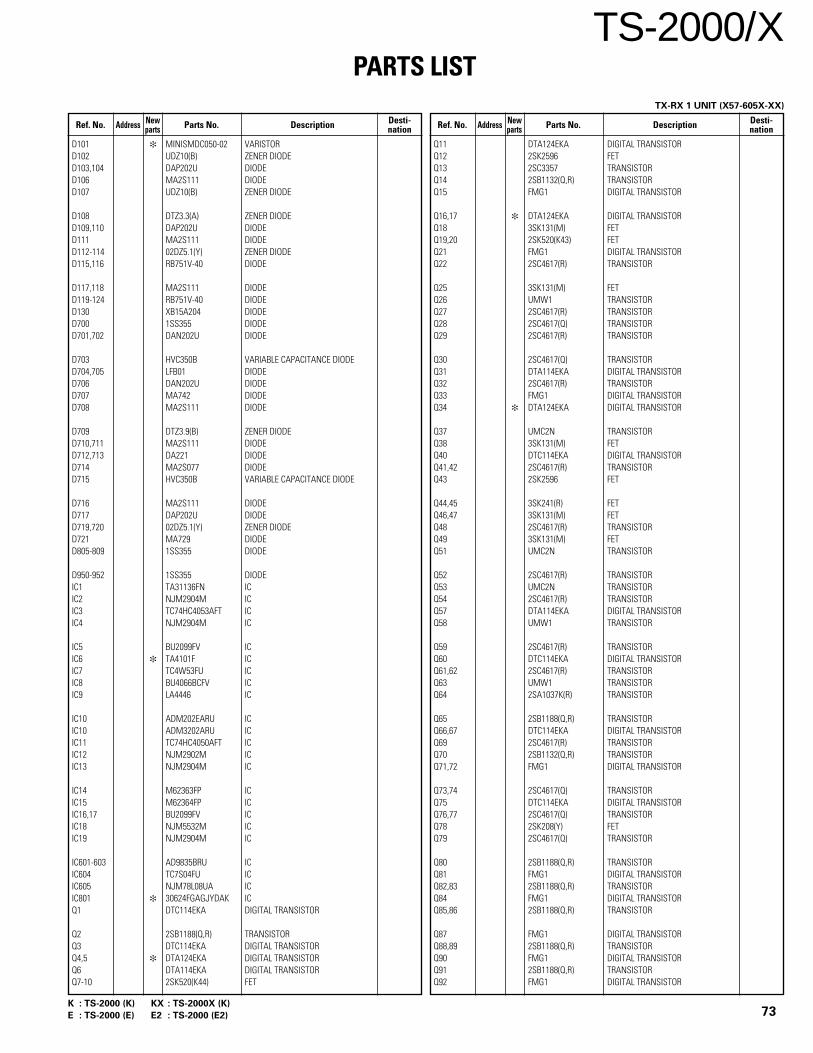
TS-2000/XPARTS LIST
73K : TS-2000 (K) KX : TS-2000X (K)
E : TS-2000 (E) E2 : TS-2000 (E2)
Ref. No. Address Parts No. Description Ref. No. Address Parts No. DescriptionNew Desti-parts nation
New Desti-parts nation
D101 MINISMDC050-02 VARISTORD102 UDZ10(B) ZENER DIODED103,104 DAP202U DIODED106 MA2S111 DIODED107 UDZ10(B) ZENER DIODE
D108 DTZ3.3(A) ZENER DIODED109,110 DAP202U DIODED111 MA2S111 DIODED112-114 02DZ5.1(Y) ZENER DIODED115,116 RB751V-40 DIODE
D117,118 MA2S111 DIODED119-124 RB751V-40 DIODED130 XB15A204 DIODED700 1SS355 DIODED701,702 DAN202U DIODE
D703 HVC350B VARIABLE CAPACITANCE DIODED704,705 LFB01 DIODED706 DAN202U DIODED707 MA742 DIODED708 MA2S111 DIODE
D709 DTZ3.9(B) ZENER DIODED710,711 MA2S111 DIODED712,713 DA221 DIODED714 MA2S077 DIODED715 HVC350B VARIABLE CAPACITANCE DIODE
D716 MA2S111 DIODED717 DAP202U DIODED719,720 02DZ5.1(Y) ZENER DIODED721 MA729 DIODED805-809 1SS355 DIODE
D950-952 1SS355 DIODEIC1 TA31136FN ICIC2 NJM2904M ICIC3 TC74HC4053AFT ICIC4 NJM2904M IC
IC5 BU2099FV ICIC6 TA4101F ICIC7 TC4W53FU ICIC8 BU4066BCFV ICIC9 LA4446 IC
IC10 ADM202EARU ICIC10 ADM3202ARU ICIC11 TC74HC4050AFT ICIC12 NJM2902M ICIC13 NJM2904M IC
IC14 M62363FP ICIC15 M62364FP ICIC16,17 BU2099FV ICIC18 NJM5532M ICIC19 NJM2904M IC
IC601-603 AD9835BRU ICIC604 TC7S04FU ICIC605 NJM78L08UA ICIC801 30624FGAGJYDAK ICQ1 DTC114EKA DIGITAL TRANSISTOR
Q2 2SB1188(Q,R) TRANSISTORQ3 DTC114EKA DIGITAL TRANSISTORQ4,5 DTA124EKA DIGITAL TRANSISTORQ6 DTA114EKA DIGITAL TRANSISTORQ7-10 2SK520(K44) FET
Q11 DTA124EKA DIGITAL TRANSISTORQ12 2SK2596 FETQ13 2SC3357 TRANSISTORQ14 2SB1132(Q,R) TRANSISTORQ15 FMG1 DIGITAL TRANSISTOR
Q16,17 DTA124EKA DIGITAL TRANSISTORQ18 3SK131(M) FETQ19,20 2SK520(K43) FETQ21 FMG1 DIGITAL TRANSISTORQ22 2SC4617(R) TRANSISTOR
Q25 3SK131(M) FETQ26 UMW1 TRANSISTORQ27 2SC4617(R) TRANSISTORQ28 2SC4617(Q) TRANSISTORQ29 2SC4617(R) TRANSISTOR
Q30 2SC4617(Q) TRANSISTORQ31 DTA114EKA DIGITAL TRANSISTORQ32 2SC4617(R) TRANSISTORQ33 FMG1 DIGITAL TRANSISTORQ34 DTA124EKA DIGITAL TRANSISTOR
Q37 UMC2N TRANSISTORQ38 3SK131(M) FETQ40 DTC114EKA DIGITAL TRANSISTORQ41,42 2SC4617(R) TRANSISTORQ43 2SK2596 FET
Q44,45 3SK241(R) FETQ46,47 3SK131(M) FETQ48 2SC4617(R) TRANSISTORQ49 3SK131(M) FETQ51 UMC2N TRANSISTOR
Q52 2SC4617(R) TRANSISTORQ53 UMC2N TRANSISTORQ54 2SC4617(R) TRANSISTORQ57 DTA114EKA DIGITAL TRANSISTORQ58 UMW1 TRANSISTOR
Q59 2SC4617(R) TRANSISTORQ60 DTC114EKA DIGITAL TRANSISTORQ61,62 2SC4617(R) TRANSISTORQ63 UMW1 TRANSISTORQ64 2SA1037K(R) TRANSISTOR
Q65 2SB1188(Q,R) TRANSISTORQ66,67 DTC114EKA DIGITAL TRANSISTORQ69 2SC4617(R) TRANSISTORQ70 2SB1132(Q,R) TRANSISTORQ71,72 FMG1 DIGITAL TRANSISTOR
Q73,74 2SC4617(Q) TRANSISTORQ75 DTC114EKA DIGITAL TRANSISTORQ76,77 2SC4617(Q) TRANSISTORQ78 2SK208(Y) FETQ79 2SC4617(Q) TRANSISTOR
Q80 2SB1188(Q,R) TRANSISTORQ81 FMG1 DIGITAL TRANSISTORQ82,83 2SB1188(Q,R) TRANSISTORQ84 FMG1 DIGITAL TRANSISTORQ85,86 2SB1188(Q,R) TRANSISTOR
Q87 FMG1 DIGITAL TRANSISTORQ88,89 2SB1188(Q,R) TRANSISTORQ90 FMG1 DIGITAL TRANSISTORQ91 2SB1188(Q,R) TRANSISTORQ92 FMG1 DIGITAL TRANSISTOR
TX-RX 1 UNIT (X57-605X-XX)

TS-2000/XPARTS LIST
74K : TS-2000 (K) KX : TS-2000X (K)
E : TS-2000 (E) E2 : TS-2000 (E2)
Ref. No. Address Parts No. Description Ref. No. Address Parts No. DescriptionNew Desti-parts nation
New Desti-parts nation
Q93-95 2SC4617(R) TRANSISTORQ96 FMG1 DIGITAL TRANSISTORQ97 2SD1624(S) TRANSISTORQ101-112 DTA114EKA DIGITAL TRANSISTORQ601-606 2SC4617(R) TRANSISTORQ607,608 DTC114EKA DIGITAL TRANSISTORQ609 DTC124EKA DIGITAL TRANSISTORQ700,701 3SK131(M) FET
Q702,703 DTC114EKA DIGITAL TRANSISTORQ704 DTC124EKA DIGITAL TRANSISTORQ705 2SK2596 FETQ706 2SB1132(Q,R) TRANSISTORQ707,708 FMG1 DIGITAL TRANSISTOR
Q709 2SC4617(Q) TRANSISTORQ710 2SC4617(S) TRANSISTORQ711 2SC4617(R) TRANSISTORQ712 DTC124EKA DIGITAL TRANSISTORQ714 DTC124EKA DIGITAL TRANSISTOR
Q715 2SC4617(R) TRANSISTORQ800 DTC114EE DIGITAL TRANSISTORQ801 2SA1641(S,T) TRANSISTORQ802 DTC114EE DIGITAL TRANSISTORQ803 2SC2712(Y) TRANSISTOR
Q804 DTC114EE DIGITAL TRANSISTORQ805 2SA1162(Y) TRANSISTORQ806 DTC114EE DIGITAL TRANSISTORQ808 DTC114EE DIGITAL TRANSISTORQ811 DTC114EE DIGITAL TRANSISTOR
Q813 DTC114EE DIGITAL TRANSISTORQ815 DTC114EE DIGITAL TRANSISTORQ817 DTC114EE DIGITAL TRANSISTORQ819,820 DTC114EE DIGITAL TRANSISTORQ822 DTC114EE DIGITAL TRANSISTOR
TH1,2 157-502-65001 THERMISTORTH3 157-302-65801 THERMISTORTH5,6 157-302-65801 THERMISTORTH7,8 157-102-65001 THERMISTORTH9 157-502-65001 THERMISTOR
S902 W02-1985-05 ENCODERS903 W02-1988-05 ENCODERS904 W02-1989-05 ENCODER
C1 CC73GCH1H120J CHIP C 12PF JC2 CC73GCH1H0R5B CHIP C 0.5PF BC3 CC73GCH1H040B CHIP C 4.0PF BC4 CC73GCH1H070B CHIP C 7.0PF BC5 CK73GB1H102K CHIP C 1000PF K
C6 CC73GCH1H120J CHIP C 12PF JC8 CC73GCH1H120J CHIP C 12PF J E,E2C8 CC73GCH1H220J CHIP C 22PF J K,KXC9-13 CK73GB1H102K CHIP C 1000PF KC14 CK73GB1H471K CHIP C 470PF K
C15 CK73GB1H102K CHIP C 1000PF KC16 CK73GB1H471K CHIP C 470PF KC18,19 CK73GB1H102K CHIP C 1000PF KC21 CK73GB1H471K CHIP C 470PF KC22 CK73GB1H102K CHIP C 1000PF K
C23,24 CK73GB1H471K CHIP C 470PF KC25,26 CC73GCH1H101J CHIP C 100PF J
C27 CK73GB1H471K CHIP C 470PF KC28 CK73GB1H102K CHIP C 1000PF KC29 CK73GB1H471K CHIP C 470PF KC30 CK73GB1C104K CHIP C 0.10UF KC31,32 CK73GB1H102K CHIP C 1000PF K
C33 CK73GB1H471K CHIP C 470PF KC34 CK73GB1H102K CHIP C 1000PF KC35 CK73GB1H103K CHIP C 0.010UF KC36,37 CK73GB1H102K CHIP C 1000PF KC39 CK73GB1H471K CHIP C 470PF K
C40 CK73GB1H102K CHIP C 1000PF KC41 C92-0625-05 ELECTRO 4.7UF 25WVC42 CK73GB1H102K CHIP C 1000PF KC43 CK73GB1H471K CHIP C 470PF KC44,45 CK73GB1H102K CHIP C 1000PF K
C46 CK73GB1H471K CHIP C 470PF KC47 CC73GCH1HR75B CHIP C 0.75PF BC48 CK73GB1H103K CHIP C 0.010UF KC49-51 CK73GB1H102K CHIP C 1000PF KC52 CC73GCH1H040B CHIP C 4.0PF B
C53 C92-0625-05 ELECTRO 4.7UF 25WVC54 CK73GB1H102K CHIP C 1000PF KC55 CK73GB1H471K CHIP C 470PF KC56 CK73GB1H102K CHIP C 1000PF KC57 CK73GB1H471K CHIP C 470PF K
C58,59 CK73GB1H102K CHIP C 1000PF KC60,61 CK73GB1H471K CHIP C 470PF KC62 CK73GB1H102K CHIP C 1000PF KC63 CC73GCH1H080B CHIP C 8.0PF BC64 CK73GB1H102K CHIP C 1000PF K
C65 CC73GCH1H390J CHIP C 39PF JC66 CC73GCH1H010B CHIP C 1.0PF BC67 CC73GCH1H100D CHIP C 10PF DC68 CK73GB1H471K CHIP C 470PF KC69 CC73GCH1H080B CHIP C 8.0PF B
C70 CC73GCH1H120J CHIP C 12PF JC71 CK73GB1H102K CHIP C 1000PF KC73 CK73GB1H103K CHIP C 0.010UF KC74,75 CK73GB1H102K CHIP C 1000PF KC76 CC73GCH1H070B CHIP C 7.0PF B
C77 CC73GCH1H0R3B CHIP C 0.3PF BC78 CK73GB1H471K CHIP C 470PF KC79 CC73GCH1H050B CHIP C 5.0PF BC80 CK73GB1H102K CHIP C 1000PF KC81 CK73GB1H471K CHIP C 470PF K
C82 CK73GB1H102K CHIP C 1000PF KC83 CC73GCH1H040B CHIP C 4.0PF BC84 CC73GCH1H150J CHIP C 15PF JC85 CK73GB1H102K CHIP C 1000PF KC86 CK73GB1H471K CHIP C 470PF K
C88 CK73GB1H102K CHIP C 1000PF KC91 CC73GCH1H060B CHIP C 6.0PF BC92 CC73GCH1H070B CHIP C 7.0PF BC94 CK73GB1H102K CHIP C 1000PF KC95 CC73GCH1H030B CHIP C 3.0PF B
C96 CK73GB1H471K CHIP C 470PF KC97 CC73GCH1H0R5B CHIP C 0.5PF BC98 CC73GCH1H040B CHIP C 4.0PF BC99 CC73GCH1H0R5B CHIP C 0.5PF BC100 CC73GCH1H040B CHIP C 4.0PF B
TX-RX 2 UNIT (X57-606X-XX) 0-11 : K,KX 2-71 : E,E2
TX-RX 1 UNIT (X57-605X-XX)
TX-RX 2 UNIT (X57-606X-XX)

TS-2000/XPARTS LIST
75K : TS-2000 (K) KX : TS-2000X (K)
E : TS-2000 (E) E2 : TS-2000 (E2)
Ref. No. Address Parts No. Description Ref. No. Address Parts No. DescriptionNew Desti-parts nation
New Desti-parts nation
C101 CK73GB1H471K CHIP C 470PF KC102 CC73GCH1H0R5B CHIP C 0.5PF BC103 CC73GCH1H0R3B CHIP C 0.3PF BC104 CC73GCH1H050B CHIP C 5.0PF BC105,106 CK73GB1H102K CHIP C 1000PF K
C107 CC73GCH1H050B CHIP C 5.0PF BC108 CC73GCH1H270J CHIP C 27PF JC109 CC73GCH1H070B CHIP C 7.0PF BC110 CK73GB1H103K CHIP C 0.010UF KC111 CC73GCH1H050B CHIP C 5.0PF B
C112 CC73GCH1H100D CHIP C 10PF DC113 CK73GB1H102K CHIP C 1000PF KC114 CK73GB1H471K CHIP C 470PF KC115 CC73GCH1H180J CHIP C 18PF JC116 CC73GCH1H0R3B CHIP C 0.3PF B
C117,118 CK73GB1H102K CHIP C 1000PF KC119 CC73GCH1H180J CHIP C 18PF JC120 CK73GB1H102K CHIP C 1000PF KC123 CK73GB1H102K CHIP C 1000PF KC124 CC73GCH1H120J CHIP C 12PF J
C125 CC73GCH1H060B CHIP C 6.0PF BC126 CK73GB1H102K CHIP C 1000PF KC127 CK73GB1H471K CHIP C 470PF KC128 CC73GCH1H020B CHIP C 2.0PF BC129 CK73GB1H471K CHIP C 470PF K
C130 CK73GB1H102K CHIP C 1000PF KC131-133 CK73GB1H471K CHIP C 470PF KC134 CC73GCH1H050B CHIP C 5.0PF BC135 CC73GCH1H060B CHIP C 6.0PF BC136,137 CK73GB1H102K CHIP C 1000PF K
C138 CK73GB1H471K CHIP C 470PF KC139,140 CK73GB1H102K CHIP C 1000PF KC141 CK73GB1H471K CHIP C 470PF KC142 CC73GCH1H040B CHIP C 4.0PF BC143,144 CK73GB1H102K CHIP C 1000PF K
C145 CK73GB1H471K CHIP C 470PF KC146 CC73GCH1H101J CHIP C 100PF JC147 CC73GCH1H080B CHIP C 8.0PF BC148 CC73GCH1H050B CHIP C 5.0PF BC150 CC73GCH1H0R5B CHIP C 0.5PF B
C151 CC73GCH1H120J CHIP C 12PF JC152 CK73GB1H471K CHIP C 470PF KC153 CC73GCH1H101J CHIP C 100PF JC154 CK73GB1H102K CHIP C 1000PF KC155 CC73GCH1H040B CHIP C 4.0PF B
C156 CK73GB1H102K CHIP C 1000PF KC157 CC73GCH1H040B CHIP C 4.0PF BC158 CC73GCH1H060B CHIP C 6.0PF BC159 CK73GB1H102K CHIP C 1000PF KC160 CC73GCH1H040B CHIP C 4.0PF B
C161 CK73GB1H471K CHIP C 470PF KC162,163 CC73GCH1H050B CHIP C 5.0PF BC164 CC73GCH1H0R5B CHIP C 0.5PF BC165 CC73GCH1H020B CHIP C 2.0PF BC166 CC73GCH1H070B CHIP C 7.0PF B
C167 CK73GB1H471K CHIP C 470PF KC168 CC73GCH1H040B CHIP C 4.0PF BC169 CK73GB1H102K CHIP C 1000PF KC170 CC73GCH1H060B CHIP C 6.0PF BC171 CC73GCH1H120J CHIP C 12PF J
C172 CC73GCH1H0R3B CHIP C 0.3PF BC173 CC73GCH1H030B CHIP C 3.0PF BC174,175 CK73GB1H102K CHIP C 1000PF KC176 CK73GB1H471K CHIP C 470PF KC177 CC73GCH1H470J CHIP C 47PF J
C178 CC73GCH1H0R3B CHIP C 0.3PF BC179 CC73GCH1H150J CHIP C 15PF JC180 CK73GB1H102K CHIP C 1000PF KC181 CC73GCH1H050B CHIP C 5.0PF BC182 CC73GCH1H090B CHIP C 9.0PF B
C183 CK73GB1H102K CHIP C 1000PF KC184 CK73GB1H471K CHIP C 470PF KC185 CC73GCH1H050B CHIP C 5.0PF BC186 CC73GCH1H0R3B CHIP C 0.3PF BC187 CK73GB1H103K CHIP C 0.010UF K
C188 CC73GCH1H100D CHIP C 10PF DC189 CC73GCH1H0R3B CHIP C 0.3PF BC190 CC73GCH1H100D CHIP C 10PF DC191 CK73FB1C105K CHIP C 1.0UF KC192 CC73GCH1H040B CHIP C 4.0PF B
C193,194 CK73GB1H102K CHIP C 1000PF KC195 CK73GB1H103K CHIP C 0.010UF KC196-199 CK73GB1H102K CHIP C 1000PF KC200,201 CK73GB1H471K CHIP C 470PF KC202,203 CC73GCH1H040B CHIP C 4.0PF B
C204 CC73GCH1H2R5B CHIP C 2.5PF BC205 CK73GB1H471K CHIP C 470PF KC206,207 CK73GB1H102K CHIP C 1000PF KC208,209 CK73GB1H471K CHIP C 470PF KC210 CK73FB1C105K CHIP C 1.0UF K
C211 CK73GB1H471K CHIP C 470PF KC212 CK73GB1H102K CHIP C 1000PF KC213 CK73GB1C104K CHIP C 0.10UF KC214-219 CK73GB1H102K CHIP C 1000PF KC220-222 CK73GB1C104K CHIP C 0.10UF K
C224 CC73GCH1H100D CHIP C 10PF DC225 CK73GB1C104K CHIP C 0.10UF KC227 CC73GCH1H020B CHIP C 2.0PF BC232 CK73GB1H102K CHIP C 1000PF KC233 CC73GCH1H220J CHIP C 22PF J
C234 CC73GCH1H270J CHIP C 27PF JC235 CK73GB1H102K CHIP C 1000PF KC238 CK73GB1H102K CHIP C 1000PF KC239 CK73GB1H471K CHIP C 470PF KC240 CC73GCH1H050B CHIP C 5.0PF B
C241 CC73GCH1H150J CHIP C 15PF JC242,243 CK73GB1H102K CHIP C 1000PF KC245 CK73GB1H102K CHIP C 1000PF KC246 CC73GCH1H030B CHIP C 3.0PF BC247 CK73GB1H471K CHIP C 470PF K
C248 CC73GCH1H150J CHIP C 15PF JC249 CC73GCH1H050B CHIP C 5.0PF B E,E2C249 CC73GCH1H100D CHIP C 10PF D K,KXC250 CK73GB1H471K CHIP C 470PF KC251 CK73GB1C104K CHIP C 0.10UF K
C252 CC73GCH1H070B CHIP C 7.0PF BC253 CK73GB1H103K CHIP C 0.010UF KC254 CC73GCH1H030B CHIP C 3.0PF BC255 CK73GB1H103K CHIP C 0.010UF KC256 CC73GCH1H120J CHIP C 12PF J
TX-RX 2 UNIT (X57-606X-XX)

TS-2000/XPARTS LIST
76K : TS-2000 (K) KX : TS-2000X (K)
E : TS-2000 (E) E2 : TS-2000 (E2)
Ref. No. Address Parts No. Description Ref. No. Address Parts No. DescriptionNew Desti-parts nation
New Desti-parts nation
C257 CK73GB1H102K CHIP C 1000PF KC258 CK73GB1H103K CHIP C 0.010UF KC259 CK73GB1H102K CHIP C 1000PF KC260 CK73GB1H103K CHIP C 0.010UF KC261 CK73GB1H102K CHIP C 1000PF K
C262,263 CK73GB1H103K CHIP C 0.010UF KC264,265 CK73GB1H102K CHIP C 1000PF KC266 CK73GB1H103K CHIP C 0.010UF KC267 CK73GB1C104K CHIP C 0.10UF KC268 CC73GCH1H390J CHIP C 39PF J
C269 CK73GB1H103K CHIP C 0.010UF KC270 CK73GB1H102K CHIP C 1000PF KC271 CC73GCH1H150J CHIP C 15PF JC272 CK73GB1H102K CHIP C 1000PF KC274 CK73GB1H471K CHIP C 470PF K
C276 CK73GB1H471K CHIP C 470PF KC277 CC73GCH1H150J CHIP C 15PF JC278 CK73GB1H103K CHIP C 0.010UF KC279 CC73GCH1H010B CHIP C 1.0PF BC280 CK73FB1C105K CHIP C 1.0UF K
C281 CK73GB1C104K CHIP C 0.10UF KC282 CC73GCH1H200J CHIP C 20PF JC283 CC73GCH1H030B CHIP C 3.0PF BC284-287 CK73GB1H103K CHIP C 0.010UF KC288 CK73GB1H102K CHIP C 1000PF K
C289 CK73GB1C104K CHIP C 0.10UF K E,E2C290-292 CK73GB1H103K CHIP C 0.010UF KC293,294 CK73FB1C105K CHIP C 1.0UF KC295 CK73GB1H103K CHIP C 0.010UF KC296 CC73GCH1H060B CHIP C 6.0PF B
C297,298 CK73GB1H103K CHIP C 0.010UF KC299 CK73GB1H471K CHIP C 470PF KC300 CK73GB1H102K CHIP C 1000PF KC301 CK73GB1H103K CHIP C 0.010UF KC303 CK73GB1C104K CHIP C 0.10UF K
C304-307 CK73GB1H103K CHIP C 0.010UF KC308,309 CK73GB1C104K CHIP C 0.10UF K E,E2C309 CK73GB1C104K CHIP C 0.10UF K K,KXC310 CK73GB1H103K CHIP C 0.010UF KC312 CK73GB1C104K CHIP C 0.10UF K
C314,315 CK73GB1H103K CHIP C 0.010UF KC316 CC73GCH1H120J CHIP C 12PF JC317,318 CK73GB1H103K CHIP C 0.010UF KC319 CC73GCH1H200J CHIP C 20PF JC320 CK73GB1H103K CHIP C 0.010UF K
C321 CC73GCH1H150J CHIP C 15PF JC322 CK73GB1H103K CHIP C 0.010UF KC323 C92-0610-05 ELECTRO 47UF 16WVC324 CK73GB1H103K CHIP C 0.010UF KC325 CK73GB1C104K CHIP C 0.10UF K
C326,327 CC73GCH1H030B CHIP C 3.0PF BC328 CK73GB1C104K CHIP C 0.10UF KC329,330 CK73GB1H103K CHIP C 0.010UF KC331 CK73GB1C104K CHIP C 0.10UF KC332 CK73GB1H102K CHIP C 1000PF K
C333 CK73GB1H103K CHIP C 0.010UF KC334 CK73GB1C104K CHIP C 0.10UF KC335 CC73GCH1H270J CHIP C 27PF JC336 CK73GB1C104K CHIP C 0.10UF KC338 CC73GCH1H221J CHIP C 220PF J
C339 CK73GB1H103K CHIP C 0.010UF KC340 CC73GCH1H221J CHIP C 220PF JC341 CK73GB1H471K CHIP C 470PF KC342,343 CK73GB1C104K CHIP C 0.10UF KC345 CK73GB1H103K CHIP C 0.010UF K
C346 CK73GB1C473K CHIP C 0.047UF KC347 CK73GB1H472K CHIP C 4700PF KC348 CC73GCH1H271J CHIP C 270PF JC349 CK73GB1C104K CHIP C 0.10UF KC350 CK73GB1H103K CHIP C 0.010UF K
C352 CK73GB1C473K CHIP C 0.047UF KC353 CK73GB1H103K CHIP C 0.010UF KC357 CK73GB1E223K CHIP C 0.022UF KC358 CK73GB1C473K CHIP C 0.047UF KC359 CK73GB1H103K CHIP C 0.010UF K
C360 CK73GB1C104K CHIP C 0.10UF KC361 CC73GCH1H330J CHIP C 33PF JC362 CK73FB1C105K CHIP C 1.0UF KC363 C92-0610-05 ELECTRO 47UF 16WVC364,365 CK73FB1C105K CHIP C 1.0UF K
C366 CK73GB1H103K CHIP C 0.010UF KC368 C92-0628-05 CHIP-TAN 10UF 10WVC372-375 CK73GB1H102K CHIP C 1000PF KC376 CC73GCH1H060B CHIP C 6.0PF BC377 CC73GCH1H330J CHIP C 33PF J
C378 CC73GCH1H060B CHIP C 6.0PF BC379 CC73GCH1H050B CHIP C 5.0PF BC382 CC73GCH1H050B CHIP C 5.0PF BC383 CK73GB1H102K CHIP C 1000PF KC384 CC73GCH1H0R5B CHIP C 0.5PF B
C385 CC73GCH1H010B CHIP C 1.0PF BC386 CC73GCH1H050B CHIP C 5.0PF BC387 CC73GCH1H180J CHIP C 18PF J K,KXC387 CC73GCH1H470J CHIP C 47PF J E,E2C389,390 CK73GB1C104K CHIP C 0.10UF K
C391 C92-0628-05 CHIP-TAN 10UF 10WVC393-399 CK73GB1H102K CHIP C 1000PF KC420 CK73GB1H472K CHIP C 4700PF KC421 C92-0628-05 CHIP-TAN 10UF 10WVC422 C92-0543-05 CHIP-TAN 3.3UF 10WV
C423,424 CK73GB1H102K CHIP C 1000PF KC425 C92-0628-05 CHIP-TAN 10UF 10WVC427 CC73GCH1H180J CHIP C 18PF JC428 CC73GCH1H100D CHIP C 10PF DC429 CK73GB1H102K CHIP C 1000PF K
C431 CK73GB1H102K CHIP C 1000PF KC432 C92-0543-05 CHIP-TAN 3.3UF 10WVC433 CK73GB1H471K CHIP C 470PF KC434 CC73GCH1H080B CHIP C 8.0PF BC435 CK73GB1H102K CHIP C 1000PF K
C436 CK73GB1H471K CHIP C 470PF KC437 CC73GCH1H060B CHIP C 6.0PF BC438 CK73GB1H102K CHIP C 1000PF KC439 CK73GB1C473K CHIP C 0.047UF KC440 CK73GB1H102K CHIP C 1000PF K
C441 CK73GB1C473K CHIP C 0.047UF KC442 C92-0628-05 CHIP-TAN 10UF 10WVC443 CC73GCH1H050B CHIP C 5.0PF BC444 CK73GB1C473K CHIP C 0.047UF KC445 CC73GCH1H030B CHIP C 3.0PF B
TX-RX 2 UNIT (X57-606X-XX)

TS-2000/XPARTS LIST
77K : TS-2000 (K) KX : TS-2000X (K)
E : TS-2000 (E) E2 : TS-2000 (E2)
Ref. No. Address Parts No. Description Ref. No. Address Parts No. DescriptionNew Desti-parts nation
New Desti-parts nation
C446 CC73GCH1H020B CHIP C 2.0PF BC447 CK73GB1H103K CHIP C 0.010UF KC448,449 CK73GB1H102K CHIP C 1000PF KC453 CC73GCH1H070B CHIP C 7.0PF BC454 CC73GCH1H150J CHIP C 15PF J
C455 CK73GB1H103K CHIP C 0.010UF KC456 CC73GCH1H180J CHIP C 18PF JC457 CC73GCH1H080B CHIP C 8.0PF BC458 CC73GCH1H070B CHIP C 7.0PF BC459,460 CK73GB1H102K CHIP C 1000PF K
C461 CK73GB1H472K CHIP C 4700PF KC462,463 CC73GCH1H180J CHIP C 18PF JC464 CK73GB1C473K CHIP C 0.047UF KC465,466 CK73GB1H102K CHIP C 1000PF KC467,468 CK73GB1H103K CHIP C 0.010UF K
C469,470 CC73GCH1H0R5B CHIP C 0.5PF BC471 C92-0628-05 CHIP-TAN 10UF 10WVC472 CC73GCH1H220J CHIP C 22PF JC473 C92-0628-05 CHIP-TAN 10UF 10WVC474 CK73GB1H471K CHIP C 470PF K
C475,476 CK73GB1H102K CHIP C 1000PF KC477 CK73GB1H103K CHIP C 0.010UF KC478,479 CK73GB1H471K CHIP C 470PF KC481,482 CC73GCH1H040B CHIP C 4.0PF BC483 CK73GB1H103K CHIP C 0.010UF K
C484 CK73GB1H102K CHIP C 1000PF KC485 C92-0628-05 CHIP-TAN 10UF 10WVC486,487 CC73GCH1H060B CHIP C 6.0PF BC488 CC73GCH1H390J CHIP C 39PF JC489 CK73GB1H103K CHIP C 0.010UF K
C490 CK73GB1H472K CHIP C 4700PF KC491,492 CC73GCH1H050B CHIP C 5.0PF BC494 CK73GB1H103K CHIP C 0.010UF KC495 CC73GCH1H470J CHIP C 47PF JC496 CK73GB1H102K CHIP C 1000PF K
C497 CC73GCH1H060B CHIP C 6.0PF BC498 CK73GB1H102K CHIP C 1000PF KC499 CC73GCH1H060B CHIP C 6.0PF BC501 CK73GB1H471K CHIP C 470PF KC502 C92-0628-05 CHIP-TAN 10UF 10WV
C503 CK73GB1H472K CHIP C 4700PF KC504 CK73GB1C473K CHIP C 0.047UF KC505 CC73GCH1H270J CHIP C 27PF JC506 CC73GCH1H040B CHIP C 4.0PF BC507 CK73GB1H103K CHIP C 0.010UF K
C508 CC73GCH1H470J CHIP C 47PF JC509 CK73GB1H471K CHIP C 470PF KC510 CC73GCH1H101J CHIP C 100PF JC511 CK73GB1H471K CHIP C 470PF KC512 CC73GCH1H390J CHIP C 39PF J
C513 C92-0001-05 CHIP C 0.1UF 35WVC514 C92-0004-05 CHIP-TAN 1.0UF 16WVC515 CC73GCH1H101J CHIP C 100PF JC516 C92-0003-05 CHIP-TAN 0.47UF 25WVC517 CC73GCH1H151J CHIP C 150PF J
C518 C92-0555-05 CHIP-TAN 0.047UF 35WVC519 CK73GB1C473K CHIP C 0.047UF KC520 CC73GCH1H151J CHIP C 150PF JC521 CK73GB1C473K CHIP C 0.047UF KC522 CC73GCH1H151J CHIP C 150PF J
C523 CK73GB1H472K CHIP C 4700PF KC524 CC73GCH1H470J CHIP C 47PF JC525 CC73GCH1H100D CHIP C 10PF DC526 CK73GB1H102K CHIP C 1000PF KC527 CK73GB1C473K CHIP C 0.047UF K
C528 C92-0628-05 CHIP-TAN 10UF 10WVC529 CK73GB1H472K CHIP C 4700PF KC530 CC73GCH1H070B CHIP C 7.0PF BC531 CK73GB1C473K CHIP C 0.047UF KC532 CC73GCH1H270J CHIP C 27PF J
C533 CC73GCH1H101J CHIP C 100PF JC534 C92-1327-05 CHIP-TAN 100UF 10WVC535 CC73GCH1H820J CHIP C 82PF JC536 CK73GB1C473K CHIP C 0.047UF KC537 CC73GCH1H020B CHIP C 2.0PF B
C538 CK73GB1C473K CHIP C 0.047UF KC539 C92-0628-05 CHIP-TAN 10UF 10WVC540 CC73GCH1H150J CHIP C 15PF JC541 CK73GB1C473K CHIP C 0.047UF KC542 CC73GCH1H101J CHIP C 100PF J
C543 CC73GCH1H080B CHIP C 8.0PF BC544 CK73GB1H472K CHIP C 4700PF KC545 CK73GB1H102K CHIP C 1000PF KC546 C92-1327-05 CHIP-TAN 100UF 10WVC547 CC73GCH1H470J CHIP C 47PF J
C548 CC73GCH1H010B CHIP C 1.0PF BC549 CC73GCH1H390J CHIP C 39PF JC550 CK73GB1H102K CHIP C 1000PF KC551 CC73GCH1H121J CHIP C 120PF JC552 CK73GB1H102K CHIP C 1000PF K
C554 CK73GB1H103K CHIP C 0.010UF KC555 CC73GCH1H070B CHIP C 7.0PF BC556 CC73GCH1H181J CHIP C 180PF JC558 CK73GB1H103K CHIP C 0.010UF KC559,560 CK73GB1C473K CHIP C 0.047UF K
C561 CC73GCH1H150J CHIP C 15PF JC562 CC73GCH1H470J CHIP C 47PF JC563 CC73GCH1H151J CHIP C 150PF JC564 CC73GCH1H101J CHIP C 100PF JC565 CK73GB1H103K CHIP C 0.010UF K
C566 CC73GCH1H101J CHIP C 100PF JC567 CK73GB1H103K CHIP C 0.010UF KC568 CK73GB1H472K CHIP C 4700PF KC569 CC73GCH1H470J CHIP C 47PF JC570 CC73GCH1H151J CHIP C 150PF J
C571 CK73GB1H332K CHIP C 3300PF KC572,573 CK73GB1C473K CHIP C 0.047UF KC574 C92-0628-05 CHIP-TAN 10UF 10WVC576 CK73GB1H472K CHIP C 4700PF KC577 C92-0628-05 CHIP-TAN 10UF 10WV
C579 CK73GB1H472K CHIP C 4700PF KC580 CK73GB1C473K CHIP C 0.047UF KC581 CC73GCH1H220J CHIP C 22PF JC582 CC73GCH1H181J CHIP C 180PF JC583 C92-0628-05 CHIP-TAN 10UF 10WV
C585 CK73GB1H472K CHIP C 4700PF KC586-588 CK73GB1H103K CHIP C 0.010UF KC589,590 CK73GB1H102K CHIP C 1000PF KC591 CC73GCH1H390J CHIP C 39PF JC592 CC73GCH1H270J CHIP C 27PF J
TX-RX 2 UNIT (X57-606X-XX)

TS-2000/XPARTS LIST
78K : TS-2000 (K) KX : TS-2000X (K)
E : TS-2000 (E) E2 : TS-2000 (E2)
Ref. No. Address Parts No. Description Ref. No. Address Parts No. DescriptionNew Desti-parts nation
New Desti-parts nation
C593-595 CK73GB1H103K CHIP C 0.010UF KC596,597 C92-0628-05 CHIP-TAN 10UF 10WVC598,599 CK73GB1C473K CHIP C 0.047UF KC600 CK73GB1H102K CHIP C 1000PF KC601 CC73GCH1H020B CHIP C 2.0PF B
C602 C92-1327-05 CHIP-TAN 100UF 10WVC603 CK73GB1C473K CHIP C 0.047UF KC605,606 CK73GB1C473K CHIP C 0.047UF KC607,608 CC73GCH1H560J CHIP C 56PF JC609 CC73GCH1H150J CHIP C 15PF J
C610,611 CC73GCH1H240J CHIP C 24PF JC612 CK73GB1H103K CHIP C 0.010UF KC613 CC73GCH1H101J CHIP C 100PF JC614 CC73GCH1H100D CHIP C 10PF DC615 CC73GCH1H101J CHIP C 100PF J
C616,617 CK73GB1C473K CHIP C 0.047UF KC618,619 CC73GCH1H100D CHIP C 10PF DC620 C92-0628-05 CHIP-TAN 10UF 10WVC621-623 CK73GB1C473K CHIP C 0.047UF KC625 CK73GB1C473K CHIP C 0.047UF K
C626 CC73GCH1H560J CHIP C 56PF JC627 CC73GCH1H101J CHIP C 100PF JC628 CC73GCH1H040B CHIP C 4.0PF BC629 CC73GCH1H101J CHIP C 100PF JC630 CC73GCH1H820J CHIP C 82PF J
C631 CC73GCH1H240J CHIP C 24PF JC632,633 CC73GCH1H030B CHIP C 3.0PF BC634 CC73GCH1H470J CHIP C 47PF JC636 CC73GCH1H390J CHIP C 39PF JC637 CK73GB1C473K CHIP C 0.047UF K
C638 CC73GCH1H070B CHIP C 7.0PF BC639 CK73GB1C473K CHIP C 0.047UF KC640 CC73GCH1H101J CHIP C 100PF JC641 CC73GCH1H560J CHIP C 56PF JC642 CK73GB1C473K CHIP C 0.047UF K
C643 CC73GCH1H560J CHIP C 56PF JC644 CC73GCH1H820J CHIP C 82PF JC645 CK73GB1C473K CHIP C 0.047UF KC646 CK73GB1H102K CHIP C 1000PF KC647 CC73GCH1H120J CHIP C 12PF J
C648 CK73GB1H102K CHIP C 1000PF KC649 CK73GB1C473K CHIP C 0.047UF KC650 CC73GCH1H100D CHIP C 10PF DC651 CC73GCH1H101J CHIP C 100PF JC652 CC73GCH1H060B CHIP C 6.0PF B
C654 CC73GCH1H030B CHIP C 3.0PF BC656 CK73GB1H471K CHIP C 470PF KC657 CC73GCH1H080B CHIP C 8.0PF BC658 CC73GCH1H0R5B CHIP C 0.5PF BC659 CC73GCH1H560J CHIP C 56PF J
C660 CK73GB1H332K CHIP C 3300PF KC662 CK73GB1H472K CHIP C 4700PF KC663 CC73GCH1H120J CHIP C 12PF JC665 CK73GB1C473K CHIP C 0.047UF KC666 CK73GB1H472K CHIP C 4700PF K
C667,668 CK73GB1C473K CHIP C 0.047UF KC669 CK73GB1H102K CHIP C 1000PF KC670 CC73GCH1H0R5B CHIP C 0.5PF BC671 CC73GCH1H390J CHIP C 39PF JC672 CK73GB1H102K CHIP C 1000PF K
C674 CC73GCH1H101J CHIP C 100PF JC675 CK73GB1H471K CHIP C 470PF KC676 CK73GB1C473K CHIP C 0.047UF KC677 CC73GCH1H151J CHIP C 150PF JC679 CK73GB1C473K CHIP C 0.047UF K
C680 CK73GB1H102K CHIP C 1000PF KC681 CC73GCH1H070B CHIP C 7.0PF BC682 CK73GB1H471K CHIP C 470PF KC683 CK73GB1H102K CHIP C 1000PF KC684 CK73GB1H471K CHIP C 470PF K
C685 CC73GCH1H020B CHIP C 2.0PF BC686 C92-0511-05 CHIP-TAN 0.15UF 35WVC687 CK73GB1H102K CHIP C 1000PF KC688 CC73GCH1H150J CHIP C 15PF JC689 CK73GB1H102K CHIP C 1000PF K
C690 CC73GCH1H070B CHIP C 7.0PF BC691 CK73GB1H103K CHIP C 0.010UF KC693,694 CK73GB1H472K CHIP C 4700PF KC695 CC73GCH1H060B CHIP C 6.0PF BC696 CK73GB1H102K CHIP C 1000PF K
C698,699 C92-0628-05 CHIP-TAN 10UF 10WVC700 CC73GCH1H150J CHIP C 15PF JC701 CC73GCH1H270J CHIP C 27PF JC702 CC73GCH1H180J CHIP C 18PF JC705 CK73GB1H102K CHIP C 1000PF K
C706 CK73GB1H103K CHIP C 0.010UF KC707 CK73GB1H102K CHIP C 1000PF KC708,709 CK73GB1C473K CHIP C 0.047UF KC712 CC73GCH1H020B CHIP C 2.0PF BC714 CK73GB1H103K CHIP C 0.010UF K
C715 CK73GB1C473K CHIP C 0.047UF KC716 CK73GB1H103K CHIP C 0.010UF KC717 C92-0628-05 CHIP-TAN 10UF 10WVC718 CK73GB1C473K CHIP C 0.047UF KC720,721 C92-0628-05 CHIP-TAN 10UF 10WV
C722,723 CC73GCH1H151J CHIP C 150PF JC724,725 CK73GB1C473K CHIP C 0.047UF KC726 C92-1327-05 CHIP-TAN 100UF 10WVC728 C92-0555-05 CHIP-TAN 0.047UF 35WVC729 CK73GB1C473K CHIP C 0.047UF K
C731 CC73GCH1H820J CHIP C 82PF JC733 CK73GB1H102K CHIP C 1000PF KC734 CC73GCH1H390J CHIP C 39PF JC736 C92-0628-05 CHIP-TAN 10UF 10WVC737 CC73GCH1H820J CHIP C 82PF J
C739 C92-0543-05 CHIP-TAN 3.3UF 10WVC740 CK73GB1H102K CHIP C 1000PF KC741 CC73GCH1H220J CHIP C 22PF JC742 CC73GCH1H240J CHIP C 24PF JC743 C92-0543-05 CHIP-TAN 3.3UF 10WV
C744 CK73GB1H103K CHIP C 0.010UF KC745 CC73GCH1H270J CHIP C 27PF JC746 CK73GB1H102K CHIP C 1000PF KC747 C92-0628-05 CHIP-TAN 10UF 10WVC748 CK73GB1H102K CHIP C 1000PF K
C749 CK73GB1H471K CHIP C 470PF KC750 CK73GB1C473K CHIP C 0.047UF KC751,752 C92-0543-05 CHIP-TAN 3.3UF 10WVC753,754 CK73GB1H182K CHIP C 1800PF KC755 CC73GCH1H180J CHIP C 18PF J
TX-RX 2 UNIT (X57-606X-XX)

TS-2000/XPARTS LIST
79K : TS-2000 (K) KX : TS-2000X (K)
E : TS-2000 (E) E2 : TS-2000 (E2)
Ref. No. Address Parts No. Description Ref. No. Address Parts No. DescriptionNew Desti-parts nation
New Desti-parts nation
C756 CC73GCH1H100D CHIP C 10PF DC757 CK73GB1C473K CHIP C 0.047UF KC758 CK73GB1H471K CHIP C 470PF KC759 CK73GB1H472K CHIP C 4700PF KC761 CC73GCH1H101J CHIP C 100PF J
C762 CK73GB1H102K CHIP C 1000PF KC763,764 CC73GCH1H180J CHIP C 18PF JC765,766 CC73GCH1H100D CHIP C 10PF DC767 C92-0628-05 CHIP-TAN 10UF 10WVC770 CK73GB1H103K CHIP C 0.010UF K
C771 C92-0628-05 CHIP-TAN 10UF 10WVC772 CC73GCH1H101J CHIP C 100PF JC773,774 CK73GB1H103K CHIP C 0.010UF KC775 CK73GB1H102K CHIP C 1000PF KC776 CK73GB1H471K CHIP C 470PF K
C777 C92-0555-05 CHIP-TAN 0.047UF 35WVC778 CK73GB1H102K CHIP C 1000PF KC780 CK73GB1H471K CHIP C 470PF KC781 CC73GCH1H100D CHIP C 10PF DC782 CC73GCH1H050B CHIP C 5.0PF B
C783 CK73GB1H103K CHIP C 0.010UF KC784 CK73GB1H102K CHIP C 1000PF KC786 CK73GB1H103K CHIP C 0.010UF KC788 CK73GB1H103K CHIP C 0.010UF KC789,790 CC73GCH1H101J CHIP C 100PF J
C791 CK73GB1H103K CHIP C 0.010UF KC792 CK73GB1H471K CHIP C 470PF KC793 C92-0606-05 CHIP-TAN 4.7UF 10WVC794 CK73GB1H472K CHIP C 4700PF KC795 C92-0628-05 CHIP-TAN 10UF 10WV
C796 CK73GB1C473K CHIP C 0.047UF KC798 CK73GB1H471K CHIP C 470PF KC799 C92-0502-05 CHIP-TAN 0.33UF 35WVC800 C92-0511-05 CHIP-TAN 0.15UF 35WVC802,803 CK73GB1C473K CHIP C 0.047UF K
C804 CC73GCH1H101J CHIP C 100PF JC806 CK73GB1C473K CHIP C 0.047UF KC807 CC73GCH1H220J CHIP C 22PF JC808 CK73GB1H102K CHIP C 1000PF KC809 CK73GB1C473K CHIP C 0.047UF K
C810 CK73GB1H471K CHIP C 470PF KC811 CC73GCH1H101J CHIP C 100PF JC813 CC73GCH1H220J CHIP C 22PF JC814 CK73GB1H102K CHIP C 1000PF KC815 CK73GB1C473K CHIP C 0.047UF K
C817 CK73GB1H102K CHIP C 1000PF KC818 CC73GCH1H120J CHIP C 12PF JC819 CK73GB1H472K CHIP C 4700PF KC820 CK73GB1H102K CHIP C 1000PF KC821,822 CC73GCH1H120J CHIP C 12PF J
C823 CC73GCH1H240J CHIP C 24PF JC824 CC73GCH1H180J CHIP C 18PF JC825 CK73GB1H103K CHIP C 0.010UF KC826 CC73GCH1H240J CHIP C 24PF JC827,828 CK73GB1H102K CHIP C 1000PF K
C830 CK73GB1H102K CHIP C 1000PF KC831 CK73GB1H471K CHIP C 470PF KC832 CK73GB1H102K CHIP C 1000PF KC835 CC73GCH1H100D CHIP C 10PF DC836 CK73GB1H103K CHIP C 0.010UF K
C839 CK73GB1C473K CHIP C 0.047UF KC840-842 CK73GB1H103K CHIP C 0.010UF KC844 C92-1327-05 CHIP-TAN 100UF 10WVC849-854 C92-0628-05 CHIP-TAN 10UF 10WVC857-859 CK73GB1H102K CHIP C 1000PF K
C860 C92-0628-05 CHIP-TAN 10UF 10WVC861,862 CK73GB1H102K CHIP C 1000PF KC863,864 CK73GB1H471K CHIP C 470PF KC865 CK73GB1H102K CHIP C 1000PF KC866,867 CK73GB1H103K CHIP C 0.010UF K
C868 C92-0628-05 CHIP-TAN 10UF 10WVC869,870 CK73GB1H102K CHIP C 1000PF KC871 CK73GB1H472K CHIP C 4700PF KC872,873 CK73GB1H102K CHIP C 1000PF KC874 CK73GB1C473K CHIP C 0.047UF K
C875 CK73GB1H103K CHIP C 0.010UF KC876 CC73GCH1H151J CHIP C 150PF JC877,878 CC73GCH1H070B CHIP C 7.0PF BC879 CK73GB1H471K CHIP C 470PF KC880 CC73GCH1H020B CHIP C 2.0PF B
C881 CK73GB1H471K CHIP C 470PF KC882 CC73GCH1H020B CHIP C 2.0PF BC883,884 CC73GCH1H150J CHIP C 15PF JC885 CK73GB1H102K CHIP C 1000PF KC886,887 CC73GCH1H150J CHIP C 15PF J
C888,889 CC73GCH1H010B CHIP C 1.0PF BC890 CC73GCH1H270J CHIP C 27PF JC892,893 CC73GCH1H070B CHIP C 7.0PF BC894,895 CC73GCH1H060B CHIP C 6.0PF BC896 CK73GB1H103K CHIP C 0.010UF K
C897 CC73GCH1H120J CHIP C 12PF JC898 CK73GB1H471K CHIP C 470PF KC899,900 CC73GCH1H330J CHIP C 33PF JC901 CK73GB1H471K CHIP C 470PF KC902 CC73GCH1H050B CHIP C 5.0PF B
C903 CK73GB1H471K CHIP C 470PF KC904 CC73GCH1H050B CHIP C 5.0PF BC905 CC73GCH1H070B CHIP C 7.0PF BC906 C92-0628-05 CHIP-TAN 10UF 10WVC907,908 CC73GCH1H020B CHIP C 2.0PF B
C909,910 CK73GB1H102K CHIP C 1000PF KC911 CC73GCH1H150J CHIP C 15PF JC912 CK73GB1H471K CHIP C 470PF KC913 CK73GB1H102K CHIP C 1000PF KC914 CC73GCH1H150J CHIP C 15PF J
C915 CK73GB1H471K CHIP C 470PF KC916,917 CC73GCH1H040B CHIP C 4.0PF BC918 CC73GCH1H560J CHIP C 56PF JC919,920 CK73GB1H102K CHIP C 1000PF KC923 CK73GB1H471K CHIP C 470PF K
C924 CK73GB1H472K CHIP C 4700PF KC925,926 CC73GCH1H050B CHIP C 5.0PF BC927 CC73GCH1H020B CHIP C 2.0PF BC928 CK73GB1H472K CHIP C 4700PF KC929 CK73GB1H102K CHIP C 1000PF K
C930 CC73GCH1H050B CHIP C 5.0PF BC931 CK73GB1H472K CHIP C 4700PF KC932 CC73GCH1H270J CHIP C 27PF JC933 CK73GB1H102K CHIP C 1000PF KC934,935 CK73GB1H471K CHIP C 470PF K
TX-RX 2 UNIT (X57-606X-XX)

TS-2000/XPARTS LIST
80K : TS-2000 (K) KX : TS-2000X (K)
E : TS-2000 (E) E2 : TS-2000 (E2)
Ref. No. Address Parts No. Description Ref. No. Address Parts No. DescriptionNew Desti-parts nation
New Desti-parts nation
C936 CC73GCH1H330J CHIP C 33PF JTC1-6 C05-0369-05 CERAMIC TRIMMER CAPTC8-10 C05-0369-05 CERAMIC TRIMMER CAPTC12 C05-0370-05 CERAMIC TRIMMER CAPTC13 C05-0369-05 CERAMIC TRIMMER CAP
TC14 C05-0370-05 CERAMIC TRIMMER CAPTC400,401 C05-0346-05 CERAMIC TRIMMER CAP (6P)TC402 C05-0384-05 CERAMIC TRIMMER CAP (10P)TC403 C05-0356-05 CERAMIC TRIMMER CAP (20P)TC404,405 C05-0384-05 CERAMIC TRIMMER CAP (10P)
TC406 C05-0356-05 CERAMIC TRIMMER CAP (20P)TC408-410 C05-0384-05 CERAMIC TRIMMER CAP (10P)
CN1-4 E04-0191-05 PIN SOCKETCN6 E04-0191-05 PIN SOCKETCN7 E40-3247-05 PIN ASSYCN8 E04-0191-05 PIN SOCKETCN9 E40-3246-05 PIN ASSY
CN10 E40-3237-05 PIN ASSYCN11 E04-0191-05 PIN SOCKETCN12 E40-5741-05 FLAT CABLE CONNECTORCN13 E04-0191-05 PIN SOCKETCN14 E40-5978-05 FLAT CABLE CONNECTOR
CN15 E04-0154-05 PIN SOCKETCN17 E40-5978-05 FLAT CABLE CONNECTORCN18 E04-0191-05 PIN SOCKETCN19 E04-0154-05 PIN SOCKETCN501 E40-5740-05 FLAT CABLE CONNECTOR
CN502-506 E04-0191-05 PIN SOCKETCN510 E40-5699-05 PIN ASSYCN511,512 E40-6019-05 PIN ASSYCN513 E40-5699-05 PIN ASSYCN514 E40-6019-05 PIN ASSY
CN530 E40-3246-05 PIN ASSYCN532 E40-5699-05 PIN ASSYCN533,534 E40-5758-05 FLAT CABLE CONNECTORCN535 E40-5699-05 PIN ASSYJ1 E11-0438-05 PHONE JACK (9P)
J2 E11-0455-05 3.5D PHONE JACK (3P)W1 E37-0885-15 LEAD WIRE WITH CONNECTORW501 E37-0956-05 LEAD WIRE WITH CONNECTORW503 E37-0955-05 LEAD WIRE WITH CONNECTOR
- F10-2345-04 SHIELDING CASE- F10-2346-04 SHIELDING CASE- F10-2347-04 SHIELDING CASE- F10-2348-04 SHIELDING CASE- F10-2349-14 SHIELDING CASE
401 1B F10-2351-04 SHIELDING COVER- F10-2388-14 SHIELDING CASE402 1B F10-2389-04 SHIELDING COVER- F10-2390-04 SHIELDING CASE- F10-2391-04 SHIELDING CASE
- G02-0794-04 FLAT SPRING- G13-1789-04 CUSHION- G13-1790-04 CUSHION
CF1 L72-0984-05 CERAMIC FILTERCF2 L72-0986-05 CERAMIC FILTER E,E2CF400 L72-0343-05 CERAMIC FILTERL1 L40-1095-34 SMALL FIXED INDUCTOR (1UH)L4,5 L92-0180-05 FERRITE CHIP
L6 L40-8275-92 SMALL FIXED INDUCTOR (82NH)L7 L40-2785-92 SMALL FIXED INDUCTOR (270NH)L8,9 L39-1421-05 TOROIDAL COILL10 L40-1575-92 SMALL FIXED INDUCTOR (15NH)L11 L40-1085-92 SMALL FIXED INDUCTOR (100NH)
L12,13 L40-1875-92 SMALL FIXED INDUCTOR (18NH)L14,15 L40-4775-92 SMALL FIXED INDUCTOR (47NH)L22 L40-1095-34 SMALL FIXED INDUCTOR (1UH)L23 L34-4472-05 COILL27 L40-4775-34 SMALL FIXED INDUCTOR (47NH)
L28 L34-4472-05 COILL29 L79-1574-05 FILTER MODULE E,E2L29 L79-1575-05 FILTER MODULE K,KXL31 L40-1575-92 SMALL FIXED INDUCTOR (15NH)L32 L40-6875-34 SMALL FIXED INDUCTOR (68NH)
L34 L34-4472-05 COILL35 L40-6875-34 SMALL FIXED INDUCTOR (68NH)L39 L40-2275-92 SMALL FIXED INDUCTOR (22NH)L43 L40-8275-92 SMALL FIXED INDUCTOR (82NH)L44 L34-4472-05 COIL
L45 L40-1875-92 SMALL FIXED INDUCTOR (18NH)L46 L40-1075-92 SMALL FIXED INDUCTOR (10NH)L47 L34-4472-05 COILL48 L40-3375-34 SMALL FIXED INDUCTOR (33NH)L50 L79-1574-05 FILTER MODULE E,E2
L50 L79-1575-05 FILTER MODULE K,KXL52 L34-4472-05 COILL55 L34-4472-05 COILL59 L39-1421-05 TOROIDAL COILL61-63 L39-1421-05 TOROIDAL COIL
L64,65 L92-0138-05 FERRITE CHIPL66-68 L39-1421-05 TOROIDAL COILL69 L40-3381-37 SMALL FIXED INDUCTOR (0.330UH)L72 L40-3381-37 SMALL FIXED INDUCTOR (0.330UH)L73 L40-5675-92 SMALL FIXED INDUCTOR (56NH)
L74 L40-3381-37 SMALL FIXED INDUCTOR (0.330UH)L75 L39-1421-05 TOROIDAL COILL79 L40-5681-37 SMALL FIXED INDUCTOR (0.560UH)L80 L34-4205-05 COILL82 L34-4206-05 COIL
L83 L40-4705-85 SMALL FIXED INDUCTOR (47U)L85 L40-4705-85 SMALL FIXED INDUCTOR (47U)L86 L34-4649-05 COILL89 L40-6885-34 SMALL FIXED INDUCTOR (680NH)L90 L34-4026-15 COIL
L91 L34-4025-05 COILL93 L34-4459-05 COILL95-97 L40-1085-92 SMALL FIXED INDUCTOR (100NH)L100 L41-3391-04 SMALL FIXED INDUCTORL101 L92-0180-05 FERRITE CHIP
L102 L41-3391-04 SMALL FIXED INDUCTORL103-105 L40-5685-34 SMALL FIXED INDUCTOR (560NH)L106 L40-1875-34 SMALL FIXED INDUCTOR (18NH)L108,109 L34-4604-05 AIR-CORE COILL110 L34-4605-05 AIR-CORE COIL
L111 L34-4603-05 AIR-CORE COILL116 L34-4604-05 AIR-CORE COILL117 L34-4605-05 AIR-CORE COILL118,119 L34-4604-05 AIR-CORE COILL121,122 L40-6865-92 SMALL FIXED INDUCTOR (6.8NH)
TX-RX 2 UNIT (X57-606X-XX)

TS-2000/XPARTS LIST
81K : TS-2000 (K) KX : TS-2000X (K)
E : TS-2000 (E) E2 : TS-2000 (E2)
Ref. No. Address Parts No. Description Ref. No. Address Parts No. DescriptionNew Desti-parts nation
New Desti-parts nation
L123 L34-4605-05 AIR-CORE COILL124 L40-4763-92 SMALL FIXED INDUCTOR (4.7NH)L125 L40-1575-92 SMALL FIXED INDUCTOR (15NH)L128 L34-4605-05 AIR-CORE COILL129 L34-4603-05 AIR-CORE COIL
L130 L41-3391-04 SMALL FIXED INDUCTORL131 L40-5675-92 SMALL FIXED INDUCTOR (56NH)L132 L40-1875-34 SMALL FIXED INDUCTOR (18NH)L133 L34-4605-05 AIR-CORE COILL134 L40-1085-92 SMALL FIXED INDUCTOR (100NH)
L137 L34-4603-05 AIR-CORE COILL139 L40-4775-92 SMALL FIXED INDUCTOR (47NH)L140 L40-8265-92 SMALL FIXED INDUCTOR (8.2NH)L141 L34-4604-05 AIR-CORE COILL142-144 L40-1085-92 SMALL FIXED INDUCTOR (100NH)
L145 L40-1585-92 SMALL FIXED INDUCTOR (150NH)L146 L40-4775-92 SMALL FIXED INDUCTOR (47NH)L147 L40-5685-34 SMALL FIXED INDUCTOR (560NH)L148 L40-1095-34 SMALL FIXED INDUCTOR (1UH)L149 L40-4775-34 SMALL FIXED INDUCTOR (47NH)
L151 L40-1585-92 SMALL FIXED INDUCTOR (150NH)L154 L40-1085-92 SMALL FIXED INDUCTOR (100NH)L155 L40-2785-34 SMALL FIXED INDUCTOR (270NH)L156 L40-3985-34 SMALL FIXED INDUCTOR (390NH)L157 L40-6885-34 SMALL FIXED INDUCTOR (680NH)
L158 L40-1575-34 SMALL FIXED INDUCTOR (15NH)L159 L41-3391-04 SMALL FIXED INDUCTORL160 L40-1585-92 SMALL FIXED INDUCTOR (150NH)L161 L40-4775-92 SMALL FIXED INDUCTOR (47NH)L162 L40-6875-92 SMALL FIXED INDUCTOR (68NH)
L163,164 L34-4080-05 COILL165 L40-2285-92 SMALL FIXED INDUCTOR (220NH)L166,167 L40-4785-34 SMALL FIXED INDUCTOR (470NH)L168 L40-1085-92 SMALL FIXED INDUCTOR (100NH)L169 L40-1085-34 SMALL FIXED INDUCTOR (100NH)
L170 L40-1575-92 SMALL FIXED INDUCTOR (15NH)L171 L40-4791-37 SMALL FIXED INDUCTOR (4.700UH)L172 L40-5685-34 SMALL FIXED INDUCTOR (560NH)L400,401 L41-2791-04 SMALL FIXED INDUCTORL402,403 L34-4572-05 AIR-CORE COIL
L404 L40-1085-92 SMALL FIXED INDUCTOR (100NH)L405 L40-1075-92 SMALL FIXED INDUCTOR (10NH)L406 L41-4791-04 SMALL FIXED INDUCTORL407 L34-4573-05 AIR-CORE COILL408 L34-4572-05 AIR-CORE COIL
L409,410 L40-1015-85 SMALL FIXED INDUCTOR (100U)L411 L40-2288-76 SMALL FIXED INDUCTOR (0.22UH)L412 L40-6888-76 SMALL FIXED INDUCTOR (0.68UH)L413 L34-4636-05 COILL414 L40-2295-85 SMALL FIXED INDUCTOR (2.2U)
L415 L40-1875-54 SMALL FIXED INDUCTOR (18NH)L416 L40-1885-54 SMALL FIXED INDUCTOR (180NH)L417 L40-1575-92 SMALL FIXED INDUCTOR (15NH)L418 L40-1875-92 SMALL FIXED INDUCTOR (18NH)L419 L40-1005-85 SMALL FIXED INDUCTOR (10U)
L420,421 L40-1075-34 SMALL FIXED INDUCTOR (10NH)L422 L34-4345-05 COILL423 L40-6875-34 SMALL FIXED INDUCTOR (68NH)L424 L40-1005-85 SMALL FIXED INDUCTOR (10U)L425 L40-2295-85 SMALL FIXED INDUCTOR (2.2U)
L426 L40-3975-34 SMALL FIXED INDUCTOR (39NH)L427 L34-4345-05 COILL428 L40-1005-85 SMALL FIXED INDUCTOR (10U)L429 L40-4705-85 SMALL FIXED INDUCTOR (47U)L430 L40-6875-34 SMALL FIXED INDUCTOR (68NH)
L431 L40-2295-85 SMALL FIXED INDUCTOR (2.2U)L432 L40-1271-34 SMALL FIXED INDUCTOR (12NH)L433 L40-1005-85 SMALL FIXED INDUCTOR (10U)L434 L40-1085-34 SMALL FIXED INDUCTOR (100NH)L435 L40-1575-34 SMALL FIXED INDUCTOR (15NH)
L436 L40-1585-34 SMALL FIXED INDUCTOR (150NH)L437 L40-2295-85 SMALL FIXED INDUCTOR (2.2U)L438 L40-1005-85 SMALL FIXED INDUCTOR (10U)L439 L40-1885-34 SMALL FIXED INDUCTOR (180NH)L440 L40-1005-85 SMALL FIXED INDUCTOR (10U)
L441 L40-1595-34 SMALL FIXED INDUCTOR (1.5UH)L442 L40-2785-34 SMALL FIXED INDUCTOR (270NH)L443 L40-1005-85 SMALL FIXED INDUCTOR (10U)L444,445 L40-1295-85 SMALL FIXED INDUCTOR (1.2U)L446 L41-6891-04 SMALL FIXED INDUCTOR
L447 L40-1295-85 SMALL FIXED INDUCTOR (1.2U)L448,449 L40-1005-85 SMALL FIXED INDUCTOR (10U)L450 L34-4636-05 COILL451 L40-1005-85 SMALL FIXED INDUCTOR (10U)L452 L41-1591-04 SMALL FIXED INDUCTOR
L453 L40-3995-34 SMALL FIXED INDUCTOR (3.9UH)L454,455 L40-1005-85 SMALL FIXED INDUCTOR (10U)L456 L40-1595-34 SMALL FIXED INDUCTOR (1.5UH)L457,458 L40-3995-34 SMALL FIXED INDUCTOR (3.9UH)L459 L41-1001-04 SMALL FIXED INDUCTOR
L460,461 L40-1005-85 SMALL FIXED INDUCTOR (10U)L462 L40-4795-85 SMALL FIXED INDUCTOR (4.7U)L463 L40-2278-60 SMALL FIXED INDUCTOR (22NH)L464 L40-4795-85 SMALL FIXED INDUCTOR (4.7U)L465 L40-1095-34 SMALL FIXED INDUCTOR (1UH)
L466 L40-1005-34 SMALL FIXED INDUCTOR (10UH)L467 L40-3995-34 SMALL FIXED INDUCTOR (3.9UH)L468,469 L40-5695-85 SMALL FIXED INDUCTOR (5.6U)L470 L40-1585-34 SMALL FIXED INDUCTOR (150NH)L471 L40-4795-85 SMALL FIXED INDUCTOR (4.7U)
L472 L40-6878-60 SMALL FIXED INDUCTOR (68NH)L473 L40-1005-34 SMALL FIXED INDUCTOR (10UH)L474 L40-1595-34 SMALL FIXED INDUCTOR (1.5UH)L475 L40-5695-85 SMALL FIXED INDUCTOR (5.6U)L476 L41-6891-04 SMALL FIXED INDUCTOR
L477 L40-2285-92 SMALL FIXED INDUCTOR (220NH)L478 L40-1005-34 SMALL FIXED INDUCTOR (10UH)L479 L34-4636-05 COILL480 L40-2285-92 SMALL FIXED INDUCTOR (220NH)L481 L40-1271-34 SMALL FIXED INDUCTOR (12NH)
L482 L40-2775-34 SMALL FIXED INDUCTOR (27NH)L483 L40-3995-34 SMALL FIXED INDUCTOR (3.9UH)L485,486 L40-1005-85 SMALL FIXED INDUCTOR (10U)L487 L40-1015-85 SMALL FIXED INDUCTOR (100U)L488 L40-1005-85 SMALL FIXED INDUCTOR (10U)
L490 L40-1585-34 SMALL FIXED INDUCTOR (150NH)L492,493 L41-2291-04 SMALL FIXED INDUCTORL494 L34-2360-05 COILL495 L34-4356-05 COILL496 L40-1005-85 SMALL FIXED INDUCTOR (10U)
TX-RX 2 UNIT (X57-606X-XX)
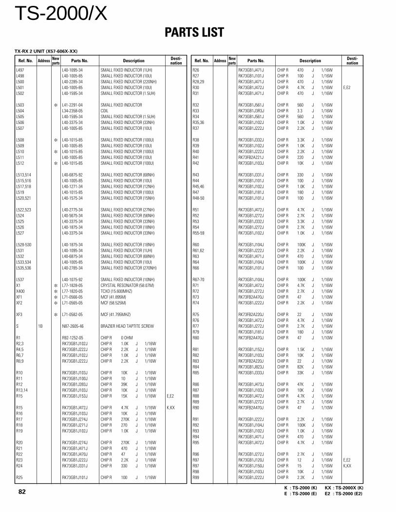
TS-2000/XPARTS LIST
82K : TS-2000 (K) KX : TS-2000X (K)
E : TS-2000 (E) E2 : TS-2000 (E2)
Ref. No. Address Parts No. Description Ref. No. Address Parts No. DescriptionNew Desti-parts nation
New Desti-parts nation
L497 L40-1095-34 SMALL FIXED INDUCTOR (1UH)L498 L40-1005-85 SMALL FIXED INDUCTOR (10U)L500 L40-2285-34 SMALL FIXED INDUCTOR (220NH)L501 L40-1005-85 SMALL FIXED INDUCTOR (10U)L502 L40-1595-34 SMALL FIXED INDUCTOR (1.5UH)
L503 L41-2291-04 SMALL FIXED INDUCTORL504 L34-2358-05 COILL505 L40-1595-34 SMALL FIXED INDUCTOR (1.5UH)L506 L40-3375-34 SMALL FIXED INDUCTOR (33NH)L507 L40-1005-85 SMALL FIXED INDUCTOR (10U)
L508 L40-1015-85 SMALL FIXED INDUCTOR (100U)L509 L40-1005-85 SMALL FIXED INDUCTOR (10U)L510 L40-1015-85 SMALL FIXED INDUCTOR (100U)L511 L40-1005-85 SMALL FIXED INDUCTOR (10U)L512 L40-1015-85 SMALL FIXED INDUCTOR (100U)
L513,514 L40-6875-92 SMALL FIXED INDUCTOR (68NH)L515,516 L40-1005-85 SMALL FIXED INDUCTOR (10U)L517,518 L40-1271-34 SMALL FIXED INDUCTOR (12NH)L519 L40-1015-85 SMALL FIXED INDUCTOR (100U)L520,521 L40-1575-34 SMALL FIXED INDUCTOR (15NH)
L522,523 L40-2775-34 SMALL FIXED INDUCTOR (27NH)L524 L40-5675-34 SMALL FIXED INDUCTOR (56NH)L525 L40-3375-34 SMALL FIXED INDUCTOR (33NH)L526 L40-1875-34 SMALL FIXED INDUCTOR (18NH)L527 L40-3375-34 SMALL FIXED INDUCTOR (33NH)
L528-530 L40-1875-34 SMALL FIXED INDUCTOR (18NH)L531 L40-1095-34 SMALL FIXED INDUCTOR (1UH)L532 L40-6875-34 SMALL FIXED INDUCTOR (68NH)L533,534 L40-1005-85 SMALL FIXED INDUCTOR (10U)L535,536 L40-2785-34 SMALL FIXED INDUCTOR (270NH)
L537 L40-1075-92 SMALL FIXED INDUCTOR (10NH)X1 L77-1828-05 CRYSTAL RESONATOR (58.07M)X400 L77-1820-05 TCXO (15.600MHZ)XF1 L71-0566-05 MCF (41.895M)XF2 L71-0565-05 MCF (58.525M)
XF3 L71-0582-05 MCF (41.795MHZ)
S 1B N87-2605-46 BRAZIER HEAD TAPTITE SCREW
R1 R92-1252-05 CHIP R 0 OHMR2,3 RK73GB1J102J CHIP R 1.0K J 1/16WR4,5 RK73GB1J222J CHIP R 2.2K J 1/16WR6,7 RK73GB1J102J CHIP R 1.0K J 1/16WR8,9 RK73GB1J222J CHIP R 2.2K J 1/16W
R10 RK73GB1J103J CHIP R 10K J 1/16WR11 RK73GB1J100J CHIP R 10 J 1/16WR12 RK73GB1J393J CHIP R 39K J 1/16WR13,14 RK73GB1J103J CHIP R 10K J 1/16WR15 RK73GB1J153J CHIP R 15K J 1/16W E,E2
R15 RK73GB1J472J CHIP R 4.7K J 1/16W K,KXR16 RK73GB1J103J CHIP R 10K J 1/16WR17 RK73GB1J274J CHIP R 270K J 1/16WR18 RK73GB1J271J CHIP R 270 J 1/16WR19 RK73GB1J102J CHIP R 1.0K J 1/16W
R20 RK73GB1J274J CHIP R 270K J 1/16WR21 RK73GB1J471J CHIP R 470 J 1/16WR22 RK73GB1J470J CHIP R 47 J 1/16WR23 RK73GB1J222J CHIP R 2.2K J 1/16WR24 RK73GB1J331J CHIP R 330 J 1/16W
R25 RK73GB1J101J CHIP R 100 J 1/16W
R26 RK73GB1J471J CHIP R 470 J 1/16WR27 RK73GB1J101J CHIP R 100 J 1/16WR28,29 RK73GB1J471J CHIP R 470 J 1/16WR30 RK73GB1J472J CHIP R 4.7K J 1/16W E,E2R31 RK73GB1J471J CHIP R 470 J 1/16W
R32 RK73GB1J561J CHIP R 560 J 1/16WR33 RK73GB1J3R3J CHIP R 3.3 J 1/16WR34 RK73GB1J561J CHIP R 560 J 1/16WR35,36 RK73GB1J102J CHIP R 1.0K J 1/16WR37 RK73GB1J222J CHIP R 2.2K J 1/16W
R38 RK73GB1J332J CHIP R 3.3K J 1/16WR39 RK73GB1J102J CHIP R 1.0K J 1/16WR40 RK73GB1J222J CHIP R 2.2K J 1/16WR41 RK73FB2A221J CHIP R 220 J 1/10WR42 RK73GB1J103J CHIP R 10K J 1/16W
R43 RK73GB1J331J CHIP R 330 J 1/16WR44 RK73GB1J101J CHIP R 100 J 1/16WR45,46 RK73GB1J102J CHIP R 1.0K J 1/16WR47 RK73GB1J181J CHIP R 180 J 1/16WR48-50 RK73GB1J101J CHIP R 100 J 1/16W
R51 RK73GB1J472J CHIP R 4.7K J 1/16WR52 RK73GB1J272J CHIP R 2.7K J 1/16WR53 RK73GB1J332J CHIP R 3.3K J 1/16WR54 RK73GB1J272J CHIP R 2.7K J 1/16WR55-59 RK73GB1J102J CHIP R 1.0K J 1/16W
R60 RK73GB1J104J CHIP R 100K J 1/16WR61,62 RK73GB1J222J CHIP R 2.2K J 1/16WR63 RK73GB1J471J CHIP R 470 J 1/16WR64 RK73GB1J104J CHIP R 100K J 1/16WR66 RK73GB1J101J CHIP R 100 J 1/16W
R67-70 RK73GB1J104J CHIP R 100K J 1/16WR71 RK73GB1J472J CHIP R 4.7K J 1/16WR72 RK73GB1J272J CHIP R 2.7K J 1/16WR73 RK73FB2A470J CHIP R 47 J 1/10WR74 RK73GB1J222J CHIP R 2.2K J 1/16W
R75 RK73FB2A220J CHIP R 22 J 1/10WR76 RK73GB1J472J CHIP R 4.7K J 1/16WR77 RK73GB1J272J CHIP R 2.7K J 1/16WR79 RK73GB1J181J CHIP R 180 J 1/16WR80 RK73FB2A470J CHIP R 47 J 1/10W
R81 RK73GB1J152J CHIP R 1.5K J 1/16WR82 RK73GB1J103J CHIP R 10K J 1/16WR83 RK73FB2A220J CHIP R 22 J 1/10WR84 RK73GB1J823J CHIP R 82K J 1/16WR85 RK73GB1J333J CHIP R 33K J 1/16W
R86 RK73GB1J473J CHIP R 47K J 1/16WR87 RK73GB1J103J CHIP R 10K J 1/16WR88 RK73GB1J472J CHIP R 4.7K J 1/16WR89 RK73GB1J272J CHIP R 2.7K J 1/16WR90 RK73FB2A470J CHIP R 47 J 1/10W
R91 RK73GB1J222J CHIP R 2.2K J 1/16WR92 RK73GB1J104J CHIP R 100K J 1/16WR93 RK73GB1J102J CHIP R 1.0K J 1/16WR94 RK73GB1J471J CHIP R 470 J 1/16WR95 RK73GB1J472J CHIP R 4.7K J 1/16W
R96 RK73GB1J272J CHIP R 2.7K J 1/16WR97 RK73GB1J120J CHIP R 12 J 1/16W E,E2R97 RK73GB1J150J CHIP R 15 J 1/16W K,KXR98 RK73GB1J103J CHIP R 10K J 1/16WR99 RK73GB1J222J CHIP R 2.2K J 1/16W
TX-RX 2 UNIT (X57-606X-XX)

TS-2000/XPARTS LIST
83K : TS-2000 (K) KX : TS-2000X (K)
E : TS-2000 (E) E2 : TS-2000 (E2)
Ref. No. Address Parts No. Description Ref. No. Address Parts No. DescriptionNew Desti-parts nation
New Desti-parts nation
R100 RK73GB1J104J CHIP R 100K J 1/16WR101 RK73FB2A470J CHIP R 47 J 1/10WR102 RK73GB1J222J CHIP R 2.2K J 1/16WR103 RK73FB2A220J CHIP R 22 J 1/10WR104,105 RK73GB1J101J CHIP R 100 J 1/16W
R106 RK73FB2A470J CHIP R 47 J 1/10WR107 RK73GB1J222J CHIP R 2.2K J 1/16WR108 RK73FB2A470J CHIP R 47 J 1/10WR109 RK73GB1J181J CHIP R 180 J 1/16WR110,111 RK73GB1J104J CHIP R 100K J 1/16W
R112,113 RK73GB1J472J CHIP R 4.7K J 1/16WR114 RK73GB1J272J CHIP R 2.7K J 1/16WR115 RK73GB1J104J CHIP R 100K J 1/16WR116,117 R92-1252-05 CHIP R 0 OHMR118 RK73GB1J272J CHIP R 2.7K J 1/16W
R119 R92-1252-05 CHIP R 0 OHMR120,121 RK73GB1J104J CHIP R 100K J 1/16WR124 RK73GB1J102J CHIP R 1.0K J 1/16WR125 RK73GB1J104J CHIP R 100K J 1/16WR126-128 RK73GB1J102J CHIP R 1.0K J 1/16W
R130 RK73GB1J561J CHIP R 560 J 1/16WR131 RK73GB1J102J CHIP R 1.0K J 1/16WR132 RK73GB1J3R3J CHIP R 3.3 J 1/16WR133 RK73GB1J102J CHIP R 1.0K J 1/16WR135,136 RK73GB1J104J CHIP R 100K J 1/16W
R137 RK73GB1J821J CHIP R 820 J 1/16WR139 RK73GB1J104J CHIP R 100K J 1/16WR140 RK73GB1J331J CHIP R 330 J 1/16WR141 RK73GB1J102J CHIP R 1.0K J 1/16WR142,143 RK73GB1J101J CHIP R 100 J 1/16W
R146,147 RK73GB1J222J CHIP R 2.2K J 1/16WR149 RK73GB1J331J CHIP R 330 J 1/16WR150,151 RK73GB1J561J CHIP R 560 J 1/16WR152 RK73GB1J102J CHIP R 1.0K J 1/16WR153 RK73GB1J180J CHIP R 18 J 1/16W
R154 RK73GB1J3R3J CHIP R 3.3 J 1/16WR155 RK73GB1J390J CHIP R 39 J 1/16WR156 RK73GB1J561J CHIP R 560 J 1/16WR157 RK73GB1J331J CHIP R 330 J 1/16WR158 RK73GB1J102J CHIP R 1.0K J 1/16W
R159 RK73GB1J390J CHIP R 39 J 1/16WR160-163 RK73GB1J102J CHIP R 1.0K J 1/16WR164 RK73GB1J470J CHIP R 47 J 1/16WR165 RK73GB1J332J CHIP R 3.3K J 1/16WR166 R92-1252-05 CHIP R 0 OHM
R167 RK73GB1J681J CHIP R 680 J 1/16WR168 RK73GB1J330J CHIP R 33 J 1/16WR169 RK73GB1J181J CHIP R 180 J 1/16WR170 RK73GB1J472J CHIP R 4.7K J 1/16WR171 RK73GB1J272J CHIP R 2.7K J 1/16W
R172 RK73GB1J101J CHIP R 100 J 1/16WR173 RK73GB1J121J CHIP R 120 J 1/16WR174 RK73GB1J270J CHIP R 27 J 1/16WR175 RK73GB1J330J CHIP R 33 J 1/16WR176 RK73GB1J562J CHIP R 5.6K J 1/16W
R177 RK73GB1J182J CHIP R 1.8K J 1/16WR178 RK73GB1J472J CHIP R 4.7K J 1/16WR179 RK73GB1J272J CHIP R 2.7K J 1/16WR180 RK73GB1J562J CHIP R 5.6K J 1/16WR181 RK73GB1J182J CHIP R 1.8K J 1/16W
R185 RK73GB1J102J CHIP R 1.0K J 1/16WR187 RK73GB1J393J CHIP R 39K J 1/16WR188 RK73GB1J104J CHIP R 100K J 1/16WR189 RK73GB1J273J CHIP R 27K J 1/16WR190 RK73GB1J180J CHIP R 18 J 1/16W
R191 RK73GB1J273J CHIP R 27K J 1/16WR192 R92-1252-05 CHIP R 0 OHMR194 RK73GB1J471J CHIP R 470 J 1/16WR195 RK73GB1J823J CHIP R 82K J 1/16WR196 RK73GB1J103J CHIP R 10K J 1/16W
R197-199 RK73GB1J101J CHIP R 100 J 1/16WR200 RK73GB1J182J CHIP R 1.8K J 1/16WR201 RK73GB1J273J CHIP R 27K J 1/16WR202 RK73GB1J471J CHIP R 470 J 1/16WR203 RK73GB1J102J CHIP R 1.0K J 1/16W
R204 RK73GB1J184J CHIP R 180K J 1/16WR205 RK73GB1J102J CHIP R 1.0K J 1/16WR206 RK73GB1J154J CHIP R 150K J 1/16WR207 R92-1252-05 CHIP R 0 OHMR208 RK73GB1J332J CHIP R 3.3K J 1/16W
R209 R92-1252-05 CHIP R 0 OHMR210 RK73GB1J102J CHIP R 1.0K J 1/16WR211 RK73GB1J153J CHIP R 15K J 1/16W E,E2R212 RK73GB1J563J CHIP R 56K J 1/16WR213,214 RK73GB1J222J CHIP R 2.2K J 1/16W
R215 RK73GB1J101J CHIP R 100 J 1/16WR216 RK73GB1J333J CHIP R 33K J 1/16WR217 RK73GB1J103J CHIP R 10K J 1/16WR218 RK73GB1J102J CHIP R 1.0K J 1/16WR219 RK73GB1J101J CHIP R 100 J 1/16W
R220,221 RK73GB1J223J CHIP R 22K J 1/16W E,E2R222 RK73GB1J682J CHIP R 6.8K J 1/16WR223 RK73GB1J100J CHIP R 10 J 1/16WR224 RK73GB1J221J CHIP R 220 J 1/16WR225,226 RK73GB1J223J CHIP R 22K J 1/16W E,E2
R229 RK73GB1J822J CHIP R 8.2K J 1/16WR230 R92-1252-05 CHIP R 0 OHMR231 RK73GB1J331J CHIP R 330 J 1/16WR232 RK73GB1J221J CHIP R 220 J 1/16WR233 RK73GB1J223J CHIP R 22K J 1/16W
R235 RK73GB1J473J CHIP R 47K J 1/16WR236 RK73GB1J153J CHIP R 15K J 1/16W E,E2R237,238 RK73GB1J331J CHIP R 330 J 1/16WR240,241 RK73GB1J330J CHIP R 33 J 1/16WR242 RK73GB1J222J CHIP R 2.2K J 1/16W
R245 RK73GB1J183J CHIP R 18K J 1/16WR246,247 RK73GB1J680J CHIP R 68 J 1/16WR248 RK73GB1J103J CHIP R 10K J 1/16WR250 RK73GB1J271J CHIP R 270 J 1/16WR254 RK73GB1J100J CHIP R 10 J 1/16W
R255 RK73GB1J472J CHIP R 4.7K J 1/16WR256 RK73GB1J180J CHIP R 18 J 1/16WR257 RK73GB1J103J CHIP R 10K J 1/16WR258 RK73GB1J180J CHIP R 18 J 1/16WR259,260 RK73GB1J222J CHIP R 2.2K J 1/16W
R262 RK73GB1J332J CHIP R 3.3K J 1/16WR263 RK73GB1J180J CHIP R 18 J 1/16WR265 RK73GB1J221J CHIP R 220 J 1/16WR266 RK73GB1J223J CHIP R 22K J 1/16WR267 RK73GB1J822J CHIP R 8.2K J 1/16W
TX-RX 2 UNIT (X57-606X-XX)

TS-2000/XPARTS LIST
84K : TS-2000 (K) KX : TS-2000X (K)
E : TS-2000 (E) E2 : TS-2000 (E2)
Ref. No. Address Parts No. Description Ref. No. Address Parts No. DescriptionNew Desti-parts nation
New Desti-parts nation
R268 RK73GB1J274J CHIP R 270K J 1/16WR269 RK73GB1J564J CHIP R 560K J 1/16WR271 RK73GB1J223J CHIP R 22K J 1/16WR272 RK73GB1J104J CHIP R 100K J 1/16WR276 RK73GB1J101J CHIP R 100 J 1/16W
R277 RK73GB1J183J CHIP R 18K J 1/16WR278 RK73GB1J182J CHIP R 1.8K J 1/16WR286 R92-1252-05 CHIP R 0 OHMR287 RK73GB1J563J CHIP R 56K J 1/16WR288 RK73GB1J102J CHIP R 1.0K J 1/16W
R289 RK73GB1J103J CHIP R 10K J 1/16WR291 RK73GB1J471J CHIP R 470 J 1/16WR295 RK73GB1J102J CHIP R 1.0K J 1/16WR296 RK73GB1J471J CHIP R 470 J 1/16WR297,298 RK73GB1J102J CHIP R 1.0K J 1/16W
R300,301 RK73GB1J560J CHIP R 56 J 1/16WR303 RK73GB1J151J CHIP R 150 J 1/16WR304,305 R92-1252-05 CHIP R 0 OHM K,KXR306 RK73GB1J182J CHIP R 1.8K J 1/16WR307,308 RK73GB1J103J CHIP R 10K J 1/16W
R309 RK73GB1J182J CHIP R 1.8K J 1/16WR310 RK73GB1J472J CHIP R 4.7K J 1/16WR311,312 R92-1252-05 CHIP R 0 OHMR313 RK73GB1J103J CHIP R 10K J 1/16WR314,315 RK73GB1J472J CHIP R 4.7K J 1/16W
R316 RK73GB1J103J CHIP R 10K J 1/16WR317 RK73GB1J471J CHIP R 470 J 1/16WR319,320 RK73GB1J331J CHIP R 330 J 1/16WR321 RK73GB1J820J CHIP R 82 J 1/16WR322 RK73GB1J102J CHIP R 1.0K J 1/16W
R323 RK73GB1J331J CHIP R 330 J 1/16WR325-327 RK73GB1J101J CHIP R 100 J 1/16WR328 RK73GB1J102J CHIP R 1.0K J 1/16WR329 RK73GB1J682J CHIP R 6.8K J 1/16WR333 RK73GB1J153J CHIP R 15K J 1/16W
R335 RK73GB1J102J CHIP R 1.0K J 1/16WR336 RK73GB1J470J CHIP R 47 J 1/16WR337 RK73GB1J330J CHIP R 33 J 1/16WR338 RK73GB1J152J CHIP R 1.5K J 1/16WR340 R92-1252-05 CHIP R 0 OHM
R342 RK73GB1J104J CHIP R 100K J 1/16WR343,344 RK73GB1J331J CHIP R 330 J 1/16WR345 RK73GB1J682J CHIP R 6.8K J 1/16WR346,347 RK73GB1J103J CHIP R 10K J 1/16WR348 RK73GB1J182J CHIP R 1.8K J 1/16W
R349 R92-1252-05 CHIP R 0 OHM E,E2R349,350 R92-1252-05 CHIP R 0 OHM K,KXR350 RK73GB1J100J CHIP R 10 J 1/16W E,E2R351 RK73GB1J823J CHIP R 82K J 1/16WR352 RK73GB1J104J CHIP R 100K J 1/16W
R353 RK73GB1J103J CHIP R 10K J 1/16WR354 R92-1252-05 CHIP R 0 OHMR355 RK73GB1J472J CHIP R 4.7K J 1/16WR356 RK73GB1J103J CHIP R 10K J 1/16WR357 RK73GB1J470J CHIP R 47 J 1/16W
R358 R92-1252-05 CHIP R 0 OHMR359 RK73GB1J223J CHIP R 22K J 1/16WR360 RK73GB1J474J CHIP R 470K J 1/16WR361 RK73GB1J272J CHIP R 2.7K J 1/16WR362 R92-1252-05 CHIP R 0 OHM
R363 RK73GB1J153J CHIP R 15K J 1/16WR365 R92-1252-05 CHIP R 0 OHMR366 RK73GB1J221J CHIP R 220 J 1/16WR368 RK73GB1J221J CHIP R 220 J 1/16WR369 RK73FB2A393J CHIP R 39K J 1/10W
R370 RK73GB1J471J CHIP R 470 J 1/16WR371 RK73GB1J822J CHIP R 8.2K J 1/16WR372 RK73GB1J153J CHIP R 15K J 1/16WR373 RK73GB1J391J CHIP R 390 J 1/16WR374-376 RK73GB1J101J CHIP R 100 J 1/16W
R377 RK73GB1J560J CHIP R 56 J 1/16WR378 RK73GB1J224J CHIP R 220K J 1/16WR379 RK73GB1J474J CHIP R 470K J 1/16WR380 RK73GB1J684J CHIP R 680K J 1/16WR381 RK73GB1J104J CHIP R 100K J 1/16W
R382 RK73GB1J474J CHIP R 470K J 1/16WR383 RK73GB1J391J CHIP R 390 J 1/16WR384 R92-1252-05 CHIP R 0 OHMR385-387 R92-0679-05 CHIP R 0 OHMR388,389 R92-0670-05 CHIP R 0 OHM
R390 RK73GB1J102J CHIP R 1.0K J 1/16WR391 R92-0679-05 CHIP R 0 OHMR392 RK73GB1J273J CHIP R 27K J 1/16WR393 R92-1252-05 CHIP R 0 OHMR394 R92-0679-05 CHIP R 0 OHM
R395 R92-0670-05 CHIP R 0 OHMR396-398 R92-1252-05 CHIP R 0 OHMR399 RK73FB2A100J CHIP R 10 J 1/10W E,E2R399 RK73FB2A6R8J CHIP R 6.8 J 1/10W K,KXR400-411 RK73GB1J101J CHIP R 100 J 1/16W
R412-417 R92-1252-05 CHIP R 0 OHMR418 RK73GB1J101J CHIP R 100 J 1/16WR419-421 RK73GB1J102J CHIP R 1.0K J 1/16WR422 RK73GB1J222J CHIP R 2.2K J 1/16WR423 R92-1252-05 CHIP R 0 OHM
R424 RK73GB1J101J CHIP R 100 J 1/16WR427 RK73GB1J101J CHIP R 100 J 1/16WR428-431 RK73GB1J123J CHIP R 12K J 1/16WR432 R92-1252-05 CHIP R 0 OHMR433,434 RK73GB1J473J CHIP R 47K J 1/16W
R435 RK73GB1J474J CHIP R 470K J 1/16WR436 RK73GB1J103J CHIP R 10K J 1/16WR437 RK73GB1J332J CHIP R 3.3K J 1/16WR438 RK73GB1J102J CHIP R 1.0K J 1/16WR439,440 RK73GB1J220J CHIP R 22 J 1/16W
R441 RK73GB1J181J CHIP R 180 J 1/16WR442 RK73GB1J102J CHIP R 1.0K J 1/16WR443,444 RK73GB1J101J CHIP R 100 J 1/16WR445 RK73GB1J682J CHIP R 6.8K J 1/16WR447,448 RK73GB1J101J CHIP R 100 J 1/16W
R449 RK73GB1J103J CHIP R 10K J 1/16WR450 RK73GB1J224J CHIP R 220K J 1/16WR451 RK73GB1J391J CHIP R 390 J 1/16WR452 R92-1252-05 CHIP R 0 OHMR453 RK73GB1J153J CHIP R 15K J 1/16W
R454 RK73GB1J682J CHIP R 6.8K J 1/16WR455 RK73GB1J153J CHIP R 15K J 1/16WR456 RK73GB1J682J CHIP R 6.8K J 1/16WR457 RK73GB1J470J CHIP R 47 J 1/16WR458 RK73GB1J153J CHIP R 15K J 1/16W
TX-RX 2 UNIT (X57-606X-XX)

TS-2000/XPARTS LIST
85K : TS-2000 (K) KX : TS-2000X (K)
E : TS-2000 (E) E2 : TS-2000 (E2)
Ref. No. Address Parts No. Description Ref. No. Address Parts No. DescriptionNew Desti-parts nation
New Desti-parts nation
R459 RK73GB1J682J CHIP R 6.8K J 1/16WR460 RK73GB1J220J CHIP R 22 J 1/16WR461 RK73GB1J181J CHIP R 180 J 1/16WR462 RK73GB1J470J CHIP R 47 J 1/16WR463 RK73GB1J181J CHIP R 180 J 1/16W
R464,465 RK73GB1J101J CHIP R 100 J 1/16WR466 RK73GB1J470J CHIP R 47 J 1/16WR467 RK73GB1J181J CHIP R 180 J 1/16WR468 RK73GB1J470J CHIP R 47 J 1/16WR469 RK73GB1J391J CHIP R 390 J 1/16W
R470 RK73GB1J120J CHIP R 12 J 1/16WR471 R92-1252-05 CHIP R 0 OHMR472 RK73GB1J470J CHIP R 47 J 1/16WR473 RK73GB1J181J CHIP R 180 J 1/16WR474 RK73GB1J391J CHIP R 390 J 1/16W
R475 RK73GB1J181J CHIP R 180 J 1/16WR476 R92-1252-05 CHIP R 0 OHMR477 RK73GB1J153J CHIP R 15K J 1/16WR478 RK73GB1J682J CHIP R 6.8K J 1/16WR479 RK73GB1J681J CHIP R 680 J 1/16W
R480 RK73GB1J101J CHIP R 100 J 1/16WR481-483 R92-1252-05 CHIP R 0 OHMR484 RK73GB1J470J CHIP R 47 J 1/16WR485,486 R92-1252-05 CHIP R 0 OHMR487 RK73GB1J151J CHIP R 150 J 1/16W
R488 RK73GB1J153J CHIP R 15K J 1/16WR489 RK73GB1J682J CHIP R 6.8K J 1/16WR490 R92-1252-05 CHIP R 0 OHMR491 RK73GB1J390J CHIP R 39 J 1/16WR492 R92-1252-05 CHIP R 0 OHM
R493 RK73GB1J151J CHIP R 150 J 1/16WR494 RK73GB1J271J CHIP R 270 J 1/16WR495 RK73GB1J103J CHIP R 10K J 1/16WR496 RK73GB1J472J CHIP R 4.7K J 1/16WR497 RK73GB1J101J CHIP R 100 J 1/16W
R498 RK73GB1J822J CHIP R 8.2K J 1/16WR499 RK73GB1J153J CHIP R 15K J 1/16WR500 RK73GB1J472J CHIP R 4.7K J 1/16WR501 RK73GB1J153J CHIP R 15K J 1/16WR502 RK73GB1J682J CHIP R 6.8K J 1/16W
R503 RK73GB1J181J CHIP R 180 J 1/16WR504 RK73GB1J470J CHIP R 47 J 1/16WR505 RK73GB1J391J CHIP R 390 J 1/16WR506 RK73GB1J821J CHIP R 820 J 1/16WR507 RK73GB1J121J CHIP R 120 J 1/16W
R508 RK73GB1J820J CHIP R 82 J 1/16WR509 RK73GB1J5R6J CHIP R 5.6 J 1/16WR510 RK73GB1J101J CHIP R 100 J 1/16WR511 RK73GB1J821J CHIP R 820 J 1/16WR512 RK73GB1J470J CHIP R 47 J 1/16W
R513 RK73GB1J820J CHIP R 82 J 1/16WR514,515 R92-1252-05 CHIP R 0 OHMR516 RK73GB1J101J CHIP R 100 J 1/16WR517-519 RK73GB1J470J CHIP R 47 J 1/16WR520,521 RK73GB1J823J CHIP R 82K J 1/16W
R522,523 RK73GB1J561J CHIP R 560 J 1/16WR524 RK73GB1J823J CHIP R 82K J 1/16WR525,526 RK73GB1J392J CHIP R 3.9K J 1/16WR527 RK73GB1J561J CHIP R 560 J 1/16WR528 RK73GB1J682J CHIP R 6.8K J 1/16W
R529,530 RK73GB1J101J CHIP R 100 J 1/16WR531 RK73GB1J392J CHIP R 3.9K J 1/16WR532 RK73GB1J470J CHIP R 47 J 1/16WR533 RK73GB1J151J CHIP R 150 J 1/16WR534 RK73GB1J682J CHIP R 6.8K J 1/16W
R535 RK73GB1J470J CHIP R 47 J 1/16WR536 RK73GB1J153J CHIP R 15K J 1/16WR537,538 RK73GB1J331J CHIP R 330 J 1/16WR539 RK73GB1J271J CHIP R 270 J 1/16WR540 RK73GB1J470J CHIP R 47 J 1/16W
R541 RK73GB1J101J CHIP R 100 J 1/16WR542 RK73GB1J822J CHIP R 8.2K J 1/16WR543 RK73GB1J153J CHIP R 15K J 1/16WR544 RK73GB1J101J CHIP R 100 J 1/16WR545 RK73GB1J822J CHIP R 8.2K J 1/16W
R546 RK73GB1J153J CHIP R 15K J 1/16WR547,548 RK73GB1J391J CHIP R 390 J 1/16WR549 RK73GB1J331J CHIP R 330 J 1/16WR550 RK73GB1J221J CHIP R 220 J 1/16WR551 RK73GB1J331J CHIP R 330 J 1/16W
R552 RK73GB1J221J CHIP R 220 J 1/16WR553 RK73GB1J331J CHIP R 330 J 1/16WR554 RK73GB1J101J CHIP R 100 J 1/16WR555 RK73GB1J822J CHIP R 8.2K J 1/16WR556 RK73GB1J153J CHIP R 15K J 1/16W
R557 RK73GB1J101J CHIP R 100 J 1/16WR558 RK73GB1J181J CHIP R 180 J 1/16WR559 RK73GB1J391J CHIP R 390 J 1/16WR560 RK73GB1J153J CHIP R 15K J 1/16WR561 RK73GB1J682J CHIP R 6.8K J 1/16W
R562 RK73GB1J331J CHIP R 330 J 1/16WR563 RK73GB1J221J CHIP R 220 J 1/16WR564 RK73GB1J271J CHIP R 270 J 1/16WR565 RK73GB1J150J CHIP R 15 J 1/16WR566 RK73GB1J221J CHIP R 220 J 1/16W
R567 RK73GB1J470J CHIP R 47 J 1/16WR568 RK73GB1J181J CHIP R 180 J 1/16WR569 RK73GB1J150J CHIP R 15 J 1/16WR570 R92-1252-05 CHIP R 0 OHMR571 RK73GB1J153J CHIP R 15K J 1/16W
R572 RK73GB1J682J CHIP R 6.8K J 1/16WR573 RK73GB1J101J CHIP R 100 J 1/16WR574 RK73GB1J150J CHIP R 15 J 1/16WR575 R92-1252-05 CHIP R 0 OHMR576 RK73GB1J470J CHIP R 47 J 1/16W
R577 RK73GB1J181J CHIP R 180 J 1/16WR578 R92-1252-05 CHIP R 0 OHMR579 RK73GB1J101J CHIP R 100 J 1/16WR580 R92-1252-05 CHIP R 0 OHMR581 RK73GB1J682J CHIP R 6.8K J 1/16W
R583 RK73GB1J101J CHIP R 100 J 1/16WR585 RK73GB1J101J CHIP R 100 J 1/16WR586 RK73GB1J472J CHIP R 4.7K J 1/16WR587 RK73GB1J101J CHIP R 100 J 1/16WR588 RK73GB1J470J CHIP R 47 J 1/16W
R589 RK73GB1J151J CHIP R 150 J 1/16WR593 RK73GB1J682J CHIP R 6.8K J 1/16WR596 RK73GB1J153J CHIP R 15K J 1/16WR598 RK73GB1J271J CHIP R 270 J 1/16WR600 RK73GB1J470J CHIP R 47 J 1/16W
TX-RX 2 UNIT (X57-606X-XX)

TS-2000/XPARTS LIST
86K : TS-2000 (K) KX : TS-2000X (K)
E : TS-2000 (E) E2 : TS-2000 (E2)
Ref. No. Address Parts No. Description Ref. No. Address Parts No. DescriptionNew Desti-parts nation
New Desti-parts nation
R602 RK73GB1J151J CHIP R 150 J 1/16WR603 RK73GB1J390J CHIP R 39 J 1/16WR604-606 RK73GB1J101J CHIP R 100 J 1/16WR607 RK73GB1J182J CHIP R 1.8K J 1/16WR608 RK73GB1J151J CHIP R 150 J 1/16W
R609 RK73GB1J101J CHIP R 100 J 1/16WR610 RK73GB1J182J CHIP R 1.8K J 1/16WR611 RK73GB1J222J CHIP R 2.2K J 1/16WR612 R92-1252-05 CHIP R 0 OHMR613 RK73GB1J150J CHIP R 15 J 1/16W
R614 RK73GB1J222J CHIP R 2.2K J 1/16WR615 R92-1252-05 CHIP R 0 OHMR616 RK73GB1J151J CHIP R 150 J 1/16WR617 RK73GB1J472J CHIP R 4.7K J 1/16WR618 RK73GB1J390J CHIP R 39 J 1/16W
R619,620 RK73GB1J101J CHIP R 100 J 1/16WR621 RK73GB1J150J CHIP R 15 J 1/16WR622 RK73GB1J101J CHIP R 100 J 1/16WR623,624 RK73GB1J151J CHIP R 150 J 1/16WR625 R92-1252-05 CHIP R 0 OHM
R626 RK73GB1J474J CHIP R 470K J 1/16WR627 RK73GB1J150J CHIP R 15 J 1/16WR628 R92-1252-05 CHIP R 0 OHMR629 RK73GB1J474J CHIP R 470K J 1/16WR630 RK73GB1J390J CHIP R 39 J 1/16W
R631 RK73GB1J102J CHIP R 1.0K J 1/16WR632 RK73GB1J151J CHIP R 150 J 1/16WR633,634 RK73GB1J150J CHIP R 15 J 1/16WR635 RK73GB1J681J CHIP R 680 J 1/16WR636 RK73GB1J271J CHIP R 270 J 1/16W
R637,638 RK73GB1J682J CHIP R 6.8K J 1/16WR639 RK73GB1J681J CHIP R 680 J 1/16WR640 RK73GB1J222J CHIP R 2.2K J 1/16WR641 RK73GB1J470J CHIP R 47 J 1/16WR642 RK73GB1J153J CHIP R 15K J 1/16W
R643 RK73GB1J682J CHIP R 6.8K J 1/16WR644 RK73GB1J180J CHIP R 18 J 1/16WR645 RK73GB1J222J CHIP R 2.2K J 1/16WR646 RK73GB1J271J CHIP R 270 J 1/16WR647 RK73GB1J102J CHIP R 1.0K J 1/16W
R648 RK73GB1J471J CHIP R 470 J 1/16WR649 RK73GB1J472J CHIP R 4.7K J 1/16WR650 RK73GB1J102J CHIP R 1.0K J 1/16WR651 RK73GB1J391J CHIP R 390 J 1/16WR652 R92-1252-05 CHIP R 0 OHM
R653 RK73GB1J391J CHIP R 390 J 1/16WR654,655 R92-1252-05 CHIP R 0 OHMR656 RK73GB1J472J CHIP R 4.7K J 1/16WR657 RK73GB1J153J CHIP R 15K J 1/16WR658 RK73GB1J682J CHIP R 6.8K J 1/16W
R659,660 RK73GB1J102J CHIP R 1.0K J 1/16WR661 RK73GB1J150J CHIP R 15 J 1/16WR663 RK73GB1J471J CHIP R 470 J 1/16WR664 RK73GB1J151J CHIP R 150 J 1/16WR665 RK73GB1J102J CHIP R 1.0K J 1/16W
R666 RK73GB1J390J CHIP R 39 J 1/16WR667 RK73GB1J150J CHIP R 15 J 1/16WR668 RK73GB1J101J CHIP R 100 J 1/16WR669 RK73GB1J150J CHIP R 15 J 1/16WR670 RK73GB1J470J CHIP R 47 J 1/16W
R671 RK73GB1J151J CHIP R 150 J 1/16WR675 RK73GB1J391J CHIP R 390 J 1/16WR676 RK73GB1J151J CHIP R 150 J 1/16WR677,678 RK73GB1J101J CHIP R 100 J 1/16WR680 RK73GB1J390J CHIP R 39 J 1/16W
R681-683 R92-1252-05 CHIP R 0 OHMR685 R92-1252-05 CHIP R 0 OHMR686 RK73GB1J151J CHIP R 150 J 1/16WR687 R92-1252-05 CHIP R 0 OHMR689,690 R92-1252-05 CHIP R 0 OHM
R692 RK73GB1J101J CHIP R 100 J 1/16WR693 RK73GB1J102J CHIP R 1.0K J 1/16WR694 RK73GB1J153J CHIP R 15K J 1/16WR695 RK73GB1J682J CHIP R 6.8K J 1/16WR696 RK73GB1J470J CHIP R 47 J 1/16W
R697 RK73GB1J121J CHIP R 120 J 1/16WR698 RK73GB1J682J CHIP R 6.8K J 1/16WR699 RK73GB1J391J CHIP R 390 J 1/16WR700 R92-1252-05 CHIP R 0 OHMR701 RK73GB1J102J CHIP R 1.0K J 1/16W
R702,703 RK73GB1J103J CHIP R 10K J 1/16WR710-713 RK73GB1J472J CHIP R 4.7K J 1/16WR714,715 RK73GB1J101J CHIP R 100 J 1/16WR716-719 RK73GB1J102J CHIP R 1.0K J 1/16WR720 RK73GB1J182J CHIP R 1.8K J 1/16W
R721 R92-1252-05 CHIP R 0 OHMR722,723 RK73GB1J101J CHIP R 100 J 1/16WR724,725 RK73GB1J102J CHIP R 1.0K J 1/16WR726 RK73GB1J101J CHIP R 100 J 1/16WR727 RK73GB1J680J CHIP R 68 J 1/16W
R728-731 RK73GB1J102J CHIP R 1.0K J 1/16WR732,733 R92-1252-05 CHIP R 0 OHMR734 RK73GB1J101J CHIP R 100 J 1/16WR735,736 RK73GB1J391J CHIP R 390 J 1/16WR737 RK73GB1J103J CHIP R 10K J 1/16W
R738 RK73GB1J120J CHIP R 12 J 1/16WR739,740 RK73GB1J472J CHIP R 4.7K J 1/16WR741 RK73GB1J120J CHIP R 12 J 1/16WR742,743 RK73GB1J472J CHIP R 4.7K J 1/16WR744 RK73GB1J271J CHIP R 270 J 1/16W
R745,746 RK73GB1J391J CHIP R 390 J 1/16WR747 RK73GB1J180J CHIP R 18 J 1/16WR749,750 RK73GB1J102J CHIP R 1.0K J 1/16WR751 RK73GB1J271J CHIP R 270 J 1/16WR752 RK73GB1J102J CHIP R 1.0K J 1/16W
R753,754 R92-1252-05 CHIP R 0 OHMR755 RK73GB1J470J CHIP R 47 J 1/16WR756 RK73GB1J153J CHIP R 15K J 1/16WR757 RK73GB1J682J CHIP R 6.8K J 1/16WR758 RK73GB1J102J CHIP R 1.0K J 1/16W
R759 RK73GB1J181J CHIP R 180 J 1/16WR760-762 RK73GB1J102J CHIP R 1.0K J 1/16WR763 RK73GB1J472J CHIP R 4.7K J 1/16WR764,765 RK73GB1J102J CHIP R 1.0K J 1/16WR766 RK73GB1J271J CHIP R 270 J 1/16W
R767 RK73GB1J180J CHIP R 18 J 1/16WR768-770 RK73GB1J271J CHIP R 270 J 1/16WR771,772 RK73GB1J180J CHIP R 18 J 1/16WR773,774 RK73GB1J271J CHIP R 270 J 1/16WR775 R92-1252-05 CHIP R 0 OHM
TX-RX 2 UNIT (X57-606X-XX)

TS-2000/XPARTS LIST
87K : TS-2000 (K) KX : TS-2000X (K)
E : TS-2000 (E) E2 : TS-2000 (E2)
Ref. No. Address Parts No. Description Ref. No. Address Parts No. DescriptionNew Desti-parts nation
New Desti-parts nation
D6,7 RN731V DIODED9-11 HSC277 DIODED12 RN731V DIODED13 HSC277 DIODED14 RN731V DIODE
D15 HSC277 DIODED16 HVC131 DIODED17 HSC277 DIODED18 HVC131 DIODED19 RN731V DIODE
D20 HSC277 DIODED21 RN731V DIODED22-24 HSC277 DIODED30-34 HVC350B VARIABLE CAPACITANCE DIODED36,37 HVC350B VARIABLE CAPACITANCE DIODE
D39-43 HVC350B VARIABLE CAPACITANCE DIODED46 DAN235E DIODED47 HVC350B VARIABLE CAPACITANCE DIODED48,49 HSC277 DIODED51 HVC350B VARIABLE CAPACITANCE DIODE
D52,53 DAN235E DIODED54 HSB88WS DIODED56 DAN235E DIODE K,KXD56,57 DAN235E DIODE E,E2D58 RB706F-40 DIODE
D59 DAN235E DIODE E,E2D63-66 1SS355 DIODED68 DAN222 DIODED69 1SS355 DIODED71 1SS355 DIODE
D73,74 DAN222 DIODED75,76 1SS355 DIODED77,78 MA742 DIODED79,80 HVC350B VARIABLE CAPACITANCE DIODED81,82 HVC131 DIODE
D83 MA742 DIODED84-88 HVC350B VARIABLE CAPACITANCE DIODED89 DTZ3.9(B) ZENER DIODED90,91 HSC277 DIODED92-94 HVC131 DIODE
D95 HSC277 DIODED96,97 HVC131 DIODED98 DAN222 DIODED99 1SS355 DIODED100 HVC350B VARIABLE CAPACITANCE DIODE
D101 HSC277 DIODED400 MA2S111 DIODED401,402 KV1460 VARIABLE CAPACITANCE DIODED403 MA2S304 VARIABLE CAPACITANCE DIODED404,405 MA2S077 DIODE
D406 MA2S304 VARIABLE CAPACITANCE DIODED407 MA2S111 DIODED408 KV1460 VARIABLE CAPACITANCE DIODED409-412 1SV283 VARIABLE CAPACITANCE DIODED413 KV1460 VARIABLE CAPACITANCE DIODE
D416,417 1SV283 VARIABLE CAPACITANCE DIODED418,419 MA2S077 DIODED420 1SV283 VARIABLE CAPACITANCE DIODED421 MA2S077 DIODED422,423 MA2S111 DIODE
D426-429 RN731V DIODED430-437 MA2S077 DIODED438 MA2S111 DIODED439-444 MA2S077 DIODED445-447 MA2S111 DIODE
IC2 BU2099FV ICIC3 UPC1678G ICIC4,5 GN2011(Q) ICIC6 UPB1509GV ICIC7 TA31136FN IC
IC8 TC4W53FU ICIC9 NJM2904V ICIC400 TA7808F ICIC401 LMX2306TMX ICIC402 LMX2316TMX IC
IC403 TA7805F ICIC404 BU4094BCFV ICIC405 UPC2709TB ICIC406-408 AD9835BRU ICIC409-412 LMX2306TMX IC
IC414 LMX2306TMX ICIC415,416 UPC2709TB ICQ1,2 DTC114EUA DIGITAL TRANSISTORQ3 FMA5 TRANSISTORQ11 UMC2N TRANSISTOR
Q13 FMA5 TRANSISTORQ14,15 3SK241(R) FETQ16 UMC2N TRANSISTORQ17,18 2SC3356 TRANSISTORQ19 2SC5066(O) TRANSISTOR
Q20 2SK302(GR) FETQ21,22 2SC3357 TRANSISTORQ23 3SK298 FETQ24,25 2SC3357 TRANSISTORQ26 2SC3356 TRANSISTOR
Q30 2SC3356 TRANSISTORQ31 UMC2N TRANSISTORQ32-34 2SC3356 TRANSISTORQ35 DTA114EUA DIGITAL TRANSISTORQ36 UMC2N TRANSISTOR
Q37 3SK298 FETQ38 3SK131(M) FETQ39 2SC4617(R) TRANSISTORQ40 DTA114EUA DIGITAL TRANSISTOR E,E2Q41 DTC144EUA DIGITAL TRANSISTOR E,E2
Q42,43 2SK520(K43) FETQ44,45 2SC4617(R) TRANSISTORQ46,47 3SK131(M) FETQ48 2SC4617(R) TRANSISTORQ50,51 2SC4617(R) TRANSISTOR
Q55,56 2SB1132(Q,R) TRANSISTORQ57-60 DTC114EUA DIGITAL TRANSISTORQ61 2SC3356 TRANSISTORQ62 2SA1362(Y) TRANSISTORQ63 2SC4617(S) TRANSISTOR
Q65 2SC4617(R) TRANSISTORQ66 FMA1A TRANSISTORQ67 DTA114EUA DIGITAL TRANSISTORQ400-402 2SC3722K(R) TRANSISTORQ403-405 DTC114EUA DIGITAL TRANSISTOR
TX-RX 2 UNIT (X57-606X-XX)
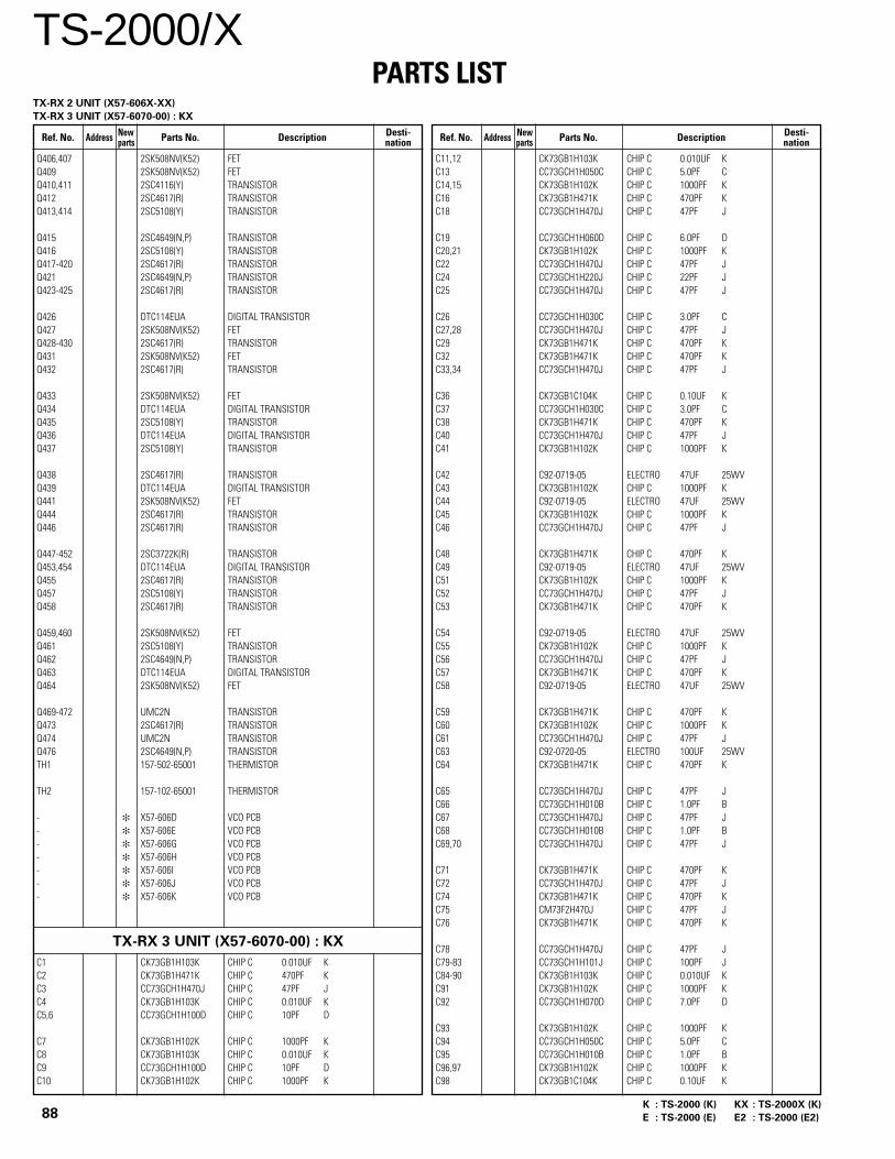
TS-2000/XPARTS LIST
88K : TS-2000 (K) KX : TS-2000X (K)
E : TS-2000 (E) E2 : TS-2000 (E2)
Ref. No. Address Parts No. Description Ref. No. Address Parts No. DescriptionNew Desti-parts nation
New Desti-parts nation
Q406,407 2SK508NV(K52) FETQ409 2SK508NV(K52) FETQ410,411 2SC4116(Y) TRANSISTORQ412 2SC4617(R) TRANSISTORQ413,414 2SC5108(Y) TRANSISTOR
Q415 2SC4649(N,P) TRANSISTORQ416 2SC5108(Y) TRANSISTORQ417-420 2SC4617(R) TRANSISTORQ421 2SC4649(N,P) TRANSISTORQ423-425 2SC4617(R) TRANSISTOR
Q426 DTC114EUA DIGITAL TRANSISTORQ427 2SK508NV(K52) FETQ428-430 2SC4617(R) TRANSISTORQ431 2SK508NV(K52) FETQ432 2SC4617(R) TRANSISTOR
Q433 2SK508NV(K52) FETQ434 DTC114EUA DIGITAL TRANSISTORQ435 2SC5108(Y) TRANSISTORQ436 DTC114EUA DIGITAL TRANSISTORQ437 2SC5108(Y) TRANSISTOR
Q438 2SC4617(R) TRANSISTORQ439 DTC114EUA DIGITAL TRANSISTORQ441 2SK508NV(K52) FETQ444 2SC4617(R) TRANSISTORQ446 2SC4617(R) TRANSISTOR
Q447-452 2SC3722K(R) TRANSISTORQ453,454 DTC114EUA DIGITAL TRANSISTORQ455 2SC4617(R) TRANSISTORQ457 2SC5108(Y) TRANSISTORQ458 2SC4617(R) TRANSISTOR
Q459,460 2SK508NV(K52) FETQ461 2SC5108(Y) TRANSISTORQ462 2SC4649(N,P) TRANSISTORQ463 DTC114EUA DIGITAL TRANSISTORQ464 2SK508NV(K52) FET
Q469-472 UMC2N TRANSISTORQ473 2SC4617(R) TRANSISTORQ474 UMC2N TRANSISTORQ476 2SC4649(N,P) TRANSISTORTH1 157-502-65001 THERMISTOR
TH2 157-102-65001 THERMISTOR
- X57-606D VCO PCB- X57-606E VCO PCB- X57-606G VCO PCB- X57-606H VCO PCB- X57-606I VCO PCB- X57-606J VCO PCB- X57-606K VCO PCB
C1 CK73GB1H103K CHIP C 0.010UF KC2 CK73GB1H471K CHIP C 470PF KC3 CC73GCH1H470J CHIP C 47PF JC4 CK73GB1H103K CHIP C 0.010UF KC5,6 CC73GCH1H100D CHIP C 10PF D
C7 CK73GB1H102K CHIP C 1000PF KC8 CK73GB1H103K CHIP C 0.010UF KC9 CC73GCH1H100D CHIP C 10PF DC10 CK73GB1H102K CHIP C 1000PF K
C11,12 CK73GB1H103K CHIP C 0.010UF KC13 CC73GCH1H050C CHIP C 5.0PF CC14,15 CK73GB1H102K CHIP C 1000PF KC16 CK73GB1H471K CHIP C 470PF KC18 CC73GCH1H470J CHIP C 47PF J
C19 CC73GCH1H060D CHIP C 6.0PF DC20,21 CK73GB1H102K CHIP C 1000PF KC22 CC73GCH1H470J CHIP C 47PF JC24 CC73GCH1H220J CHIP C 22PF JC25 CC73GCH1H470J CHIP C 47PF J
C26 CC73GCH1H030C CHIP C 3.0PF CC27,28 CC73GCH1H470J CHIP C 47PF JC29 CK73GB1H471K CHIP C 470PF KC32 CK73GB1H471K CHIP C 470PF KC33,34 CC73GCH1H470J CHIP C 47PF J
C36 CK73GB1C104K CHIP C 0.10UF KC37 CC73GCH1H030C CHIP C 3.0PF CC38 CK73GB1H471K CHIP C 470PF KC40 CC73GCH1H470J CHIP C 47PF JC41 CK73GB1H102K CHIP C 1000PF K
C42 C92-0719-05 ELECTRO 47UF 25WVC43 CK73GB1H102K CHIP C 1000PF KC44 C92-0719-05 ELECTRO 47UF 25WVC45 CK73GB1H102K CHIP C 1000PF KC46 CC73GCH1H470J CHIP C 47PF J
C48 CK73GB1H471K CHIP C 470PF KC49 C92-0719-05 ELECTRO 47UF 25WVC51 CK73GB1H102K CHIP C 1000PF KC52 CC73GCH1H470J CHIP C 47PF JC53 CK73GB1H471K CHIP C 470PF K
C54 C92-0719-05 ELECTRO 47UF 25WVC55 CK73GB1H102K CHIP C 1000PF KC56 CC73GCH1H470J CHIP C 47PF JC57 CK73GB1H471K CHIP C 470PF KC58 C92-0719-05 ELECTRO 47UF 25WV
C59 CK73GB1H471K CHIP C 470PF KC60 CK73GB1H102K CHIP C 1000PF KC61 CC73GCH1H470J CHIP C 47PF JC63 C92-0720-05 ELECTRO 100UF 25WVC64 CK73GB1H471K CHIP C 470PF K
C65 CC73GCH1H470J CHIP C 47PF JC66 CC73GCH1H010B CHIP C 1.0PF BC67 CC73GCH1H470J CHIP C 47PF JC68 CC73GCH1H010B CHIP C 1.0PF BC69,70 CC73GCH1H470J CHIP C 47PF J
C71 CK73GB1H471K CHIP C 470PF KC72 CC73GCH1H470J CHIP C 47PF JC74 CK73GB1H471K CHIP C 470PF KC75 CM73F2H470J CHIP C 47PF JC76 CK73GB1H471K CHIP C 470PF K
C78 CC73GCH1H470J CHIP C 47PF JC79-83 CC73GCH1H101J CHIP C 100PF JC84-90 CK73GB1H103K CHIP C 0.010UF KC91 CK73GB1H102K CHIP C 1000PF KC92 CC73GCH1H070D CHIP C 7.0PF D
C93 CK73GB1H102K CHIP C 1000PF KC94 CC73GCH1H050C CHIP C 5.0PF CC95 CC73GCH1H010B CHIP C 1.0PF BC96,97 CK73GB1H102K CHIP C 1000PF KC98 CK73GB1C104K CHIP C 0.10UF K
TX-RX 3 UNIT (X57-6070-00) : KX
TX-RX 2 UNIT (X57-606X-XX)
TX-RX 3 UNIT (X57-6070-00) : KX

TS-2000/XPARTS LIST
89K : TS-2000 (K) KX : TS-2000X (K)
E : TS-2000 (E) E2 : TS-2000 (E2)
Ref. No. Address Parts No. Description Ref. No. Address Parts No. DescriptionNew Desti-parts nation
New Desti-parts nation
C99 CK73GB1H102K CHIP C 1000PF KC101 CC73GCH1H020B CHIP C 2.0PF BC103 CC73GCH1H010B CHIP C 1.0PF BC104 CK73GB1H471K CHIP C 470PF KC105 CC73GCH1H470J CHIP C 47PF J
C106 CC73GCH1H060D CHIP C 6.0PF DC107 CC73GCH1H470J CHIP C 47PF JC108 CK73GB1H471K CHIP C 470PF KC109 CC73GCH1H100D CHIP C 10PF DC110 CC73GCH1HR75B CHIP C 0.75PF B
C111 CK73GB1H471K CHIP C 470PF KC112 CC73GCH1H101J CHIP C 100PF JC113 CC73GCH1H020B CHIP C 2.0PF BC114 CC73GCH1H220J CHIP C 22PF JC116 CC73GCH1H040C CHIP C 4.0PF C
C117 CC73GCH1H470J CHIP C 47PF JC118 CC73GCH1H101J CHIP C 100PF JC119 CK73GB1H103K CHIP C 0.010UF KC120 CC73GCH1H470J CHIP C 47PF JC121,122 CK73GB1H471K CHIP C 470PF K
C123 CC73GCH1H470J CHIP C 47PF JC124 CC73GCH1H101J CHIP C 100PF JC125 CC73GCH1H1R5B CHIP C 1.5PF BC126 CC73GCH1H080D CHIP C 8.0PF DC127 CC73GCH1H010B CHIP C 1.0PF B
C128 CC73GCH1H1R5B CHIP C 1.5PF BC131-134 CC73GCH1H101J CHIP C 100PF JC135 CC73GCH1H470J CHIP C 47PF JC136 CK73GB1H103K CHIP C 0.010UF KC137 C92-0505-05 CHIP-TAN 10UF 16WV
C138 CK73GB1H103K CHIP C 0.010UF KC139,140 CK73GB1H102K CHIP C 1000PF KC142 CC73GCH1H070D CHIP C 7.0PF DC143 CK73GB1H102K CHIP C 1000PF KC144 CC73GCH1H0R3B CHIP C 0.3PF B
C145 CC73GCH1H070D CHIP C 7.0PF DC147 C92-0505-05 CHIP-TAN 10UF 16WVC148 CK73GB1H103K CHIP C 0.010UF KC149 CK73GB1H102K CHIP C 1000PF KC150 CC73GCH1H470J CHIP C 47PF J
C151 CK73GB1H103K CHIP C 0.010UF KC152 CK73GB1H102K CHIP C 1000PF KC153 CC73GCH1H070D CHIP C 7.0PF DC154 CK73GB1H102K CHIP C 1000PF KC155,156 CK73GB1H103K CHIP C 0.010UF K
C158 CC73GCH1H470J CHIP C 47PF JC165 C92-0523-05 CHIP-ELE 10UF 16WVC167 CK73GB1H102K CHIP C 1000PF KC169 CK73GB1H471K CHIP C 470PF KC170,171 CK73GB1H102K CHIP C 1000PF K
C172 CK73GB1H103K CHIP C 0.010UF KC173 CK73GB1H102K CHIP C 1000PF KC174 CK73GB1H471K CHIP C 470PF KC176 C92-0719-05 ELECTRO 47UF 25WVC178 CK73GB1H102K CHIP C 1000PF K
C179 C92-0523-05 CHIP-ELE 10UF 16WVC180 CK73GB1H102K CHIP C 1000PF KC182 CC73GCH1H470J CHIP C 47PF JC183 CK73GB1H471K CHIP C 470PF KC184,185 CC73GCH1H470J CHIP C 47PF J
C186 CK73GB1H471K CHIP C 470PF KC188 CC73GCH1H040C CHIP C 4.0PF CC189 CC73GCH1H220J CHIP C 22PF JC190 CC73GCH1H470J CHIP C 47PF JC191 CC73GCH1H050C CHIP C 5.0PF C
C192 CK73GB1H471K CHIP C 470PF KC193 CC73GCH1H100D CHIP C 10PF DC194 CK73GB1H103K CHIP C 0.010UF KC195 CC73GCH1H101J CHIP C 100PF JC301 CK73GB1H471K CHIP C 470PF K
C302,303 CC73GCH1H101J CHIP C 100PF JC304 CC73GCH1H150J CHIP C 15PF JC305 CK73GB1H102K CHIP C 1000PF KC306 CC73GCH1H150J CHIP C 15PF JC307 CC73GCH1H1R5B CHIP C 1.5PF B
C308 CK73GB1H471K CHIP C 470PF KC309 CC73GCH1H060D CHIP C 6.0PF DC310 CC73GCH1H101J CHIP C 100PF JC311 CC73GCH1H080D CHIP C 8.0PF DC312 CC73GCH1H020B CHIP C 2.0PF B
C313 CC73GCH1H030C CHIP C 3.0PF CC314 CC73GCH1H101J CHIP C 100PF JC315 CC73GCH1H470J CHIP C 47PF JC316 CC73GCH1H030C CHIP C 3.0PF CC317,318 CC73GCH1H010B CHIP C 1.0PF B
C319 CC73GCH1H470J CHIP C 47PF JC320 C92-0717-05 ELECTRO 330UF 16WVC323 CC73GCH1H470J CHIP C 47PF JC326,327 CC73GCH1H470J CHIP C 47PF JC328,329 CK73GB1H103K CHIP C 0.010UF K
C332 CK73GB1C473K CHIP C 0.047UF KC333,334 C92-0543-05 CHIP-TAN 3.3UF 10WVC335 C92-0503-05 CHIP-TAN 0.068UF 35WVC336 CK73GB1H182K CHIP C 1800PF KC367 CC73GCH1H101J CHIP C 100PF J
C368,369 CC73GCH1H020B CHIP C 2.0PF BC370-374 CK73GB1H103K CHIP C 0.010UF KC375,376 CC73GCH1H560J CHIP C 56PF JC377-379 CK73GB1H103K CHIP C 0.010UF KC381,382 CK73GB1H103K CHIP C 0.010UF K
C383 CC73GCH1H080D CHIP C 8.0PF DC384-386 CK73GB1H103K CHIP C 0.010UF KC387 CK73GB1C104K CHIP C 0.10UF KC388 CC73GCH1H330J CHIP C 33PF JC389 CC73GCH1H050C CHIP C 5.0PF C
C390-393 CK73GB1H103K CHIP C 0.010UF KC394 CC73GCH1H010B CHIP C 1.0PF BC395,396 CC73GCH1H180J CHIP C 18PF JC397 CK73GB1H103K CHIP C 0.010UF KC398 CC73GCH1H330J CHIP C 33PF J
C399-401 CK73GB1H103K CHIP C 0.010UF KC402 CC73GCH1H010B CHIP C 1.0PF BC403 CC73GCH1H030C CHIP C 3.0PF CC404 CK73GB1H102K CHIP C 1000PF KTC301 C05-0393-05 CERAMIC TRIMMER CAP (8P)
501 3B E30-3457-05 ANTENNA CABLE- E37-0894-05 LEAD WIRE WITH TERMINAL (+B)- E37-0895-05 LEAD WIRE WITH TERMINAL (GND)504 3C E37-0943-05 LEAD WIRE WITH MINIPIN PLUGCN1 E40-3237-05 PIN ASSY
TX-RX 3 UNIT (X57-6070-00) : KX

TS-2000/XPARTS LIST
90K : TS-2000 (K) KX : TS-2000X (K)
E : TS-2000 (E) E2 : TS-2000 (E2)
Ref. No. Address Parts No. Description Ref. No. Address Parts No. DescriptionNew Desti-parts nation
New Desti-parts nation
CN5 E40-3239-05 PIN ASSYCN6 E40-5978-05 FLAT CABLE CONNECTORCN7,8 E04-0428-05 PIN SOCKETCN9 E04-0190-05 PIN SOCKETCN11-16 E04-0428-05 PIN SOCKET
- F10-2367-04 SHIELDING COVER506 3C F10-2368-03 SHIELDING PLATE- F10-2390-04 SHIELDING CASE- F10-2391-04 SHIELDING CASE- F10-2394-04 SHIELDING CASE
- F10-2396-03 SHIELDING COVER
511 3C G10-1218-04 FIBROUS SHEET
512 3B J21-8401-04 HARDWARE FIXTURE
CF1,2 L72-0343-05 CERAMIC FILTERL1 L92-0158-05 FERRITE CHIPL2 L34-4411-05 COILL3 L34-4651-05 COILL4 L40-1005-85 SMALL FIXED INDUCTOR (10U)
L5 L34-4651-05 COILL7,8 L39-1446-05 TOROIDAL COILL9 L34-4644-05 COILL10 L79-1766-05 DIELECTRIC FILTERL11 L40-1075-92 SMALL FIXED INDUCTOR (10NH)
L12 L79-1766-05 DIELECTRIC FILTERL13 L92-0158-05 FERRITE CHIPL17-19 L92-0158-05 FERRITE CHIPL20,21 L92-0403-05 FERRITE CHIPL22 L34-4411-05 COIL
L23 L40-1005-85 SMALL FIXED INDUCTOR (10U)L24 L34-4644-05 COILL25 L34-4651-05 COILL26-28 L34-4642-05 COILL29 L34-4644-05 COIL
L30 L79-1133-05 DIELECTRIC FILTERL31 L40-8265-92 SMALL FIXED INDUCTOR (8.2NH)L32 L40-6865-92 SMALL FIXED INDUCTOR (6.8NH)L33 L79-1765-05 DIELECTRIC FILTERL34 L40-1075-92 SMALL FIXED INDUCTOR (10NH)
L35 L40-5663-92 SMALL FIXED INDUCTOR (5.6NH)L36 L40-2263-92 SMALL FIXED INDUCTOR (2.2NH)L37 L40-6865-92 SMALL FIXED INDUCTOR (6.8NH)L38 L40-5663-92 SMALL FIXED INDUCTOR (5.6NH)L39 L40-1085-85 SMALL FIXED INDUCTOR (0.10U)
L40,41 L40-1005-85 SMALL FIXED INDUCTOR (10U)L42,43 L34-4644-05 COILL44 L40-1005-85 SMALL FIXED INDUCTOR (10U)L45 L34-4644-05 COILL49-51 L40-1005-85 SMALL FIXED INDUCTOR (10U)
L52 L79-1753-05 DIELECTRIC FILTERL301 L40-1085-92 SMALL FIXED INDUCTOR (100NH)L302 L40-1278-60 SMALL FIXED INDUCTOR (12NH)L303,304 L40-1085-92 SMALL FIXED INDUCTOR (100NH)L305,306 L40-2275-92 SMALL FIXED INDUCTOR (22NH)
L307,308 L40-8265-92 SMALL FIXED INDUCTOR (8.2NH)L309 L40-2275-92 SMALL FIXED INDUCTOR (22NH)L310 L40-5663-92 SMALL FIXED INDUCTOR (5.6NH)L312 L40-4763-92 SMALL FIXED INDUCTOR (4.7NH)L315 L40-4763-92 SMALL FIXED INDUCTOR (4.7NH)
L318,319 L40-2275-92 SMALL FIXED INDUCTOR (22NH)L320,321 L34-4642-05 COILL322 L40-1875-92 SMALL FIXED INDUCTOR (18NH)L323 L40-1595-85 SMALL FIXED INDUCTOR (1.5U)L332 L92-0158-05 FERRITE CHIP
L333 L92-0403-05 FERRITE CHIPL336 L40-2285-92 SMALL FIXED INDUCTOR (220NH)L337 L40-5663-92 SMALL FIXED INDUCTOR (5.6NH)L338 L34-4401-05 COILL339 L34-4026-15 COIL
L340-342 L34-4657-05 COILL343 L40-1005-34 SMALL FIXED INDUCTOR (10UH)L344 L40-4705-85 SMALL FIXED INDUCTOR (47U)L345 L40-1005-34 SMALL FIXED INDUCTOR (10UH)L346 L40-1085-92 SMALL FIXED INDUCTOR (100NH)
L347 L40-4763-92 SMALL FIXED INDUCTOR (4.7NH)L348 L40-5663-92 SMALL FIXED INDUCTOR (5.6NH)XF1 L71-0575-05 MCFXF2 L71-0576-05 MCF
P 3C N30-2606-46 PAN HEAD MACHINE SCREW- N67-2608-46 PAN HEAD SEMS SCREW W (IC2, 3)R 3C N87-2606-46 BRAZIER HEAD TAPTITE SCREW
CP1,2 RK75GB1J101J CHIP-COM 100 J 1/16WR2,3 RK73GB1J102J CHIP R 1.0K J 1/16WR4 RK73GB1J103J CHIP R 10K J 1/16WR5 RK73GB1J273J CHIP R 27K J 1/16WR6 RK73GB1J100J CHIP R 10 J 1/16W
R7 RK73GB1J102J CHIP R 1.0K J 1/16WR8,9 RK73GB1J680J CHIP R 68 J 1/16WR10 RK73GB1J103J CHIP R 10K J 1/16WR11 RK73GB1J273J CHIP R 27K J 1/16WR12,13 RK73GB1J330J CHIP R 33 J 1/16W
R14,15 RK73GB1J331J CHIP R 330 J 1/16WR16 RK73GB1J101J CHIP R 100 J 1/16WR17 RK73GB1J271J CHIP R 270 J 1/16WR18 RK73GB1J180J CHIP R 18 J 1/16WR19 RK73GB1J271J CHIP R 270 J 1/16W
R20 RK73GB1J471J CHIP R 470 J 1/16WR21 RK73GB1J271J CHIP R 270 J 1/16WR22 RK73GB1J272J CHIP R 2.7K J 1/16WR23 RK73GB1J180J CHIP R 18 J 1/16WR24 RK73GB1J472J CHIP R 4.7K J 1/16W
R25 RK73GB1J271J CHIP R 270 J 1/16WR26 RK73GB1J330J CHIP R 33 J 1/16WR27 RK73GB1J222J CHIP R 2.2K J 1/16WR28 RK73GB1J101J CHIP R 100 J 1/16WR29 RK73GB1J151J CHIP R 150 J 1/16W
R30 RK73GB1J390J CHIP R 39 J 1/16WR31 RK73GB1J151J CHIP R 150 J 1/16WR32 RK73GB1J101J CHIP R 100 J 1/16WR34 R92-1252-05 CHIP R 0 OHMR35 RK73GB1J680J CHIP R 68 J 1/16W
R36 RK73GB1J121J CHIP R 120 J 1/16WR37 RK73GB1J152J CHIP R 1.5K J 1/16WR38,39 RK73GB1J470J CHIP R 47 J 1/16WR40 RK73GB1J271J CHIP R 270 J 1/16WR41 RK73GB1J180J CHIP R 18 J 1/16W
R42 RK73GB1J271J CHIP R 270 J 1/16WR43 R92-1259-05 CHIP R 18 J 1/2W
TX-RX 3 UNIT (X57-6070-00) : KX
TS-2000/XPARTS LIST
91K : TS-2000 (K) KX : TS-2000X (K)
E : TS-2000 (E) E2 : TS-2000 (E2)
Ref. No. Address Parts No. Description Ref. No. Address Parts No. DescriptionNew Desti-parts nation
New Desti-parts nation
R44 RK73EB2B560J CHIP R 56 J 1/8WR45 RK73GB1J182J CHIP R 1.8K J 1/16WR46 RK73GB1J103J CHIP R 10K J 1/16WR47 RK73GB1J182J CHIP R 1.8K J 1/16WR48 RK73GB1J103J CHIP R 10K J 1/16W
R49 RK73EB2B560J CHIP R 56 J 1/8WR50 R92-0700-05 CHIP R 180 J 1/2WR51 RK73GB1J101J CHIP R 100 J 1/16WR52 RK73GB1J821J CHIP R 820 J 1/16WR53 RK73GB1J332J CHIP R 3.3K J 1/16W
R54 RK73GB1J101J CHIP R 100 J 1/16WR55 RK73GB1J682J CHIP R 6.8K J 1/16WR56 RK73GB1J680J CHIP R 68 J 1/16WR57,58 RK73GB1J222J CHIP R 2.2K J 1/16WR59 R92-1252-05 CHIP R 0 OHM
R60 RK73GB1J332J CHIP R 3.3K J 1/16WR61 R92-1252-05 CHIP R 0 OHMR62,63 RK73GB1J102J CHIP R 1.0K J 1/16WR64 RK73GB1J101J CHIP R 100 J 1/16WR65 RK73GB1J471J CHIP R 470 J 1/16W
R66 RK73GB1J474J CHIP R 470K J 1/16WR67 RK73GB1J823J CHIP R 82K J 1/16WR68 RK73GB1J273J CHIP R 27K J 1/16WR70 RK73GB1J101J CHIP R 100 J 1/16WR71 RK73GB1J471J CHIP R 470 J 1/16W
R72 RK73GB1J271J CHIP R 270 J 1/16WR73 RK73GB1J100J CHIP R 10 J 1/16WR74 RK73GB1J180J CHIP R 18 J 1/16WR75 RK73GB1J271J CHIP R 270 J 1/16WR76,77 RK73GB1J221J CHIP R 220 J 1/16W
R78 RK73GB1J333J CHIP R 33K J 1/16WR79,80 RK73GB1J473J CHIP R 47K J 1/16WR81 RK73GB1J101J CHIP R 100 J 1/16WR82 RK73GB1J820J CHIP R 82 J 1/16WR83 RK73GB1J470J CHIP R 47 J 1/16W
R85 RK73GB1J330J CHIP R 33 J 1/16WR86 RK73GB1J473J CHIP R 47K J 1/16WR87 RK73GB1J102J CHIP R 1.0K J 1/16WR88 RK73GB1J101J CHIP R 100 J 1/16WR89 RK73GB1J102J CHIP R 1.0K J 1/16W
R90 RK73GB1J470J CHIP R 47 J 1/16WR91 RK73GB1J103J CHIP R 10K J 1/16WR92 RK73GB1J472J CHIP R 4.7K J 1/16WR93 RK73GB1J823J CHIP R 82K J 1/16WR94 RK73GB1J471J CHIP R 470 J 1/16W
R95 RK73GB1J561J CHIP R 560 J 1/16WR96 RK73GB1J101J CHIP R 100 J 1/16WR97 RK73GB1J270J CHIP R 27 J 1/16WR98 RK73GB1J560J CHIP R 56 J 1/16WR99 RK73GB1J332J CHIP R 3.3K J 1/16W
R100 RK73GB1J152J CHIP R 1.5K J 1/16WR101 RK73GB1J822J CHIP R 8.2K J 1/16WR102 RK73GB1J153J CHIP R 15K J 1/16WR103 RK73GB1J471J CHIP R 470 J 1/16WR104,105 RK73GB1J101J CHIP R 100 J 1/16W
R106 RK73GB1J331J CHIP R 330 J 1/16WR108 RK73GB1J102J CHIP R 1.0K J 1/16WR111 RK73GB1J103J CHIP R 10K J 1/16WR112 RK73GB1J222J CHIP R 2.2K J 1/16WR117 RK73GB1J271J CHIP R 270 J 1/16W
R118 RK73GB1J180J CHIP R 18 J 1/16WR119,120 RK73GB1J271J CHIP R 270 J 1/16WR121 RK73GB1J180J CHIP R 18 J 1/16WR122 RK73GB1J271J CHIP R 270 J 1/16WR123 RK73GB1J273J CHIP R 27K J 1/16W
R124 RK73GB1J103J CHIP R 10K J 1/16WR125 RK73GB1J470J CHIP R 47 J 1/16WR126 RK73GB1J101J CHIP R 100 J 1/16WR127 R92-1252-05 CHIP R 0 OHMR130 RK73GB1J472J CHIP R 4.7K J 1/16W
R131 RK73GB1J182J CHIP R 1.8K J 1/16WR132 RK73GB1J180J CHIP R 18 J 1/16WR133 RK73GB1J470J CHIP R 47 J 1/16WR134 RK73GB1J561J CHIP R 560 J 1/16WR135 RK73GB1J560J CHIP R 56 J 1/16W
R301 RK73GB1J471J CHIP R 470 J 1/16WR302 RK73GB1J470J CHIP R 47 J 1/16WR303 RK73GB1J121J CHIP R 120 J 1/16WR304 RK73GB1J100J CHIP R 10 J 1/16WR305 RK73GB1J103J CHIP R 10K J 1/16W
R306 RK73GB1J332J CHIP R 3.3K J 1/16WR307 RK73GB1J470J CHIP R 47 J 1/16WR309,310 R92-1252-05 CHIP R 0 OHMR311 RK73GB1J331J CHIP R 330 J 1/16WR312 RK73GB1J823J CHIP R 82K J 1/16W
R314,315 R92-1252-05 CHIP R 0 OHMR318 RK73GB1J102J CHIP R 1.0K J 1/16WR319 RK73GB1J823J CHIP R 82K J 1/16WR321 RK73GB1J101J CHIP R 100 J 1/16WR322 RK73GB1J821J CHIP R 820 J 1/16W
R323 RK73GB1J220J CHIP R 22 J 1/16WR324 RK73GB1J101J CHIP R 100 J 1/16WR325 RK73GB1J182J CHIP R 1.8K J 1/16WR326 RK73GB1J222J CHIP R 2.2K J 1/16WR327,328 R92-1252-05 CHIP R 0 OHM
R329 RK73GB1J474J CHIP R 470K J 1/16WR330 RK73GB1J222J CHIP R 2.2K J 1/16WR331 RK73GB1J103J CHIP R 10K J 1/16WR332 R92-1252-05 CHIP R 0 OHMR333 RK73GB1J103J CHIP R 10K J 1/16W
R334 RK73GB1J392J CHIP R 3.9K J 1/16WR335 R92-1252-05 CHIP R 0 OHMR342 R92-1252-05 CHIP R 0 OHMR343 RK73GB1J331J CHIP R 330 J 1/16WR351 R92-1252-05 CHIP R 0 OHM
R359 RK73GB1J101J CHIP R 100 J 1/16WR360 RK73GB1J153J CHIP R 15K J 1/16WR361 RK73GB1J682J CHIP R 6.8K J 1/16WR362 RK73GB1J101J CHIP R 100 J 1/16WR363 RK73GB1J151J CHIP R 150 J 1/16W
R364 RK73GB1J101J CHIP R 100 J 1/16WR365 RK73GB1J223J CHIP R 22K J 1/16WR366 RK73GB1J822J CHIP R 8.2K J 1/16WR367 RK73GB1J221J CHIP R 220 J 1/16WR368 R92-1252-05 CHIP R 0 OHM
R369 RK73GB1J330J CHIP R 33 J 1/16WR370 RK73GB1J183J CHIP R 18K J 1/16WR371-373 RK73GB1J330J CHIP R 33 J 1/16WR374 RK73GB1J103J CHIP R 10K J 1/16WR375 RK73GB1J101J CHIP R 100 J 1/16W
TX-RX 3 UNIT (X57-6070-00) : KX

TS-2000/XPARTS LIST
92K : TS-2000 (K) KX : TS-2000X (K)
E : TS-2000 (E) E2 : TS-2000 (E2)
Ref. No. Address Parts No. Description Ref. No. Address Parts No. DescriptionNew Desti-parts nation
New Desti-parts nation
R376 RK73GB1J153J CHIP R 15K J 1/16WR377 RK73GB1J682J CHIP R 6.8K J 1/16WR378 RK73GB1J151J CHIP R 150 J 1/16WR379 RK73GB1J101J CHIP R 100 J 1/16WR381 R92-1252-05 CHIP R 0 OHM
R383 RK73GB1J102J CHIP R 1.0K J 1/16WR384 RK73GB1J470J CHIP R 47 J 1/16WR385,386 RK73GB1J103J CHIP R 10K J 1/16WVR1 R12-6715-05 TRIMMING POT. (22K)VR2 R12-6707-05 TRIMMING POT. (1.0K)
D1 HSB88WS DIODED2 1SS355 DIODED3,4 HSM88ASR DIODED5-7 XB15A709 DIODED8 DAN235E DIODE
D9 1SS355 DIODED10,11 RN731V DIODED12 DAN202K DIODED301 1SV283 VARIABLE CAPACITANCE DIODED302 UDZ4.7(B) ZENER DIODE
D303 XB15A709 DIODED304 MA2S111 DIODED305 1SV283 VARIABLE CAPACITANCE DIODEIC1 UPC2709TB ICIC2 M67715 IC
IC3 M57762-02 ICIC4 AD9851BRS ICIC5 LMX2316TMX ICQ1,2 3SK131(M) FETQ3 2SC3356 TRANSISTOR
Q4 UMC4 TRANSISTORQ5 2SC4093 TRANSISTORQ7,8 2SK520(K43) FETQ9 3SK131(M) FETQ10 3SK241(R) FET
Q11 2SC5008 TRANSISTORQ12 2SK2685 FETQ13 2SC4617(R) TRANSISTORQ14,15 2SC5108(Y) TRANSISTORQ16,17 2SC4617(R) TRANSISTOR
Q19 2SC3356 TRANSISTORQ20 2SC3357 TRANSISTORQ301 2SK508NV(K52) FETQ302 2SC5066(O) TRANSISTORQ303,304 2SC4617(R) TRANSISTOR
Q305-307 2SC3722K(R) TRANSISTORQ310-312 2SC4617(R) TRANSISTORQ313,314 3SK131(M) FETQ315 2SC4617(R) TRANSISTORTH1 157-102-65001 THERMISTOR
TH2 157-502-65001 THERMISTOR
TX-RX 3 UNIT (X57-6070-00) : KX

TS
-2000/XT
S-2000/X9
39
4
AC
BD
123
1
2
3
112x2
112x2
86
86
86
Ex2
Ex2
120
75
81
101
70 31
33
53 28
Mx10
139
100
Mx2
Kx26135
34
114x2Fx2
113x2
111F
F
103
102
30
32
27
Ex2
Ex4
72
69
97
88x2
27 29
Gx2
Gx2
Ex2
Ex2
Mx5
Control89x2
1950
192025x2 25x2 19
67
68x3
17
Mx2
Mx2Mx2
Mx2
Bx2 H
73Mx4
Mx6
71
Filter
TX-RX3
Mx9
Mx13
Final (A/2)
4
79
Mx2Mx2
Final (B/2)
Mx8
Jx3Jx2
Kx2
TX-RX2(A/11)
TX-RX2(B/11)
TX-RX2 (C/11)Mx13
Mx7
Mx6
115
511Mx2
Lx17
TX-RX1 (A/9)
R x10
P x2
504
506
62 54
501512
83
76
401
402 x5
401
7
B : N15-1040-46E M3 x 6 (OC) BLK : N33-3006-45F M3 x 8 (Bi) : N35-3008-41G M3 x 20 (Bi) : N35-3020-46H M4 x 10 (Bi) : N35-4010-46J M2.6 x 8 : N67-2608-46K M4 x 6 : N68-4006-46L M2.6 x 6 (Br-Tap) : N87-2606-46M M2.6 x 8 (Br-Tap) : N87-2608-46 P M2.6 x 6 : N30-2606-46 R M2.6 x 6 (Br-Tap) : N87-2606-46 S M2.6 x 5 (Br-Tap) : N87-2605-46
CN902
CN12
CN17
CN14
CN501
CN27
CN4CN5
CN6
CN9
CN6
CN7CN504
CN26
CN29
CN25 CN24
CN533
CN534
CN10
S x21
EXPLODED VIEW (M
AIN BODY)
Pa
rts w
ith th
e e
xp
lod
ed
nu
mb
ers
larg
er th
an
70
0 a
re n
ot s
up
plie
d.
95
TS-2000/XE F
1
2
3
8
18
126
121
C
80
85x2
128x2
N
127x284x2
78x3
130x3
129x3
122
123110
124
12582
98
146x2 142
55
27
92
9391
9596
94x3
TX-RX1(B/9)
Mx3
116
5
87
202201
203207
205212
99
6
208x5
204x6
TX-RX1(G/9)
TX-RX1(F/9)
TX-RX1(C/9)
TX-RX1(D/9)
TX-RX1(E/9)
143
D
A : N14-0569-04C : N19-0670-05D : N19-0673-05L M2.6 x 6 (Br-Tap) : N87-2606-46M M2.6 x 8 (Br-Tap) : N87-2608-46N M3 x 8 (TP) : N90-3008-46
Lx2
Lx2
Ax2
211
117
Display
108
CN801
CN1
CN800
CN805
CN806
CN952
CN953
EXPLODED VIEW (FRONT PANEL)
Parts with the exploded numbers larger than 700 are not supplied.

96
TS-2000/X
G H
1
2
3
81
81
20 1
121
12 1
1
1
1
1
2
2
3
3
4
4
5
5
G13-1869-05 G13-1870-05 G13-1871-05
F12-0463-04 G13-1872-05
PCB
Attach to the foil side of PCB
104 105 106
10774
EXPLODED VIEW (CUSHION)
Parts with the exploded numbers larger than 700 are not supplied.

97
TS-2000/XI J
1
2
3
12 Warranty card (B46-0310-03) : E,E2 (B46-0469-10) : K,KX13 Schematic diagram (B52-0614-00)14 Schematic diagram (B52-0616-00)15 Schematic diagram (B52-0617-00)27 Schematic diagram (B52-0618-00)28 Pamphlet (B59-1777-00) : E,E216 Instruction manual (B62-1221-00) : K,KX,E (B62-1222-00) : E (B62-1223-00) : E2 (B62-1224-00) : E (B62-1225-00) : E (B62-1226-00) : E
Polystyrene foamed fixture (rear)
Polystyrene foamed fixture (front)
109 Item carton case (H52-1509-02) : K (H52-1712-02) : KX (H52-1773-02) : E,E2
Outer packing case
Protection cover
10 Rating label (B42-7003-04)26 DC cord (E30-3157-15)65 Fuse (Blade) (25A) (F05-2531-05)
90 Sheet x 4 (G11-2698-04)
135 Screw set (N99-2024-05)
140 Microphone (T91-0352-15)
21 DIN plug (7P) (E07-0751-05)22 DIN plug (8P) (E07-0851-05)24 DIN plug (13P) (E07-1351-05)65 Fuse (Blade) (25A) (F05-2531-05)66 Fuse (Blade) (4A) (F06-4027-05)
133 Line filter (With band) (L79-1408-05) : E,E2
PACKING
Parts with the exploded numbers larger than 700 are not supplied.

98
TS-2000/X
Required Test Equipment
1. DC Voltmeter (DC V.M)
1) Input resistance : More than 1MΩ2) Voltage range : 1.5 to 1000V AC/DC
Note : A high-recision multimeter may be used. How-ever, accurate readings can not be obtained for high-impedance circuits.
2. DC Ammeter
1) Current range : 100mA, 1.5A, 15A, high-precision am-meter may be used.
3. RF VTVM (RF V.M)
1) Input impedance : 1MΩ and less than 3pF, min.2) Voltage range : 10mV to 300V3) Frequency range : 10kHz to 500MHz
4. AF Voltmeter (AF V.M)
1) Frequency range : 50Hz to 10kHz2) Input resistance : 1MΩ or greater3) Voltage range : 10mV to 30V
5. AF Generator (AG)
1) Frequency range : 200Hz to 5kHz2) Output : 1mV or less to 1V, low distortion
6. AF Dummy Load (DM. SP)
1) Impedance : 8Ω2) Dissipation : 3W or greater
7. Oscilloscope
Requires high sensitivity, and external synchronizationcapability (150MHz or greater).
8. Sweep Generator (Sweep G.)
1) Center frequency : 50kHz to 140MHz2) Frequency deviation : Maximum ±35kHz3) Output voltage : 100mV or greater
9. Standard Signal Generator (SSG)
1) Frequency range : 50kHz to 60MHz2) Output : –133dBm/0.1µV to 7dBm/1V3) Output impedance : 50Ω4) AM and FM modulation can be possible
Note : Generator must be frequency stable.
10. Frequency Counter (f. counter)
1) Minimum input voltage : 50mV2) Frequency range : 150MHz or greater
11. Noise Generator (Noise G.)
Must generate ignition noise containing harmonicsbeyond 30MHz.
12. RF Dummy Load
1) Impedance : 150Ω and 50Ω2) Dissipation : 150W or greater
13. Linear Detector
1) Frequency range : 60MHz or greater
14. Power Meter
1) Impedance : 50Ω2) Dissipation : 300W continuous or greater3) Frequency limits : 60MHz or greater
15. Spectrum Analyzer
1) Frequency range : 100kHz to 140MHz or greater2) Bandwidth : 1kHz to 3MHz
16. Detector
1) For adjustment of BPF
2) For adjustment of PLL/VCO BPF
17. Directional Coupler
18. Monitor ReceiverR-1000 class
19. MicrophoneMC-43S or MC-60S8
20. Tracking Generator
21. Distortion Meter
22. Double Signal Pad (50Ω)
ADJUSTMENT
IN
INOUT
OUT
To RF unit To Oscilloscope10P 1N6056
1N60
100P
IN
INOUT
OUT
To PLL unit To Oscilloscope5P 1N60
1N60
100P

99
TS-2000/X
PreparationUnless otherwise specified, knobs and switches should
be set as follows.
POWER ........................................................................... ONMANUAL BC ............................................................... CenterMAIN RF GAIN ............................................................ MAXMAIN AF GAIN .............................................................. MINNAIN SQL ..................................................................... MINSUB AF GAIN ................................................................ MINSUB SQL ....................................................................... MIN
ADJUSTMENT
EXT. SP28ΩPANELCOM
ANT 2 ANT 1
ANT144
AT ANT 1.2G
DC13.8V
ANT430
EXT. SP18Ω ACC2EXT. CONT REMOTE
HFRX ANT
PADDLEKEYGND
2 1
PF
F LOCK A
1CH1/REC
2CH2/REC
3CH3/REC
4TONE/SEL
5METER
6CTCSS/SEL
7NB/LEVEL
8AGC/OFF
9FINE/STEP
.DCS/SEL
0SHIFT/OFFSET
ENT
SEND
PHONES
MIC
AT
ANT1/2
PROC
LEVELVOX
ATT PRELEVEL
LEVEL
LEVEL
MANUAL
LO/WIDTH
HI/SHIFT
N.R.A.N.
B.C.
FU
NC
CA
LLC
.IN
CLR
MAIN
AUTOCAR
TX MONI
DELAY NAR
REVMIC
PWR
KEY
LSBUSB
CWFSK
FM AM
SUB
DISP
SEL
1MHz CTRL
MR
MG.SEL
M.INQUICK MEMO
M/S REV
TRACEMAIN
MANUALRF
AF
SQL
SUB
CHMULTIBC MAIN
GAIN
VFO/CH
MENU TF-SET
MAIN SUB
SG.SEL
SCAN M VFO M.IN
RITCW TUNE 9.6k STA
RIT/SUB
CON
XITALT
SET
CLEAR
P.C.T
_ +
HF/VHF/UHF ALL MODE MULTI BANDER TS-2000
SATL
A/B
VFO/M
SPLIT
A=B
Front panel
Rear panel

100
TS-2000/X
CN49
CN18
CN10
CN1
B. Flat cable (16P) (E37-0572-05) About 17cm
A. Lead wire withminipin plug
(E37-0878-05) About 56cm
Service Jig
How to use
ADJUSTMENT
A. Lead wire with minipin plug
B. Flat cable (16P)
Adjustment Mode
Outline
1. The TS-2000/X can be adjusted manually (by turning acoil, trimmer, etc.) or by setting the service adjustmentmode (adjustment with panel keys). In the service ad-justment mode (simply referred to as the adjustmentmode below), adjustments items are shown in menuNo.00 to 126 and all data are saved in the EEPROM (X53-391: IC7).
2. To enter adjustment mode, the user firmware in the mainunit must be rewritten with adjustment firmware. (Theuser firmware is factory-set.)
Diagram of uploading the adjustment firmware
1. Checksum confirmationSwitch the transceiver on while pressing and hold [N.R.]and [MIC/CAR] keys.
2. Preparation of uploading the data1) Access Menu No. 56 and select 9600 bps, then switch the
transceiver OFF.Turn the transceiver ON again.
2) Back up the user data in the transceiver (Menu configura-tion and Memory channel data)Run the programming software (W05-0855-00), then select “Menu/MRch READ from RADIO”Name the file that can be identified easily.(Such as a serial number)
3. Uploading the adjustment firmware1) Turn the switch (S1) ON in TX-RX1 unit (X57-605 A).2) Upload the adjustment firmware, using “ADJUST FIRM-
WARE WRITE” menu.3) Turn the switch (S1) OFF in TX-RX1 unit (X57-605 A).4) Turn the transceiver ON while pressing [A=B] key to
perform the full reset.
4. Repair and adjustment
5. Uploading the user firmware1) Turn the switch (S1) ON in TX-RX1 unit (X57-605 A).2) Upload the user firmware, using “USER FIRMWARE
WRITE” menu.3) Turn the switch (S1) OFF in TX-RX1 unit (X57-605 A).4) Turn the transceiver ON while pressing [A=B] key to
perform the full reset.
6. Checksum confirmationSwitch the transceiver on while pressing and hold [N.R.]and [MIC/CAR] keys.If the user firmware has not changed, the checksum is same as the value in step 1.If the user firmware has been updated, the checksum should match the new checksum.
7. Uploading the user firmware1) Turn the transceiver ON while pressing [A=B] key to per-
form the full reset.2) Run the programming software (W05-0855-00), then select
“Menu/MRch WRITE to the RADIO”
Refer to the uploading procedure 1~8.
Refer to the uploading procedure 9.
Refer to the uploading procedure 10.

101
TS-2000/X
CN24S1
ONOFF
Adjustment Mode Menu (Menu No. 00~126)
No. Adjustment item Item Frequency Mode
00 ALC reference voltage 14.1M 14.1M USB01 146M BPF center voltage (Main) 146M 145.99M USB02 Variable capacitor voltage 142M 142.00M USB03 Variable capacitor voltage 144M 144.00M USB04 Variable capacitor voltage 148M 148.10M USB05 Variable capacitor voltage 152M 151.90M USB06 435M BPF center voltage (Main) 440M 440.00M USB07 Variable capacitor voltage 450M 449.80M USB08 Variable capacitor voltage 430M 430.00M USB09 Variable capacitor voltage 420M 420.00M USB10 146M BPF center voltage (Sub) 146M 146.00M FM11 Variable capacitor voltage 118M 118.00M FM12 Variable capacitor voltage 132M 132.00M FM13 Variable capacitor voltage 160M 160.00M FM14 Variable capacitor voltage 174M 173.90M FM15 440M BPF center voltage (TX) 435M 435.10M USB16 Variable capacitor voltage 420M 420.10M USB17 Variable capacitor voltage 440M 439.99M USB18 Variable capacitor voltage 450M 449.90M USB19 Variable capacitor voltage (HF TX) 14M 14.1M USB20 10.695M IF filter window 10.695M 1.83M USB21 455k IF filter window 455k 1.83M USB22 SSB IF gain SSB start 14.2M USB23 SSB S1 SSB S1 14.2M USB24 SSB S9 SSB S9 14.2M USB25 SSB S-full scale SSB S full 14.2M USB26 FM S1 FM S1 29.2M FM27 FM S-full scale FM full 29.2M FM28 SSB IF gain SSB start 50.2M USB29 SSB S1 SSB S1 50.2M USB30 SSB S9 SSB S9 50.2M USB31 SSB S-full scale SSB S full 50.2M USB32 FM S1 FM S1 50.2M FM
ADJUSTMENT
Procedure for writing adjustment firmware (for
both user and adjustment firmware)
1. Remove the lower case and set the slide switch (S1) ofthe TX-RX 1 unit (X57-605A) to ON (move the switch to-ward the front).
2. Connect the RS-232C port of the personal computer withthe COM port of the main unit with a D-SUB (9-pin)straight cable (female-female).
3. Connect the external power supply (13.8V) to the mainunit and turn the power supply ON. The main unit doesnot turn on any indicators, but it is ready to rewrite firm-ware. Do not operate the power switch on the main unit.
4. Write firmware using writing software. (See the help ofthe software for information on how to write it.)
5. After writing the firmware, turn the external power sup-ply OFF and remove the RS-232C cable.
6. Set the slide switch (S1) of the TX-RX 1 unit (X57-605A)to OFF (move the switch toward the rear).
7. Turn the external power supply ON.8. Turn the main unit ON and confirm that the indicator
lights. Then, perform all reset (hold down [A=B] key andpress the [POWER] key) and confirm that the initial stateis displayed.
9. After adjustment, rewrite adjustment software back touser firmware using the writing software. (See the helpof the software for information on how to write it.)
10.After rewriting user software, check the checksum (holddown the [N.R.] and [MIC/CAR] keys and press the[POWER] key. Menu No.125). Then , perform all reset.
Notes :
1. When adjustment software is loaded and the main unit isturned ON, a beep sounds to indicate the adjustmentmode. This does not indicate a failure.When any key (except [PF] key) is pressed after a fre-quency is displayed, the beep stops.
2. Do not return the TS-2000/X that contains adjustmentfirmware to the user.
Adjustment mode operation procedure
1. Start the adjustment mode.Hold down the [N.R.] and [MIC/CAR] keys and press the[POWER] key. The adjustment mode is set and a menunumber is displayed below the M.CH on the main bandside (left) of the display.
2. Select adjustment mode menu No.Turn the [MULTI CH] knob to change the menu No.
3. Change adjustment mode setting data.Setting data can be changed with [+] or [–] key.
4. Write adjustment mode data.Press [+] or [–] key on the main unit or [UP] or [DOWN]key on the microphone on menu No. 124.
5. Cancel adjustment mode.Press the [CLR] key to return to the normal VFO mode.
MENU No.
Note:
When the power is turned OFF in the middle in the ad-justment mode, it is canceled.

102
TS-2000/X
No. Adjustment item Item Frequency Mode
33 FM S-full scale FM full 50.2M FM34 SSB IF gain SSB start 144.2M USB35 SSB S1 SSB S1 144.2M USB36 SSB S9 SSB S9 144.2M USB37 SSB S-full scale SSB S full 144.2M USB38 FM S1 FM S1 145.8M FM39 FM full scale FM full 145.8M FM40 FM S1 (SUB) FM S1 145.8M FM41 FM full scale (SUB) FM full 145.8M FM42 AM S1 AM S1 120.2M AM43 AM S-full scale AM full 120.2M AM44 SSB IF gain SSB start 438.2M USB45 SSB S1 SSB S1 438.2M USB46 SSB S9 SSB S9 438.2M USB47 SSB S-full scale SSB S full 438.2M USB48 FM S1 FM S1 438.2M FM49 FM S-full scale FM full 438.2M FM50 FM S1 (SUB) FM S1 438.2M FM51 FM S-full scale (SUB) FM full 438.2M FM52 SSB IF gain SSB start 1270.2M USB53 SSB S1 SSB S1 1270.2M USB54 SSB S9 SSB S9 1270.2M USB55 SSB S-full scale SSB S full 1270.2M USB56 FM S1 FM S1 1270.2M FM57 FM S-full scale FM full 1270.2M FM58 ALT voltage Center 1270.2M FM59 ALT voltage Center 145.8M FM60 SQ threshold voltage FM 50.2M FM61 SQ threshold voltage FM 145.8M FM62 SQ tight voltage (144M) FM 145.8M FM63 SQ threshold voltage (144M) FM 145.8M FM64 SQ tight voltage (144M) FM 145.8M FM65 SQ threshold voltage (430M) FM 438.2M FM66 SQ threshold voltage (430M) FM 438.2M FM67 SQ threshold voltage (1200MHz) FM 1270.2M FM68 Power (POC)/Power meter 100W/20W 14.1M USB69 Power (POC)/Power meter 50W/10W 14.1M USB70 Power (POC)/Power meter 25W/5W 14.1M USB71 Power (POC)/Power meter 10W/2W 14.1M USB72 Power (POC)/Power meter 5W/1W 14.1M USB73 TX gain for band 1.8M 1.83M USB74 TX gain for band 3.5M 3.51M USB75 TX gain for band 7M 7.01M USB76 TX gain for band 10M 10.1M USB77 TX gain for band 14M 14.1M USB78 TX gain for band 18M 18.1M USB79 TX gain for band 21M 21.1M USB80 TX gain for band 24M 24.9M USB81 TX gain for band 28M 28.1M USB82 TX gain for band 52M 50.1M USB83 HF TX gain for power 50W/10W 14.1M USB84 HF TX gain for power 25W/5W 14.1M USB85 HF TX gain for power 10W/2W 14.1M USB
No. Adjustment item Item Frequency Mode
86 HF TX gain for power 5W/1W 14.1M USB87 ALC meter start Start 14.1M USB88 ALC meter zone max Zone max 14.1M USB89 FM modulation deviation Wide dev 29.1M FM90 FM modulation deviation Narrow dev 29.1M FM91 Power (POC) / Power meter 100W/20W 145.9M USB92 Power (POC) / Power meter 50W/10W 145.9M USB93 Power (POC) / Power meter 25W/5W 145.9M USB94 Power (POC) / Power meter 10W/2W 145.9M USB95 Power (POC) / Power meter 5W/1W 145.9M USB96 TX gain for band 146M 145.9M USB97 144M TX gain for power 50W/10W 145.9M USB98 144M TX gain for power 25W/5W 145.9M USB99 144M TX gain for power 10W/2W 145.9M USB100 144M TX gain for power 5W/1W 145.9M USB101 Power (POC) / Power meter 50W/20W 438.1M USB102 Power (POC) / Power meter 25W/10W 438.1M USB103 Power (POC) / Power meter 12.5W/5W 438.1M USB104 Power (POC) / Power meter 5W/1W 438.1M USB105 TX gain for band 440M 438.1M USB106 440M TX gain for power 25W/10W 438.1M USB107 440M TX gain for power 12.5W/5W 438.1M USB108 440M TX gain for power 5W/1W 438.1M USB109 Power (POC) / Power meter 10W 1270.1M USB110 Power (POC) / Power meter 5W 1270.1M USB111 Power (POC) / Power meter 2.5W 1270.1M USB112 Power (POC) / Power meter 1W 1270.1M USB113 TX gain for 1.2G band 1.2G 1240.1M USB114 TX gain for band 1.2G 1270.1M USB115 TX gain for 1.2G band 1.2G 1299.9M USB116 1.2G TX gain for power 2.5W 1270.1M USB117 1.2G TX gain for power 1W 1270.1M USB118 SWR protection HF 14.1M CW119 SWR meter (VSWR : 3.0) 14M 14.1M FM120 SWR meter (VSWR : 3.0) 52M 50.1M CW121 SWR protection 146M 145.9M CW122 SWR protection 440M 438.1M CW123 SWR protection 1270.1 1270.1M CW124 EEPROM write125 Checksum126 Display check / Activate all
the AT relay contacts
You can confirm the settings of Menu No. 125 and 126even if you are not in the adjustment mode.
Menu No. 125 checksum display
ADJUSTMENT
Main CPU DSP1 DSP2

103
ADJUSTMENT
Measurement
Test-equipment Unit Terminal
Adjustment
Unit Parts MethodSpecifications/RemarksConditionItem
TS-2000/X
Display Check
1. All reset 1) DC IN : 13.8V Front LCD After displaying Display should be normal.Hold down [A=B] key and panel “HELLO”, the Should be at the resetpress the [POWER]key. display is reset as frequency.
follows;Main band sideDISP f. : 14.000.00Mode : USBANT1, PTT, CTRL,AGC, PRE
Sub band sideDISP f. : 144.000.00Mode : FMPRE, TNC
2. LCD all 1) Menu No. : 126 Check LCD all segments light.segmentslight
PLL Section
1. 31.2MHz 1) Display f. : 14.100MHz Oscilloscope TX-RX2 W503 TX-RX2 L422 Level max. –3dBm or morelevel Mode : USB (B/11) (B/11) L427
Receive
2. Lock voltage 1) HF REF VCO DC V.M TP501 TX-RX2 TC403 1.5V ±0.5VDisplay f. : 2.000MHz Spectrum (D/11)Mode : FM analyzerDisplay f. : 12.990MHz Check 4.6V or less
2) HF1 MAIN PLL TP502 TX-RX2 TC408 1.45V ±0.05VDisplay f. : 30.00kHz (J/11)Mode : FMDisplay f. : 16.990MHz Check 6.3V or less
3) HF2 MAIN PLL TX-RX2 TC410 1.45V ±0.05VDisplay f. : 17.00MHz (J/11)Mode : FMDisplay f. : 36.990MHz Check 6.3V or less
4) HF3 MAIN PLL TX-RX2 TC409 1.45V ±0.05VDisplat f. : 37.00MHz (J/11)Mode : FMDisplay f. : 60.000MHz Check 6.3V or less
5) HF LO2 PLL TX-RX2 TP505 TX-RX2 TC402 1.5V ±0.05VDisplay f. : 24.00MHz (C/11) (I/11)Mode : FMDisplay f. : 29.000MHz Check 4.6V or less
6) VHF REF PLL TX-RX2 TP512 TX-RX2 TC406 2.0V ±0.5VDisplay f. : 142.00MHz (B/11) (E/11)Mode : FMDisplay f. : 151.990MHz Check 4.6V or less
Measurement
Test-equipment Unit Terminal
Adjustment
Unit Parts MethodSpecifications/RemarksConditionItem

ADJUSTMENT
Measurement
Test-equipment Unit Terminal
Adjustment
Unit Parts MethodSpecifications/RemarksConditionItem
104
TS-2000/X
7) VHF MAIN PLL DC V.M TX-RX2 TP503 TX-RX2 TC405 1.0V ±0.03VDisplay f. : 142.00MHz Spectrum (B/11) (H/11)Mode : FM analyzerDisplay f. : 152.000MHz Check 4.6V or less
8) UHF PLL TP504 TX-RX2 TC404 6.0V ±0.05VDisplay f. : 449.990MHz (G/11)Mode : FMDisplay f. : 420.000MHz Check 1.5V or more
9) SUB1 PLL TX-RX2 TP506 TX-RX2 TC400 5.5V ±0.2VDisplay f. : 154.495MHz (C/11) (K/11)Mode : FMDisplay f. : 220.000MHz Check 1.0V or less
10) SUB2 PLL TX-RX2 TC401 5.5V ±0.5VDisplay f. : 173.995MHz (K/11)Mode : FMDisplay f. : 135.000MHz Check 1.0V or less
Receiver Section
1. HF BPF 1) Display f. : 7.200MHz Tracking Rear ANT1 TX-RX1 L23 Adjust the coils toMode : AM generator panel (A/9) L24 obtain the frequencySpectrum analyzer setting L25 response as shown.
Center f. : 7.000MHz Spectrum TX-RX1 CN5Frequency span : 5MHz analyzer (A/9)XdB/DIV : 10dBRBW : 30kHzVBW : 30kHz
2) Display f. : 14.200MHz L32Spectrum analyzer setting L33
Center f. : 14.000MHz L34
3) Display f. : 50.000MHz L45Spectrum analyzer setting L46
Center f. : 54.000MHzL44 Adjust the coil to
get a null point at68.985MHz asshown.
2. RX trap 1) Display f. : 11.700MHz TC1 Adjust the trimmerMode : AM to get a null point at
(E type only) PRE-AMP : ON 11.7MHz.
2) Display f. : 15.501MHz TC2 Adjust the trimmerto get a null point at15.501MHz.
Measurement
Test-equipment Unit Terminal
Adjustment
Unit Parts MethodSpecifications/RemarksConditionItem
7.000
(MHz)
14.000
(MHz)
54.000
68.985(MHz)

105
ADJUSTMENT
Measurement
Test-equipment Unit Terminal
Adjustment
Unit Parts MethodSpecifications/RemarksConditionItem
TS-2000/X
3. MCF 1) Display f. : 14.000MHz Tracking Rear ANT1 TX-RX1 L54 Adjust the coils to(69.085MHz) Mode : USB generator panel (A/9) L62 obtain the frequency
PRE-AMP : ON L63 response as shown.AGC : OFF Spectrum TX-RX1 TP4 L64Spectrum analyzer setting analyzer (A/9) (CN6) L68
Center f. : 69.085MHz TP5Frequency span : 100kHz (CN9)XdB/DIV : 10dBRBW : 30kHzVBW : 30kHz
4. MCF 1) Display f. : 18.000MHz L65(72.925MHz) Spectrum analyzer setting L66
Center f. : 72.925MHz L67
• Perform the following in the adjustment mode. Item 5, 6, 10~12, 16, 17 and 21~38. To terminate the adjustment menu in the middle, save your settings with Menu No. 124.
5. MAIN 1) Sub band f. : 144.000MHz Tracking Rear ANT144 TX-RX2 L163 Adjust the coils toVHF BPF Mode : USB generator panel (A/11) L164 obtain the frequency
PRE-AMP : ON response as shown.AGC : ON Spectrum TX-RX2 CN19Spectrum analyzer setting analyzer (A/11)
Center f. : 146.000MHzFrequency span : 50MHzXdB/DIV : 5dBRBW : 100kHzVBW : 30kHz
2) Menu No. : 01 CN15 Front [+] key After setting theDisplay f. : 146MHz panel or adjustment value to
[–] key 160, adjust each coilTX-RX2 L23 to obtain the fre-(A/11) L34 quency response as
L47 shown.L55
3) Menu No. : 02 Front [+] key Change the adjust-Display f. : 142MHz panel or ment values to get
[–] key the highest peakpoints as shown.
4) Menu No. : 03Display f. : 144MHz
5) Menu No. : 04Display f. : 148MHz
6) Menu No. : 05Display f. : 152MHz
69.085
(MHz)
72.925
(MHz)
(MHz)
146 152142
146MHz
142MHz
144MHz
148MHz
152MHz

ADJUSTMENT
Measurement
Test-equipment Unit Terminal
Adjustment
Unit Parts MethodSpecifications/RemarksConditionItem
106
TS-2000/X
6. MAIN 1) Trap default Tracking Rear ANT430 TX-RX2 TC9 Adjust the trimmerUHF BPF generator panel (A/11) to get a null point at
366MHz as shown.Spectrum TX-RX2 CN19analyzer (A/11)
2) Menu No. : 06 Front [+] key After setting theDisplay f. : 440MHz panel or adjustment value toSpectrum analyzer setting [–] key 145, adjust each
Center f. : 440.000MHz TX-RX2 TC1 trimmer to obtainFrequency span : 100MHz (A/11) TC2 the frequencyXdB/DIV : 5dB TC3 response as shown.RBW : 100kHzVBW : 30kHz
3) Menu No. : 07 Front [+] key Change the adjust-Display f. : 449.8MHz panel or ment values to get
[–] key the highest peakpoints as shown.
4) Menu No. : 08Display f. : 430MHz
5) Menu No. : 09Display f. : 420MHz
7. HF RX 1) Display f. : 14.201MHz SSG Rear ANT1 TX-RX1 L69 AF output max.IF gain Mode : USB panel (A/9) L71
PRE-AMP : OFF Oscilloscope EXT. SP L613AF output : 0.63V/8Ω AF V.M L614SSG f. : 14.201MHz DM. SP L87SSG output : –113dBm/0.501µV
8. 1st mixer 1) Display f. : 100kHz VR1 Noise min.balance Mode : USB
PRE-AMP : OFFSSG output : OFF
9. Gain balance 1) Display f. : 9.000MHz VR4 Set the AF outputMode : USB voltage to 0.63V atSSG f. : 9.001MHz 8,999.99kHz. ThenSSG output : –116dBm/0.35µV adjust VR4 to obtain
the voltage 0.63V at9.000MHz when thetransceiver is in thereceive mode.(If you would notget the specifiedvoltage, adjust3. MCF and4. MCF again.)
440MHz
449.8MHz
430MHz
420MHz
366MHz

107
ADJUSTMENT
Measurement
Test-equipment Unit Terminal
Adjustment
Unit Parts MethodSpecifications/RemarksConditionItem
TS-2000/X
10. 10.695MHz 1) Menu No. : 20 SSG1 Rear ANT2 Front [+] key Change the adjust-IF filter SSG1 f. : 1.8330MHz SSG2 pnel panel or ment values to get
SSG1 output : –33dBm/5010µV 2 signal pad [–] key the waveform asSSG2 f. : 1.8301MHz shown.SSG2 output : –33dBm/5010µV Oscilloscope TX-RX1 TP1Disconnect the cable from (A/9)CN23.
11. 455kHz 1) Menu No. : 21 TP2IF filter Connect the cable to CN23.
12. SSB IF gain 1) Menu No. : 22 SSG ANT1 Change the adjust-(AGC start Display f. : 14.201MHz ment values withinlevel) Mode : USB the range of 1 to 5
SSG output : –110dBm/0.707µV on the display.
2) Menu No. : 28Display f. : 50.201MHzSSG outut : –114dBm/0.446µV
13. NB gain 1) Display f. : 14.200MHz DC V.M TX-RX1 TPNB TX-RX1 L81 Voltage min.Mode : USB (A/9) (A/9) L82PRE-AMP : ON SSG Rear ANT1SSG f. : 14.200MHz panelSSG output : –103dBm/1.58µV AF V.M EXT. SPAGC : ON OscilloscopeNB : ON DM. SP
Noise G.2) NB : OFF→ON Adjust output of Noise should disappear
noise generator to when NB is on.S1 and S9, andcheck each.
14. FM 1) Display f. : 29.2MHz TX-RX1 L83 AF distortion min. 3% or lessdiscriminator Mode : FM (A/9)coil (HF) AF output : 0.63V/8Ω
SSG f. : 29.2MHzSSG output : –53dBm/501µVMOD : 1kHzDEV : 3kHz
15. RX IF gain 1) Display f. : 145.991MHz SSG Rear ANT144 TX-RX2 L80 AF output max.(VHF) Mode : USB panel (A/11) L82
AF output : 0.63V/8Ω Oscilloscope EXT. SP L86SSG f. :145.991MHz AF V.MSSG output : –120dBm/0.22µV DM. SP
16. SSB IF gain 1) Menu No. : 34 Front [+] key Change the adjust-(AGC start Display f. : 144.201MHz panel or ment values withinlevel) Mode : USB [–] key the range of 1 to 5
SSG output : –116dBm/0.35µV on the display.
2) Menu No. : 44 ANT430Display f. : 438.20MHzSSG output : –116dBm/0.35µV
SSG12 signal pad
SSG2ANT
ADJUSTMENT
Measurement
Test-equipment Unit Terminal
Adjustment
Unit Parts MethodSpecifications/RemarksConditionItem
108
TS-2000/X
17. Sub band 1) Menu No. : 10 SSG Rear ANT144 TX-RX2 L28 After setting the S-meter voltage max.BPF Display f. : 146MHz panel (A/11) L44 adjustment value to
Mode : FM Oscilloscope EXT. SP L52 90, adjust each coilSSG output : –110dBm/0.707µV AF V.M to obtain theMOD : 1kHz DM. SP TX-RX2 SSM specified values.DEV : 3kHz (A/11)
2) Menu No. : 11 Front [+] key Change the adjust- (1.04V)Display f. : 118MHz panel or ment values to haveMode : FM [–] key the highest readingsMOD : 1kHz of S-meter voltage.DEV : 3kHz
3) Menu No. : 12 (1.13V)Display f. : 132MHzMode : FMMOD : 1kHzDEV : 3kHz
4) Menu No. : 13 (1.17V)Display f. : 160MHzMode : FMMOD : 1kHzDEV : 3kHz
5) Menu No. : 14 (1.11V)Display f. : 174MHzMode : FMMOD : 1kHzDEV : 3kHz
18. FM 1) Display f. : 145.800MHz DC V.M TX-RX2 CN1 TX-RX2 L93 AF output max.discriminator Mode : FM (A/11) (A/11)coil AF output : 0.63V/8Ω SSG Rear ANT144(VHF) SSG f. : 145.800MHz panel Check the AF 3% or lessSub band SSG output : –53dBm/501µV AF V.M EXT. SP distortion
MOD : 3kHz OscilloscopeDM. SP
19. Trap 1) SSG1 f. : 439.8MHz ANT430 TX-RX TC9 SINAD max.frequency Mode : FM (A/11)(UHF) SSG1 output : –108dBm/0.9µV
MOD : 1kHzDEV : 3kHzSSG2 f. : 356.01MHzMode : FMSSG2 output : –30dBm/7070µVMOD : 400HzDEV : 3kHz
20. S/N check 1) Display f. : Next page SSG Rear ANT(Reference) AF output : 0.63V/8Ω panel
AGC : FAST AF V.M EXT. SPSSG f. : Next page Oscilloscope
However, USB : +1kHz DistortionPRE-AMP : ON meterATT : OFF DM. SP

109
ADJUSTMENT
Measurement
Test-equipment Unit Terminal
Adjustment
Unit Parts MethodSpecifications/RemarksConditionItem
TS-2000/X
Band Frequency (K) Frequency (E) Mode SSG RF level (dBm) SSG MOD DEV Measurement Spec.MAIN 550kHz 550KHz AM –85 1kHz 60%→OFF S/N >10dBMAIN 14.200MHz 14.200MHz USB –119→OFF OFF OFF S/N >10dBMAIN 18.200MHz 18.200MHz USB –119→OFF OFF OFF S/N >10dBMAIN 52.200MHz 52.200MHz FM –118 1kHz 3kHz SINAD >12dBMAIN 146.200MHz 145.200MHz AM –106 1kHz 60%→OFF S/N >10dBMAIN 146.200MHz 145.200MHz FM –121 1kHz 3kHz SINAD >12dBSUB 118.200MHz – AM –85 1kHz 60%→OFF S/N >10dBSUB 146.200MHz 145.200MHz FM –117 1kHz 3kHz SINAD >12dB
MAIN 440.200MHz 435.200MHz FM –122 1kHz 3kHz SINAD >12dBMAIN 430.200MHz 430.200MHz FM –121 1kHz 3kHz SINAD >12dBMAIN 449.200MHz 439.200MHz FM –121 1kHz 3kHz SINAD >12dBSUB 444.200MHz 430.200MHz FM –117 1kHz 3kHz SINAD >12dBSUB 438.200MHz 435.200MHz FM –117 1kHz 3kHz SINAD >12dBSUB 449.200MHz 439.200MHz FM –117 1kHz 3kHz SINAD >12dB
21. SSB 1) Menu No. : 23 SSG Rear ANT1 Front [+] key 1 push S-meter lights up to S1 level.S-meter Display f. : 14.201MHz panel panel orS1 (HF) Mode : USB AF V.M EXT. SP [–] key
AGC : ON OscilloscopePRE-AMP : ON DM. SPSQL : Counterclockwise max.
(Level min.)RF GAIN : Clockwise max.SSG f. : 14.201MHzSSG output : –107dBm/1µV
S9 2) Menu No. : 24 S-meter lights up to S9 level.SSG output : –81dBm/19.9µV
Full scale 3) Menu No. : 25 S-meter lights up all.(Lights up all) SSG output : –21dBm/19900µV
22. FM 1) Menu No. : 26 S-meter lights up to S1 level.S-meter Display f. : 29.2MHzS1 (HF) Mode : FM
SSG f. : 29.2MHzSSG output : –117dBm/0.316µVMOD : 1kHzDEV : 3kHz
Full scale 2) Menu No. : 27 S-meter lights up all.(Lights up all) SSG output : –95dBm/3.98µV
23. 50MHz 1) Menu No. : 29 S-meter lights up to S1 level.SSB S-meter Display f. : 50.2MHzS1 Mode : USB
SSG output : –111dBm/0.63µV
S9 2) Menu No. : 30 S-meter lights up to S9 level.SSG output : –85dBm/12.6µV
Full scale 3) Menu No. : 31 S-meter lights up all.(Lights up all) SSG output : –25dBm/12600µV

ADJUSTMENT
Measurement
Test-equipment Unit Terminal
Adjustment
Unit Parts MethodSpecifications/RemarksConditionItem
110
TS-2000/X
24. 50MHz FM 1) Menu No. : 32 SSG Rear ANT1 Front [+] key 1 push S-meter lights up to S1 level.S-meter Display f. : 50.2MHz panel panel orS1 Mode : FM AF V.M EXT. SP [–] key
SSG output : –117dBm/0.316µV OscilloscopeMOD : 1kHz DM. SPDEV : 3kHz
Full scale 2) Menu No. : 33 S-meter lights up all.(Lights up all) SSG output : –95dBm/3.98µV
25. 144MHz 1) Menu No. : 35 ANT144 S-meter lights up to S1 level.SSB S-meter Display f. : 144.2MHzS1 Mode : USB
SSG output : –113dBm/0.501µV
S9 2) Menu No. : 36 S-meter lights up to S9 level.SSG output : –93dBm/5.01µV
Full scale 3) Menu No. : 37 S-meter lights up all.(Lights up all) SSG output : –43dBm/1580µV
26. 144MHz 1) Menu No. : 38 S-meter lights up to S1 level.FM S-meter Display f. : 145.8MHzS1 Mode : FM
SSG output : –117dBm/0.316µVMOD : 1kHzDEV : 3kHz
Full scale 2) Menu No. : 39 S-meter lights up all.(Lights up all) SSG output : –95dBm/3.98µV
27. 120MHz 1) Menu No. : 42 S-meter lights up to S1 level.SUB AM Display f. : 120.2MHzS-mete Mode : AMS1 SSG output : –105dBm/1.26µV
MOD : 1kHzDEV : 60%
Full scale 2) Menu No. : 43 S-meter lights up all.(Lights up all) SSG output : –85dBm/12.6µV
28. 144MHz 1) Menu No. : 40 S-meter lights up to S1 level.SUB FM Display f. : 145.8MHzS-mete Mode : FMS1 SSG output : –117dBm/0.316µV
MOD : 1kHzDEV : 3kHz
Full scale 2) Menu No. : 41 S-meter lights up all.(Lights up all) SSG output : –95dBm/3.98µV
29. 440MHz 1) Menu No. : 45 ANT430 S-meter lights up to S1 level.SSB S-meter Display f. : 438.2MHzS1 Mode : USB
SSG output : –113dBm/0.501µV
S9 2) Menu No. : 46 S-meter lights up to S9 level.SSG output : –93dBm/5.01µV
Full scale 3) Menu No. : 47 S-meter lights up all.(Lights up all) SSG output : –43dBm/1580µV
111
ADJUSTMENT
Measurement
Test-equipment Unit Terminal
Adjustment
Unit Parts MethodSpecifications/RemarksConditionItem
TS-2000/X
30. 440MHz 1) Menu No. : 48 SSG Rear ANT430 Front [+] key 1 push S-meter lights up to S1 level.FM S-meter Display f. : 438.2MHz panel panel orS1 Mode : FM AF V.M EXT. SP [–] key
SSG output : –117dBm/0.316µV OscilloscopeMOD : 1kHz DM. SPDEV : 3kHz
Full scale 2) Menu No. : 49 S-meter lights up all.(Lights up all) SSG output : –95dBm/3.98µV
31. 440MHz 1) Menu No. : 50 S-meter lights up to S1 level.SUB FM Display f. : 438.2MHzS-mete Mode : FMS1 SSG output : –117dBm/0.316µV
MOD : 1kHzDEV : 3kHz
Full scale 2) Menu No. : 51 S-meter lights up all.(Lights up all) SSG output : –95dBm/3.98µV
32. 144MHz 1) Menu No. : 61 ANT144FM SQL Display f. : 145.8MHzthreshold Mode : FM
SSG output : OFFMOD : 1kHzDEV : 3kHz
33. 144MHz 1) Menu No. : 62FM SQL Display f. : 145.8MHztight Mode : FM
SSG output : –113dBm/0.501µVMOD : 1kHzDEV : 3kHz
34. 144MHz 1) Menu No. : 63sub band Display f. : 145.8MHzFM SQL Mode : FMthreshold SSG output : OFF
MOD : 1kHzDEV : 3kHz
35. 144MHz 1) Menu No. : 64sub band Display f. : 145.8MHzFM SQL Mode : FMtight SSG output : –113dBm/0.501µV
MOD : 1kHzDEV : 3kHz
36. 50MHz 1) Menu No. : 60 ANT1FM SQL Display f. : 50.2MHzthreshold Mode : FM
SSG output : OFFMOD : 1kHzDEV : 3kHz
37. 430MHz 1) Menu No. : 66 ANT430FM SQL Display f. : 438.2MHzthreshold Mode : FM
SSG output : OFFMOD : 1kHzDEV : 3kHz

ADJUSTMENT
Measurement
Test-equipment Unit Terminal
Adjustment
Unit Parts MethodSpecifications/RemarksConditionItem
112
TS-2000/X
38. 430MHz 1) Menu No. : 65 SSG Rear ANT430 Front [+] key 1 pushsub band Display f. : 438.2MHz panel panel orFM SQL Mode : FM AF V.M EXT. SP [–] keythreshold SSG output : OFF Oscilloscope
MOD : 1kHz DM. SPDEV : 3kHz
• Writing data : After items 5, 6, 10~12, 16, 17 and 21~38 have been adjusted;1) Menu No. 1242) [+] or [–] key : Push once time. Display “rEAdy” → “good” (If “nG” is displayed, enter data again.)3) [CLR] key : Push once time.
Transmitter Section
1. Final idling 1) Display f. : 14.100MHz DC. A Rear DC Final Check the defaultcurrent Mode : USB panel (A/2) current (Io).(HF/VHF) Final unit (A/2)
VR1, 2 : MIN VR1 Io + 700mA = IA ±20mATransmit
VR2 IA + 500mA
2) Display f. : 145.900MHz VR102 Io + 1000mAMode : USBVR102 : MINTransmit
2. 29.1MHz 1) Display f. : 29.100MHz f. counter TX-RX1 CN14 TX-RX1 TC3 29.10000MHz ±10Hzfrequency Mode : FM (A/9) (A/9)
Transmit
3. Final idling 1) Display f. : 430MHz DC. A Rear DC Final Check the defaultcurrent Mode : USB panel (B/2) current (Io).(UHF) Final unit (B/2)
VR901, 902 : MIN VR901 Io + 300mA = Ic ±20mATransmit
VR902 Ic + 300mA
4. TX BPF 1) Display f. : 144.9MHz Spectrum TX-RX2 CN4 TX-RX2 TC12 IF output max.(VHF) Mode : CW analyzer (A/11) (A/11) TC13
Disconnect the cable fromCN4 and insert a cable from TC14 229MHz spuriousthe spectrum analyzer. level min.TransmitAfter the adjustment,connect the cable to CN4.
• Perform the following in the adjustment mode. Item 5~8 and 12~28. To terminate the adjustment menu in the middle, save your settings with Menu No. 124.
Measurement
Test-equipment Unit Terminal
Adjustment
Unit Parts MethodSpecifications/RemarksConditionItem

113
ADJUSTMENT
Measurement
Test-equipment Unit Terminal
Adjustment
Unit Parts MethodSpecifications/RemarksConditionItem
TS-2000/X
5. TX BPF 1) Menu No. : 15 Spectrum TX-RX2 CN3 Front [+] key After setting the 8dBm or more(UHF) Display f. : 435.1MHz analyzer (A/11) panel or adjustment value to
Mode : USB [–] key 131, adjust theDisconnect the cable from TX-RX2 L90 trimmers and coilsCN3 and insert a cable from (A/11) L91 to have a maximumthe spectrum analyzer. TC4 IF output.Transmit TC5
TC6. TC8
TC10
2) Menu No. : 16 Front [+] key Output gain max.Display f. : 420.1MHz panel or
[–] key(K type only) 3) Menu No. : 17
Display f. : 439.99MHz
4) Menu No. : 18Display f. : 449.9MHzAfter the adjustment,connect the cable to CN3.
6. ALC 1) Menu No. : 00 DC V.M TX-RX1 TP3 Front [+] key Set the adjustment 2.7V±0.05Vreference Display f. : 14.1MHz (A/9) panel or value within thevoltage Mode : USB [–] key limit of the specified
Transmit voltage.
7. TX IF gain 1) Menu No. : 78 50Ω dummy CN14 TX-RX1 L109 Drive output level –4dBm or more(HF) Display f. : 18.1MHz Oscilloscope (A/9) L108 max.
Mode : USB Spectrum L105Transmit analyzer L103
L102L100L99L98L96
8. TX IF BPF 1) Menu No. : 19 Front [+] key Change the adjust- 3dBm or more(HF) Display f. : 14.1MHz panel or ment values to get
Mode : USB [–] key the peak reading toTransmit TX-RX1 L100 a maximum output.
(A/9) L99L98L96L102VR3
9. TX mixer 1) Display f. : 50.1MHz TX-RX1 VR2 68.985MHzbalance Mode : CW (A/9) spurious level min.
Transmit
10. Maximum 1) Display f. : 438.110MHz Power meter Rear ANT430 Final TC901 Power output max. 63W or morepower Mode : CW panel (B/2)UHF TransmitVHF 2) Display f. : 145.9MHz ANT144 Final TC101 100W or more
Mode : CW (A/2) TC102Transmit
11. Null 1) Display f. : 14.1MHz Power meter Rear ANT1 Filter TC1 VSR voltage min. 0.3V or lessMode : CW panelTransmit DC V.M Final CN11
Oscilloscope (A/2)

ADJUSTMENT
Measurement
Test-equipment Unit Terminal
Adjustment
Unit Parts MethodSpecifications/RemarksConditionItem
114
TS-2000/X
12. Power 1) Menu No. : 68 Power meter Rear ANT1 Filter VR1 Set it at the centerfrequency Display f. : 14.1MHz panel position.characteristic Mode : USB DC V.M Final CN11(HF) Transmit Oscilloscope (A/2) Front [+] key Set the adjustment 100W±3W
panel or value within the[–] key limit of the specified
power.
2) Menu No. : 120 Filter VR1 100W ±3WDisplay f. : 51.99MHzTransmit
3) Menu No. : 68 Check 100W±5WDisplay f. : 14.1MHzTransmit
13. HF power 1) Menu No. : 68 Power meter Rear ANT1 Front [+] key Set the adjustment 100W ±3WPOC Display f. : 14.1MHz panel panel or value within the(100W/20W) Mode : USB [–] key limit of the specified
SQL : MIN power.RF GAIN : MAXTransmit
(50W/10W) 2) Menu No. : 69 50W±2WTransmit
(25W/5W) 3) Menu No. : 70 25W±1WTransmit
(10W/2W) 4) Menu No. : 71 10W±0.5WTransmit
(5W/1W) 5) Menu No. : 72 5W±0.3WTransmit
14. Band TGC 1) Menu No. : 73 100W±3W1.8MHz Display f. : 1.83MHz
Mode : USBTransmit
3.5MHz 2) Menu No. : 74Display f. : 3.51MHzTransmit
7.0MHz 3) Menu No. : 75Display f. : 7.01MHzTransmit
10MHz 4) Menu No. : 76Display f. : 10.1MHzTransmit
14MHz 5) Menu No. : 77Display f. : 14.1MHzTransmit
18MHz 6) Menu No. : 78Display f. : 18.1MHzTransmit
21MHz 7) Menu No. : 79Display f. : 21.1MHzTransmit

115
ADJUSTMENT
Measurement
Test-equipment Unit Terminal
Adjustment
Unit Parts MethodSpecifications/RemarksConditionItem
TS-2000/X
24MHz 8) Menu No. : 80 Power meter Rear ANT1 Front [+] key Set the adjustment 100W±3WDisplay f. : 24.9MHz panel panel or value within theTransmit [–] key limit of the specified
power.28MHz 9) Menu No. : 81
Display f. : 28.1MHzTransmit
52MHz 10) Menu No. : 82Display f. : 50.1MHzTransmit
15. Power PGC 1) Menu No. : 83 50W±2W50W/10W Display f. : 14.1MHz
Mode : USBTransmit
25W/5W 2) Menu No. : 84 25W±1WTransmit
10W/2W 3) Menu No. : 85 10W±0.5WTransmit
5W/1W 4) Menu No. : 86 5W±0.3WTransmit
16. VHF power 1) Menu No. : 91 ANT144 100W±3WPOC Display f. :145.9MHz100W/20W Mode : USB
Transmit
50W/10W 2) Menu No. : 92 50W±2WTransmit
25W/5W 3) Menu No. : 93 25W±1WTransmit
10W/2W 4) Menu No. : 94 10W±0.5WTransmit
5W/1W 5) Menu No. : 95 5W±0.3WTransmit
17. VHF band 1) Menu No. : 96 100W±3WTGC Display f. : 145.9MHz
Mode : USBTransmit
18. VHF 1) Menu No. : 97 50W±2Wpower PGC Display f. : 145.9MHz50W/10W Mode : USB
Transmit
25W/5W 2) Menu No. : 98 25W±1WTransmit
10W/2W 3) Menu No. : 99 10W±0.5WTransmit
5W/1W 4) Menu No. : 100 5W±0.3WTransmit

ADJUSTMENT
Measurement
Test-equipment Unit Terminal
Adjustment
Unit Parts MethodSpecifications/RemarksConditionItem
116
TS-2000/X
19. UHF 1) Menu No. : 101 Power meter Rear ANT430 Front [+] key Set the adjustment 50W±2Wpower POC Display f. : 438.1MHz panel panel or value within the50W/20W Mode : USB [–] key limit of the specified
Transmit power.
25W/10W 2) Menu No. : 102 25W±1WTransmit
12.5W/5W 3) Menu No. : 103 12.5W±0.5WTransmit
5W/1W 4) Menu No. : 104 5W±0.3WTransmit
20. UHF band 1) Menu No. : 105 50W±2WTGC Display f. : 438.1MHz
Mode : USBTransmit
21. UHF 1) Menu No. : 106 25W±2Wpower PGC Display f. : 438.1MHz25W/10W Mode : USB
Transmit
12.5W/5W 2) Menu No. : 107 12.5W±0.5WTransmit
5W/1W 3) Menu No. : 108 5W±0.3WTransmit
22. ALC meter 1) Menu No. : 87 ANT1 [+] key 1 push (ALC meter lights up to 1)start point Display f. : 14.1MHz
Mode : USBTransmit
Zone max. 2) Menu No. : 88 (ALC meter zone max.)Transmit
23. FM DEV 1) Menu No. : 89 4.3kHz±0.05kHzWide Display f. : 29.1MHz
Mode : FMTransmit
Narrow 2) Menu No. : 90 2.2kHz±0.05kHzTransmit
24. HF SWR 1) Menu No. : 118 Through type Rear ANT2 [+] key Set the adjustment 40W±1Wprotection Display f. : 14.1MHz power meter panel or value within the
Mode : CW 150Ω dummy [–] key limit of the specifiedTransmit power.150Ω dummy connection: Use a cable that is 1m long
25. SWR meter 1) Menu No. : 119 [+] key 1 push(SWR : 3) Display f. : 14.1MHz
Mode : FMTransmit150Ω dummy connection: Use a cable that is approx. 10cm long
26. 50MHz 1) Menu No. : 120SWR meter Display f. : 50.1MHz(SWR : 3) Mode : CW
Transmit

117
ADJUSTMENT
Measurement
Test-equipment Unit Terminal
Adjustment
Unit Parts MethodSpecifications/RemarksConditionItem
TS-2000/X
27. VHF SWR 1) Menu No. : 121 Ammeter Rear ANT144 Front [+] key Set the adjustment 11Aprotection Display f. : 145.9MHz panel panel or value within the limit
Mode : CW [–] key of the specifiedANT : Short current.Transmit
28. UHF SWR 1) Menu No. : 122 ANT430 8Aprotection Display f. : 438.1MHz
Mode : CWANT : OpenTransmit
• Writing data : After items 5~8 and 12~28 have been adjusted;1) Menu No. 1242) [+] or [–] key : Push once time. Display “rEAdy” → “good” (If “nG” is displayed, enter data again.)3) [CLR] key : Push once time.
29. AT 1) Display f. : 51.99MHz Oscilloscope Filter TP1 Filter VR2 Turn the VR2 to thedetection Mode : CW (AMD) point where thebalance Power : 10W Power meter Rear ANT1 waveform on the
Transmit panel oscilloscopechanges from highto low.(Threshold point)
1200MHz Unit PLL Section
1. PLL 1) Display f. : 1268.60MHz Spectrum TX-RX3 CN16 TX-RX3 L338 Output level max. –35dBm or more at 39.6MHz.reference Mode : FM analyzer L339level L340
L341L342VR1
2. PLL 1) Display f. : 1268.60MHz VR2 Level min. at The output level differencereference Mode : FM 31.2MHz. between 39.6MHz andspurious 31.2MHz is 75dB or more.
3. VCO control 1) Display f. : 1299.99MHz DC V.M TP2 TC301 4.5V ±0.05Vvoltage
2) Display f. : 1240.00MHz Check 1V or more
4. LO level 1) Display f. : 1270.00MHz Spectrum Rear ANT1.2G Set the carrier level(Local osc) Mode : CW analyzer panel at 100mV.
Power : 1WCarrier : 0 TX-RX3 L42 Level max.
L43L45
Measurement
Test-equipment Unit Terminal
Adjustment
Unit Parts MethodSpecifications/RemarksConditionItem

ADJUSTMENT
Measurement
Test-equipment Unit Terminal
Adjustment
Unit Parts MethodSpecifications/RemarksConditionItem
118
TS-2000/X
7.5kHz 7.5kHz
Max. 3dB Max. 3dB
1200MHz Unit Receiver Section
1. RX IF gain 1) Display f. : 1270.00MHz SSG Rear ANT1.2G TX-RX3 L22 Level max.Mode : FM panel L24SSG f. : 1270.00MHz Spectrum TX-RX3 CN5 L25SSG output : –70dBm/70.7µV analyzer (12RIF) L29
2. MCF 1) Display f. : 135.495MHz Tracking CN8 L26 Adjust the coils to(135.495MHz) Level : –10dBm generator L27 obtain the frequency
Spectrum analyzer setting L28 response as shown.Center f. : 135.495MHz Spectrum CN7Frequency span : 50kHz analyzerXdB/DIV : 2dBRBW : 1kHzVBW : 1kHz
• Perform the following in the adjustment mode. Item 3~7. To terminate the adjustment menu in the middle, save your settings with Menu No. 124.
3. 1.2G SSB 1) Menu No. : 52 SSG Rear ANT1.2G Front [+] key Change the adjust-IF gain Display f. : 1270.20MHz panel panel or ment values within(AGC start Mode : USB [–] key the range of 1 to 5level) AGC : ON on the display.
RF GAIN : MAXSSG output : –116dBm/0.35µV
4. 1.2G SSB 1) Menu No. : 53 SSG Rear ANT1.2G Front [+] key 1 push S-meter lights up to S1 level.S-meter Display f. : 1270.20MHz panel panel orS1 Mode : USB AF V.M EXT. SP [–] key
SSG f. : 1270.20MHz OscilloscopeSSG output : –113dBm/0.501µV DM. SP
S9 2) Menu No. : 54 S-meter lights up to S9 level.SG output : –93dBm/5.01µV
Full scale 3) Menu No. : 55 S-meter lights up all.(Lights up all) SSG output : –43dBm/1580µV
5. 1.2G FM 1) Menu No. : 56 S-meter lights up to S1 level.S-meter Display f. : 1270.20MHzS1 Mode : FM
SSG f. : 1270.20MHzSSG output : –117dBm/0.316µV
Full scale 3) Menu No. : 57 S-meter lights up all.(Lights up all) SSG output : –95dBm/3.98µV
6. 1.2G ALT 1) Menu No. : 58Display f. : 1270.20MHzMode : FMSSG output : –53dBm/501µV
7. 1.2G 1) Menu No. : 67FM SQL Display f. : 1270.20MHzthreshold Mode : FM
SSG output : OFF
• Writing data : After items 5~8 and 12~28 have been adjusted;1) Menu No. 1242) [+] or [–] key : Push once time. Display “rEAdy” → “good” (If “nG” is displayed, enter data again.)3) [CLR] key : Push once time.

119
ADJUSTMENT
Measurement
Test-equipment Unit Terminal
Adjustment
Unit Parts MethodSpecifications/RemarksConditionItem
TS-2000/X
1200MHz Unit Transmitter Section
1. TX IF gain 1) Display f. : 1270.00MHz Spectrum Rear ANT1.2G TX-RX3 Set the carrier levelMode : CW analyzer panel at approx. 100mW.Carrier : 0 Power meterTransmit L2 Power max.
L3L9
2. MCF 1) Disconnect the cable from CN5. Tracking CN15 L320 Adjust the coils to(135.395MHz) Display f. : 135.395MHz generator L321 obtain the frequency
Spectrum analyzer setting L5 response as shown.Center f. : 135.395MHz Spectrum CN14Frequency span : 50kHz analyzerXdB/DIV : 2dBRBW : 1kHzVBW : 1kHz
TransmitConnect the cble to CN5.
• Perform the following in the adjustment mode. Item 3~6. To terminate the adjustment menu in the middle, save your settings with Menu No. 124.
3. 1.2G 1) Menu No. : 109 Power meter Rear ANT1.2G Front [+] key Set the adjustment 10W±0.3Wpower POC Display f. : 1270.10MHz panel panel or value within the10W Mode : USB [–] key limit of the specified
Transmit power.
5W 2) Menu No. : 110 5W±0.2WTransmit
2.5W 3) Menu No. : 111 2.5W±0.1WTransmit
1W 4) Menu No. : 112 1W±0.1WTransmit
4. Band TGC 1) Menu No. : 113 10W±0.3W1240MHz Display f. : 1240.10MHz
Mode : USBTransmit
1270MHz 2) Menu No. : 114Display f. : 1270.10MHzTransmit
1299MHz 3) Menu No. : 115Display f. : 1299.9MHzTransmit
5. 1.2G 1) Menu No. : 116 2.5W±0.1Wpower PGC Display f. : 1270.10MHz2.5W Mode : USB
Transmit1W 2) Menu No. : 117 1W±0.1W
Transmit6. 1.2G 1) Menu No. : 123 Ammeter 7A±0.1A
protection Display f. : 1270.10MHz If the current is less than 7A,Mode : CW the value is calculated as aANT : Open maximum current –0.2A.Transmit
• Writing data : After items 3~6 have been adjusted;1) Menu No. 1242) [+] or [–] key : Push once time. Display “rEAdy” → “good” (If “nG” is displayed, enter data again.)3) [CLR] key : Push once time.
7.5kHz 7.5kHz
Max. 3dB Max. 3dB
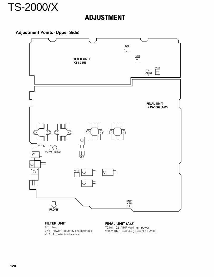
120
TS-2000/X
TC101 TC102
VR102
VR2
VR1
CN11VSR
TC1
VR1
TP1(AMD)
VR2
FILTER UNIT
(X51-315)
FINAL UNIT
(X45-360) (A/2)
FRONT
Adjustment Points (Upper Side)
FILTER UNITTC1 : NullVR1 : Power frequency characteristicVR2 : AT detection balance
FINAL UNIT (A/2)TC101,102 : VHF Maximum powerVR1,2,102 : Final idling current (HF/VHF)
ADJUSTMENT

121
TS-2000/X
W503
VULO2GND
TP502HCV
TP504UCV
L422L427
TP501HRCV
TP512VRCV
TP503VCV
TC402
I/11
K/11
TC400
TC401
J/11
TC409
TC410
TC408 D/11
TC403
E/11
TC406
TC404
G/11
TC405
H/11
L52
L28
TC2
L55
L34
L23
TC6
TC8
TC4TC5
TC10
TC13
TC12
TC14
CN414TX
L86
L82
L80
L93
SSM
CN15ADJ
TC3
L47
L44
TC1
CN19ADJ
TC9L90
L91
L164
L163
J1PADDLE
J2KEY
VR901TC901
VR902
CN906430ANT
TP506BCV
TP505HCV2
TX-RX 2 UNIT(X57-606) (B/11)
TX-RX 2 UNIT(X57-606) (A/11)
FINAL UNIT(X45-360) (B/2)TX-RX 2 UNIT
(X57-606) (C/11)
FRONT
Adjustment Points (Lower Side)
TX-RX 2 UNIT (B/11)L422,427 : 31.2MHz level
TX-RX 2 UNIT (D/11)TC403 : Lock volatge (HF REF VCO)
TX-RX 2 UNIT (E/11)TC406 : Lock volatge (VHF REF VCO)
TX-RX 2 UNIT (G/11)TC404 : Lock volatge (UHF PLL)
TX-RX 2 UNIT (K/11)TC400 : Lock volatge (SUB1 PLL)TC401 : Lock voltage (SUB2 PLL)
TX-RX 2 UNIT (A/11)L23,34,47,55,163,164 : MAIN VHF BPFL28,44,52 : Sub band BPFL80,82,86 : RX IF gain (VHF)L90,91,TC4~6,8,10 : TX BPF (UHF)L93 : Sub band FM discriminator coil (VHF)TC1~3,9 : MAIN UHF BPFTC9 : Trap frequency (UHF)TC12~14 : TX BPF (VHF)
FINAL UNIT (B/2)VR901,902 : Final idling current (UHF)TC901 : UHF maximum powe
TX-RX 2 UNIT (H/11)TC405 : Lock volatge (VHF MAIN PLL)
TX-RX 2 UNIT (I/11)TC402 : Lock voltage (HF LO2 PLL)
TX-RX 2 UNIT (J/11)TC408 : Lock voltage (HF1 MAIN PLL)TC409 : Lock voltage (HF3 MAIN PLL)TC410 : Lock voltage (HF2 MAIN PLL)
ADJUSTMENT

122
TS-2000/XADJUSTMENT
J6PANELJ5
D-SUB
L68L67
L69
L66 L65
CN9(TP5)
L64 L63 L62
TP2
L81 L82
TPNB
L87
S1
L613
L83
L614TP1
VR4
L71
L105
L103
L102
L54VR1
CN6(TP4)
J3SP2
J2SP1 J7
EXT. CONT
CN5
VR3 VR2
L100 L99 L98 L96
TP3
L108 L109
TC3
J8ACC2
L25
L34
L24 L23
L33 L32
L46 L45 L44
J4REMOTE
J1EXT RX
ANT
TC1
TC2
CN14HFTX
TX-RX 1 UNIT
(X57-605) (A/9)
FRONT
Adjustment Points (Lower Side)
TX-RX 1 UNIT (A/9)L23~25,32~34,44~46 : HF BPFL54,62~64,68 : MCF (69.085MHz)L65~67 : MCF (72.925MHz)L69,71,87,613,614 : HF RX IF gainL81,82 : NB gain
L83 : FM discriminator coil (HF)L96,98~100,102,103,105,108,109 : TX IF gain (HF)L96,98,99,100,102,VR3 : TX IF BPF (HF)VR1 : 1st mixer balanceVR2 : TX mixer balanceVR4 : Gain balanceTC1,2 : RX trap (E type only)TC3 : 29.1MHz frequency

123
TS-2000/X
FRONT
L399 L338
TC301
VR2 VR1
L340
L341
L342
TP2
CN16
L42 L43 L45
IC2
CN11
CN13
L321
L9
L5L320
CN14
CN15
L3
L2
L25
L22 L24
L26
L27 L28
L29
CN7 CN12
CN8
IC3
CN412ANT
CN14GND
CN512TIFGND
12RIFGND
TX-RX 3 UNIT
(X57-607)
1200MHz Adjustment Points
TX-RX 3 UNITL2,3,9 : TX IF gainL5,320,321 : MCF (135.395MHz)L22,24,25,29 : RX IF gainL26~28 : MCF (135.495MHz)L42,43,45 : LO level (Local osc)L338~342,VR1 : PLL reference levelVR2 : PLL reference spuriousTC301 : VCO control voltage
ADJUSTMENT
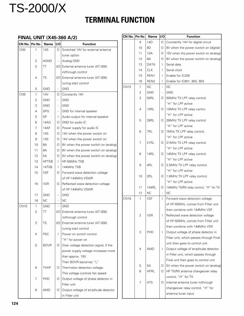
124
TS-2000/XTERMINAL FUNCTION
FINAL UNIT (X45-360 A/2)
CN No. Pin No. Name I/O Function
CN5 1 14S O Switched 14V for external antenna
tuner option
2 AGND - Analog GND
3 TT I/O External antenna tuner (AT-300)
in/through control
4 TS I/O External antenna tuner (AT-300)
tuning start control
5 GND - GND
CN9 1 14V O Constantly 14V
2 GND - GND
3 GND - GND
4 SPG - GND for internal speaker
5 SP I Audio output for internal speaker
6 14AG O GND for audio IC
7 14AF O Power supply for audio IC
8 14S O 14V when the power switch on
9 14S O 14V when the power switch on
10 8A O 8V when the power switch on (analog)
11 8A O 8V when the power switch on (analog)
12 5A O 5V when the power switch on (analog)
13 HFTXB I HF-50MHz TXB
14 14TXB I 144MHz TXB
15 VSF O Forward wave detection voltage
of HF-144MHz VSWR
16 VSR O Reflected wave detection voltage
of HF-144MHz VSWR
17 GND - GND
18 NC - NC
CN10 1 GND - GND
2 TT I/O External antenna tuner (AT-300)
in/through control
3 TS I/O External antenna tuner (AT-300)
tuning start control
4 PSC I Power on switch control.
“H” for power on
5 BOVR O Over voltage detection signal, if the
power supply voltage increases more
than approx. 19V.
Then BOVR becomes “L”
6 THHF O Thermistor detection voltage.
This voltage controls fan speed
7 PHD O Output voltage of phase detector in
Filter unit
8 AMD O Output voltage of amplitude detector
in Filter unit
CN No. Pin No. Name I/O Function
9 14D O Constantly 14V for digital circuit
10 8D O 8V when the power switch on (digital)
11 10A O 10V when the power switch on (analog)
12 8A O 8V when the power switch on (analog)
13 DATA I Serial data
14 CLK I Serial clock
15 REN1 I Enable for IC205
16 REN2 I Enable for IC801, 802, 803
CN15 1 NC - NC
2 GND - GND
3 50RL O 50MHz TX LPF relay control.
“H” for LPF active
4 10RL O 10MHz TX LPF relay contro.
“H” for LPF active
5 28RL O 28MHz TX LPF relay control.
“H” for LPF active
6 7RL O 7MHz TX LPF relay control.
“H” for LPF active
7 21RL O 21MHz TX LPF relay control.
“H” for LPF active
8 14RL O 14MHz TX LPF relay control.
“H” for LPF active
9 4RL O 3.5MHz TX LPF relay control.
“H” for LPF active
10 2RL O 1.8MHz TX LPF relay control.
“H” for LPF active
11 144RL O 144MHz TX/RX relay control. “H” for TX
12 NC - NC
CN16 1 VSF I Forward wave detection voltage
of HF-50MHz, comes from Filter unit
then combine with 144MHz VSF
2 VSR I Reflected wave detection voltage
of HF-50MHz, comes from Filter unit
then combine with 144MHz VSR
3 PHD I Output voltage of phase detector in
Filter unit, which passes through Final
unit then goes to control unit
4 AMD I Output voltage of amplitude detector
in Filter unit, which passes through
Final unit then goes to control unit
5 5A O 5V when the power switch on (analog)
6 HFRL O HF TX/RX antenna changeover relay
control, “H” for TX
7 ATS O Internal antenna tuner in/through
changeover relay control, “H” for
antenna tuner input

125
TS-2000/X
CN No. Pin No. Name I/O Function
8 ANT O Antenna 1/2 changeover relay control.
“H” for antenna 2
9 GND - GND
10 NC - NC
CN27 1 14S O 14V when the power switch on
2 GND - GND
3 GND - GND
FINAL UNIT (X45-360 B/2)
CN No. Pin No. Name I/O Function
CN902 1 UTHV O UHF thermal protection detection
voltage
2 43VSF O UHF forward wave detection
voltage
3 UTXB I UHF TX 8V
4 14S I 14V when the power switch on
5 14S I 14V when the power switch on
6 43VSR O UHF reflected wave detection voltage
7 GND - GND
8 GND - GND
FILTER UNIT (X51-315)
CN No. Pin No. Name I/O Function
CN9 1 NC - NC
2 GND - GND
3 50RL I 50MHz TX LPF relay control.
“H” for LPF active
4 10RL I 10MHz TX LPF relay control.
“H” for LPF active
5 28RL I 28MHz TX LPF relay control.
“H” for LPF active
6 7RL I 7MHz TX LPF relay control.
“H” for LPF active
7 21RL I 21MHz TX LPF relay control.
“H” for LPF active
8 14RL I 14MHz TX LPF relay control.
“H” for LPF active
9 4RL I 3.5MHz TX LPF relay control.
“H” for LPF active
10 2RL I 1.8MHz TX LPF relay control.
“H” for LPF active
11 144RL I 144MHz TX/RX relay control. “H” for TX
12 NC - NC
CN10 1 VSF O Forward wave detection voltage
of HF-50MHz, comes from Filter unit
then combine with 144MHz VSF
CN No. Pin No. Name I/O Function
2 VSR O Reflected wave detection voltage
of HF-50MHz, comes from Filter unit
then combine with 144MHz VSR
3 PHD O Output voltage of phase detector in
Filter unit, which passes through Final
unit then goes to control unit
4 AMD O Output voltage of amplitude detector
in Filter unit, which passes through
Final unit then goes to control unit
5 5A I 5V when the power switch on (analog)
6 HFRL I HF TX/RX antenna changeover relay
control. “H” for TX
7 ATS I Internal antenna tuner in/through
changeover relay control. “H” for
antenna tuner input
8 ANT I Antenna 1/2 changeover relay control.
“H” for antenna 2
9 GND - GND
10 NC - NC
CONTROL UNIT (X53-391)
CN No. Pin No. Name I/O Function
CN1 1 FEN2 O Enable
2 FEN1 O Enable
3 CLK O Serial clock
4 DATA O Serial data
5 8A I 8V when the power switch on (analog)
6 10A I 10V when the power switch on (analog)
7 8D I 8V when the power switch on (digital)
8 14D I Constantly 14V for digital circuit
9 AMD I Output voltage of amplitude detector
in Filter unit
10 PHD I Output voltage of phase detector in
Filter unit
11 THHF I Thermistor detection voltage.
This voltage controls fan speed
12 BOVR I Over voltage detection signal, if the
power supply voltage increases more
than approx. 19V.
Then BOVR becomes “L”
13 PSC O Power on switch control.
“H” for power on
14 TS I/O External antenna tuner (AT-300)
tuning start control
15 TT I/O External antenna tuner (AT-300)
in/through control
TERMINAL FUNCTION

126
TS-2000/X
CN No. Pin No. Name I/O Function
16 GND - GND
CN3 1 5V O 5V
2 GND - GND
3 PSW I Power switch, “L” for power on
4 INIT I “H” for CPU initialize
5 5D O Common 5V for LED
6 GND - GND
CN4 1 DGND - GND (Digital)
2 PBCK O Buck up signal (Sub CPU)
3 PCHK O Panel connection check
4 RES O Reset signal (Sub CPU)
5 TXDO I TX data (Main CPU)
6 RXDO O RX data (Main CPU)
7 RTSO I Data transmit inhibit signal (Main CPU)
8 CTSO O Data transmit inhibit signal (Main CPU)
9 5D O 5V (Digital)
10 8A O 8V (LED)
11 PRG3 -
12 PRG2 -
13 PRG1 -
14 PSW I Power switch output signal
15 5V -
16 10A O 10V (Lamp, PLL power supply)
17 GND - GND
18 GND - GND
CN5 1 NC - NC
2 GND - GND
3 THU I UHF thermal protection detection
voltage
4 GND - GND
5 SSM I Sub band S-meter input
6 SSQ I Sub band squelch input
7 SALT I Sub band auto lock tune input
8 SRBK O Sub band RF blanking signal
9 REN1 O IC2 enable
10 CLK O Serial clock
11 DATA O Serial data
12 NC - NC
13 KEY I Key down signal
14 KYS I Key jack judgement signal
15 DASH I Electronic keyer dash signal
16 DOT I Electronic keyer dot signal
17 GND - GND
18 NC - NC
CN6 1 GND - GND
2 12EN3 O Enable 3 for 1.2GHz unit
CN No. Pin No. Name I/O Function
3 12THV – Reserved
4 12UL I PLL unlock detect, “L” when 1.2GHz
PLL is unlocked
5 12EN2 O Enable 2 for 1.2GHz unit
6 12EN1 O Enable 1 for 1.2GHz unit
7 PDA O PLL data (1.2GHz unit)
8 PCK O PLL clock (1.2GHz unit)
9 CKY O CW keying, Active “H” to transmit
actual wave of all emission
10 MALT I Main auto lock tune (kind of auto
frequency control), main discriminator
DC output
11 DEN6 O DDS enable 6 (IC601)
12 DEN5 O DDS enable 5 (IC603)
13 DEN4 O DDS enable 4 (IC602)
14 IEN5 O IF enable 5 (IC15)
15 IEN4 O IF enable 4 (IC14)
16 IEN3 O IF enable 3 (IC17)
17 IEN2 O IF enable 2 (IC16)
18 IEN1 O IF enable 1 (IC5)
19 CLK O Serial clock
20 DATA O Serial data
21 ALCM I ALC meter voltage
22 VSRM I Reflected wave detection voltage
of HF-50MHz VSWR
23 VSFM I Forward wave detection voltage
of HF-50MHz VSWR
24 12RXC O 1.2GHz RX control,
Active “H” to enable 1.2GHz RX
25 12TXC O 1.2GHz TX control,
Active “H” to enable 1.2GHz TX
26 URXC O UHF RX control,
Active “H” to enable 430MHz RX
27 UTXC O UHF TX control,
Active “H” to enable 430MHz TX
28 VRXC O VHF RX control,
Active “H” to enable 144MHz RX
29 VTXC O VHF TX control,
Active “H” to enable 144MHz TX
30 HRXC O HF~50MHz RX control,
Active “H” to enable HF-50MHz RX
31 HTXC O HF~50MHz TX control,
Active “H” to enable HF-50MHz TX
32 MSQ I Main SQ signal output (detected
noise ; DC)
33 MSM I Main S-meter signal output
TERMINAL FUNCTION

127
TS-2000/X
CN No. Pin No. Name I/O Function
34 MRBK O Main receive blanking control.
“H” for blanking
35 AGCR O AGC reference voltage
36 BATT I Back up battery input for MODEM
CN7 1 10A O 10V (PLL power supply)
2 PDA O PLL serial data
3 PCK O PLL serial clock
4 DEN3 O DDS IC (IC407) enable
5 DEN2 O DDS IC (IC406) enable
6 DEN1 O DDS IC (IC408) enable
7 PEN6 O PLL IC (IC402) enable
8 PEN5 O PLL IC (IC401) enable
9 PEN4 O PLL IC (IC412) enable
10 PEN3 O PLL IC (IC410) enable
11 PEN2 O PLL IC (IC414) enable
12 PEN1 O PLL IC (IC409, 411) enable
13 PENA O Serial/parallel IC (IC404) enable
14 HFTXC O reserved
15 VTXC O VHF-TX control signal,
“H” when VHF TX is active
16 UTXC O UHF-TX control signal,
“H” when UHF TX is active
17 VRXC O VHF-RX control signal,
“H” when VHF main RX is active
18 URXC O UHF-RX control signal,
“H” when UHF main RX is active
19 UL I PLL unlock detection, “L” active
20 GND - GND
CN503 1 MIC I Mic signal input
2 MSG - Mic GND
3 MCG - GND
4 MU I Mic up signal
5 MD I Mic down signal
6 SS I Standby switch
7 8A O 8V (EXT Mic)
CN504 1 PRGS I “L” for MAIN CPU write
2 12OP I “H” when 1.2GHz unit installed
3 GND - GND
4 VO I VS-3 audio output
5 GND - GND
6 NAR O “H” for data input enable to VS-3
7 RST O VS-3 reset signal
8 VCS O VS3 voice synthesizer start signal
9 GND - GND
10 DRM O Audio in for DRU-3A
11 GND - GND
CN No. Pin No. Name I/O Function
12 DRO I Audio out from DRU-3A
13 GND - GND
14 EOM I End of message from DRU-3A.
“H” for end
15 DREN O Enable for DRU-3A voice recording
unit
16 STS O Start switch, active “H”. When START
is “H”, CPU get this signal then send
back STS to IF unit to turn ON IC10,
11, 604.
17 AMU O Audio Mute, Active “H” to mute SP1/
SP2 output
18 GND - GND
19 MANO O Main RX AF signal from DSP
20 GND - GND
21 SANO O Sub RX AF signal from DSP
22 GND - GND
23 PKD I Packet (modulation) data, packet
modulation data for DSP
24 GND - GND
25 SS I Standby switch, active low to TX
26 PKSA I Packet standby switch, active “L” to
packet TX
27 RTK I RTTY keying, active “L” to frequency
shift
28 SPS I Speaker switch, “OPEN” when SP2
is active
29 RXD1 I Level converted (5V) RXD
(J6 : REMORT PANEL)
30 TXD1 O Level converted (5V) TXD
(J6 : REMORT PANEL)
31 START I Active “H” when data comes from
REMOTE PANEL or PC
32 RXD2 O Level converted (5V) RXD
(J5 : RS-232C)
33 RTS2 I Level converted (5V) RTS
(J5 : RS-232C)
34 TXD2 I Level converted (5V) TXD
(J5 : RS-232C)
35 CTS2 O Level converted (5V) CTS
(J5 : RS-232C)
36 GND - GND
CN505 1 MAF O Main audio (SP1) output
2 GND - GND
3 SAF O Sub audio (SP2) output
4 GND - GND
TERMINAL FUNCTION

128
TS-2000/X
CN No. Pin No. Name I/O Function
CN506 1 MOD O Modulation output
2 GND - GND
3 MDET I Main band detection input
4 GND - GND
5 SDET I Sub band detection input
6 GND - GND
DISPLAY UNIT (X54-332)
CN No. Pin No. Name I/O Function
CN1 1 DGND - GND (Digital)
2 NC - NC
3 NC - NC
4 LRES I Reset signal (Dot LCD IC)
5 NC - NC
6 LCS4 I Chip selector 4 (Serial/parallel IC)
7 LCS3 I Chip selector 3 (Dot LCD IC)
8 LCS2 I Chip selector 2 (7 seg LCD IC)
9 LCS1 I Chip selector 1 (7 seg LCD IC)
10 LDA I LCD serial data
11 LCK I LCD serial clock
12 LMO I Mode set up signal (7 seg LCD IC)
13 LINH I Display inhibit signal (7 seg LCD IC)
14 5D I 5V (Digital)
15 KA O Key matrix output A
16 KB O Key matrix output B
17 KC O Key matrix output C
18 S0 I Key matrix input 0
19 S1 I Key matrix input 1
20 S2 I Key matrix input 2
21 S3 I Key matrix input 3
22 PSW O Power switch output signal
23 NC - NC
24 LEDB I LED power supply voltage
25 10A I 10V (Lamp)
26 GND - GND
TX-RX 1 UNIT (X57-605 A/9)
CN No. Pin No. Name I/O Function
CN16 1 MAF I Main audio (SP1) input from DSP
2 GND - GND
3 SAF I Sub audio (SP2) input from DSP
4 GND - GND
CN17 1 MOD I Modulation input, Modes other than
FM : 12kHz IF input, FM mode : AF input
2 GND - GND
CN No. Pin No. Name I/O Function
CN18 1 MDET O Main detect output, Modes other than
FM : 12kHz IF output, FM mode : AF
output
2 GND - GND
CN20 1 VCK I Clock for VS-3
2 VDT I Data for VS-3
3 VCS I VS-3 voice synthesizer start signal
4 RST I VS-3 reset signal
5 NAR I “H” for data input enable to VS-3
6 E - GND
7 5C I Common 5V
8 VO O VS-3 audio output
CN21 1 AGND - Analog GND
2 DRMG - AF GND
3 DRM I Audio input for DRU-3A
4 DRO O Audio output from DRU-3A
5 5D I Common 5V
6 DGND - Digital GND
7 EOM I End of message from DRU-3A “H” for end
8 NC - NC
9 DREN I Enable for DRU-3A voice recording unit
10 SD I Data for DRU-3A
11 SCK I Serial clock for DRU-3A
CN24 1 GND - GND
2 CTS2 I Level converted (5V) CTS (J5 : RS-232C)
3 TXD2 O Level converted (5V) TXD (J5 : RS-232C)
4 RTS2 O Level converted (5V) RTS (J5 : RS-232C)
5 RXD2 I Level converted (5V) RXD (J5 : RS-232C)
6 START O Active “H” when data comes from
REMOTE PANEL or PC
7 TXD1 I Level converted (5V) TXD
(J6 : REMORT PANEL)
8 RXD1 O Level converted (5V) RXD
(J6 : REMORT PANEL)
9 SPS O Speaker switch, “OPEN” when SP2 is active
10 RTK O RTTY keying, Active “L” to frequency shift
11 PKSA O Packet standby switch, active “L” to
packet TX
12 SS O Standby switch, active low to TX
13 GND - GND
14 PKD O Packet (modulation) data, packet
modulation data for DSP
15 GND - GND
16 SANO I Sub RX AF signal from DSP
17 GND - GND
18 MANO I Main RX AF signal from DSP
TERMINAL FUNCTION

129
TS-2000/X
CN No. Pin No. Name I/O Function
19 GND - GND
20 AMU I Audio Mute, active “H” to mute SP1/
SP2 output
21 STS I Start switch, active “H”. When START
is “H”, CPU gets this signal, then
send back STS to this unit to turn ON
IC10, 11, 604.
22 DREN I Enable for DRU-3A Voice recording unit
23 EOM O End of message from DRU-3A “H” for end
24 GND - GND
25 DRO O Audio out from DRU-3A
26 GND - GND
27 DRM I Audio in for DRU-3A
28 GND - GND
29 VCS I VS3 voice synthesizer start signal
30 RST I VS-3 reset signal
31 NAR I “H” for data input enable to VS-3
32 GND - GND
33 VO O VS-3 audio output
34 GND - GND
35 12OP O “H” when 1.2GHz unit installed
36 PRGS O “L” for MAIN CPU write
CN25 1 BATT O Back up battery output for MODEM
2 AGCR I AGC reference voltage
3 MRBK I Main receive blanking control.
“H” for blanking
4 MSM O Main S-meter signal output
5 MSQ O Main SQ signal output (detected
noise ; DC)
6 HTXC I HF~50MHz TX control,
Active “H” to enable HF-50MHz TX
7 HRXC I HF~50MHz RX control,
Active “H” to enable HF-50MHz RX
8 VTXC I VHF TX control,
Active “H” to enable 144MHz TX
9 VRXC I VHF RX control,
Active “H” to enable 144MHz RX
10 UTXC I UHF TX control,
Active “H” to enable 430MHz TX
11 URXC I UHF RX control,
Active “H” to enable 430MHz RX
12 12TXC I 1.2GHz TX control,
Active “H” to enable 1.2GHz TX
13 12RXC I 1.2GHz RX control,
Active “H” to enable 1.2GHz RX
CN No. Pin No. Name I/O Function
14 VSFM O Forward wave detection voltage
of HF-50MHz VSWR, amplified by
IC19
15 VSRM O Reflected wave detection voltage
of HF-50MHz VSWR, amplified by
IC19
16 ALCM O ALC meter voltage
17 DATA I Serial data
18 CLK I Serial clock
19 IEN1 I IF enable 1 (IC5)
20 IEN2 I IF enable 2 (IC16)
21 IEN3 I IF enable 3 (IC17)
22 IEN4 I IF enable 4 (IC14)
23 IEN5 I IF enable 5 (IC15)
24 DEN4 I DDS enable 4 (IC602)
25 DEN5 I DDS enable 5 (IC603)
26 DEN6 I DDS enable 6 (IC601)
27 MALT O Main auto lock tune (kind of auto
frequency control), main discriminator
DC output
28 CKY I CW keying, Active “H” to transmit
actual wave of all emission
29 PCK I PLL clock (1.2GHz unit)
30 PDA I PLL data (1.2GHz unit)
31 12EN1 I Enable 1 for 1.2GHz unit
32 12EN2 I Enable 2 for 1.2GHz unit
33 12UL O PLL unlock detect, “L” when 1.2GHz
PLL is unlocked
34 12THV - Reserved
35 12EN3 I Enable 3 for 1.2GHz unit
36 GND - GND
CN26 1 GND - GND
2 43VSF I Forward wave detection voltage
of 430MHz VSWR
3 14S O 14V when the power switch on
4 14S O 14V when the power switch on
5 43VSR I Reflected wave detection voltage
of 430MHz VSW
6 UTXB O 430MHz TXB approx. 8V
7 VTXB O 144MHz TXB approx. 8V
8 AGC O AGC
9 5C O Common 5V
10 TBPF O Control voltage for variable capacitor
of TX BPF
TERMINAL FUNCTION

130
TS-2000/X
CN No. Pin No. Name I/O Function
11 SBPF O Control voltage for variable capacitor
of SUB RX BPF
12 8C O Common 8V
13 MBPF O Control voltage for variable capacitor
of Main RX BPF
14 URXB O 430MHz RXB approx. 8V
15 VRXB O 144MHz RXB approx. 8V
16 UATT O UHF RX attenuater, “H” active
17 VATT O VHF RX attenuater, “H” active
18 GND - GND
CN27 1 GND - GND
2 12EN3 O Enable 3 for 1.2GHz unit
3 PCK O PLL clock (1.2GHz unit)
4 PDA O PLL data (1.2GHz unit)
5 12EN1 O Enable 1 for 1.2GHz unit
6 12EN2 O Enable 2 for 1.2GHz unit
7 12UL I PLL unlock detect, “L” when 1.2GHz
PLL is unlocled
8 12THV - Reserved
9 12OP I “H” when 1.2GHz unit installed
10 AGC O AGC voltage for 1.2GHz unit
11 12RXB O 1.2GHz RXB
12 12TXB O 1.2GHz TXB
13 NC - NC
14 5C O Common 5V
15 12VSR I Reflected wave detection voltage
of 1.2GHz VSWR
16 12VSF I Forward wave detection voltage
of 1.2GHz VSWR
17 GND - GND
18 NC - NC
CN29 1 14V I Constantly 14V
2 GND - GND
3 GND - GND
4 SPG - GND for internal speaker
5 SP O Audio output for internal speaker
6 14AG I GND for audio IC
7 14AF I Power supply for audio IC
8 14S I 14V when the power switch on
9 14S I 14V when the power switch on
10 8A I 8V when the power switch on (analog)
11 8A I 8V when the power switch on (analog)
12 5A I 5V when the power switch on (analog)
13 HFTXB O HF-50MHz TXB
14 14TXB O 144MHz TXB
CN No. Pin No. Name I/O Function
15 VSF I Forward wave detection voltage
of HF-144MHz VSWR
16 VSR I Reflected wave detection voltage
of HF-144MHz VSWR
17 GND - GND
18 NC - NC
CN31 1 SP1 O Main AF output to phone jack
2 SP2 I Main AF input from phone jack
3 PHG GND for phone jack
CN32 1 SP3 O Sub AF output to phone jack
2 SP4 I Sub AF input from phone jack
3 PHG - GND for phone jack
4 NC - NC
TX-RX 1 UNIT (X57-605 B/9)
CN No. Pin No. Name I/O Function
CN800 1 DGND - GND (Digital)
2 PBKC I Buck up signal (Sub CPU)
3 PCHK I Panel connection check
4 RES I Reset signal (Sub CPU)
5 TXD0 O TX data (Main CPU)
6 RXD0 I RX data (Main CPU)
7 RTS0 O Data transmit inhibit signal (Main CPU)
8 CTS0 I Data transmit inhibit signal (Main CPU)
9 5D I 5V (Digital)
10 8A I 8V (LED)
11 NC - NC
12 NC - NC
13 NC - NC
14 PSW O Power switch output signal
15 NC - NC
16 10A I 10V (Lamp, PLL power supply)
17 GND - GND
18 GND - GND
CN801 1 DGND - GND (Digital)
2 NC - NC
3 NC - NC
4 LRES O Reset signal (Dot LCD IC)
5 NC - NC
6 LCS4 O Chip selector 4 (Serial/parallel IC)
7 LCS3 O Chip selector 3 (Dot LCD IC)
8 LCS2 O Chip selector 2 (7 seg LCD IC)
9 LCS1 O Chip selector 1 (7 seg LCD IC)
10 LDA O LCD serial data
11 LCK O LCD serial clock
TERMINAL FUNCTION

131
TS-2000/X
CN No. Pin No. Name I/O Function
12 LMO O Mode set up signal (7 seg LCD IC)
13 LINH O Display inhibit signal (7 seg LCD IC)
14 5D O 5V (Digital)
15 KA I Key matrix input A
16 KB I Key matrix input B
17 KC I Key matrix input C
18 S0 O Key matrix output 0
19 S1 O Key matrix output 1
20 S2 O Key matrix output 2
21 S3 O Key matrix output 3
22 PSW I Power switch input signal
23 NC - NC
24 LEDB O LED power supply voltage
25 10A O 10V (Lamp)
26 GND - GND
CN804 1 5D O 5V (Encoder)
2 MENB I Main encoder pulse B
3 MENA I Main encoder pulse A
4 DGND - GND (Digital)
CN805 1 DGND - GND (Digital)
2 5D O 5V (Digital)
3 SUBS I Sub ON/OFF switch input signal
4 SSQL I Sub SQL VR analog voltage
5 SAF I Sub AF VR analog voltage
6 NC - NC
7 MUL2 I MULTI/CH encoder pulse 2
8 MUL1 I MULTI/CH encoder pulse 1
9 RITB I RIT/SUB encoder pulse 2
10 RITA I RIT/SUB encoder pulse 1
11 NC - NC
12 SUB O Control signal for SUB LED
13 MULTI O Control signal for MULTI LED
14 CON O Control signal for CON LED
15 STA O Control signal for STA LED
16 9.6K O Control signal for 9.6K LED
17 LEDB O LED power supply
18 NC - NC
CN806 1 5D O 5V (VR)
2 CWBC I CW beat cancel VR analog voltage
3 MRF I Main RF VR analog voltage
4 NC - NC
5 NC - NC
6 MAF I Main AF VR analog voltage
7 MSQL I Main SQL VR analog voltage
8 DGND - GND (Digital)
TX-RX 1 UNIT (X57-605 F/9)
CN No. Pin No. Name I/O Function
CN951 1 MIC O Mic signal output
2 MSG - Mic GND
3 MCG - GND
4 MU O Mic up signal
5 MD O Mic down signal
6 SS O Standby switch
7 8A I 8V (EXT Mic)
TX-RX 1 UNIT (X57-605 G/9)
CN No. Pin No. Name I/O Function
CN950 1 SP1 I Audio input for headphone
2 SP2 O Audio output when headphone through
3 PHG - GND for phone jack
4 SP3 I Audio input for headphone
5 SP4 O Audio output when headphone through
6 PHG - GND for phone jack
TX-RX 2 UNIT (X57-606 A/11)
CN No. Pin No. Name I/O Function
CN9 1 SDET O Sub RX detection output (144, 430MHz)
2 GND - GND
CN10 1 RIF O Main RX IF output (144, 430MHz)
2 GND - GND
CN12 1 UTHV I UHF thermal protection detection
voltage
2 43VSF I UHF forward wave detection
voltage
3 UTXB O UHF TX 8V
4 14S O 14V when the power switch on
5 14S O 14V when the power switch on
6 43VSR I UHF reflected wave detection
voltage
7 GND - GND
8 GND - GND
CN14 1 NC - NC
2 GND - GND
3 THU O UHF thermal protection detection
voltage
4 GND - GND
5 SSM O Sub band S-meter output
6 SSQ O Sub band squelch output
7 SALT O Sub band auto lock tune output
8 SRBK I Sub band RF blanking signal
TERMINAL FUNCTION

132
TS-2000/X
CN No. Pin No. Name I/O Function
9 REN1 I IC2 enable
10 CLK I Serial clock
11 DATA I Serial data
12 NC - NC
13 KEY O Key down signal
14 KYS O Key jack judgement signal
15 DASH O Electronic keyer dash signal
16 DOT O Electronic keyer dot signal
17 GND - GND
18 NC - NC
CN17 1 GND - GND
2 43VSF O Forward wave detection voltage
of 430MHz VSWR
3 14S I 14V when the power switch on
4 14S I 14V when the power switch on
5 43VSR O Reflected wave detection voltage
of 430MHz VSW
6 UTXB I 430MHz TXB approx. 8V
7 VTXB I 144MHz TXB approx. 8V
8 AGC I AGC
9 5C I Common 5V
10 TBPF I Control voltage for variable capacitor
of TX BPF
11 SBPF I Control voltage for variable capacitor
of SUB RX BPF
12 8C I Common 8V
13 MBPF I Control voltage for variable capacitor
of Main RX BPF
14 URXB I 430MHz RXB approx. 8V
15 VRXB I 144MHz RXB approx. 8V
16 UATT I VHF RX attenuater, “H” active
17 VATT I UHF RX attenuater, “H” active
18 GND - GND
TX-RX 2 UNIT (X57-606 B/11)
CN No. Pin No. Name I/O Function
CN501 1 10A I 10V (PLL power supply)
2 PDA I PLL serial data
3 PCK I PLL serial clock
4 DEN3 I DDS IC (IC407) enable
5 DEN2 I DDS IC (IC406) enable
6 DEN1 I DDS IC (IC408) enable
7 PEN6 I PLL IC (IC402) enable
8 PEN5 I PLL IC (IC401) enable
CN No. Pin No. Name I/O Function
9 PEN4 I PLL IC (IC412) enable
10 PEN3 I PLL IC (IC410) enable
11 PEN2 I PLL IC (IC414) enable
12 PEN1 I PLL IC (IC409, 411) enable
13 PENA I Serial/parallel IC (IC404) enable
14 HFTXC I HF-TX control signal
15 VTXC I VHF-TX control signal. “H” : VHF TX
16 UTXC I UHF-TX control signal. “H” : UHF TX
17 VRXC I VHF-RX control signal. “H” : VHF RX
18 URXC I UHF-RX control signal. “H” : UHF RX
19 UL O PLL unlock detection. “L” : Active
20 GND - GND
TX-RX 3 UNIT (X57-607)
CN No. Pin No. Name I/O Function
CN1 1 14S I 14V when the power switch on
2 GND - GND
CN5 1 12TIF I 1.2GHz TX IF (10.595MHz)
2 GND - GND
3 12RIF O 1.2GHz RX IF (10.695MHz)
4 GND - GND
CN6 1 GND - GND
2 12EN3 I Enable 3 for 1.2GHz unit
3 PCK I PLL clock (1.2GHz unit)
4 PDA I PLL data (1.2GHz unit)
5 12EN1 I Enable 1 for 1.2GHz unit
6 12EN2 I Enable 2 for 1.2GHz unit
7 12UL O PLL unlock detect, “L” when 1.2GHz
PLL is unlocled
8 12THV - Reserved
9 12OP O “H” when 1.2GHz unit installed
10 AGC I AGC voltage for 1.2GHz unit
11 12RXB I 1.2GHz RXB
12 12TXB I 1.2GHz TXB
13 NC - NC
14 5C I Common 5V
15 12VSR O Reflected wave detection voltage
of 1.2GHz VSWR
16 12VSF O Forward wave detection voltage
of 1.2GHz VSWR
17 GND - GND
18 NC - NC
TERMINAL FUNCTION

TS-2000/XTS-2000/X
134
WIRING

TRPNLJHFDB SQOMKIGECA
1
3
5
7
2
4
6
CIRCUIT DIAGRAM TS-2000/XNote : Components marked with a dot (·) are parts of pattern 1.
146

A B C D E F G H I J K L M N O P Q R S T U V W X Y Z AA AB AC AD AE AF AG AH AI AJ AK AL AM
1
2
3
4
5
6
7
8
9
10
11
12
13
14
1
2
3
4
5
6
7
8
9
10
11
12
13
14
C31 C35 C34 C36
X1
IC5
Q5
R5
R25
C26
C19
C50
8
C52
2
C52
5C
557
C56
1
C55
8
C55
9
C52
8
R55
5
R55
7
R55
8
R55
9
R56
0
R56
1
R56
3
C52
0 C50
5
C53
3C
531
C53
7
C54
7C
546
C54
9
X50
2
C54
8R
584
R57
3
R57
5
R57
6
R57
7
R57
8
R57
9
R58
0
R58
1
C54
0
C54
3
C56
3
C53
4R
567
O G IIC
502
X50
1
C53
5
D5
L15
R22
4
C18
2
C14
5
C15
3
C16
0C
159
C16
5R
162
R14
2
R16
1
R15
0
R59
4
R59
7R
598
R60
3
R60
6
R61
9
R62
6
R58
5
R13
5
C18
3
1 8916
IC6
IC7
R21
4
C68 C
32
C33R17
R16
R20
6
R20
7
R54
6
R54
7
R54
8
C14
7
C14
8
C55
2
C55
0
C59
4
C65
1
C60
1
C60
3
R71
2R
741
R72
1
C59
3
C60
0
C60
7
C61
1
C61
4
C62
5
C62
7 C63
8
C58
8
C71
6
C64
8
C63
6
R63
0
R63
7
R74
2
R64
2
R65
1
R65
9
R64
7
R74
3
R70
8
C18
5
1 8
1 458
IC13
1 7814
IC19
C74
R47
R48
R52
R53
R54
18 1
GN
DG
ND
10A 5V
PS
WP
RG
1P
RG
2P
RG
38A 5D
CT
SO
RT
SO
RX
DO
TX
DO
RE
SP
CH
KP
BK
CD
GN
D
NC
GN
DT
HU
GN
DS
SM
SS
QS
ALT
SR
BK
RE
N1
CLK
DA
TA NC
KE
YK
YS
DA
SH
DO
TG
ND
NC
1 101120
IC20
1 101120
IC21
C75
C76
C77
CP
501
5V
RE
SE
T
PS
W
INIT
5D GN
D
CN
3
1 6
MO
D
GN
D
MD
ET
GN
D
SD
ET
GN
D
CN
506
CN
505
1 6
MA
F
GN
D
SA
F
GN
D
1 4
CP
503
CP
502
C93
C94
C95
C96
C99
C10
0
C10
1
C10
3
C10
5
C10
7
C10
9
C11
1
C11
3
C11
5
C11
7
C11
9
C12
1
C12
3
C12
6
C97
C98
C10
2
C10
4
C10
6
C10
8
C11
0
C11
2
C11
4
C11
6
C11
8
C12
0
C12
2
C12
4
C12
5
C12
8
C12
9
C13
0
C13
1
C13
2
C13
3
C13
4
C13
5
C13
6
C13
7
C13
8
C13
9
C14
0
C14
1
C14
2
C14
3
C17
8
C71
7
C17
9
C67
6
C67
5
C67
4
C67
3
C67
2
C67
1
C67
0
C66
9
C66
8
C66
7
C66
6
C66
5
C66
4
C66
3
C66
2
GN
D12
EN
312
TH
V12
UL
12E
N2
12E
N1
PD
AP
CK
CK
YM
ALT
DE
N6
DE
N5
DE
N4
IEN
5IE
N4
IEN
3IE
N2
IEN
1C
LKD
ATA
ALC
MV
SR
MV
SFM
12R
XC
12T
XC
UR
XC
UT
XC
VR
XC
VT
XC
HR
XC
HT
XC
MS
QM
SM
MR
BK
AG
CR
BA
TT
361
C78
C79
L506
1 101120
IC22
1 101120
IC23
1 101120
IC24
1 101120
IC25
IC51
7
1
145 810
1120
IC14
1 7814
IC15
1 7814
IC16
1 7814
IC17
1 7814
IC18
1 7814
916
R209
R201
R202
R14
R15
R13
D15
CP4 CP3 CP6 CP5 CP8 CP7 CP10 CP9 CP12 CP11 CP14 CP13 CP16 CP15
CN4
1 18CN5
10A
PD
AP
CK
DE
N3
DE
N2
DE
N1
PE
N6
PE
N5
PE
N4
PE
N3
PE
N2
PE
N1
PE
NA
HFT
XC
VT
XC
UT
XC
VR
XC
UR
XC
UL
GN
D
1 20CN7
GN
DT
TT
SP
SC
BO
VR
TH
HF
PH
DA
MD
14D
8D 10A
8A DA
TAC
LKFE
N1
FEN
2
16 1CN1
R3 1
3 4
5IC33
4
5 1
3IC32
IC8
138
39
6465102
103
128
R216R217
D13
C188R223
R204
R26
C37
C23
C24
C21
C180
C503+
+ +
+
+
IC3
O
I
G
D6
D14C177
C174
C175
C169C158 C170
C171
C155
C592 C718
C164
IC26
12526
5051 75
76
100
R129
R136
R143 R145
R148 R599 R602R610 R618
R612
R611
R605
R139
R154 R159
R163
R160
R152
R153
R155
R120 R121 R122 R125C149
X3
D504
D11
D502
D503
D501
R213R702 R541
R542
R543
R544
IC530
1
10 11
20
R700
R553
R552
R554
C521
C524 C526 C527 C529C523
C504
C536
C539 C541 C542 C544C538
L16 L17
IC28
1
1213 24
25
3637
48
Q15
Q16
IC30
1
34
5
C551
C652R586
R720
IC5241
45
8IC525
5
81
4IC526
5
81
4IC527
1
45
8IC528
1
45
8
IC533
8
141
7
IC534
8
141
7
IC5295
81
4
IC531
8
141
7
IC532
8
141
7
C700
C602
R624
R623
C609
+
C92
CN6
PR
GS
12O
PG
ND
VO
GN
DN
AR
RS
TV
CS
GN
DD
RM
GN
DD
RO
GN
DE
OM
DR
EN
ST
SA
MU
GN
DM
AN
OG
ND
SA
NO
GN
DP
KD
GN
DS
SP
KS
AR
TK
SP
SR
XD
1T
XD
1S
TAR
TR
XD
2R
TS
2T
XD
2C
TS
2G
ND
361 CN504
R604+
C60
8
+
+
C61
0
C61
5
+
C62
9
+
C63
4
+
C63
9
+
C64
6
+
+
C61
6 C61
9
C63
0
Q50
1
+
C62
3
+
C62
2
+
C62
8
+
C64
1
+
C70
4
+
C64
4
+
C63
3
++
IC515
1
144 109
108
73
7237
36
IC516
1
144 109
108
73
7237
36
C530
C562 C560
C720C724
C725
C726
C727
C728
C721
C722
C723
C564
IC518
IC520
1
1
45
8
IC519
1
45
8
1415
28
C555+
C556+
R738 R701
C599+ C606+
X503
+
R568
R571
R570
+
IC521
9
16 1
8
IC522
13
24 1
12
IC523
13
24 1
12
C618 + C631
C617 C632
C642
C653
C703
C677
C678
C719
C643
C714
C713
C712
C711
8A
SS
MD
MU
MCG
MSG
MIC
7
1
CN503
C576
C545
C589
C590C577
C575
R631 R638
R710
R664
R643
R654
R592
R572
R648
R656
R655
R709
R706
R705
R707
C645
C654
R658
R657
+
+
C661
J72-0702-01
CONTROL UNIT (X53-391X-XX) 0-11 : K,KX 2-71 : E 2-72 : E2 Component side view
155
Component side
Foil side
Pattern 1Pattern 2Pattern 3Pattern 4
Ref No. Address IC3 4J IC5 4C IC6 5C IC7 6C IC8 5F IC13 8C IC14 8D IC15 8E IC16 8F IC17 8G IC18 8H IC19 9C IC20 9E IC21 9F IC22 9G IC23 9I IC24 9J IC25 9K IC26 6J IC28 6L IC30 7M IC32 4H IC33 3G IC502 3S IC515 4P IC516 4V IC517 9M IC518 7N IC519 7R
Ref No. Address IC520 7Q IC521 7T IC522 7V IC523 7X IC524 9N IC525 9P IC526 9R IC527 9T IC528 9U IC529 9W IC530 12K IC531 11N IC532 11P IC533 11V IC534 11X Q5 3G Q15 8L Q16 8M Q501 11U D5 4K D6 5K D11 12I D13 3H D14 5L D15 7D D501 11J D502 11I D503 12I D504 11I
TS-2000/X PC BOARD VIEWDAT124EKADTB143EKDTC114EEDTC124EKADTC143TKADTC143TUADTD123EK2SA11622SA1362
2SC3421
BE C
2SB11322SB11882SC33572SD1624
2SA1641
2SC26942SC3102
2SC19712SC1972
B E C
FMC2FMG1FMW1
5
3
21
2SC4093
12
3
4
FMA5UMC4
2SA1037K2SA1774
DTA114EKADTA114EUADTA143EKADTA143EUADTC114EKADTC114EUADTC143EUADTC144EUA
2SC4649
NJM2904MTC4W53FUTC7W74FU
NJM78L08UA
VIN
VREFGND
2SK302
2SK2082SK508NV2SK520
3SK1313SK241
2SK2685
2SK2596
3SK298
2SK2595
BU4066BCFVNJM2902MTC74VHC08FT
M62363FP
TC7SH08FUTC7S04FU
M57762-02M67715
LA4446
1
13
PST9130NRTA75S393F
BA10T
GN2011
UPD6345GS
TC74VHC573FT
ADM202EARUBU4094BCFVLMX2306TMXLMX2316TMXTC74HC4052AFTTC74HC4053AFTTC74VHC4040FT
TA7808S
NJU6433F
NJM2100VNJM2904VNJM5532MUPB1509GV
2SC27122SC33562SC3722K2SC41162SC46172SC50082SC50662SC5108

OMKIGECA NLJHFDB
1
3
5
7
2
4
6
CIRCUIT DIAGRAM TS-2000/X
185Note : Components marked with a dot (·) are parts of pattern 1.

TRPNLJHFDB SQOMKIGECA
1
3
5
7
2
4
6
CIRCUIT DIAGRAM TS-2000/X
204
Note : Components marked with a dot (·) are parts of pattern 1.

A C E G I K M O Q SB D F H J L N P R T
1
3
5
7
2
4
6
TS-2000/X CIRCUIT DIAGRAM
205
Note : Components marked with a dot (·) are parts of pattern 1.

AMALAKAJAIAHAGAFAEADACABAAZYXWVUTSRQPONMLKJIHGFEDCBA
1
2
3
4
5
6
7
8
9
10
11
12
13
14
1
2
3
4
5
6
7
8
9
10
11
12
13
14
R361
R366
R365 R364
R363
R367
R362
C371
C367
C400
C374
Q310
Q311
L343
R360 C370
C372
C378 C373
C39912EN3
L399L338
C375
C376
C377
C381
Q313
Q31414
23
14
23
C382
C384 C
385
C165
C304
C311
C314
C313
C153
C369
C368
C21
C84
C94
C91
R62
L336
C101
C85
R312
R386
R385
Q303
Q315
C302
C301
C156
C151
C136
C149
C148
C42
C318 R
6
R14
R12
R15
C11
C9
C12
L18C
54
C58
C63
L19
L20
L21
C57
C72
C65
C67
D3
C64
R46
R48
R49
C71
C70
C68
C315
D5
R45
C74
C327
C75
C60
C59
14S
GN
D
21
C44
C49
L17
CN
1
C305
C176
C180
Q17
C307
Q301
GD S
D305
D301
L346
L301
L303
L50L304
L305
R302
R307
R112
R301
R342
R105
R101
Q16
R102
R106
R95
R90
R333
R88
C79
C80
181
NC
GN
D12V
SF
12VS
R5CN
C12T
XB
12RX
BA
GC
12OP
12TH
V12U
L12E
N2
12EN
1P
DA
PC
K12E
N3
GN
D
TC
301
C320
C379
R369
R372
R371
R373
R370
L344
L49
L51R
379R
377
R376 R
378
12LO31
CN
9
C394
C392
Q312
VR
2
VR1
R368
R374
R375
C397
C387
C386
+
L340
L341
L342
TP2
+
C179+
C401
C391
C390
C393
R351
L345
CN16
L302
C306
C312
C309
C310
C172
C173
C308
C303
R303
R305R306
R304
CF1
CF2
C155
C398
C139
C138
R98
R89
R97
R335 R334
12EN2C131
R359
C195
C134
C194PCK
PDA
12EN1
12UL AGC
12TXB
12RXB
5C
CP2 CP1L39
L40
CN6
D12
Q13
R93
IC4
1
1415
28
+
Q302
L42 L43 L45
L52
A1
A2
L12
IC2
1 2 3 4 5
L10
CN11
CN13
L7L8
L321
R7
L9
L5
L320
CN14
XF2
CN
15
L3
L2
L25
L22L24
L26
L27 L28
L29
XF1
CN7 CN12
14S
CN8
L33
L30
CN2+B
CN3GND
12VF12VR
J72-0700-11
IC3
CN412ANT
CN14GND
CN5
L337
R19 R18 R17
+
+ +
C41
C40
C43
C45
C46
C48
C38
C15
L13
R43
C86
C404
R53
R51
R314
R311
R52 TH2
C7
R13
1 12TIF
GND
12RIF
GND4
C3
C2
L1
C53
C51
C52 C56
C55
1 2 3 4 5
+ +
+
C109
C61
C78
C76
R50
C66R44
R47
C69
D4
L309
D6
D7
D303
C128
L333
C127
C118
L35
R85
R79
R73
R71
R76
R78
R82
L32
L31
C125
C124 Q
12
D302
Q11
1 234
C123
C120
C122C
113
C104
C107
L308
L306
C106
C108
C105
R70
R81
R56
R54
R65
R64
L332
C328
C13
C10
C16
C18
L4
R2
R4
R9
Q1
Q2
123 4
123 4
R8
R11
R20
R31
L11
C402
R315
R36
R40
R39
R42
C32
C26
C36
C37
C34
D2
R30
R24
R27R
135
R132
R133
R127
R125R
124
R122
R120
R118
R309
R28
R25
R32
R108
R103
L312
R104
R94
R92
R91R
96
R111
C174
C169
R332
R330
R328
R326
R325
C336
C389
C333
Q306
Q307
C332
C335
C167IC
5
1 8916
C178
R99
C22
C158
C152
C150
C140
C143
C154
C145
R26Q
3
D1D
10D11
R384
C319
C193
C189
C183
C323
C184
C191
L310
C317
R321
R323
C1
C4
TH
1
R68
R63
R61
R60
C87
C95
C97C
93
C92
Q8
Q7
GD SG
D S
C88
R72
R75
C121
C119
L38
L37
L36
L34
C126
C326
C116
C111
C112
R86
R77
R83
R80
L322
L307
Q10
1
23
4
C103
A26
C117
C114 C110R74
D9
C99
C98
C96
R66
R67
R55
R57
R59 R58
L23
C316
C89C90
Q9
1
2 3
4
R319
R322
Q304 R3
R5C329
C6C5
C14C8
R10
R22R29
C19
C24
C20
R16L323
D8R23
R21
R134R130R131
C28
C27
C25
C29R34
A25
IC11
123
5
346
R35R37R38
R41
C33L315
L348 L318
L347
C403Q51
2 3
4
Q4
C190
C192
Q20
B
E
C
L319Q15
R100
R126
R123
R121
R119
R117
R310
C144C142
C135
C186
C185
C182C188
Q19
R87
C81
C133
C132
C82
C83
L44L41
C147C137
++
Q14
D304
R331R383
R329
R327
R324
C170
C383
C388
C395
C396
C171
Q305
C334++
+
R343
R381
PC BOARD VIEW TS-2000/XTX-RX 3 UNIT (X57-6070-00) Component side view + Foil Side : KX
218
Component side
Foil side
Pattern 1Pattern 2Pattern 3Pattern 4
Connect 1 and 4
Ref No. Address IC1 7L IC2 2N IC3 3U IC4 5H IC5 9E
Ref No. Address Q1 7Q Q2 7Q Q3 9N Q4 7L Q5 5K
Ref No. Address Q7 10P Q8 10Q Q9 10R Q10 11V Q11 10X
Ref No. Address Q12 10Z Q13 5I Q14 10H Q15 10J Q16 6G
Ref No. Address Q17 7G Q19 9I Q20 9K Q301 9G Q302 9H
Ref No. Address Q303 10P Q304 8Q Q305 8E Q306 7F Q307 7E
Ref No. Address Q310 3D Q311 3D Q312 10E Q313 5C Q314 5D
Ref No. Address Q315 11O D1 10M D2 5L D3 5Z D4 5AC
Ref No. Address D5 7AC D6 6AA D7 6AA D8 11O D9 10S
Ref No. Address D10 10L D11 10L D12 3I D301 8F D302 10Y
Ref No. Address D303 8Y D304 10E D305 8F
2SC3022
UMC2NUMW1
AD9851BRS
AK4524
AK4518M62364FPTC74LVX4245FS
LC73881M
320VC5402PGE
TA75W01FUTC7WU04FU
AT25128N10SI27TC7WH74FU
ADM3202ARUAD9835BRUTA31136FNTC74HC4050AFT
TC74VHC02FTTC74VHC04FTTC74VHC32FT
TA48M033FTA7805FTA7808F
FMA1A
UPC2709TB
TGT0210QTMT0111Q
M62003FPTA75W393FUTA4101FUPC1678G
BU2099FV
29LV800BAxxxxx29LV800BJxxxxx
30624FGAGxxxxx
64F2633xxxxSED1526F0A
X62FP1802PXC62FP3302P
2SC5125

A C E G I K M O Q SB D F H J L N P R T
1
3
5
7
2
4
6
TS-2000/X CIRCUIT DIAGRAM
219
Note : Components marked with a dot (·) are parts of pattern 1.

TS-2000/XTS-2000/X
–113dBm –112dBm–112.5dBm
–104dBm –109dBm –93dBm –100dBm –68dBm –67dBm
–108dBm
–103dBm–99dBm
–103dBm
–113dBm –96dBm –96dBm –92dBm –83dBm –87dBm –90dBm –72dBm –68dBm –90dBm –66dBm
–113dBm
–94dBm –102dBm –83dBm 1.9Vp-p0.4Vp-p
–113dBm
–83dBm–94dBm –73.5dBm –67.5dBm –76dBm –65dBm –53dBm –40dBm–46dBm
–47dBm –45.5dBm–41.5dBm
–41.5dBm–71dBm
–75dBm
–96dBm –87dBm –87dBm –78dBm
RFBPF
CN1HFRX
ANT
(0.4Vp-p) (2.0Vp-p)
Q12Q7 Q9
Q8 Q10
L51
XF1XF2
XF5XF6
Q18
Q15
Q25
L68
Q19
Q20
L71
Q38
L80
Q42
Q43
L86
L613CN10RIF
CN1112RIF
L614
Q700
Q701
12
14
IC18
Q709
IC3 Q42
CF1CF2CF3
Q38CF4
MDET
SDET6 1
IC525IC518
CODECIC522
CODEC
2
IC515
DSP2
IC516
DSP1 196 7 1 6
CN114RX
VHF
L9
MAINVHF
L23L34 Q24
L47L55
D48
IC423
45
XF1 Q61CN10RIF
Q37
SUBVHF
L28 Q22L44L52
D46
IC523
45
XF2
CN9SDET
L14
L15
Q14
CN243RX
UHF
CN412ANT
L8
MAINUHF
L108~111L137 Q21
L116~119L133
D49
SUBUHF
L29 Q25 L50
D91
L12
L13
IC7 : FM
916
Q9
L25
Q7
Q8
L22CN5
12RIF
5 96 7
IC2
455kHz
(455kHz) (AF 1kHz)
IC1 : FM
14.201MHz
VHF : 144.2MHz, UHF : 438.2MHz
69.085MHz 10.695MHz RIF 12kHz
–53.5dBm(0.68Vp-p)
IC527 IC9
0.16Vp-p45mVp-p
1.9Vp-p
SP
0.63V8Ω
CONTROL UNIT (X53-391)TX-RX 1 UNIT (X57-605 A/9) TX-RX 1 UNIT(X57-605 A/9)
41.895MHz 10.695MHz
58.525MHz AF 1kHz
TX-RX 2 UNIT (X57-606 A/11)
1270.4MHz 135.495MHz 10.695MHzTX-RX 3 UNIT (X57-607)
IC96 7
Q12 Q11 Q10L33 L30
XF1L26,28,29
Q303
AF 1kHz
LEVEL DIAGRAM (RX SECTION)
Measurement condition (TX-RX 1 unit)
Frequency : 14.2MHzPRE AMP : ONANT input : –113dBm/0.501µVAF output : 0.63V/8Ω, 1kHzMode : USBThe values in parentheses ( ) are those in FM mode.
Input –113dBm from the antenna, set AF VR so that AF output is 0.63V, and measure the signal level at each part.The AF section is measured with an oscilloscope and the other parts are measered with an RF voltmeter.
Measurement condition (TX-RX 2 unit)
Frequency : 144.0MHz (VHF), 438.2MHz (UHF)PRE AMP : ONANT input : –113dBm/0.501µVAF output : 0.63V/8Ω, 1kHzMode : USB (Main), FM (Sub)
Input –113dBm from CN1 and CN2, and measure the signal level at each part.All wires, except CN1 and CN2, are connected during measurement.The AF section is measured with an oscilloscope and the other parts are measered with an RF voltmeter.
Measurement condition (TX-RX 3 unit)
Frequency : 1270.4MHzANT input : –113dBm/0.501µVMode : USB
Input –113dBm from the 1.2GHz antenna connector and measure the signal level at each part.Use an RF voltmeter.
230229

TS-2000/XTS-2000/X
MIC
IC535 IC529 IC524
IC523
IC515IC516
IC518
DSP 6 11
IC6
Q54
XF9 Q711
L109 L108 L105
D84 D82Q49 Q48
L102
CN1112TIF
CN49TIF
Q46
Q47
Q44
Q45
L98
L91
Q46
Q47
L2 L5 L9L10
Q1
Q2
XF3 D54
–20.6dBm –5dBm –16dBm –5dBm
–17dBm –7dBm –13dBm
–20dBm –15dBm
+3.6dBm
+3.5dBm (1.4W) (7W) (20W) (65W)0dBm
L95
L96
Q43 Q1 Q2
Q3
Q4
Q6
Q7
Q101
Q102
CN14HFTX
CN1HFTX
CN214TX
Q901
L7L11
L13
L18
CN4HFPO
CN80314PO
CN4HFPIN HF/50MHz
ANT50W
HF/50MHz
VHF
14PIN VHFANT100W
CN18TIF Q17 Q26
Q18Q20
1 5
IC3 CN343TX
CN90143TX
CN414TX
Q304
Q3
480mVp-p370mVp-p750mVp-p600mVp-p
210mVp-p 3.0mW 10mW (1W) (13W)400mVp-p1.2Vp-p70mVp-p
Q902 Q903 Q905 LPFUHFANT50W
L320L321XF2
L7,8D1
MIX
L12
1 4
IC1 Q5
1 5
IC2
1 5
IC3
280mVp-p 440mVp-p 450mVp-p140mVp-p 450mVp-p
45mVp-p5mV 112mVp-p 81mVp-p
100mVp-p 100mVp-p 19mVp-p 240mVp-p41mVp-p 130mVp-p 30mVp-p 78mVp-p 50mVp-p 91mVp-p
430mVp-p 2.5Vp-p1.4Vp-p
6.0Vp-p4.5Vp-p
35Vp-p
36Vp-p 250Vp-p11Vp-p
230Vp-p
CONTROL UNIT (X53-391)AF 1kHz TIF 12kHz
TX-RX 1 UNIT (X57-605 A/9)10.595MHz 68.985MHz 14.2MHz
FINAL UNIT (X45-360 A/2)
FILTER UNIT(X51-315)
10.595MHz 41.795MHz 144MHz or 438MHzTX-RX 2 UNIT (X57-606 A/11) FINAL UNIT (X45-360 B/2)
12ANT10W
CN512TIF
1270.2MHz135.395MHz10.595MHzTX-RX 3 UNIT (X57-607)
Measurement condition (TX-RX 1 unit)
Frequency : 14.2MHzMIC input : 1kHz/5mVOutput power : 100W (HF, VHF), 50W (UHF)MIC level : ALC zone maximum
Audio frequency section is measured by the AF voltmeter or oscilloscope.Radio frequency section is measured by the RF voltmeter or oscilloscope.The value in parentheses ( ) for the final unit (X45-360 B/2) is a reference value.
Measurement condition (TX-RX 2 unit)Frequency : 144MHz (VHF), 438MHz (UHF)MIC input : 1kHz/5mVOutput power : 100W (VHF), 50W (UHF)MIC level : ALC zone maximum
Measure the power using the RF voltmeter.
Measurement condition (TX-RX 3 unit)Frequency : 1270MHzMIC input : 1kHz/5mVOutput power : 10WMIC level : ALC zone maximum
Measure the voltage or power using the oscilscope or spectrum analyzer.
LEVEL DIAGRAM (TX SECTION)
231 232

233
TS-2000/XMC-52DM (MULTI-FUNCTION MICROPHONE WITH DTMF)
External View
SpecificationsType .......................................................... Electret capacitorPower requirement ...................................... 8.0V DC ± 10%Current drain .................................................... 35mA or lessDimensions (WxHxD) ................................ 65 x 90 x 30 mm
2-9/16 x 3-17/32 x 1-13/16 inWeight ................................................. Approx. 180g / 6.3ozSensitivity .................–70dB±3dB (at 1kHz) (0dB = 1V/µbar)
Parts List
Ref. No. New Parts No. Description
parts
A02-1982-08 Case (Front)A02-1983-08 Case (Rear)
E30-3243-08 Microphone cord assy (Metal)
K29-5101-08 Knob (PTT)K29-5102-08 Knob (Up, Down)K29-5103-08 Key top (20 key)K29-5104-08 Knob (Lock)
SW3,4 S40-1117-05 Tact switch (Up, Down)SW2 S62-0441-08 Slide switch (Lock)SW1 S70-0465-08 Tact switch (PTT)
T91-0570-08 Microphone element
IC1 LR40872 ICQ1-3 2SC1623 Transistor
Connector End ViewMetal plug (8P)
1
8
MIC
GND
7GND (MIC)
6NC
58V DC
2 STBY (PTT)
3 DWN
4 UP
Item Condition Test equipment / Measurement Adjustment Specifications / Remarks
DTMF [3], [6] key at VR1 2.4mV±0.01mVoutput level same time push
12
345
67
8
0.01
µF
5.6k
Ω
B (8V)
GND
+
–
8P metalplug
AF VTVM
–
+
Adjustment

23
4
TS
-2000/XM
C-52DM (M
ULTI-FUNCTION
MICROPHON
E WITH DTM
F)
Sch
am
atic
Dia
gra
m

235
TS-2000/XUT-20 (1200MHz All Mode Unit) / RC-2000 (Mobile Controller) /
ARCP-2000 (Radio Control Program)
UT-20 External View
Service center installation only.Contact an authorized dealer for details.
RC-2000 External View
ARCP-2000 External View
System requirements :
• IBM PC/AT and compatible machines with Microsoft®
Windows®95 or Windows®98.• Intel®Pentium®75MHz or higher processor (Pentium®
133MHz or higher recommended).• CD-ROM Drive• 800 x 600 screen resolution or higher.• Mouse or compatible pointing device.• RS-232C (Serial port)• 6MB of RAM or higher.• At least 5MB of available hard-disk space.

236
TS-2000/X
GeneralMode ........................................................................................... J3E (LSB, USB) A1A (CW) A3E (AM) F3E (FM) F1D (FSK) F2DNumber of memory channels .................................................... 300Antenna impedance ................................................................... 50Ω (With antena tuner 16.7 to 150Ω)Supply voltage ............................................................................ DC 13.8V ± 15%Ground method .......................................................................... Negative groundCurrent
Transmit (Max.) ....................................................................... 20.5A or lessReceive (No signal) ................................................................. 2.6A or less
Usable temperature range ......................................................... –10°C to +50°C (+14°F to +122°F)Frequency stability (–10°C to +50°C)
Main Other mode ............................................................. Within ±0.5 x 10⁻⁶ (Within ±0.5ppm)FM mode ................................................................. ±0.5 x 10⁻⁶ ±2kHz
Sub .......................................................................................... ±0.5 x 10⁻⁶ ±600HzFrequency accuracy (at room temperature)
Main Other mode ............................................................. ±0.5 x 10⁻⁶ (±0.5ppm)FM mode ................................................................. ±0.5 x 10⁻⁶ ±500Hz
Sub .......................................................................................... ±0.5 x 10⁻⁶ ±600HzDimensions (W x H x D) ............................................................. 270 x 96 x 317 mm / 10.6 x 3.8 x 12.5 in
(Projections included) ............................................................. (281 x 107 x 371 mm / 11.1 x 4.2 x 14.6 in)Weight ........................................................................................ TS-2000 : Approx. 7.8kg (17.2 lbs) TS-2000X : Approx. 8.2kg (18.1 lbs)
TransmitterFrequency range
160m band .............................................................................. 1.8 to 2.0MHz (K) 1.81 to 2.0MHz (E) 1.83 to 1.85MHz (E2)80m band ................................................................................ 3.5 to 4.0MHz (K) 3.5 to 3.8MHz (E,E2)40m band ................................................................................ 7.0 to 7.3MHz (K) 7.0 to 7.1MHz (E,E2)30m band ................................................................................ 10.1 to 10.15MHz20m band ................................................................................ 14.0 to 14.35MHz17m band ................................................................................ 18.068 to 18.168MHz15m band ................................................................................ 21.0 to 21.45MHz12m band ................................................................................ 24.89 to 24.99MHz10m band ................................................................................ 28.0 to 29.7MHz6m band .................................................................................. 50.0 to 54.0MHz (K) 50.0 to 52.0MHz (E) 50.0 to 50.2MHz (E2)2m band .................................................................................. 144 to 148MHz (K) 144 to 146MHz (E,E2)70cm band .............................................................................. 430 to 450MHz (K) 430 to 440MHz (E,E2)23cm band .............................................................................. 1240 to 1300MHz (TS-2000X)
Output powerSSB/CW/FSK/FM Max. ...................................................... 100W (1.8 to 144MHz) / 50W (430 (440) MHz) / 10W (1.2GHz)
Min. ...................................................... 5W (1.8 to 144MHz) / 5W (430 (440) MHz) / 1W (1.2GHz)AM Max. ...................................................... 25W (1.8 to 144MHz) / 12.5W (430 (440) MHz) / 2.5W (1.2GHz)
Min. ...................................................... 5W (1.8 to 144MHz) / 5W (430 (440) MHz) / 1W (1.2GHz)Modulation
SSB .......................................................................................... BalancedFM ........................................................................................... ReactanceAM ........................................................................................... Low level
Spurious emissions1.8 to 29.7MHz ....................................................................... –50dB or less50.0 to 440 (450) MHz ............................................................ –60dB or less1240 to 1300MHz ................................................................... –50dB or less
Carrier suppression .................................................................... 50dB or moreUnwanted sideband suppression (Modulation frequency 1.0kHz) ...... 50dB or moreMaximum frequency deviation (FM)
Wide ........................................................................................ ±5kHz or lessNarrow .................................................................................... ±2.5kHz or less
XIT shift frequency range ........................................................... ±20.0kHzMicrophone impedance.............................................................. 600Ω
SPECIFICATIONS

237
TS-2000/X
ReceiverCircuit type
Main band SSB/CW/AM/FSK .............................................. Quadruple conversion superheterodyneFM ..................................................................... Triple conversion superheterodyne
Sub band FM/AM .............................................................. Duble conversion superheterodyneFrequency range ( ) : VFO coverage range
Main band ............................................................................... 0.5 to 30MHz, 50 to 54MHz (0.03 to 60.0MHz)144 to 148MHz (K) (142 to 152MHz (K)) 144 to 146MHz (E,E2)430 to 145MHz (K) (420 to 450MHz (K)) 430 to 440MHz (E,E2)1240 to 1300MHz (TS-2000X)
Sub band ................................................................................. 144 to 148MHz (K) (118 to 174MHz (K)) 144 to 146MHz (E,E2)438 to 450MHz (K) (220 to 512MHz (K)) 430 to 440MHz (E,E2)
Intermediate frequency (IF)Main transceiver 1st IF ..................................................... HF/50MHz band : 69.085MHz or 75.925MHz
144/430 (440)MHz band : 41.895MHz 1200MHz band : 135.495MHz2nd IF .................................................... 10.695MHz3rd IF .................................................... 455kHz4th IF .................................................... 12.0kHz
Sub receiver 1st IF ..................................................... 58.525MHz2nd IF .................................................... 455kHz
SensitivityMain band SSB/CW/FSK (S/N 10dB) .................................. 0.5 to 1.705MHz : 4µV or less
1.705 to 24.5MHz : 0.2µV or less24.5 to 30.0MHz : 0.13µV or less50.0 to 54.0MHz : 0.13µV or less144 to 146MHz : 0.11µV or less (E,E2)144 to 148MHz : 0.16µV or less (K)430 to 440MHz : 0.11µV or less (E,E2)430 to 450MHz : 0.11µV or less (K)1240 to 1300MHz : 0.11µV or less
AM (S/N 10dB) .................................................. 0.5 to 1.705MHz : 31.6µV or less1.705 to 24.5MHz : 2.0µV or less24.5 to 30.0MHz : 1.3µV or less50.0 to 54.0MHz : 1.3µV or less144 to 146MHz : 1.0µV or less (E,E2)144 to 148MHz : 1.4µV or less (K)430 to 440MHz : 1.0µV or less (E,E2)430 to 450MHz : 1.0µV or less (K)1240 to 1300MHz : 1.0µV or less
FM (12dB SINAD) ............................................. 28.0 to 30.0MHz : 0.22µV or less50.0 to 54.0MHz : 0.22µV or less144 to 146MHz : 0.18µV or less (E,E2)144 to 148MHz : 0.25µV or less (K)430 to 440MHz : 0.18µV or less (E,E2)430 to 450MHz : 0.18µV or less (K)1240 to 1300MHz : 0.18µV or less
Sub band AM (S/N 10dB) .................................................. 144 to 146MHz : 1.55µV or less (E,E2)144 to 148MHz : 2.25µV or less (K)430 to 440MHz : 1.55µV or less (E,E2)438 to 450MHz : 1.55µV or less (K)
FM (12dB SINAD) ............................................. 144 to 146MHz : 0.28µV or less (E,E2)144 to 148MHz : 0.40µV or less (K)430 to 440MHz : 0.28µV or less (E,E2)438 to 450MHz : 0.28µV or less (K)
SelectivityMain band SSB (Low cut : 300Hz / Hi cut : 2600Hz) .......... –6dB : 2.2kHz –60dB : 4.4kHz
AM (Low cut : 100Hz / Hi cut : 3000Hz) ........... –6dB : 6.0kHz –50dB : 12.0kHzFM ..................................................................... –6dB : 12.0kHz –50dB : 25.0kHz
Sub band AM ..................................................................... –6dB : 12.0kHz –50dB : 25.0kHzFM ..................................................................... –6dB : 12.0kHz –50dB : 25.0kHz
SPECIFICATIONS

KENWOOD CORPORATION14-6, Dogenzaka 1-chome, Shibuya-ku, Tokyo 150-8501, Japan
KENWOOD SERVICE CORPORATIONP.O. BOX 22745, 2201 East Dominguez Street, Long Beach, CA 90801-5745, U.S.A.
KENWOOD ELECTRONICS CANADA INC.6070 Kestrel Road, Mississauga, Ontario, Canada L5T 1S8
KENWOOD ELECTRONICS DEUTSCHLAND GMBHRembrücker Str. 15, 63150 Heusenstamm, Germany
KENWOOD ELECTRONICS BELGIUM N.V.Mechelsesteenweg 418 B-1930 Zaventem, Belgium
KENWOOD ELECTRONICS FRANCE S.A.13, Boulevard Ney, 75018 Paris, France
KENWOOD ELECTRONICS U.K. LIMITEDKENWOOD House, Dwight Road, Watford, Herts., WD1 8EB United Kingdom
KENWOOD ELECTRONICS EUROPE B.V.Amsterdamseweg 37, 1422 AC Uithoorn, The Netherlands
KENWOOD ELECTRONICS ITALIA S.p.A.Via G. Sirtori, 7/9 20129 Milano, Italy
KENWOOD IBERICA S.A.Bolivia, 239-08020 Barcelona, Spain
KENWOOD ELECTRONICS AUSTRALIA PTY. LTD.(A.C.N. 001 499 074)16 Giffnock Avenue, North Ryde, N.S.W. 2113 Australia
KENWOOD ELECTRONICS (HONG KONG) LTD.Unit 3712-3724, Level 37, Tower one Metroplaza, 223 Hing Fong Road, Kwai Fong, N.T., Hong Kong
KENWOOD ELECTRONICS TECHNOLOGIES(S) PTE LTD.TE LTD.Sales Marketing Division1 Ang Mo Kio Street 63, Singapore 569110
TS-2000/X
Image rejectionMain transceiver ..................................................................... 70dB or moreSub transceiver ....................................................................... 60dB or more
1st IF rejectionMain transceiver ..................................................................... 70dB or moreSub transceiver ....................................................................... 60dB or more
Notch filter attenuation (at 1kHz) ............................................... 30dB or moreBeat cancel attenuation (at 1kHz) .............................................. 40dB or moreRIT shift frequency range ........................................................... ±20.0kHzSquelch sensitivity
Main band SSB/CW/FSK/AM .............................................. 0.5 to 1.705MHz : 18.0µV or less1.8 to 28.7MHz : 1.8µV or less50.0 to 54.0MHz : 1.1µV or less144 to 146MHz : 1.1µV or less (E,E2)144 to 148MHz : 1.1µV or less (K)430 to 440MHz : 1.1µV or less (E,E2)430 to 450MHz : 1.1µV or less (K)1240 to 1300MHz : 1.1µV or less
FM ..................................................................... 28.0 to 30.0MHz : 0.2µV or less50.0 to 54.0MHz : 0.2µV or less144 to 146MHz : 0.1µV or less (E,E2)144 to 148MHz : 0.16µV or less (K)430 to 440MHz : 0.1µV or less (E,E2)430 to 450MHz : 0.1µV or less (K)1240 to 1300MHz : 0.1µV or less
Sub band AM ..................................................................... 144 to 146MHz : 1.1µV or less (E,E2)144 to 148MHz : 1.1µV or less (K)430 to 440MHz : 1.1µV or less (E,E2)438 to 450MHz : 1.1µV or less (K)
FM ..................................................................... 144 to 146MHz : 0.18µV or less (E,E2)144 to 148MHz : 0.23µV or less (K)430 to 440MHz : 0.18µV or less (E,E2)438 to 450MHz : 0.18µV or less (K)
Audio output (8Ω, 10% distortion) ............................................. 1.5W or moreAudio output impedance (EXT. SP1 and EXT. SP2) ................... 4~8Ω
Specifications are subject to change without notice orobligation due to ongoing technological developments.
SPECIFICATIONS
Related Documents