SERVICE MANUAL COPYRIGHT © 2008 Victor Company of Japan, Limited No.MA427<Rev.001> 2008/8 NAVIGATION/DVD RECEIVER MA427<Rev.001> 2008 8 SERVICE MANUAL KW-NX7000J, KW-NX7000E, KW-NX7000EE COPYRIGHT © 2008 Victor Company of Japan, Limited Lead free solder used in the board (material : Sn-Ag-Cu, melting point : 219 Centigrade) Lead free solder used in the board (material : Sn-Cu, melting point : 230 Centigrade) TABLE OF CONTENTS 1 PRECAUTION. . . . . . . . . . . . . . . . . . . . . . . . . . . . . . . . . . . . . . . . . . . . . . . . . . . . . . . . . . . . . . . . . . . . . . . . . 1-6 2 SPECIFIC SERVICE INSTRUCTIONS . . . . . . . . . . . . . . . . . . . . . . . . . . . . . . . . . . . . . . . . . . . . . . . . . . . . . . 1-9 3 DISASSEMBLY . . . . . . . . . . . . . . . . . . . . . . . . . . . . . . . . . . . . . . . . . . . . . . . . . . . . . . . . . . . . . . . . . . . . . . . 1-9 4 ADJUSTMENT . . . . . . . . . . . . . . . . . . . . . . . . . . . . . . . . . . . . . . . . . . . . . . . . . . . . . . . . . . . . . . . . . . . . . . . 1-23 5 TROUBLESHOOTING . . . . . . . . . . . . . . . . . . . . . . . . . . . . . . . . . . . . . . . . . . . . . . . . . . . . . . . . . . . . . . . . . 1-38 Only for KW-NX7000E Only for KW-NX7000E/EE Only for KW-NX7000EE Only for KW-NX7000J

Welcome message from author
This document is posted to help you gain knowledge. Please leave a comment to let me know what you think about it! Share it to your friends and learn new things together.
Transcript

SERVICE MANUAL
COPYRIGHT © 2008 Victor Company of Japan, Limited No.MA427<Rev.001>2008/8
NAVIGATION/DVD RECEIVERMA427<Rev.001>20088SERVICE MANUAL
KW-NX7000J, KW-NX7000E, KW-NX7000EE
COPYRIGHT © 2008 Victor Company of Japan, Limited
Lead free solder used in the board (material : Sn-Ag-Cu, melting point : 219 Centigrade)Lead free solder used in the board (material : Sn-Cu, melting point : 230 Centigrade)
TABLE OF CONTENTS1 PRECAUTION. . . . . . . . . . . . . . . . . . . . . . . . . . . . . . . . . . . . . . . . . . . . . . . . . . . . . . . . . . . . . . . . . . . . . . . . . 1-62 SPECIFIC SERVICE INSTRUCTIONS . . . . . . . . . . . . . . . . . . . . . . . . . . . . . . . . . . . . . . . . . . . . . . . . . . . . . . 1-93 DISASSEMBLY . . . . . . . . . . . . . . . . . . . . . . . . . . . . . . . . . . . . . . . . . . . . . . . . . . . . . . . . . . . . . . . . . . . . . . . 1-94 ADJUSTMENT . . . . . . . . . . . . . . . . . . . . . . . . . . . . . . . . . . . . . . . . . . . . . . . . . . . . . . . . . . . . . . . . . . . . . . . 1-235 TROUBLESHOOTING . . . . . . . . . . . . . . . . . . . . . . . . . . . . . . . . . . . . . . . . . . . . . . . . . . . . . . . . . . . . . . . . . 1-38
Only for KW-NX7000E
Only for KW-NX7000E/EE
Only for KW-NX7000EE
Only for KW-NX7000J
1-2 (No.MA427<Rev.001>)
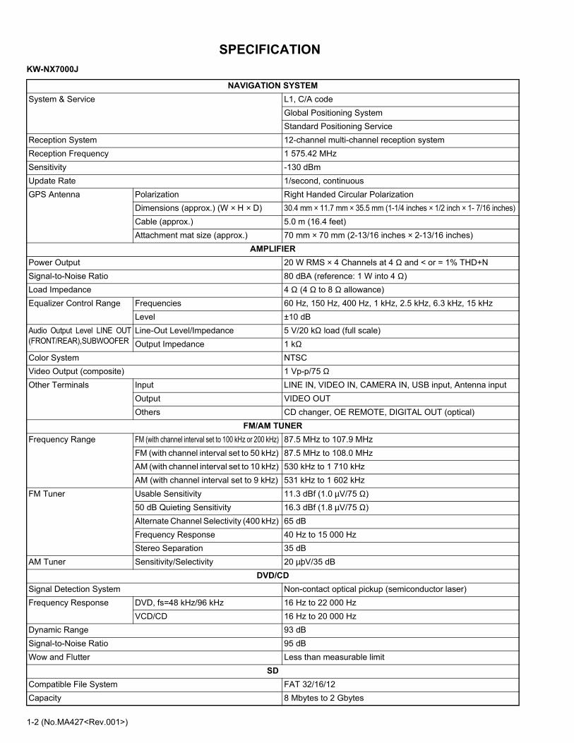
SPECIFICATIONKW-NX7000J
NAVIGATION SYSTEMSystem & Service L1, C/A code
Global Positioning SystemStandard Positioning Service
Reception System 12-channel multi-channel reception systemReception Frequency 1 575.42 MHzSensitivity -130 dBmUpdate Rate 1/second, continuousGPS Antenna Polarization Right Handed Circular Polarization
Dimensions (approx.) (W × H × D) 30.4 mm × 11.7 mm × 35.5 mm (1-1/4 inches × 1/2 inch × 1- 7/16 inches)Cable (approx.) 5.0 m (16.4 feet)Attachment mat size (approx.) 70 mm × 70 mm (2-13/16 inches × 2-13/16 inches)
AMPLIFIERPower Output 20 W RMS × 4 Channels at 4 Ω and < or = 1% THD+NSignal-to-Noise Ratio 80 dBA (reference: 1 W into 4 Ω)Load Impedance 4 Ω (4 Ω to 8 Ω allowance)Equalizer Control Range Frequencies 60 Hz, 150 Hz, 400 Hz, 1 kHz, 2.5 kHz, 6.3 kHz, 15 kHz
Level ±10 dBAudio Output Level LINE OUT(FRONT/REAR),SUBWOOFER
Line-Out Level/Impedance 5 V/20 kΩ load (full scale)Output Impedance 1 kΩ
Color System NTSCVideo Output (composite) 1 Vp-p/75 ΩOther Terminals Input LINE IN, VIDEO IN, CAMERA IN, USB input, Antenna input
Output VIDEO OUTOthers CD changer, OE REMOTE, DIGITAL OUT (optical)
FM/AM TUNERFrequency Range FM (with channel interval set to 100 kHz or 200 kHz) 87.5 MHz to 107.9 MHz
FM (with channel interval set to 50 kHz) 87.5 MHz to 108.0 MHzAM (with channel interval set to 10 kHz) 530 kHz to 1 710 kHzAM (with channel interval set to 9 kHz) 531 kHz to 1 602 kHz
FM Tuner Usable Sensitivity 11.3 dBf (1.0 µV/75 Ω)50 dB Quieting Sensitivity 16.3 dBf (1.8 µV/75 Ω)Alternate Channel Selectivity (400 kHz) 65 dBFrequency Response 40 Hz to 15 000 HzStereo Separation 35 dB
AM Tuner Sensitivity/Selectivity 20 µþV/35 dBDVD/CD
Signal Detection System Non-contact optical pickup (semiconductor laser)Frequency Response DVD, fs=48 kHz/96 kHz 16 Hz to 22 000 Hz
VCD/CD 16 Hz to 20 000 HzDynamic Range 93 dBSignal-to-Noise Ratio 95 dBWow and Flutter Less than measurable limit
SDCompatible File System FAT 32/16/12Capacity 8 Mbytes to 2 Gbytes

(No.MA427<Rev.001>)1-3
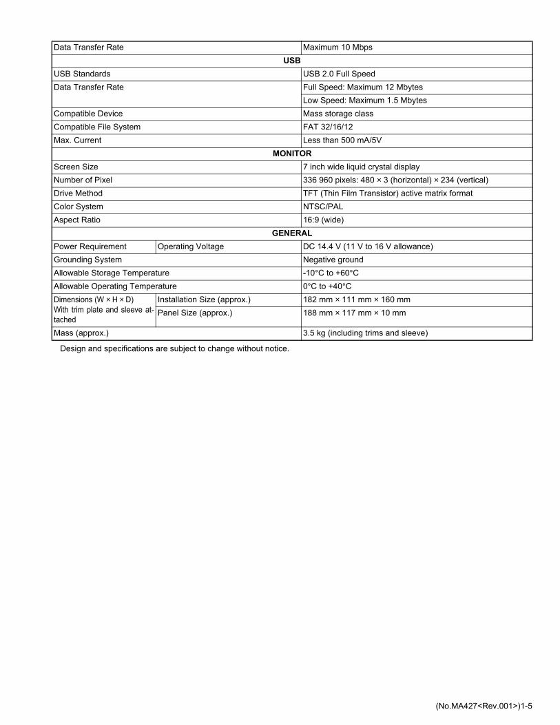
Data Transfer Rate Maximum 10 MbpsUSB
USB Standards USB 2.0 Full SpeedData Transfer Rate Full Speed: Maximum 12 Mbytes
Low Speed: Maximum 1.5 MbytesCompatible Device Mass storage classCompatible File System FAT 32/16/12Max. Current Less than 500 mA/5V
MONITORScreen Size 7 inch wide liquid crystal displayNumber of Pixel 336 960 pixels: 480 × 3 (horizontal) × 234 (vertical)Drive Method TFT (Thin Film Transistor) active matrix formatColor System NTSC/PALAspect Ratio 16 : 9 (wide)
GENERALPower Requirement Operating Voltage DC 14.4 V (11 V to 16 V allowance)Grounding System Negative groundAllowable Storage Temperature -10°C to +60°C (14°F to 140°F)Allowable Operating Temperature 0°C to +40°C (32°F to 104°F)Dimensions (W × H × D)With trim plate and sleeve at-tached
Installation Size (approx.) 182 mm × 111 mm × 160 mm(7-3/16” × 4-3/8” × 6-5/16”)
Panel Size (approx.) 188 mm × 117 mm × 10 mm(7-7/16” × 4-5/8” × 7/16”)
Mass (approx.): 3.5 kg (7.8 lbs) (including trims and sleeve)

1-4 (No.MA427<Rev.001>)
KW-NX7000E/ EE
NAVIGATION SYSTEMSystem & Service L1, C/A code
Global Positioning SystemStandard Positioning Service
Reception System 12-channel multi-channel reception systemReception Frequency 1 575.42 MHzSensitivity -130 dBmUpdate Rate 1/second, continuousGPS Aerial Polarization Right Handed Circular Polarization
Dimensions (approx.) (W × H × D) 30.4 mm × 11.7 mm × 35.5 mmCable (approx.) 5.0 mAttachment mat size (approx.) 70 mm × 70 mm
AMPLIFIERMaximum Power Output Front/Rear 50 W per channelContinuous Power Output (RMS) Front/Rear 20 W per channel into 4 Ω, 40 Hz to 20 000 Hz at no more than
0.8% total harmonic distortionLoad Impedance 4 Ω (4 Ω to 8 Ω allowance)Equalizer Control Range Frequencies 60 Hz, 150 Hz, 400 Hz, 1 kHz, 2.5 kHz, 6.3 kHz, 15 kHz
Level ±10 dBSignal-to-Noise Ratio 70 dBAudio Output Level LINE OUT (FRONT/REAR), SUBWOOFER
Line-Out Level/Impedance 5 V/20 kΩ load (full scale)Output Impedance 1 kΩ
Color System PALVideo Output (composite) 1 Vp-p/75 ΩOther Terminals Input LINE IN, VIDEO IN, CAMERA IN, USB input, Aerial input
Output VIDEO OUTOthers CD changer, OE REMOTE, DIGITAL OUT (optical)
FM/AM TUNERFrequency Range FM 87.5 MHz to 108.0 MHz
AM (MW) 522 kHz to 1 620 kHz(LW) 144 kHz to 279 kHz
FM Tuner Usable Sensitivity 11.3 dBf (1.0 µV/75 Ω)50 dB Quieting Sensitivity 16.3 dBf (1.8 µV/75 Ω)Alternate Channel Selectivity (400 kHz) 65 dBFrequency Response 40 Hz to 15 000 HzStereo Separation 35 dB
MW Tuner Sensitivity/Selectivity 20 µV/35 dBLW Tuner Sensitivity 50 µV
DVD/CDSignal Detection System Non-contact optical pickup (semiconductor laser)Frequency Response DVD, fs=48 kHz/96 kHz 16 Hz to 22 000 Hz
VCD/CD 16 Hz to 20 000 HzDynamic Range 93 dBSignal-to-Noise Ratio 95 dBWow and Flutter Less than measurable limit
SDCompatible File System FAT 32/16/12Capacity 8 Mbytes to 2 Gbytes
(No.MA427<Rev.001>)1-5
Design and specifications are subject to change without notice.
Data Transfer Rate Maximum 10 MbpsUSB
USB Standards USB 2.0 Full SpeedData Transfer Rate Full Speed: Maximum 12 Mbytes
Low Speed: Maximum 1.5 MbytesCompatible Device Mass storage classCompatible File System FAT 32/16/12Max. Current Less than 500 mA/5V
MONITORScreen Size 7 inch wide liquid crystal displayNumber of Pixel 336 960 pixels: 480 × 3 (horizontal) × 234 (vertical)Drive Method TFT (Thin Film Transistor) active matrix formatColor System NTSC/PALAspect Ratio 16:9 (wide)
GENERALPower Requirement Operating Voltage DC 14.4 V (11 V to 16 V allowance)Grounding System Negative groundAllowable Storage Temperature -10°C to +60°CAllowable Operating Temperature 0°C to +40°CDimensions (W × H × D) With trim plate and sleeve at-tached
Installation Size (approx.) 182 mm × 111 mm × 160 mmPanel Size (approx.) 188 mm × 117 mm × 10 mm
Mass (approx.) 3.5 kg (including trims and sleeve)

1-6 (No.MA427<Rev.001>)
SECTION 1PRECAUTION
1.1 Safety Precautions(1) This design of this product contains special hardware and
many circuits and components specially for safety purpos-es. For continued protection, no changes should be madeto the original design unless authorized in writing by themanufacturer. Replacement parts must be identical tothose used in the original circuits. Services should be per-formed by qualified personnel only.
(2) Alterations of the design or circuitry of the product shouldnot be made. Any design alterations of the product shouldnot be made. Any design alterations or additions will voidthe manufacturers warranty and will further relieve themanufacture of responsibility for personal injury or propertydamage resulting therefrom.
(3) Many electrical and mechanical parts in the products havespecial safety-related characteristics. These characteris-tics are often not evident from visual inspection nor can theprotection afforded by them necessarily be obtained by us-ing replacement components rated for higher voltage, watt-age, etc. Replacement parts which have these specialsafety characteristics are identified in the Parts List of Ser-vice Manual. Electrical components having such featuresare identified by shading on the schematics and by ( ) onthe Parts List in the Service Manual. The use of a substitutereplacement which does not have the same safety charac-teristics as the recommended replacement parts shown inthe Parts List of Service Manual may create shock, fire, orother hazards.
(4) The leads in the products are routed and dressed with ties,clamps, tubings, barriers and the like to be separated fromlive parts, high temperature parts, moving parts and/orsharp edges for the prevention of electric shock and firehazard. When service is required, the original lead routingand dress should be observed, and it should be confirmedthat they have been returned to normal, after reassem-bling.
(5) Leakage shock hazard testingAfter reassembling the product, always perform an isola-tion check on the exposed metal parts of the product (an-tenna terminals, knobs, metal cabinet, screw heads,headphone jack, control shafts, etc.) to be sure the productis safe to operate without danger of electrical shock.Do notuse a line isolation transformer during this check.• Plug the AC line cord directly into the AC outlet. Using a
"Leakage Current Tester", measure the leakage currentfrom each exposed metal parts of the cabinet, particular-ly any exposed metal part having a return path to thechassis, to a known good earth ground. Any leakage cur-rent must not exceed 0.5mA AC (r.m.s.).
• Alternate check methodPlug the AC line cord directly into the AC outlet. Use anAC voltmeter having, 1,000Ω per volt or more sensitivityin the following manner. Connect a 1,500Ω 10W resistorparalleled by a 0.15µF AC-type capacitor between an ex-posed metal part and a known good earth ground.Measure the AC voltage across the resistor with the AC
voltmeter. Move the resistor connection to each exposed metalpart, particularly any exposed metal part having a returnpath to the chassis, and measure the AC voltage acrossthe resistor. Now, reverse the plug in the AC outlet andrepeat each measurement. Voltage measured any mustnot exceed 0.75 V AC (r.m.s.). This corresponds to 0.5mA AC (r.m.s.).
1.2 Warning(1) This equipment has been designed and manufactured to
meet international safety standards.(2) It is the legal responsibility of the repairer to ensure that
these safety standards are maintained.(3) Repairs must be made in accordance with the relevant
safety standards.(4) It is essential that safety critical components are replaced
by approved parts.(5) If mains voltage selector is provided, check setting for local
voltage.
1.3 CautionBurrs formed during molding may be left over on some partsof the chassis. Therefore, pay attention to such burrs in the case of pre-forming repair of this system.
1.4 Critical parts for safetyIn regard with component parts appearing on the silk-screenprinted side (parts side) of the PWB diagrams, the parts that areprinted over with black such as the resistor ( ), diode ( )and ICP ( ) or identified by the " " mark nearby are criticalfor safety. When replacing them, be sure to use the parts of thesame type and rating as specified by the manufacturer. (This regulation dose not Except the J and C version)
Good earth ground
Place this probe on each exposedmetal part.
AC VOLTMETER(Having 1000 ohms/volts,or more sensitivity)
1500 10W
0.15 F AC TYPE

(No.MA427<Rev.001>)1-7
1.5 Preventing static electricityElectrostatic discharge (ESD), which occurs when static electricity stored in the body, fabric, etc. is discharged, can destroy the laserdiode in the traverse unit (optical pickup). Take care to prevent this when performing repairs.1.5.1 Grounding to prevent damage by static electricityStatic electricity in the work area can destroy the optical pickup (laser diode) in devices such as laser products. Be careful to use proper grounding in the area where repairs are being performed.
(1) Ground the workbenchGround the workbench by laying conductive material (such as a conductive sheet) or an iron plate over it before placing thetraverse unit (optical pickup) on it.
(2) Ground yourselfUse an anti-static wrist strap to release any static electricity built up in your body.
(3) Handling the optical pickup• In order to maintain quality during transport and before installation, both sides of the laser diode on the replacement optical
pickup are shorted. After replacement, return the shorted parts to their original condition. (Refer to the text.)
• Do not use a tester to check the condition of the laser diode in the optical pickup. The tester's internal power source can easilydestroy the laser diode.
1.6 Handling the traverse unit (optical pickup)(1) Do not subject the traverse unit (optical pickup) to strong shocks, as it is a sensitive, complex unit. (2) Cut off the shorted part of the flexible cable using nippers, etc. after replacing the optical pickup. For specific details, refer to the
replacement procedure in the text. Remove the anti-static pin when replacing the traverse unit. Be careful not to take too long atime when attaching it to the connector.
(3) Handle the flexible cable carefully as it may break when subjected to strong force. (4) I t is not possible to adjust the semi-fixed resistor that adjusts the laser power. Do not turn it.
1.7 Attention when traverse unit is decomposed*Please refer to "Disassembly method" in the text for the pickup unit. • Apply solder to the short land sections before the card wire is disconnected from the connecto on the servo board. (If the card wire
is disconnected without applying solder, the pickup may be destroyed by static electricity.)• In the assembly, be sure to remove solder from the short land sections after connecting the card wire.
1M
Conductive material
(conductive sheet) or iron palate
(caption)
Anti-static wrist strap
Solder short part

1-8 (No.MA427<Rev.001>)
1.8 Important for laser products
1.CLASS 1 LASER PRODUCT
2.CAUTION : (For U.S.A.) Visible and/or invisible class II laser radiation when open. Do not stare into beam. (Others) Visible and/or invisible class 1M laser radiation when open. Do not view directly with optical instruments.
3.CAUTION : Visible and/or invisible laser radiation when open and inter lock failed or defeated. Avoid direct exposure to beam.
4.CAUTION : This laser product uses visible and/or invisible laser radiation and is equipped with safety switches which prevent emission of radiation when the drawer is open and the safety interlocks have failed or are defeated. It is dangerous to defeat the safety switches.
5.CAUTION : If safety switches malfunction, the laser is able to function.
6.CAUTION : Use of controls, adjustments or performance of procedures other than those specified here in may result in hazardous radiation exposure.
REPRODUCTION AND POSITION OF LABELS and PRINT
! Please use enough caution not to
see the beam directly or touch it
in case of an adjustment or operation
check.
WARNING LABEL and PRINT

(No.MA427<Rev.001>)1-9
SECTION 2SPECIFIC SERVICE INSTRUCTIONS
This service manual does not describe SPECIFIC SERVICE INSTRUCTIONS.
SECTION 3DISASSEMBLY
3.1 Main body 3.1.1 Removing the Heat sink (See Fig.1)
(1) Remove the three screws A and four screws B attachingthe Heat sink.
Fig.1
3.1.2 Removing the Rear bracket (See Fig.2 to 4)(1) Remove the three screws C attaching the Rear heat
sink.(See Fig.2)(2) Remove the ten screws D and one screw E attaching the
rear bracket. (See Fig.3)(3) Disconnect the connector wire from Car cable connected to
connector CN601 of the Sub board. (See Fig.4)(4) Disconnect the connector wire from Fan connected to con-
nector CN604 of the Sub board. (See Fig.4)(5) Disconnect the card wire from Main board connected to
connector CN605 of the Sub board. (See Fig.4)(6) Disconnect the connector wire from Main board connected
to connector CN607 of the Sub board. (See Fig.4)
Fig.2
Fig.3
Fig.4
A
B
B
C
E
D
D D
CN605 CN607 CN601 CN604
1-10 (No.MA427<Rev.001>)
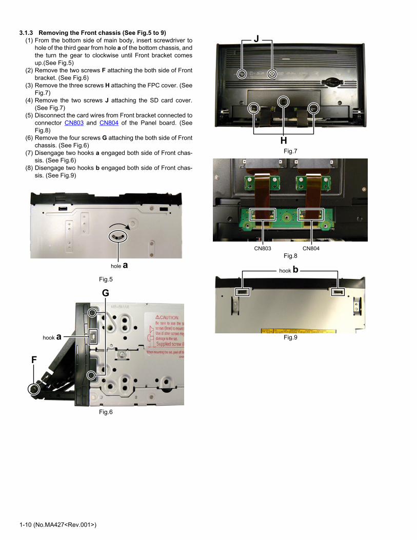
3.1.3 Removing the Front chassis (See Fig.5 to 9)(1) From the bottom side of main body, insert screwdriver to
hole of the third gear from hole a of the bottom chassis, andthe turn the gear to clockwise until Front bracket comesup.(See Fig.5)
(2) Remove the two screws F attaching the both side of Frontbracket. (See Fig.6)
(3) Remove the three screws H attaching the FPC cover. (SeeFig.7)
(4) Remove the two screws J attaching the SD card cover.(See Fig.7)
(5) Disconnect the card wires from Front bracket connected toconnector CN803 and CN804 of the Panel board. (SeeFig.8)
(6) Remove the four screws G attaching the both side of Frontchassis. (See Fig.6)
(7) Disengage two hooks a engaged both side of Front chas-sis. (See Fig.6)
(8) Disengage two hooks b engaged both side of Front chas-sis. (See Fig.9)
Fig.5
Fig.6
Fig.7
Fig.8
Fig.9
hole a
hook a
F
G
J
H
CN803 CN804
hook b

(No.MA427<Rev.001>)1-11
3.1.4 Removing the Top chassis (See Fig.10 to 13)(1) Remove the two screws K attaching the Front board. (See
Fig.10)(2) Disconnect the card wire from Main board connected to
connector CN983 of the Sub board. (See Fig.11)(3) Remove the four screws L attaching the both side of Top
chassis. (See Fig.12, 13)
Fig.10
Fig.11
Fig.12
Fig.13
K
CN983
L
L
1-12 (No.MA427<Rev.001>)
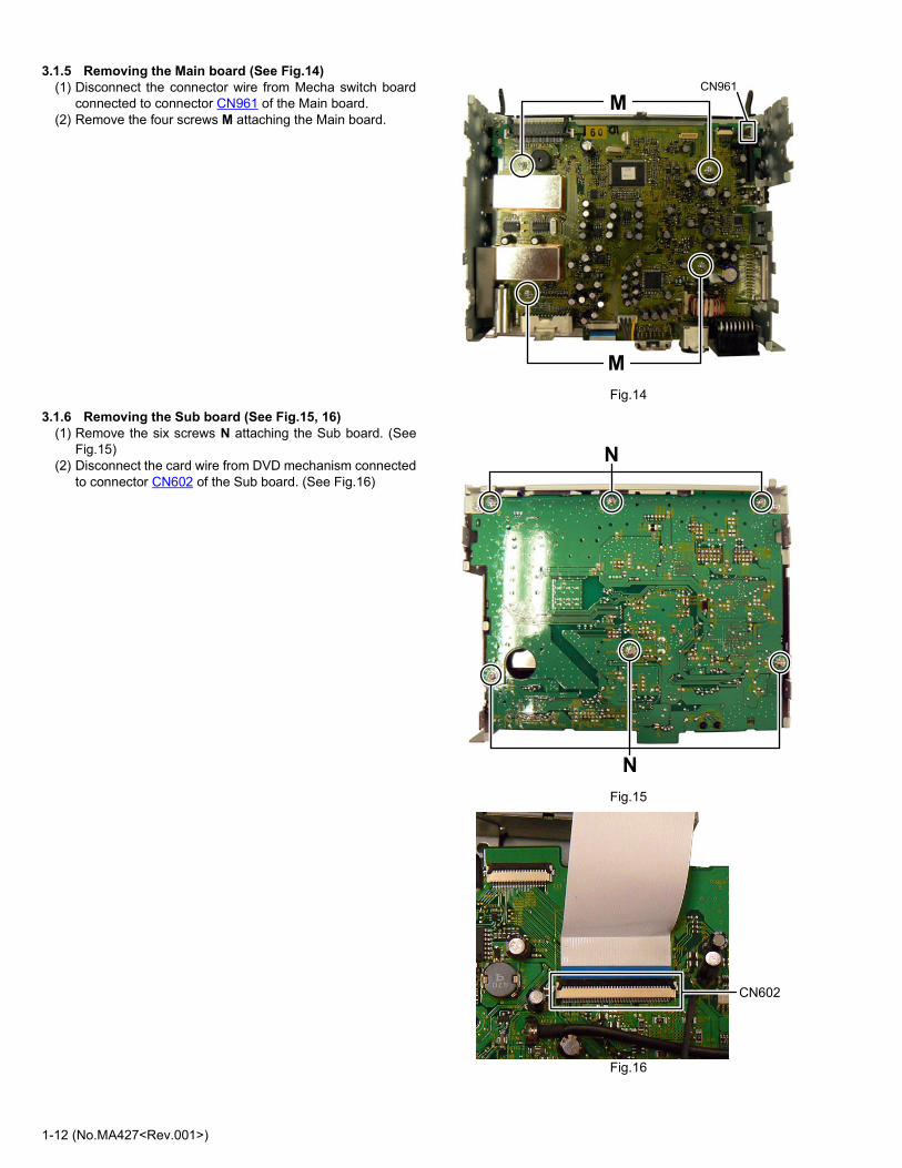
3.1.5 Removing the Main board (See Fig.14)(1) Disconnect the connector wire from Mecha switch board
connected to connector CN961 of the Main board.(2) Remove the four screws M attaching the Main board.
Fig.14
3.1.6 Removing the Sub board (See Fig.15, 16)(1) Remove the six screws N attaching the Sub board. (See
Fig.15)(2) Disconnect the card wire from DVD mechanism connected
to connector CN602 of the Sub board. (See Fig.16)
Fig.15
Fig.16
M
M
CN961
N
N
CN602

(No.MA427<Rev.001>)1-13
3.1.7 Removing the Navi board and the DVD mechanism(See Fig.17 to 21)
(1) Remove the two screws P attaching the Front board brack-et.(See Fig.17)
(2) Remove the three screws Q attaching the Navi shieldtop.(See Fig.18)
(3) Remove the four screws R attaching the Navi shield bot-tom.(See Fig.19)
(4) Remove the four screws S attaching the CPU bracket.(SeeFig.20)
(5) Remove the three screws T attaching the DVD mecha-nism.(See Fig.21)
Fig.17
Fig.18
Fig.19
Fig.20
Fig.21
P
Q
Q
Navi shield top
R
R
Navi shield bottom
S
S
T
T

1-14 (No.MA427<Rev.001>)
3.1.8 Removing the Motor board (See Fig.22, 23)(1) Remove the four screws U attaching the Mid chassis.
(See Fig.22)(2) Remove the three screws V attaching the Motor board.
(See Fig.23)
Fig.22
Fig.23
U
U
V

(No.MA427<Rev.001>)1-15
3.2 Monitor section 3.2.1 Removing the Rear cover (See Fig.1 to 3)
(1) Remove the ten screws A and five screws B attaching theRear cover. (See Fig.1, 2)
(2) Disconnect the card wire from Panel board connected toconnector CN881 of the Connection board. (See Fig.3)
Fig.1
Fig.2
Fig.3
A
A
A
A
B
B
CN881

1-16 (No.MA427<Rev.001>)
3.2.2 Removing the Connection board (See Fig.4)(1) Remove the five screws C attaching the Connection board.
Fig.4
3.2.3 Removing the Panel board (See Fig.5)(1) Disconnect the connector wire from LCD module connect-
ed to connector CN403 of the Panel board.(2) Disconnect the card wire from LCD module connected to
connector CN401 of the Panel board.(3) Disconnect the card wire from Switch board connected to
connector CN501 and CN502 of the Panel board.(4) Remove the four screws D attaching the Panel board.
Fig.5
3.2.4 Removing the LCD module (See Fig.6)(1) Disengage six hooks a engaged Panel bracket.
Fig.6
C
C
D
D
D
DCN501 CN502CN401
CN403
hook a
hook a
(No.MA427<Rev.001>)1-17
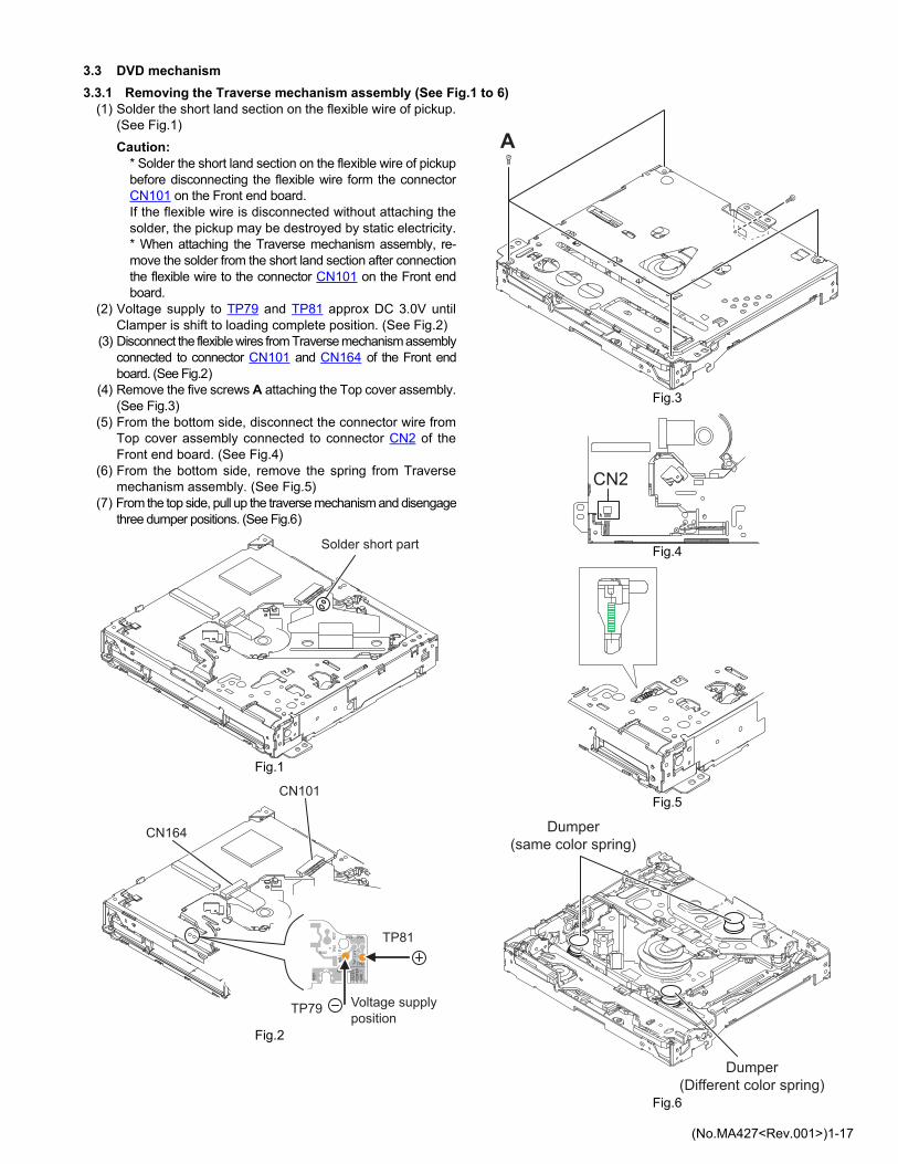
3.3 DVD mechanism3.3.1 Removing the Traverse mechanism assembly (See Fig.1 to 6)
(1) Solder the short land section on the flexible wire of pickup.(See Fig.1)
Caution:* Solder the short land section on the flexible wire of pickupbefore disconnecting the flexible wire form the connectorCN101 on the Front end board.If the flexible wire is disconnected without attaching thesolder, the pickup may be destroyed by static electricity.* When attaching the Traverse mechanism assembly, re-move the solder from the short land section after connectionthe flexible wire to the connector CN101 on the Front endboard.
(2) Voltage supply to TP79 and TP81 approx DC 3.0V untilClamper is shift to loading complete position. (See Fig.2)
(3) Disconnect the flexible wires from Traverse mechanism assemblyconnected to connector CN101 and CN164 of the Front endboard. (See Fig.2)
(4) Remove the five screws A attaching the Top cover assembly.(See Fig.3)
(5) From the bottom side, disconnect the connector wire fromTop cover assembly connected to connector CN2 of theFront end board. (See Fig.4)
(6) From the bottom side, remove the spring from Traversemechanism assembly. (See Fig.5)
(7) From the top side, pull up the traverse mechanism and disengagethree dumper positions. (See Fig.6)
Fig.1
Fig.2
Fig.3
Fig.4
Fig.5
Fig.6
Solder short part
CEN
TERR21
D-
DG
ND
_7
R312
R31
7
WO
OFE
R
TP67
R35
7
TP79 TP81
TP92
Voltage supply
position
CN164
CN101
TP81
TP79
A
CN2
Dumper
(same color spring)
Dumper
(Different color spring)
1-18 (No.MA427<Rev.001>)
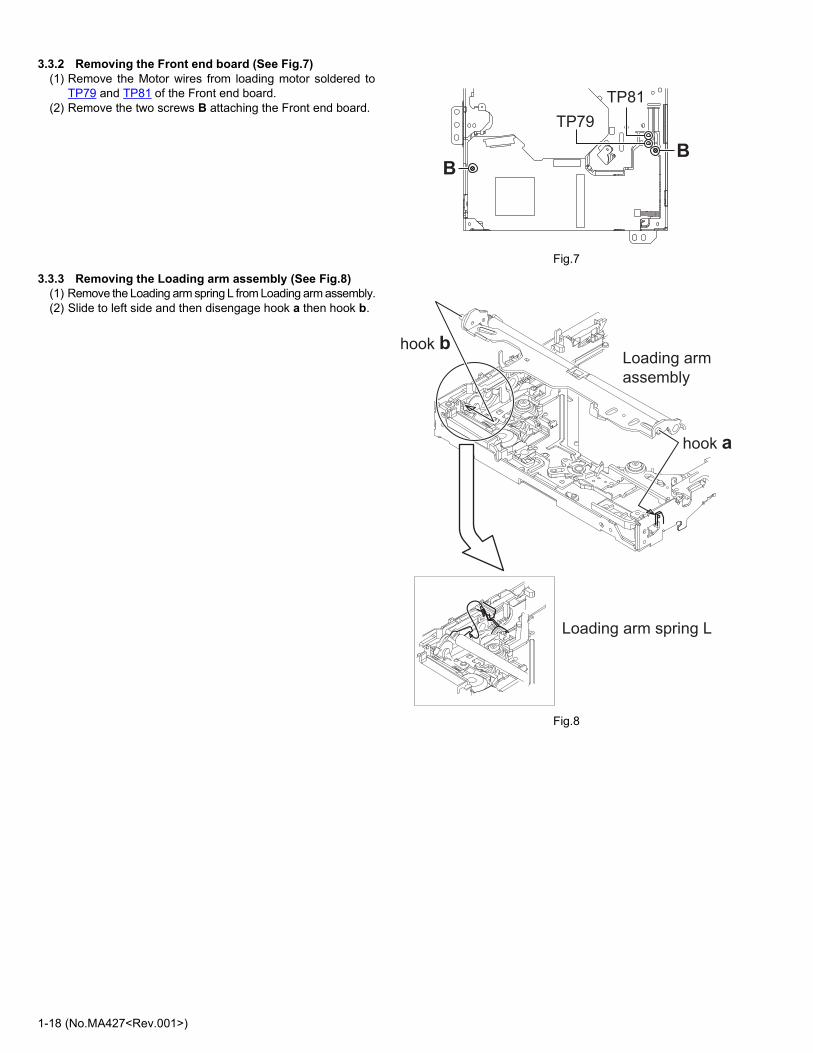
3.3.2 Removing the Front end board (See Fig.7)(1) Remove the Motor wires from loading motor soldered to
TP79 and TP81 of the Front end board.(2) Remove the two screws B attaching the Front end board.
Fig.7
3.3.3 Removing the Loading arm assembly (See Fig.8)(1) Remove the Loading arm spring L from Loading arm assembly.(2) Slide to left side and then disengage hook a then hook b.
Fig.8
BB
TP79
TP81
Loading armassembly
Loading arm spring L
hook a
hook b

(No.MA427<Rev.001>)1-19
3.3.4 Removing the Gear base assembly (See Fig.9, 10)(1) Remove the Loading arm spring L. (See Fig.9)(2) Remove the two screws C attaching the Gear base assembly.
(See Fig.10)
Fig.9
Fig.10
3.3.5 Removing the Loading arm holder. (See Fig.11)(1) Remove the two screws D attaching the Loading arm holder.(2) Remove the Loading arm spring R.
Fig.11
Loading armspring L
C
D
Loading arm
spring R
Loading arm
holder

1-20 (No.MA427<Rev.001>)
3.3.6 Removing the Loading moor assembly (See Fig.12)(1) Remove the three screws E attaching the Loading motor
assembly.
Fig.12
3.3.7 Removing the Slide cam assembly (See Fig.13)(1) Slide to backward the Slide cam assembly and the remove
the Slide cam spring.(2) Slide to frontward the slide cam assembly, and then take
out it.
Fig.13
3.3.8 Removing the Photo board (See Fig.14)(1) Pressing the hook c and then slide to backward (slide to the
arrow side) the Disc plate.(2) Remove the one screw F attaching the Photo board.
Fig.14
E
Slide cam assembly
Slide cam spring
hook c
hook c
F
Photo board

(No.MA427<Rev.001>)1-21
3.3.9 Removing the Loading motor (See Fig.15 to 18)(1) Remove the A wheel gear. (See Fig.15)(2) Remove the A worm gear, M connect gear and M wheel
gear by sequentially. (See Fig.16)(3) Remove the two screws G attaching the Loading motor.
(Se Fig.17)(4) When attaching the Loading motor, motor wire should arrange
to figure. (See Fig.18)
Fig.15
Fig.16
Fig.17
Fig.18
A Wheel gear
A worm gear
M connect gear
M wheel gear
G
Wire arrangement
1-22 (No.MA427<Rev.001>)
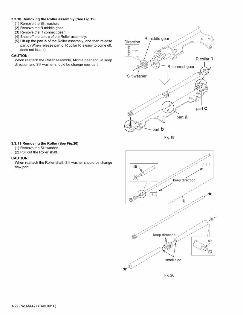
3.3.10 Removing the Roller assembly (See Fig.19)(1) Remove the Slit washer.(2) Remove the R middle gear.(3) Remove the R connect gear.(4) Snap off the part a of the Roller assembly.(5) Lift up the part b of the Roller assembly, and then release
part c (When release part c, R collar R is easy to come off,does not lose it).
CAUTION:When reattach the Roller assembly, Middle gear should keepdirection and Slit washer should be change new part.
Fig.19
3.3.11 Removing the Roller (See Fig.20)(1) Remove the Slit washer.(2) Pull out the Roller shaft.
CAUTION:When reattach the Roller shaft, Slit washer should be changenew part.
Fig.20
Direction
Slit washer
R connect gear
R collar R
R middle gear
part b
part a
part c
keep direction
slit
small side
keep directionslit

(No.MA427<Rev.001>)1-23
SECTION 4ADJUSTMENT
4.1 Test instruments required for adjustment(1) Digital oscilloscope (100MHz)(2) Digital tester(3) Test Disc (4) Extension cable : EXTXD002-60PF (CN881-CN503)
(CN602-CN403) : EXTDV001-30PF (CN982-CN605) : EXTLX001-4P (WR981-CN607) : EXTFP001-30P (CN981-CN802) : EXTFP001-12P (CN606-CN801) : EXTCN001-6P (CN961-CN851) : EXTJD001-14PF (CN983-CN653)
(5) Extension studs : STDV001-3P
4.2 Standard measuring conditionsLoad impedance 20K.(2 Speakers connection) Power supply voltage DC14.4V(10.5 to 16V) Output Level Line out 2.5V (Vol. MAX)
4.3 Standard volume positionBalance and Bass &Treble volume : lndication"0"Loudness : OFF
4.4 Dummy loadExclusive dummy load should be used for AM,and FM. For FM dummy load, there is a loss of 6dB between SSG outputand antenna input. The loss of 6dB need not be considered sincedirect reading offigures are applied in this working standard.
4.5 How to connect the extension cable for adjustingCaution:
Be sure to attach the heat sink and rear bracket onto the power amplifier IC and regulator IC respectively,before supply the power.If voltage is applied without attaching these parts, the power amplifier IC and regulator IC will be destroyed by heat.
EXTFP001-12P
EXTFP001-12P
EXTXD002-60PF
CN503
CN801
CN802
CN851
CN982CN982CN982
WR981
CN981
CN961
CN983CN983CN983
CN653
CN602CN605
CN607CN606
EXTCN001-6P
EXTJD001-14PFEXTJD001-14PFEXTJD001-14PF
EXTDV001-30PF
EXTDV001-30PFEXTXD002-60PFEXTXD002-60PFEXTXD002-60PF EXTXD002-60PF
EXTLX001-4P
EXTLX001-4PEXTLX001-4PEXTLX001-4P
EXTFP001-30P
EXTFP001-30P
EXTJD001-14PFExtension studs
STDV001-3P
CN403CN403CN403
CN881CN881CN881CN881CN881

1-24 (No.MA427<Rev.001>)
4.6 Service mode
Note :There is the function that is not displayed by a version.
4.6.1 Service mode 1 (Indication of a service mode 1 is nothing.)
[ Exit ][ Back ]
[ STAND BY / ON ATTENUATOR ] [ VOL ] [MAP ] [ OPEN ][ DISP ]
TOUCH PANELREW Button FF Button
UP Button
ENTER
DOWN Button
Keep this state more 2 seconds
while continuing pressing the
[STANDBY/ON ATTENUATOR] button
and [OPEN] button sequentially.
NO EJECT? *1
EMERGENCY EJECT *2
Exchanging it operate a menu of a service mode with the [UP] button
and [DOWN] button. Operate choice of a menu with a [ENTER] button.
*1 : When an [ENTER] button is pushed in NO EJECT indication, it is set
by an EJECT prohibition mode.
When an [ENTER] button is pushed in EJECT OK indication, it is aet
by a normal mode.
*2 : Forced EJECT movement
A screen becomes normal indication after an ENTER button was pushed.
Screen indication
(No.MA427<Rev.001>)1-25
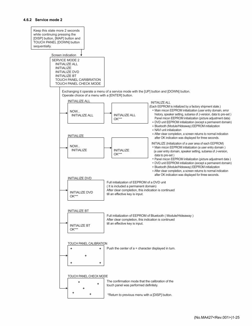
4.6.2 Service mode 2
Keep this state more 2 seconds
while continuing pressing the
[DISP] button, [MAP] button and
TOUCH PANEL [DOWN] button
sequentially.
SERVICE MODE 2
INITIALIZE ALL
INITIALIZE
INITIALIZE DVD
INITIALIZE BT
TOUCH PANEL CARIBRATION
TOUCH PANEL CHECK MODE
Screen indication
Exchanging it operate a menu of a service mode with the [UP] button and [DOWN] button.
Operate choice of a menu with a [ENTER] button.
INITIALIZE ALL
INITIALIZE
INITIALIZE DVD
INITIALIZE BT
TOUCH PANEL CALIBRATION
TOUCH PANEL CHECK MODE
NOW...
INITIALIZE ALL
NOW...
INITIALIZE
INITIALIZE DVD
OK***
INITIALIZE BT
OK***
INITIALIZE ALL
OK***
INITIALIZE
OK***
INITIALIZE (Initialization of a user area of each EEPROM)
Main micon EEPROM initialization (a user entry domain )
(a user entry domain, speaker setting, subarea of J-version,
data to pre-set )
Panel micon EEPROM initialization (picture adjustment data )
DVD unit EEPROM initialization (except a permanent domain)
Bluetooth (Module/Hideaway) EEPROM initialization
After clear completion, a screen returns to normal indication
after OK indication was displayed for three seconds.
INITIALIZE ALL
(Each EEPROM is initialized by a factory shipment state.)
Main micon EEPROM initialization (user entry domain, error
history, speaker setting, subarea of J-version, data to pre-set )
Panel micon EEPROM initialization (picture adjustment data)
DVD unit EEPROM initialization (except a permanent domain)
Bluetooth (Module/Hideaway) EEPROM initialization
NAVI unit initialization
After clear completion, a screen returns to normal indication
after OK indication was displayed for three seconds.
Full initialization of EEPROM of a DVD unit
( It is included a permanent domain)
After clear completion, this indication is continued
till an effective key is input.
Full initialization of EEPROM of Bluetooth ( Module/Hideaway )
After clear completion, this indication is continued
till an effective key is input.
Push the center of a + character displayed in turn.
The confirmation mode that the calibration of the
touch panel was performed definitely.
*Return to previous menu with a [DISP] button.
1-26 (No.MA427<Rev.001>)
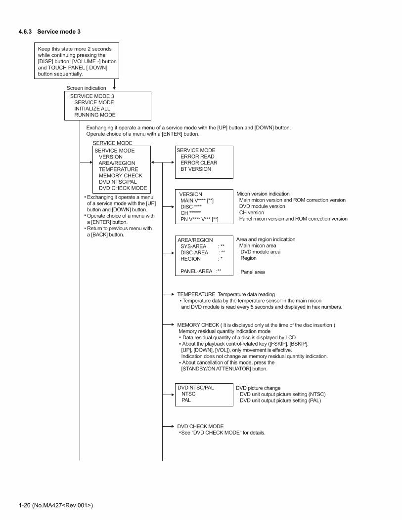
4.6.3 Service mode 3
Keep this state more 2 seconds
while continuing pressing the
[DISP] button, [VOLUME -] button
and TOUCH PANEL [ DOWN]
button sequentially.
SERVICE MODE 3
SERVICE MODE
INITIALIZE ALL
RUNNING MODE
Screen indication
Exchanging it operate a menu of a service mode with the [UP] button and [DOWN] button.
Operate choice of a menu with a [ENTER] button.
SERVICE MODE
SERVICE MODE
VERSION
AREA/REGION
TEMPERATURE
MEMORY CHECK
DVD NTSC/PAL
DVD CHECK MODE
Exchanging it operate a menu
of a service mode with the [UP]
button and [DOWN] button.
Operate choice of a menu with
a [ENTER] button.
Return to previous menu with
a [BACK] button.
SERVICE MODE
ERROR READ
ERROR CLEAR
BT VERSION
VERSION
MAIN V**** [**]
DISC ****
CH ******
PN V**** V*** [**]
AREA/REGION
SYS-AREA : **
DISC-AREA : **
REGION : *
PANEL-AREA :**
Micon version indication
Main micon version and ROM correction version
DVD module version
CH version
Panel micon version and ROM correction version
Area and region indicattion
Main micon area
DVD module area
Region
Panel area
TEMPERATURE Temperature data reading
Temperature data by the temperature sensor in the main micon
and DVD module is read every 5 seconds and displayed in hex numbers.
MEMORY CHECK ( It is displayed only at the time of the disc insertion )
Memory residual quantity indication mode
Data residual quantity of a disc is displayed by LCD.
About the playback control-related key ([FSKIP], [BSKIP],
[UP], [DOWN], [VOL]), only movement is effective.
Indication does not change as memory residual quantity indication.
About cancellation of this mode, press the
[STANDBY/ON ATTENUATOR] button.
DVD NTSC/PAL
NTSC
PAL
DVD picture change
DVD unit output picture setting (NTSC)
DVD unit output picture setting (PAL)
DVD CHECK MODE
See "DVD CHECK MODE" for details.

(No.MA427<Rev.001>)1-27
ERROR READ
DVD ERROR READ
CH ERROR READ
MECHA ERROR READ
NAVI ERROR READ
READ ALL
ERROR CLEAR
DVD ERROR CLEAR
CH ERROR CLEAR
MECHA ERROR CLEAR
NAVI ERROR CLEAR
BT VERSION
SW BT CORE ***
HW BT MODULE ***
SW BT MODULE ***
SW HIDEAWAY ***
ADR- ***********
NOW ...
INITIALIZE ALL INITIALIZE ALL
OK**
DVD ERROR READ
Reading of a DVD unit error history
CH ERROR READ
Reading of a CD changer error history
MECHA ERROR READ
Reading of a door mechanism error history
NAVI ERROR READ
Reading of a NAVI module error history
READ ALL
Reading of a main micon EEPROM (All contents)
Clear of each error history
A screen returns to following
indication after clear completion.
Bluetooth version indication
*It is displayed in Bluetooth unit connection.
Software version of BT core
Hardware version of BT Module
Software version of BT Module
Software version of BT Hideaway controller
BT Address
INITIALIZE ALL (Each EEPROM is initialized
by a factory shipment state.)
Main micon EEPROM initialization
(user entry domain, error history, speaker setting,
subarea of J-version, data to pre-set )
Panel micon EEPROM initialization
(picture adjustment data)
DVD unit EEPROM initialization
(except a permanent domain)
Bluetooth (Module/Hideaway)
EEPROM initialization
NAVI unit initialization
After clear completion, a screen returns to normal
indication after OK indication was displayed for
three seconds.
RUNNING MODE
See "Running mode" for details.

1-28 (No.MA427<Rev.001>)
4.6.4 Service mode 4
Keep this state more 2 seconds
while continuing pressing the
[DISP] button, [VOLUME +] button
and TOUCH PANEL [DOWN]
button sequentially.
SERVICE MODE 4
RDS S MODE
MONITOR S MODE
HD RADIO S MODE
Exchanging it operate s menu of a service mode with the [UP] button and [DOWN] button.
Operate choice of a menu with a [ENTER] button.
RDS S MODE
RDS service mode
MONITOR S MODE
R/W CHROMA
DATA CLEAR
*See "Monitor adjustment" for details.
CHROMA DATA read/write
Clear of CHROMA DATA (return to an initial value)
HD RADIO S MODE
It is displayed in HD Radio unit connection.

(No.MA427<Rev.001>)1-29
4.6.5 Service mode 9
Screen indication
Exchanging it operate a menu of a service mode with the [UP] button and [DOWN] button.
Operate choice of a menu with a [ENTER] button.
NAVI SERVICE MODE
Keep this state more 2 seconds
while continuing pressing the
[OPEN] button, [MAP] button
and TOUCH PANEL [DOWN]
button sequentially.
SERVICE MODE 9
NAVI SERVICE MODE
NAVI UPDATE MODE
Service Mode
Version
Sensor Test
Gyro Test
TMC Tuner Test
Voice Test
SD Slot Test
Service Mode
System Information
Sensor Status
TMC Status
System Error
Debug Mode
Edit System Files
Initialize
Version
SDK Version : *.*.**
APP Version : *.*.*.*
Map Version : *.*.*.*
GPS Version : *.*.*.*
Sensor Version : *.*.*.*
Unit Name : KW-NX7000(*)
Unit ID : 02********
Sensor Test
GPS-Sat :*/* Gyro Factor : -
Speed Pulse : -
Parking : **
Reverse : **
Illumination : **
Gyro Test : Only the factory use.
TMC Tuner Test
Searching Station...
Voice Test
Maximum Volume
Medium Volume
Minimum Volume
SD Slot Test : Only the factory use.

1-30 (No.MA427<Rev.001>)
System Information
SDK Version : *.*.**
APP Version : *.*.*.*
Map Version : *.*.*.*
GPS Version : *.*.*.*
Sensor Version : *.*.*.*
Unit Name : KW-NX7000(*)
Unit ID : 02********
Sensor Status
GPS-Sat : */*
GPS-HDOP : *.*
WAAS/EGNOS : **
GPS-Lat : N x xx'xx"
GPS-Lon : E x xx'xx"
GPS-Alt : x m
GPS-Speed : x km/h
TMC Status
Status :******* PI : ****
Freq : xxx.x MHz SID : **
S-Level : x dB LTN : **
Threshold : x dB CC : **
ECC : **
System Error
Total : ** E-1 : ****
E-2 : ****
E-3 : ***
Debug Mode
Off
Record Mode
Playback Mode
Edit System Files
Save All Log Files
Delete All Log Files
Write Serial Number
NAVI UPDATE MODE
(No.MA427<Rev.001>)1-31
4.7 write serial numberNote:
There is need to input a serial number into when changed NAVI PWB board with J version.(1) Set to Service Mode 9.(2) Choose an NAVI Service Mode.(3) Choose an Edit System Files.(4) Choose a Write Serial Number.(5) Input 8 columns of serial number.(6) Push OK.
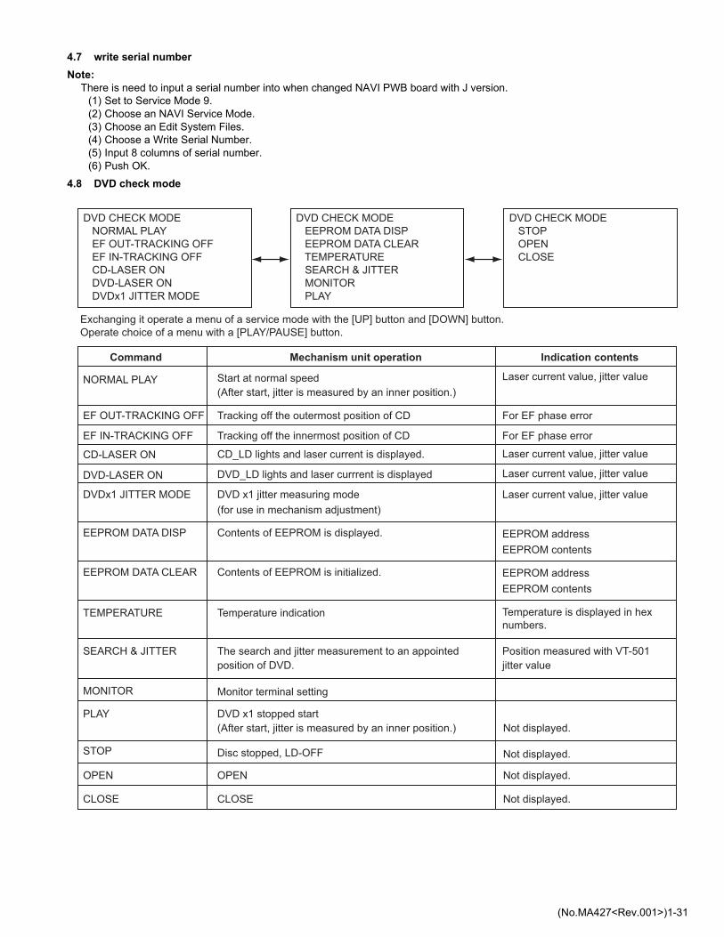
4.8 DVD check mode
DVD CHECK MODE
NORMAL PLAY
EF OUT-TRACKING OFF
EF IN-TRACKING OFF
CD-LASER ON
DVD-LASER ON
DVDx1 JITTER MODE
DVD CHECK MODE
EEPROM DATA DISP
EEPROM DATA CLEAR
TEMPERATURE
SEARCH & JITTER
MONITOR
PLAY
DVD CHECK MODE
STOP
OPEN
CLOSE
Exchanging it operate a menu of a service mode with the [UP] button and [DOWN] button.
Operate choice of a menu with a [PLAY/PAUSE] button.
Command Mechanism unit operation Indication contents
NORMAL PLAY Start at normal speed
(After start, jitter is measured by an inner position.)
Laser current value, jitter value
EF OUT-TRACKING OFF Tracking off the outermost position of CD For EF phase error
For EF phase error EF IN-TRACKING OFF Tracking off the innermost position of CD
CD-LASER ON
DVD-LASER ON
EEPROM DATA DISP
EEPROM DATA CLEAR
TEMPERATURE
SEARCH & JITTER
CD_LD lights and laser current is displayed.
DVD_LD lights and laser currrent is displayed
DVDx1 JITTER MODE DVD x1 jitter measuring mode
(for use in mechanism adjustment)
Laser current value, jitter value
Laser current value, jitter value
Laser current value, jitter value
Contents of EEPROM is displayed. EEPROM address
EEPROM contents
EEPROM address
EEPROM contents
Contents of EEPROM is initialized.
Temperature indication Temperature is displayed in hex
numbers.
The search and jitter measurement to an appointed
position of DVD.
Position measured with VT-501
jitter value
MONITOR Monitor terminal setting
PLAY DVD x1 stopped start
(After start, jitter is measured by an inner position.) Not displayed.
Not displayed.
Not displayed.
Not displayed.
STOP
OPEN
CLOSE CLOSE
Disc stopped, LD-OFF
OPEN

1-32 (No.MA427<Rev.001>)
4.9 Error code tables
Error contents Details Error code Detailed error code
TOC read error
First track access error
Last track access error
T1 access error
T12 access error
T24 access error
Read-in area read error
DVD L1 layer adjustment error
DVD L0 layer adjustment error
NO DISC judgment
It is NO DISC by start failure
It is stopped by playback inability.
Seek access error
Logic format NG
TOC lead movement of a CD is not completed.
Even if TOC reading passes after the end with CD running mode for 30 seconds, the first track access is not finished.
Even if first track passes after the end with CD running mode for 30 seconds, the last track access is not finished.
Even if T1 access passes in a DVD runnung mode for 30 seconds, it is not finished.
Even if T12 access passes in a DVD runnung mode for 30 seconds, it is not finished.
Even if T24 access passes in a DVD runnung mode for 30 seconds, it is not finished.
Disc error code
Read-in area read operation of DVD is not completed.
Adjustment of L1 layer of DVD is not finishhed normally. (including focus jump failure)
Adjustment of L0 layer of DVD is not finishhed normally. (including focus jump failure)
Judgment without disc
Start is impossible
Stop in running mode playback
Logic format analysis inability or non-correspondence logic format
It cannot arrive at an aim address even if it passes for 15 seconds.
84
84
80
80
80
80
80
80
80
80
80
80
80
80
0059
0060
0061
0069
0070
0071
0072
0074
0075
0090
0091
0093
0094
0095
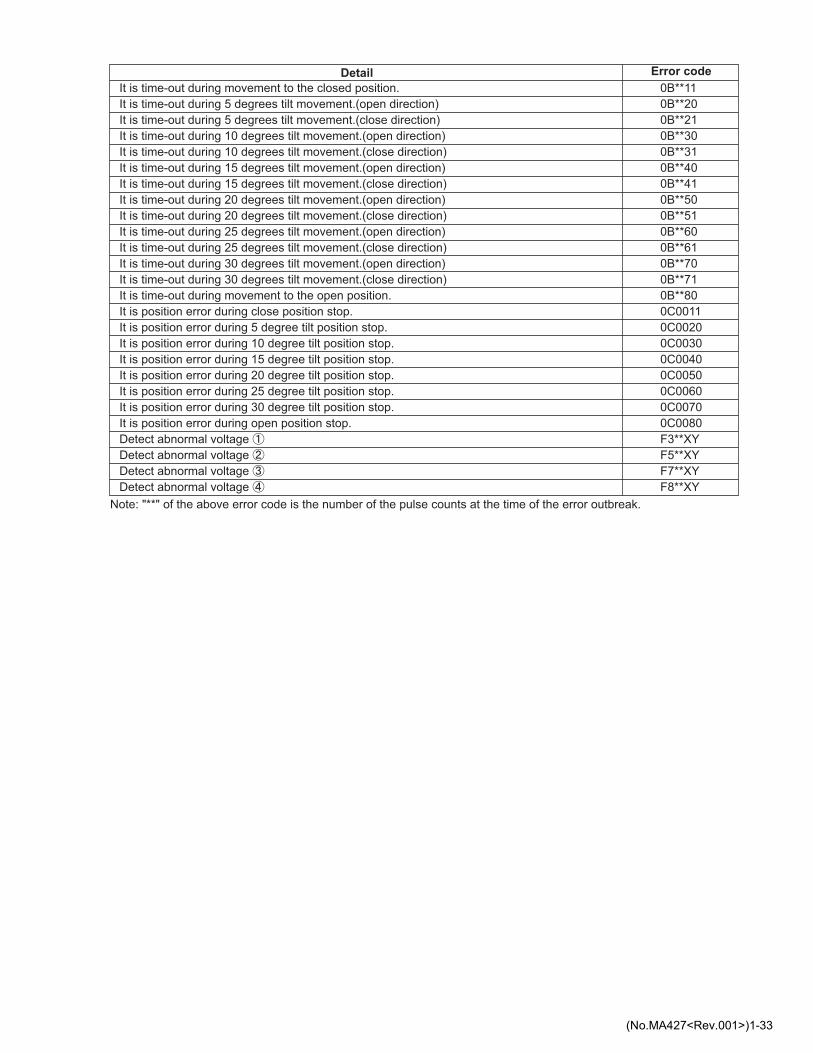
Error codes of panel mechanism * As for two columns of the beginning of the error code, as for error contents, two columns of middle, number of the pulse counts, last two columns are a purpose position and movement directions.
Error contents code
Time out OB
OC
F3
F5
F7
F8
Position error by the external force
When assumed last two columns XY;, as for X, as for purpose position,
Y, is a movement direction.
Purpose position
CLOSE
OPEN
5 degrees
10 degrees
15 degrees
20 degree
25 degrees
30 degrees
1
2
3
4
5
6
7
8
X Movement direction
Open direction
Close direction
Y
0
1
Error contents Details Error code Detailed error code
Error in loading wait Loading of a running mode Disc was pulled out in a wait.
09
09
Mechanism error code
0101
0013
00230024
0031
(No.MA427<Rev.001>)1-33
It is time-out during movement to the closed position.
It is time-out during 5 degrees tilt movement.(open direction)
It is time-out during 5 degrees tilt movement.(close direction)
It is time-out during 10 degrees tilt movement.(open direction)
It is time-out during 10 degrees tilt movement.(close direction)
It is time-out during 15 degrees tilt movement.(open direction)
It is time-out during 15 degrees tilt movement.(close direction)
It is time-out during 20 degrees tilt movement.(open direction)
It is time-out during 20 degrees tilt movement.(close direction)
It is time-out during 25 degrees tilt movement.(open direction)
It is time-out during 25 degrees tilt movement.(close direction)
It is time-out during 30 degrees tilt movement.(open direction)
It is time-out during 30 degrees tilt movement.(close direction)
It is time-out during movement to the open position.
It is position error during close position stop.
It is position error during 5 degree tilt position stop.
It is position error during 10 degree tilt position stop.
It is position error during 15 degree tilt position stop.
It is position error during 20 degree tilt position stop.
It is position error during 25 degree tilt position stop.
It is position error during 30 degree tilt position stop.
It is position error during open position stop.
Detect abnormal voltage
Detect abnormal voltage
Detect abnormal voltage
Detect abnormal voltage
0B**11
0B**20
0B**21
0B**30
0B**31
0B**40
0B**41
0B**50
0B**51
0B**60
0B**61
0B**70
0B**71
0B**80
0C0011
0C0020
0C0030
0C0040
0C0050
0C0060
0C0070
0C0080
F3**XY
F5**XY
F7**XY
F8**XY
Detail Error code
Note: "**" of the above error code is the number of the pulse counts at the time of the error outbreak.

1-34 (No.MA427<Rev.001>)
4.10 Running mode
Panel close Panel open
Panel close 5 degrees 10 degrees 15 degrees 20 degrees
25 degrees 30 degrees Panel open
Panel close 5 degrees 30 degrees 5 degrees Panel close
Loading Eject Wait for 5 seconds+Door open/close
Loading Eject Wait for 5 seconds+Door open/close
Loading Playback Eject Wait for 5 seconds+Door open/close
Loading Playback Eject Wait for 5 seconds+Door open/close
Loading Playback Eject Wait for 5 seconds+Door open/close
Loading Playback Eject Wait for 5 seconds+Door open/close
RUNNING1 MECHA
RUNNING2 MECHA
RUNNING 3 MECHA
RUNNING4 DVD
RUNNING5 DVD
RUNNING6 DVD
RUNNING7 DVD
RUNNING8 DVD
RUNNING9 DVD
Door mecha running 1
Door mecha running 2
Door mecha running 3
DVD+Door mecha running1
DVD+Door mecha running2
DVD+Door mecha running3
DVD+Door mecha running4
DVD+Door mecha running5
DVD+Door mecha running6
In mecha error In disc errorIndication Explanation Operation contents of 1 cycle
-
-
-
Stop
Retry
Stop
Retry
Stop
Retry
-
-
-
-
-
Stop
Stop
Retry
Retry
* Cancellation of running1,2 and 3 : Press the [EJECT] key * In running 1,2 and 3 cancellation, a door does not stop at the position and moves to a panel position. * Cancellation of running4 to 9 : Press the [POWER] key* The number of count and an error cord are displayed in running.
Playback contents in a running mode
CD
The first track is played for 30 seconds. The last track is played for 30 seconds.
(The last track is played in the case of less than till the last for 30 seconds.)
DVD
2layer disc (Pit disc)
Title 1 (the L0 layer internal circumference) is played for 30 seconds.
Title 12 (L0 layer circumference) is played for 30 seconds.
Title 24 (L1layer internal circumference) is played for 30 seconds.
2layer disc (Recordable disc)
Title 1 (the L0 layer internal circumference) is played for 30 seconds.
Title 13 (L0 layer circumference) is played for 30 seconds.
Title 24 (L1layer internal circumference) is played for 30 seconds.
1layer disc
First chapter of title 1 is played for 30 seconds. The last chapter of title 1 is played for 30 seconds.

(No.MA427<Rev.001>)1-35
4.11 Monitor adjustment
00001
00002
00003
00004
00005
00006
00007
00008
00009
00010
00011
00012
00013
00014
00015
00016
00017
00018
00019
00020
00021
00022
00023
00024
00025
00026
00027
00028
00029
00030
00031
00032
00033
00034
00035
00036
00037
00038
00039
00040
00041
00042
00043
00044
00045
00046
00047
00048
00049
00050
00051
00052
00053
00054
00055
00000
00000
00000
00000
00000
00000
00000
00000
00000
00000
00000
00000
00000
00000
00000
00000
00000
00000
00000
00000
00000
00000
00000
00000
00000
00000
00000
00000
00000
00000
00000
00000
00000
00000
00000
00000
00000
00000
00000
00000
00000
00000
00000
00000
00000
00000
00000
00000
00000
00000
00000
00000
00000
00000
00000
00001
00003
00063
00003
00063
00001
00001
00511
00511
00255
00255
00255
00255
00255
00255
00003
00003
00127
00127
00006
00006
00255
00255
00255
00255
00255
00255
00255
00255
00511
00511
00001
00255
01023
01023
00511
00255
00255
00255
00511
00001
00001
00127
00127
00127
00127
00127
00127
00127
00127
00127
00127
00127
00127
00127
00000
00000
00000
00000
00000
00000
00000
00000
00000
00128
00128
00064
00068
00000
00000
00001
00001
00000
00000
00000
00000
00125
00125
00090
00100
00131
00131
00051
00051
00094
00094
00000
00016
00320
00322
00348
00210
00210
00158
00267
00001
00001
00029
00028
00058
00059
00057
00059
00054
00053
00061
00061
00061
00061
00061
00000
00000
00000
00000
00000
00000
00000
00000
00000
00128
00128
00064
00068
00000
00000
00001
00001
00000
00000
00000
00000
00125
00125
00090
00100
00131
00131
00051
00051
00094
00094
00000
00016
00320
00322
00348
00210
00210
00158
00267
00001
00001
00029
00028
00058
00057
00057
00056
00054
00053
00061
00061
00061
00061
00061
Fix
Fix
Fix
Fix
Fix
Fix
Fix
Fix
Fix
Adjust
Adjust
Adjust
Adjust
Adjust
Adjust
Adjust
Adjust
Adjust
Adjust
Adjust
Adjust
Fix
Fix
Fix
Fix
Adjust
Adjust
Adjust
Adjust
Fix
Fix
Fix
Fix
Adjust
Adjust
Fix
Fix
Fix
Fix
Fix
Fix
Fix
Adjust
Adjust
Fix
Fix
Fix
Fix
Fix
Fix
Fix
Fix
Fix
Fix
Fix
Color amplitude revision ON/OFF
Color amplitude revision CAS
Color amplitude revision APC
Color amplitude revision CUS
Color amplitude revision APU
Black level extension ON/OFF
Black level extension FUNCTION
Black level extension START POINT
Black level extension OFFSET
Enhancer revision effect adjustment (NTSC)
Enhancer revision effect adjustment (PAL)
Limiter of the horizontal enhancer (NTSC)
Limiter of the horizontal enhancer (PAL)
Filter choice of the horizontal enhancer (NTSC)
Filter choice of the horizontal enhancer (PAL)
Tap change of the brightness outline revision (NTSC)
Tap change of the brightness outline revision (PAL)
Adjustment of the quantity of brightness outline core ring (NTSC)
Adjustment of the quantity of brightness outline core ring (PAL)
Adjustment of the brightness outline revision gain (NTSC)
Adjustment of the brightness outline revision gain (PAL)
Change in TINT of the whole picture (NTSC)
Change in TINT of the whole picture (PAL)
Change with the deepness of the color of the whole picture (NTSC)
Change with the deepness of the color of the whole picture (PAL)
Tint adjustment (NTSC)
Tint adjustment (PAL)
Color adjustment (NTSC)
Color adjustment (PAL)
Set the offset DC of the input video signal (NTSC)
Set the offset DC of the input video signal (PAL)
Quantity of transmission revision of the YUV DC
Quantity of transmission revision of the YUV DC
Contrast adjustment between the black - white (NTSC)
Contrast adjustment between the black - white (PAL)
Conversion coefficients from YUV to RGB (PRCL)
Conversion coefficients from YUV to RGB (PBCL)
Conversion coefficients from YUV to RGB (YCL)
Conversion coefficients from YUV to RGB (BCL)
Conversion coefficients from YUV to RGB (RCL)
Noise shaving (NTSC)
Noise shaving (PAL)
Black level adjustment (NTSC)
Black level adjustment (PAL)
Gain setting of Red signal (NTSC)
Gain setting of Red signal (PAL)
Gain setting of Green signal (NTSC)
Gain setting of Green signal (PAL)
Gain setting of Blue signal (NTSC)
Gain setting of Blue signal (PAL)
Set the cut-off of the Red signal (NTSC)
Set the cut-off of the Red signal (PAL)
Set the cut-off of the Green signal (NTSC)
Set the cut-off of the Green signal (PAL)
Set the cut-off of the Blue signal (NTSC)
Indication Minimum value Maximum value Initial value DetailReference register value
* When adjusting, switch on the main unit and insert a test disc (VT-501). And play the test disc and pause it.
1. Set the service mode 4.
2. Exchanging it operate a menu of a service mode with the [UP] button and [DOWN] button.
3. Change data with the [B.SKIP]/[F.SKIP] buttons.
4. Write data with a [ENTER] button.

1-36 (No.MA427<Rev.001>)
Indication Minimum value Maximum value Initial value DetailReference register value
00056
00057
00058
00059
00060
00061
00062
00063
00064
00065
00066
00067
00068
00069
00070
00071
00072
00073
00074
00075
00076
00077
00078
00079
00080
00081
00082
00083
00084
00085
00086
00087
00088
00089
00090
00091
00092
00093
00094
00095
00096
00097
00098
00099
00100
00101
00102
00103
00104
00105
00106
00107
00108
00109
00110
00111
00112
00113
00114
00115
00116
00117
00118
00119
00120
00000
00000
00000
00000
00000
00000
00000
00000
00000
00000
00000
00000
00000
00000
00000
00000
00000
00000
00000
00000
00000
00000
00000
00000
00000
00000
00000
00000
00000
00000
00000
00000
00000
00000
00000
00000
00000
00000
00000
00000
00000
00000
00000
00000
00000
00000
00000
00000
00000
00000
00000
00000
00000
00000
00000
00000
00000
00000
00000
00000
00000
00000
00000
00000
00000
00127
00001
00255
00255
00255
00255
00255
00255
00255
00255
00255
00255
00255
00255
00255
00255
00255
00255
00255
00255
00255
00255
00255
00255
00255
00255
00255
00255
00255
00255
00255
00255
00255
00255
00255
00255
00255
00255
00255
00255
00255
00255
00255
00255
00255
00255
00255
00255
00255
00255
00255
00127
00127
00007
00007
00003
00003
00007
00007
00007
00007
01023
01023
00063
00063
00061
00001
00007
00015
00023
00031
00039
00047
00055
00017
00031
00032
00032
00036
00042
00058
00088
00007
00015
00023
00031
00039
00047
00055
00017
00031
00032
00032
00036
00042
00058
00088
00007
00015
00023
00031
00039
00047
00055
00017
00031
00032
00032
00036
00042
00058
00088
00060
00060
00010
00010
00042
00042
00001
00001
00032
00048
00000
00000
00001
00004
00180
00180
00001
00001
Fix
Fix
Fix
Fix
Fix
Fix
Fix
Fix
Fix
Fix
Fix
Fix
Fix
Fix
Fix
Fix
Fix
Fix
Fix
Fix
Fix
Fix
Fix
Fix
Fix
Fix
Fix
Fix
Fix
Fix
Fix
Fix
Fix
Fix
Fix
Fix
Fix
Fix
Fix
Fix
Fix
Fix
Fix
Fix
Fix
Fix
Fix
Adjust
Adjust
Adjust
Adjust
Fix
Fix
Fix
Fix
Fix
Fix
Fix
Fix
Adjust
Adjust
Fix
Fix
Adjust
Adjust
Set the cut-off of the Blue signal (PAL)
ON/OFF change of the gamma revision
Adjust 1 gamma revision point position of a Red signal
Adjust 2 gamma revision point position of a Red signal
Adjust 3 gamma revision point position of a Red signal
Adjust 4 gamma revision point position of a Red signal
Adjust 5 gamma revision point position of a Red signal
Adjust 6 gamma revision point position of a Red signal
Adjust 7 gamma revision point position of a Red signal
Appoint gamma revision gain 1 of the Red signal
Appoint gamma revision gain 2 of the Red signal
Appoint gamma revision gain 3 of the Red signal
Appoint gamma revision gain 4 of the Red signal
Appoint gamma revision gain 5 of the Red signal
Appoint gamma revision gain 6 of the Red signal
Appoint gamma revision gain 7 of the Red signal
Appoint gamma revision gain 8 of the Red signal
Adjust 1 gamma revision point position of a Green signal
Adjust 2 gamma revision point position of a Green signal
Adjust 3 gamma revision point position of a Green signal
Adjust 4 gamma revision point position of a Green signal
Adjust 5 gamma revision point position of a Green signal
Adjust 6 gamma revision point position of a Green signal
Adjust 7 gamma revision point position of a Green signal
Appoint gamma revision gain 1 of the Green signal
Appoint gamma revision gain 2 of the Green signal
Appoint gamma revision gain 3 of the Green signal
Appoint gamma revision gain 4 of the Green signal
Appoint gamma revision gain 5 of the Green signal
Appoint gamma revision gain 6 of the Green signal
Appoint gamma revision gain 7 of the Green signal
Appoint gamma revision gain 8 of the Green signal
Adjust 1 gamma revision point position of a Blue signal
Adjust 2 gamma revision point position of a Blue signal
Adjust 3 gamma revision point position of a Blue signal
Adjust 4 gamma revision point position of a Blue signal
Adjust 5 gamma revision point position of a Blue signal
Adjust 6 gamma revision point position of a Blue signal
Adjust 7 gamma revision point position of a Blue signal
Appoint gamma revision gain 1 of the Blue signal
Appoint gamma revision gain 2 of the Blue signal
Appoint gamma revision gain 3 of the Blue signal
Appoint gamma revision gain 4 of the Blue signal
Appoint gamma revision gain 5 of the Blue signal
Appoint gamma revision gain 6 of the Blue signal
Appoint gamma revision gain 7 of the Blue signal
Appoint gamma revision gain 8 of the Blue signal
Adjust the horizontal indication point of the picture (NTSC)
Adjust the horizontal indication point of the picture (PAL)
Adjust the vertical indication point of the picture (NTSC)
Adjust the vertical indication point of the picture (PAL)
AD clock gain adjustment (NTSC)
AD clock gain adjustment (PAL)
Noise reduction of the Y signal (NTSC)
Noise reduction of the Y signal (PAL)
Choose a YC separation filter (NTSC)
Choose a YC separation filter (PAL)
Color pulling out filter setting (NTSC)
Color pulling out filter setting (PAL)
Choose com movement mode and color BPF (NTSC)
Choose com movement mode and color BPF (PAL)
Vertical dot cancellation setting (NTSC)
Vertical dot cancellation setting (PAL)
Noise reduction setting (NTSC)
Noise reduction setting (PAL)

(No.MA427<Rev.001>)1-37
Indication Minimum value Maximum value Initial value DetailReference register value
00125
00126
00127
00128
00129
00130
00131
00132
00133
00134
00135
00136
00137
00138
00139
00140
00141
00142
00143
00144
00145
00146
00147
00148
00149
00150
00151
00152
00153
00154
00155
00156
00157
00158
00159
00160
00161
00162
00163
00164
00165
00121
00122
00123
00124
00000
00000
00000
00000
00000
00000
00000
00000
00000
00000
00000
00000
00000
00000
00000
00000
00000
00000
00000
00000
00000
00000
00000
00000
00000
00000
00000
00000
00000
00000
00000
00000
00000
00000
00000
00000
00000
00040
00040
00000
00000
00000
00000
00000
00000
00511
00511
00006
00255
00255
16383
16383
00127
00015
00063
00063
65535
65535
00063
00015
00015
00015
00015
00255
00255
00511
00511
00511
00026
00026
00255
00255
00255
00255
00255
00255
00255
00255
00255
00255
00009
00009
00110
00110
00007
00007
01023
01023
00255
00255
00140
00096
00004
00033
00033
02464
02472
00071
00015
00049
00049
14976
14976
00055
00010
00007
00001
00001
00252
00252
00326
00082
00033
00000
00000
00128
00000
00128
00000
00018
00023
00105
00104
00051
00051
00004
00006
00090
00060
00000
00000
00338
00338
00168
00168
00140
00096
00004
00033
00033
02464
02472
00071
00015
00049
00049
14976
14976
00055
00010
00007
00001
00001
00252
00252
00326
00082
00033
00000
00000
00128
00000
00128
00000
00018
00023
00098
00096
00051
00051
00004
00006
00090
00060
00000
00000
00338
00338
00168
00168
Adjust
Adjust
Fix
Fix
Fix
Fix
Fix
Fix
Fix
Fix
Fix
Fix
Fix
Fix
Fix
Fix
Fix
Fix
Fix
Fix
Fix
Fix
Fix
Fix
Fix
Fix
Fix
Fix
Fix
Adjust
Adjust
Adjust
Adjust
Adjust
Adjust
Fix
Fix
Fix
Fix
Fix
Fix
Fix
Fix
Fix
Fix
Color signal output level setting (NTSC)
Color signal output level setting (PAL)
ACC movement mode setting
C signal filter characteristic setting of the Y/C separation part (NTSC)
C signal filter characteristic setting of the Y/C separation part (PAL)
Amplitude killer off level setting
Amplitude killer on level setting
Clamp DC level adjustment setting
Clamp speed adjustment setting
Noise filter band setting of horizontal synchronization
signal and vertical synchronizing signal (NTSC)
Noise filter band setting of horizontal synchronization
signal and vertical synchronizing signal (PAL)
Horizontal phase comparison gain setting (NTSC)
Horizontal phase comparison gain setting (PAL)
Horizontal loop filter setting 1
Horizontal loop filter setting 2
Horizontal loop filter setting 3
Synchronization separation burst clock setting (NTSC)
Synchronization separation burst clock setting (PAL)
Free run center value setting of horizontal synchronization signal (NTSC)
Free run center value setting of horizontal synchronization signal (PAL)
DOKIDET 01
DOKIDET 02
DOKIDET 03
Unused
Unused
Subcareer center frequency setting (NTSC)
Unused
Subcareer center frequency setting (PAL)
Unused
Coordinate the delay of the C signal with a Y signal (NTSC)
Coordinate the delay of the C signal with a Y signal (PAL)
Coordinate the VCOM amplitude of the LCD (NTSC)
Coordinate the VCOM amplitude of the LCD (PAL)
Coordinate VCOM center value of the LCD (NTSC)
Coordinate VCOM center value of the LCD (PAL)
Set a variable range of the indication VSYNC frequency (NTSC)
Set a variable range of the indication VSYNC frequency (PAL)
Set time when indication VSYNC frequency changes (NTSC)
Set time when indication VSYNC frequency changes (PAL)
CLAMP MODE (NTSC)
CLAMP MODE (PAL)
Quantity of brightness adjustment setting (NTSC)
Quantity of brightness adjustment setting (PAL)
Brightness gain adjustment (NTSC)
Brightness gain adjustment (PAL)

1-38 (No.MA427<Rev.001>)
SECTION 5TROUBLESHOOTING
5.1 16 PIN CORD DIAGRAM (for J)
YL
BK
RD
BR
OR/WH
BL/WH
YG
BL
3
1
5
16
7
4
15
14
13
GN/BK
8
VI/BK6
WH9
8
7
6
5
16
15
14
134
3
2
1
12
11
10
9
BK
RD
WHGN
VI GY
BL/WH
GN/BK
VI/BK GY/BK
YL
BL
WH/BK
BR
YG
OR/WH
VI
GN
10 WH/BK
BK
RD
BL
WH
VI
Black
Red
Blue
White
Violet
GN
BR Brown
GY Gray
YL Yellow
Green
YG YellowGreen
OR Orange
GY
GY/BK
12
11
2

(No.MA427<Rev.001>)1-39
5.2 16 PIN CORD DIAGRAM (for E, EE)
8765
161514
1343
21
1211109
BK
RD
WHGN
VI GY
BL/WH
GN/BK
VI/BK GY/BK
YL
NC
WH/BK
BR
YG
OR/WH
BKRDBLWHVI
BlackRedBlueWhiteViolet
GN
BR BrownGY Gray
YL YellowGreen
YG YellowGreenOR Orange
1357
2468
NC YL
RD BK
NC BR
OR/WHBL/WH
135
7
2468
VI
GY
WH
GN
VI/BK
GY/BK
WH/BK
GN/BK
RD1
YL2
BK
BL/WH
OR/WH
RD3 RD2
YL1
YG
7
8
5
4
2
16
1
3
14
7
1
5
6
3
8
2
4
15
11
12
10
9
6
5
7
8
2
6
GY/BK
GY
WH/BK
WH
VI/BK
VI
GN/BK
GN
13 BR

(No.MA427<Rev.001>)
VPTPrinted in Japan
Victor Company of Japan, LimitedMobile Entertainment Division 10-1,1chome,Ohwatari-machi,Maebashi-city,371-8543,Japan

3-1
PARTS LIST
* All printed circuit boards and its assemblies are not available as service parts.
- Contents -
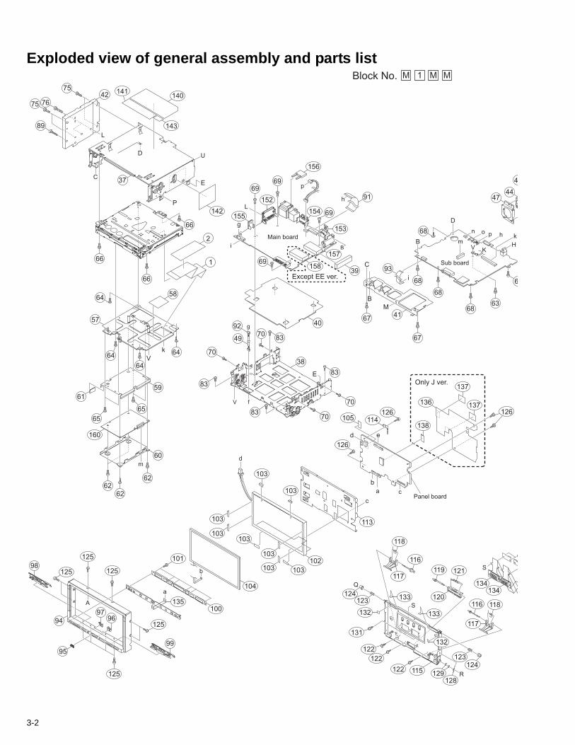
Exploded view of general assembly and parts list (Block No.M1)
DVD mechanism assembly and parts list (Block No.MJ)
Electrical parts list (Block No.01~05)
Packing materials and accessories parts list (Block No.M3)
KW-NX7000J,KW-NX7000E,KW-NX7000EE
3- 23- 83-103-26
MA427PAR<Rev.001>
3-2
Exploded view of general assembly and parts listBlock No. M MM1
b
A
a
m
k
V
c
d
Panel board
b
a c
Only J ver.
d e
i
k
Sub board
pon
H
hm
VB
B
M
C
D
f
g
V
B
Main board
g
h
p
i
E
L
R
Q
S
S
U
C
D
E
L
P
Except EE ver.
K
98
99
9697
103
103
140
104
102
113
128
105 114126
136
126
141
143
142
103
103
103
103
103
103
68
93
6863
68
67
67
68 6
41
44
4
47
100
101
37
75
7675
89
42
2
1
66
66
66
95
94
58
57
64
6262
62
6464
64
65
65
59
60
61
6969
69
156
91
7083
83
40
39
70
70
92
49
70
38
83
83 137
137
138
125
125
135
132
133
133
154
157
158
118
119 121
118
116
116
126
125
125
132
117
125
117
122 115 129
134134
122
123
123
124
124
122
131
120
152
153
155
69
160

3-3
MM
The parts without symbol number are not service.
Only J ver.
Only J ver.
A
nel board
nly J ver.
Connectionboard
e
R
k
Sub board
pon
H
hm
V
D
n
H
I
G
U
J I
J
o
K
R
S
qr
Front board
M
T
P
Q
q
rT
K
f
V
G
32
6
32
130130
128
36
145
112
107
110
109
106
112112
112
111
10822
27
25
34
35 21
24
90
19
7473
7473
8
6863
68
68
77
85
82
8277
84 77
77
77
7779
88
80
80
86
78
81
44
4845
47
46
43
53
30
72
72
51
71
71
72
72
50
8787
12
5
36
8
5
5
26
6
54
23
4
6
20
1112
4
10
4
311
9
31
7
29
14
17
18
15
14
17
16
13
3335
28
52
5654
55
137
137
38
132
133
118
119 121
116
127
127127
126
117
139
129
134134
123124
120
150
150
149
149
146
146151
147
147
151
148
144
159

3-4
General AssemblyBlock No. [M][1][M][M]
Symbol No. Part No. Part Name Description Local
1 QUQU05-6014AF-E FFC WIRE 60pin 14cm 2 LV44494-005A PROTECT SHEET 3 LV22458-002A B CHASSIS ASSY 4 LV44666-003A ROLLER(SLD) (x4) 5 QYWFM315013 WASHER 5mm/3.1mm x 0.13mm(x4) 6 QYWDL164035 SLIT WASHER 4mm/1.6mm x 0.35mm(x4) 7 LV36940-002A RAIL GUIDE (x2) 8 LV37308-001A GUIDE SPRING(L) 9 LV37309-001A GUIDE SPRING(R) 10 LV40846-053A SPACER(F) 11 QYSPSFT1745ZA TAP SCREW M1.7 x 4.5mm(x2) 12 QYSPSFT1745ZA TAP SCREW M1.7 x 4.5mm(x2) 13 LV36514-009A DRIVE PLATE ASS 14 LV44453-004A FRICTION SPRING (x2) 15 LV36516-001A RACK GEAR 16 LV36517-003A PHOTO PLATE 17 LV44159-004A MINI SCREW (x2) 18 LV44159-004A MINI SCREW (x3) 19 LV44159-004A MINI SCREW (x2) 20 LV36509-002A D.CHASSIS ASSY 21 QAR0378-001 MOTOR 22 WJM0460-001A-E E-SI C WIRE C-F 23 QYWFM265013 WASHER 5mm/2.6mm x 0.13mm(x3) 24 LV44451-001A WORM GEAR 25 LV36511-001A SECOND GEAR 26 LV36512-001A THIRD GEAR 27 LV36513-001A FORTH GEAR 28 QYWDM215025 SLIT WASHER 5mm/2.1mm x 0.25mm(x3) 29 LV44452-001A SPRING(WORM) 30 QYSPSPT2020ZA SCREW M2 x 2mm(x2) 31 LV44159-004A MINI SCREW 32 LV44615-001A SPECIAL SCREW (x3) 33 LV40846-057A SPACER (F) 34 LV36545-001A PCB BKT 35 LV44159-004A MINI SCREW (x3) 36 LV44159-004A MINI SCREW (x2) 37 LV11516-004A TOP CHASSIS 38 LV11517-002A MID CHASSIS 39 LV44247-006A SHIELD TIGHT 40 LV37302-003A INSULATOR 41 LV22633-002A FRONT PCB BKT 42 LV37304-005A SIDE HEAT SINK 43 LV22636-004A REAR BKT 44 QAR0455-001 COOLING FAN 45 LV40847-002A SPACER 46 LV37305-001A REAR HEAT SINK 47 LV37313-001A FAN BKT(IN) 48 LV37314-002A FAN BKT(OUT) 49 LV40847-016A SPACER (H) 50 LV22644-014A F CHASSIS ASSY J 50 LV22644-013A F CHASSIS ASSY E,EE 51 LV45134-002A BLIND 52 LV22638-002A FPC GUIDE 53 QYSDST2006MA TAP SCREW M2 x 6mm(x3) 54 LV37928-002A SD COVER 55 LV45081-001A SPECIAL SCREW (x2) 56 QYWDL164035 SLIT WASHER 4mm/1.6mm x 0.35mm(x2) 57 LV37927-001A CPU BKT ASSY 58 LV40847-049A SPACER(H) 59 LV22635-001A NAVI SHIELD TOP 60 LV22634-001A NAVI SHIELD BOT 61 LV44247-008A SHIELD TIGHT 62 LV44615-001A SPECIAL SCREW (x4) 63 LV44615-001A SPECIAL SCREW 64 LV44615-001A SPECIAL SCREW (x4) 65 LV44615-001A SPECIAL SCREW (x4) 66 LV44800-004A SPECIAL SCREW (x3) 67 LV44615-001A SPECIAL SCREW (x2) 68 LV44615-001A SPECIAL SCREW (x5) 69 LV44615-001A SPECIAL SCREW (x4) 70 LV41200-004A SPECIAL SCREW (x4) 71 LV44615-001A SPECIAL SCREW (x2) 72 LV43819-003A SPECAL SCREW (x4) 73 LV44470-002A SPECIAL SCREW (x2)
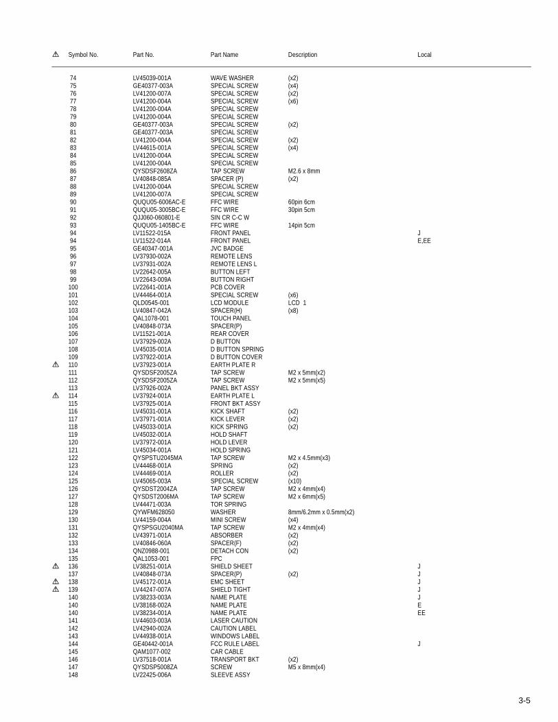
3-5
74 LV45039-001A WAVE WASHER (x2) 75 GE40377-003A SPECIAL SCREW (x4) 76 LV41200-007A SPECIAL SCREW (x2) 77 LV41200-004A SPECIAL SCREW (x6) 78 LV41200-004A SPECIAL SCREW 79 LV41200-004A SPECIAL SCREW 80 GE40377-003A SPECIAL SCREW (x2) 81 GE40377-003A SPECIAL SCREW 82 LV41200-004A SPECIAL SCREW (x2) 83 LV44615-001A SPECIAL SCREW (x4) 84 LV41200-004A SPECIAL SCREW 85 LV41200-004A SPECIAL SCREW 86 QYSDSF2608ZA TAP SCREW M2.6 x 8mm 87 LV40848-085A SPACER (P) (x2) 88 LV41200-004A SPECIAL SCREW 89 LV41200-007A SPECIAL SCREW 90 QUQU05-6006AC-E FFC WIRE 60pin 6cm 91 QUQU05-3005BC-E FFC WIRE 30pin 5cm 92 QJJ060-060801-E SIN CR C-C W 93 QUQU05-1405BC-E FFC WIRE 14pin 5cm 94 LV11522-015A FRONT PANEL J 94 LV11522-014A FRONT PANEL E,EE 95 GE40347-001A JVC BADGE 96 LV37930-002A REMOTE LENS 97 LV37931-002A REMOTE LENS L 98 LV22642-005A BUTTON LEFT 99 LV22643-009A BUTTON RIGHT100 LV22641-001A PCB COVER101 LV44464-001A SPECIAL SCREW (x6)102 QLD0545-001 LCD MODULE LCD 1103 LV40847-042A SPACER(H) (x8)104 QAL1078-001 TOUCH PANEL105 LV40848-073A SPACER(P)106 LV11521-001A REAR COVER107 LV37929-002A D BUTTON108 LV45035-001A D BUTTON SPRING109 LV37922-001A D BUTTON COVER
110 LV37923-001A EARTH PLATE R111 QYSDSF2005ZA TAP SCREW M2 x 5mm(x2)112 QYSDSF2005ZA TAP SCREW M2 x 5mm(x5)113 LV37926-002A PANEL BKT ASSY
114 LV37924-001A EARTH PLATE L115 LV37925-001A FRONT BKT ASSY116 LV45031-001A KICK SHAFT (x2)117 LV37971-001A KICK LEVER (x2)118 LV45033-001A KICK SPRING (x2)119 LV45032-001A HOLD SHAFT120 LV37972-001A HOLD LEVER121 LV45034-001A HOLD SPRING122 QYSPSTU2045MA TAP SCREW M2 x 4.5mm(x3)123 LV44468-001A SPRING (x2)124 LV44469-001A ROLLER (x2)125 LV45065-003A SPECIAL SCREW (x10)126 QYSDST2004ZA TAP SCREW M2 x 4mm(x4)127 QYSDST2006MA TAP SCREW M2 x 6mm(x5)128 LV44471-003A TOR SPRING129 QYWFM628050 WASHER 8mm/6.2mm x 0.5mm(x2)130 LV44159-004A MINI SCREW (x4)131 QYSPSGU2040MA TAP SCREW M2 x 4mm(x4)132 LV43971-001A ABSORBER (x2)133 LV40846-060A SPACER(F) (x2)134 QNZ0988-001 DETACH CON (x2)135 QAL1053-001 FPC
136 LV38251-001A SHIELD SHEET J137 LV40848-073A SPACER(P) (x2) J
138 LV45172-001A EMC SHEET J 139 LV44247-007A SHIELD TIGHT J
140 LV38233-003A NAME PLATE J140 LV38168-002A NAME PLATE E140 LV38234-001A NAME PLATE EE141 LV44603-003A LASER CAUTION142 LV42940-002A CAUTION LABEL143 LV44938-001A WINDOWS LABEL144 GE40442-001A FCC RULE LABEL J145 QAM1077-002 CAR CABLE146 LV37518-001A TRANSPORT BKT (x2)147 QYSDSP5008ZA SCREW M5 x 8mm(x4)148 LV22425-006A SLEEVE ASSY
Symbol No. Part No. Part Name Description Local
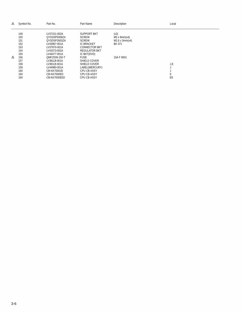
3-6
149 LV37151-002A SUPPORT BKT (x2)150 QYSSSP5008ZA SCREW M5 x 8mm(x4)151 QYSDSP2603ZA SCREW M2.6 x 3mm(x4)152 LV43967-001A IC BRACKET BK 371153 LV37970-001A CONNECTOR BKT154 LV43373-002A REGULATOR BKT155 LV44477-001A IC BKT(DVD)
156 QMFZ039-150-T FUSE 15A F 9001157 LV38118-001A SHIELD COVER158 LV38118-001A SHIELD COVER J,E159 LV44980-001A LABEL(MERCURY) J160 CB-NX7000JD CPU CB ASSY J160 CB-NX7000ED CPU CB ASSY E160 CB-NX7000EED CPU CB ASSY EE
Symbol No. Part No. Part Name Description Local

3-7
<MEMO>
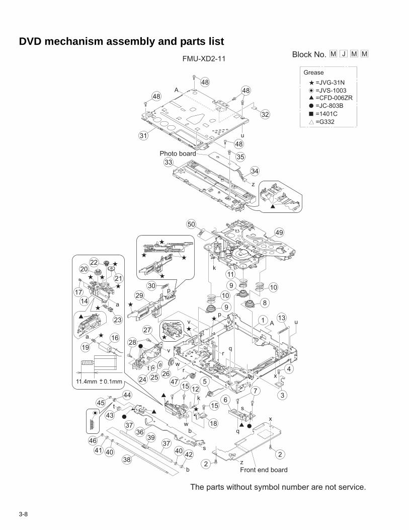
3-8
DVD mechanism assembly and parts list
Grease
=1401C
=G332
=JVS-1003
=JVG-31N
=CFD-006ZR
=JC-803B
11.4mm 0.1mm
k
w
w
v
v
Block No. M MMJFMU-XD2-11
a
a
b
b
k
p
p
q
x
qr
r
s
s
t
t
A
A
u
u
x
CN2
z
Photo board
Front end board
z
34
48
32
35
48
49
31
48
48
33
20
17
14
30
29
24 2547 5
13
3
4
1
10
810
9
11
9
12
15
7
18
4240
3739
37
46
45
43
44
41 4038
36
2
2
6
26
27
19
23
28
15
16
22
21
The parts without symbol number are not service.
50

3-9
DVD mechanismBlock No. [M][J][M][M]
Symbol No. Part No. Part Name Description Local
1 LV11434-004A FRAME UNIT 2 VKZ4539-054 MINI SCREW (x2) 3 LV45021-001A STOPPER 4 LV44959-002A SPECIAL SCREW 5 LV44907-004A L.A.SPRING R 6 LV37639-002A L ARM HOLDER 7 VKZ4539-054 MINI SCREW (x2) 8 LV37640-001A DAMPER(R) 9 LV37641-001A DAMPER(F) (x2) 10 LV45074-001A DAMPER SPRING B (x2) 11 LV45073-001A DAMPER SPRING A 12 LV44897-002A FLOATING SPRING 13 LV44894-001A LOCK SLIDER SP. 14 LV11436-001A MOTOR HOLDER 15 LV45135-001A MINI TAP SCREW (x3) 16 QAR0465-001 LOAD MOTOR 17 QYSPSPU1425MA SCREW M1.4 x 2.5mm(x2) 18 LV37642-001A MOTOR TH SPRING 19 LV37643-001A MOTOR WORM GEAR 20 LV37644-002A M WHEEL GEAR 21 LV37645-002A M CONNECT GEAR 22 LV37646-001A A WORM GEAR 23 LV37647-001A A WHEEL GEAR 24 LV37648-001A ACT GEAR 25 LV37649-001A A CONNECT GEAR 26 LV37650-001A LOADING GEAR 27 LV22553-003A GEAR BASE 28 VKZ4539-054 MINI SCREW (x2) 29 LV37688-002A SLIDE CAM ASSY 30 LV45090-001A S.CAM SPRING 31 LV11437-003A TOP COVER 32 LV45157-001A SPACER 33 LV11438-003A DISC PLATE 34 WJM0493-001A-E E-SI C WIRE C-F 35 LV44586-001A SPECIAL SCREW 36 LV22555-002A L ARM ASSY 37 LV44902-001A ROLLER (x2) 38 LV44903-001A ROLLER SHAFT 39 LV37652-002A SHAFT GUIDE 40 LV44960-001A SLIT WASHER (x2) 41 LV44904-001A R COLLAR L 42 LV44905-001A R COLLAR R 43 LV37653-001A R CONNECT GEAR 44 LV37654-001A R MIDDLE GEAR 45 QYWDL1735250 SLIT WASHER 3.5mm/1.7mm x 0.25mm 46 LV37655-001A ROLLER GEAR 47 LV44906-005A L.A.SPRING L 48 VKZ4539-054 MINI SCREW (x5) 49 CM-FMUXD1D TRA MECHA UNIT 50 LV44910-002A CLAMPER SPRING

3-10
Electrical parts listMain board
Block No. [0][1] Symbol No. Part No. Part Name Description Local
IC111 TEF6601T/V2-X IC J IC111 TEF6606T/V2-X IC E,EE
IC121 LC72725KM-X IC E,EEIC151 TEF6601T/V2-X IC J,EIC161 LC72725KM-X IC J,EIC201 NJM2505F-X ICIC211 NJM2505F-X ICIC251 MM1228XF-X ICIC261 NJM2535V-X ICIC301 TDA7416 ICIC331 NJM4565M-WE ICIC332 NJM4565M-WE ICIC333 NJM4565M-WE IC
IC371 TB2926AHQ IC IC701 UPD78F1178GF7B IC(PROGRAMED)
IC731 S-80824CNNB-G-W ICIC741 BR24L32F-W-X IC(DIGITAL)
IC911 R2S25400DS-E ICIC912 BH33MA3WHFV-W IC
IC921 BA9743AFV-X ICIC922 TC7SH08FU-X ICIC931 NJM2396F09 ICIC951 TC7WT241FU-X ICIC952 TC7WT241FU-X ICIC961 BA6956AN IC
Q1401 3SK195-W TRANSISTOR J,EQ3031 2SC3928A/QR/-X TRANSISTORQ3031 or 2SD601A/QR/-X TRANSISTORQ3031 or 2SC2412K/R/-X TRANSISTORQ3032 ISA1530AC1/QR/X TRANSISTORQ3071 RT1N441C-X TRANSISTORQ3072 RT1P441C-X DIGI TRANSISTORQ3073 RT1N441C-X TRANSISTORQ3074 2SC3928A/QR/-X TRANSISTORQ3074 or 2SD601A/QR/-X TRANSISTORQ3074 or 2SC2412K/R/-X TRANSISTORQ3151 2SD2114K/VW/-X TRANSISTORQ3251 2SD2114K/VW/-X TRANSISTORQ3351 2SD2114K/VW/-X TRANSISTORQ3451 2SD2114K/VW/-X TRANSISTORQ3551 2SD2114K/VW/-X TRANSISTORQ7001 RT1P441C-X DIGI TRANSISTORQ9131 RSQ025P03-W TRANSISTORQ9132 RT1N141C-X DIGI TRANSISTORQ9132 or UN2211-X TRANSISTORQ9132 or DTC114EKA-X DIGI TRANSISTORQ9151 RT1P441C-X DIGI TRANSISTORQ9152 RT1N441C-X TRANSISTORQ9241 ISA1530AC1/QR/X TRANSISTORQ9242 2SC3928A/QR/-X TRANSISTORQ9242 or 2SD601A/QR/-X TRANSISTORQ9242 or 2SC2412K/R/-X TRANSISTORQ9243 RTQ035N03-W MOS FETQ9251 ISA1530AC1/QR/X TRANSISTORQ9401 RT1P141C-X DIGI TRANSISTORQ9401 or UN2111-X TRANSISTORQ9401 or DTA114EKA-X DIGI TRANSISTORQ9402 RT1P141C-X DIGI TRANSISTORQ9402 or UN2111-X TRANSISTORQ9402 or DTA114EKA-X DIGI TRANSISTORQ9403 RT1P141C-X DIGI TRANSISTORQ9403 or UN2111-X TRANSISTORQ9403 or DTA114EKA-X DIGI TRANSISTORQ9451 RT1N141C-X DIGI TRANSISTORQ9451 or UN2211-X TRANSISTORQ9451 or DTC114EKA-X DIGI TRANSISTORQ9453 2SC3928A/QR/-X TRANSISTORQ9453 or 2SD601A/QR/-X TRANSISTORQ9453 or 2SC2412K/R/-X TRANSISTORQ9454 RT1N141C-X DIGI TRANSISTORQ9454 or UN2211-X TRANSISTOR
Q9454 or DTC114EKA-X DIGI TRANSISTORQ9461 RT1N441C-X TRANSISTORQ9462 ISA1530AC1/QR/X TRANSISTORQ9551 RT1N141C-X DIGI TRANSISTORQ9551 or UN2211-X TRANSISTORQ9551 or DTC114EKA-X DIGI TRANSISTORQ9561 RT1P441C-X DIGI TRANSISTORQ9562 RT1N441C-X TRANSISTORQ9601 RT1N141C-X DIGI TRANSISTORQ9601 or UN2211-X TRANSISTORQ9601 or DTC114EKA-X DIGI TRANSISTORQ9701 RT1N141C-X DIGI TRANSISTORQ9701 or UN2211-X TRANSISTORQ9701 or DTC114EKA-X DIGI TRANSISTORQ9751 ISA1530AC1/QR/X TRANSISTOR E,EE
D1001 MA111-X SI DIODE J,ED1002 MA111-X SI DIODE J,ED2001 MA111-X SI DIODED2002 MA111-X SI DIODED2101 MA111-X SI DIODED2102 MA111-X SI DIODED2501 MA111-X SI DIODED2502 MA111-X SI DIODED3071 MA8110/M/-X Z DIODED3151 MC2836-X DIODED3251 MC2836-X DIODED3551 MA111-X SI DIODED7351 MA111-X SI DIODE
D9001 1N5401-F64 SI DIODED9003 MA22D23-X SB DIODED9004 MA22D23-X SB DIODE JD9005 MA22D23-X SB DIODE JD9006 MA22D23-X SB DIODED9051 MA22D23-X SB DIODED9151 MA111-X SI DIODED9241 RB051L-40-X SB DIODED9251 MA22D23-X SB DIODED9252 MA22D23-X SB DIODED9253 MA8120/M/-X Z DIODED9254 MA111-X SI DIODED9301 MA8033/H/-X Z DIODED9401 MA8110/M/-X Z DIODED9402 MC2836-X DIODED9403 MA111-X SI DIODED9451 MC2836-X DIODED9452 MA111-X SI DIODED9601 MA22D23-X SB DIODED9602 MA8056/M/-X Z DIODED9701 MA8047/M/-X Z DIODED9702 MA111-X SI DIODED9703 MA111-X SI DIODED9751 MA111-X SI DIODE E,EE
C1001 NDC31HJ-150X C CAPACITOR 15pF 50V JC1002 NDC31HJ-220X C CAPACITOR 22pF 50V JC1003 NCB31HK-102X C CAPACITOR 1000pF 50V KC1004 NDC31HJ-7R0X C CAPACITOR 7pF 50V JC1005 NDC31HJ-6R0X C CAPACITOR 6pF 50V JC1006 NDC31HJ-2R0X C CAPACITOR 2pF 50V JC1007 NCB31HK-104X C CAPACITOR 0.1uF 50V KC1101 NCB31CK-224X C CAPACITOR 0.22uF 16V KC1102 NCJ21CK-106X-R C CAPACITOR 10uF 16V KC1103 NCB31CK-224X C CAPACITOR 0.22uF 16V KC1104 NCB31CK-105X C CAPACITOR 1uF 16V KC1105 NCB31CK-105X C CAPACITOR 1uF 16V KC1106 NCB31CK-224X C CAPACITOR 0.22uF 16V KC1107 NCB31HK-104X C CAPACITOR 0.1uF 50V KC1108 NDC31HJ-180X C CAPACITOR 18pF 50V JC1109 NCB31CK-105X C CAPACITOR 1uF 16V KC1110 NCB31HK-103X C CAPACITOR 0.01uF 50V KC1111 NCB31HK-103X C CAPACITOR 0.01uF 50V KC1112 NCB31HK-104X C CAPACITOR 0.1uF 50V KC1113 NCB31HK-103X C CAPACITOR 0.01uF 50V KC1114 NCB31HK-103X C CAPACITOR 0.01uF 50V KC1115 NCB31HK-104X C CAPACITOR 0.1uF 50V K
Symbol No. Part No. Part Name Description Local
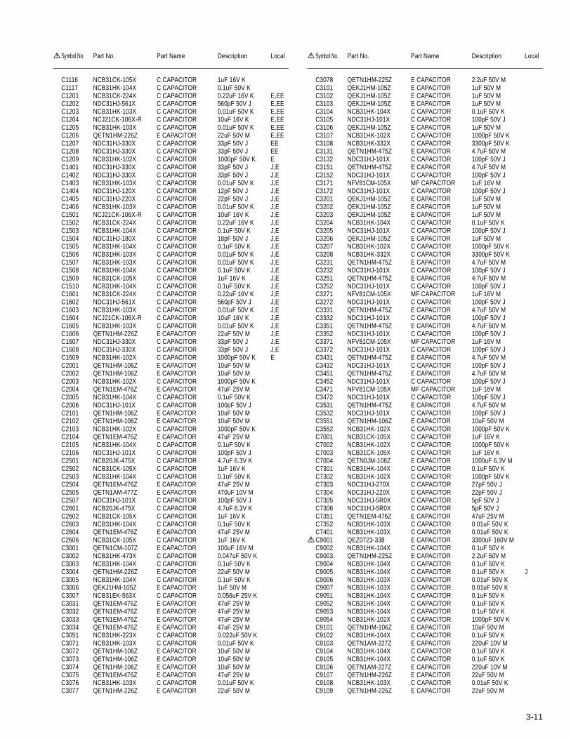
3-11
C1116 NCB31CK-105X C CAPACITOR 1uF 16V KC1117 NCB31HK-104X C CAPACITOR 0.1uF 50V KC1201 NCB31CK-224X C CAPACITOR 0.22uF 16V K E,EEC1202 NDC31HJ-561X C CAPACITOR 560pF 50V J E,EEC1203 NCB31HK-103X C CAPACITOR 0.01uF 50V K E,EEC1204 NCJ21CK-106X-R C CAPACITOR 10uF 16V K E,EEC1205 NCB31HK-103X C CAPACITOR 0.01uF 50V K E,EEC1206 QETN1HM-226Z E CAPACITOR 22uF 50V M E,EEC1207 NDC31HJ-330X C CAPACITOR 33pF 50V J EEC1208 NDC31HJ-330X C CAPACITOR 33pF 50V J EEC1209 NCB31HK-102X C CAPACITOR 1000pF 50V K EC1401 NDC31HJ-330X C CAPACITOR 33pF 50V J J,EC1402 NDC31HJ-330X C CAPACITOR 33pF 50V J J,EC1403 NCB31HK-103X C CAPACITOR 0.01uF 50V K J,EC1404 NDC31HJ-120X C CAPACITOR 12pF 50V J J,EC1405 NDC31HJ-220X C CAPACITOR 22pF 50V J J,EC1406 NCB31HK-103X C CAPACITOR 0.01uF 50V K J,EC1501 NCJ21CK-106X-R C CAPACITOR 10uF 16V K J,EC1502 NCB31CK-224X C CAPACITOR 0.22uF 16V K J,EC1503 NCB31HK-104X C CAPACITOR 0.1uF 50V K J,EC1504 NDC31HJ-180X C CAPACITOR 18pF 50V J J,EC1505 NCB31HK-104X C CAPACITOR 0.1uF 50V K J,EC1506 NCB31HK-103X C CAPACITOR 0.01uF 50V K J,EC1507 NCB31HK-103X C CAPACITOR 0.01uF 50V K J,EC1508 NCB31HK-104X C CAPACITOR 0.1uF 50V K J,EC1509 NCB31CK-105X C CAPACITOR 1uF 16V K J,EC1510 NCB31HK-104X C CAPACITOR 0.1uF 50V K J,EC1601 NCB31CK-224X C CAPACITOR 0.22uF 16V K J,EC1602 NDC31HJ-561X C CAPACITOR 560pF 50V J J,EC1603 NCB31HK-103X C CAPACITOR 0.01uF 50V K J,EC1604 NCJ21CK-106X-R C CAPACITOR 10uF 16V K J,EC1605 NCB31HK-103X C CAPACITOR 0.01uF 50V K J,EC1606 QETN1HM-226Z E CAPACITOR 22uF 50V M J,EC1607 NDC31HJ-330X C CAPACITOR 33pF 50V J J,EC1608 NDC31HJ-330X C CAPACITOR 33pF 50V J J,EC1609 NCB31HK-102X C CAPACITOR 1000pF 50V K EC2001 QETN1HM-106Z E CAPACITOR 10uF 50V MC2002 QETN1HM-106Z E CAPACITOR 10uF 50V MC2003 NCB31HK-102X C CAPACITOR 1000pF 50V KC2004 QETN1EM-476Z E CAPACITOR 47uF 25V MC2005 NCB31HK-104X C CAPACITOR 0.1uF 50V KC2006 NDC31HJ-101X C CAPACITOR 100pF 50V JC2101 QETN1HM-106Z E CAPACITOR 10uF 50V MC2102 QETN1HM-106Z E CAPACITOR 10uF 50V MC2103 NCB31HK-102X C CAPACITOR 1000pF 50V KC2104 QETN1EM-476Z E CAPACITOR 47uF 25V MC2105 NCB31HK-104X C CAPACITOR 0.1uF 50V KC2106 NDC31HJ-101X C CAPACITOR 100pF 50V JC2501 NCB20JK-475X C CAPACITOR 4.7uF 6.3V KC2502 NCB31CK-105X C CAPACITOR 1uF 16V KC2503 NCB31HK-104X C CAPACITOR 0.1uF 50V KC2504 QETN1EM-476Z E CAPACITOR 47uF 25V MC2505 QETN1AM-477Z E CAPACITOR 470uF 10V MC2507 NDC31HJ-101X C CAPACITOR 100pF 50V JC2601 NCB20JK-475X C CAPACITOR 4.7uF 6.3V KC2602 NCB31CK-105X C CAPACITOR 1uF 16V KC2603 NCB31HK-104X C CAPACITOR 0.1uF 50V KC2604 QETN1EM-476Z E CAPACITOR 47uF 25V MC2606 NCB31CK-105X C CAPACITOR 1uF 16V KC3001 QETN1CM-107Z E CAPACITOR 100uF 16V MC3002 NCB31HK-473X C CAPACITOR 0.047uF 50V KC3003 NCB31HK-104X C CAPACITOR 0.1uF 50V KC3004 QETN1HM-226Z E CAPACITOR 22uF 50V MC3005 NCB31HK-104X C CAPACITOR 0.1uF 50V KC3006 QEKJ1HM-105Z E CAPACITOR 1uF 50V MC3007 NCB31EK-563X C CAPACITOR 0.056uF 25V KC3031 QETN1EM-476Z E CAPACITOR 47uF 25V MC3032 QETN1EM-476Z E CAPACITOR 47uF 25V MC3033 QETN1EM-476Z E CAPACITOR 47uF 25V MC3034 QETN1EM-476Z E CAPACITOR 47uF 25V MC3051 NCB31HK-223X C CAPACITOR 0.022uF 50V KC3071 NCB31HK-103X C CAPACITOR 0.01uF 50V KC3072 QETN1HM-106Z E CAPACITOR 10uF 50V MC3073 QETN1HM-106Z E CAPACITOR 10uF 50V MC3074 QETN1HM-106Z E CAPACITOR 10uF 50V MC3075 QETN1EM-476Z E CAPACITOR 47uF 25V MC3076 NCB31HK-103X C CAPACITOR 0.01uF 50V KC3077 QETN1HM-226Z E CAPACITOR 22uF 50V M
Symbol No. Part No. Part Name Description Local
C3078 QETN1HM-225Z E CAPACITOR 2.2uF 50V MC3101 QEKJ1HM-105Z E CAPACITOR 1uF 50V MC3102 QEKJ1HM-105Z E CAPACITOR 1uF 50V MC3103 QEKJ1HM-105Z E CAPACITOR 1uF 50V MC3104 NCB31HK-104X C CAPACITOR 0.1uF 50V KC3105 NDC31HJ-101X C CAPACITOR 100pF 50V JC3106 QEKJ1HM-105Z E CAPACITOR 1uF 50V MC3107 NCB31HK-102X C CAPACITOR 1000pF 50V KC3108 NCB31HK-332X C CAPACITOR 3300pF 50V KC3131 QETN1HM-475Z E CAPACITOR 4.7uF 50V MC3132 NDC31HJ-101X C CAPACITOR 100pF 50V JC3151 QETN1HM-475Z E CAPACITOR 4.7uF 50V MC3152 NDC31HJ-101X C CAPACITOR 100pF 50V JC3171 NFV81CM-105X MF CAPACITOR 1uF 16V MC3172 NDC31HJ-101X C CAPACITOR 100pF 50V JC3201 QEKJ1HM-105Z E CAPACITOR 1uF 50V MC3202 QEKJ1HM-105Z E CAPACITOR 1uF 50V MC3203 QEKJ1HM-105Z E CAPACITOR 1uF 50V MC3204 NCB31HK-104X C CAPACITOR 0.1uF 50V KC3205 NDC31HJ-101X C CAPACITOR 100pF 50V JC3206 QEKJ1HM-105Z E CAPACITOR 1uF 50V MC3207 NCB31HK-102X C CAPACITOR 1000pF 50V KC3208 NCB31HK-332X C CAPACITOR 3300pF 50V KC3231 QETN1HM-475Z E CAPACITOR 4.7uF 50V MC3232 NDC31HJ-101X C CAPACITOR 100pF 50V JC3251 QETN1HM-475Z E CAPACITOR 4.7uF 50V MC3252 NDC31HJ-101X C CAPACITOR 100pF 50V JC3271 NFV81CM-105X MF CAPACITOR 1uF 16V MC3272 NDC31HJ-101X C CAPACITOR 100pF 50V JC3331 QETN1HM-475Z E CAPACITOR 4.7uF 50V MC3332 NDC31HJ-101X C CAPACITOR 100pF 50V JC3351 QETN1HM-475Z E CAPACITOR 4.7uF 50V MC3352 NDC31HJ-101X C CAPACITOR 100pF 50V JC3371 NFV81CM-105X MF CAPACITOR 1uF 16V MC3372 NDC31HJ-101X C CAPACITOR 100pF 50V JC3431 QETN1HM-475Z E CAPACITOR 4.7uF 50V MC3432 NDC31HJ-101X C CAPACITOR 100pF 50V JC3451 QETN1HM-475Z E CAPACITOR 4.7uF 50V MC3452 NDC31HJ-101X C CAPACITOR 100pF 50V JC3471 NFV81CM-105X MF CAPACITOR 1uF 16V MC3472 NDC31HJ-101X C CAPACITOR 100pF 50V JC3531 QETN1HM-475Z E CAPACITOR 4.7uF 50V MC3532 NDC31HJ-101X C CAPACITOR 100pF 50V JC3551 QETN1HM-106Z E CAPACITOR 10uF 50V MC3552 NCB31HK-102X C CAPACITOR 1000pF 50V KC7001 NCB31CK-105X C CAPACITOR 1uF 16V KC7002 NCB31HK-102X C CAPACITOR 1000pF 50V KC7003 NCB31CK-105X C CAPACITOR 1uF 16V KC7004 QETN0JM-108Z E CAPACITOR 1000uF 6.3V MC7301 NCB31HK-104X C CAPACITOR 0.1uF 50V KC7302 NCB31HK-102X C CAPACITOR 1000pF 50V KC7303 NDC31HJ-270X C CAPACITOR 27pF 50V JC7304 NDC31HJ-220X C CAPACITOR 22pF 50V JC7305 NDC31HJ-5R0X C CAPACITOR 5pF 50V JC7306 NDC31HJ-5R0X C CAPACITOR 5pF 50V JC7351 QETN1EM-476Z E CAPACITOR 47uF 25V MC7352 NCB31HK-103X C CAPACITOR 0.01uF 50V KC7401 NCB31HK-103X C CAPACITOR 0.01uF 50V K
C9001 QEZ0723-338 E CAPACITOR 3300uF 160V MC9002 NCB31HK-104X C CAPACITOR 0.1uF 50V KC9003 QETN1HM-225Z E CAPACITOR 2.2uF 50V MC9004 NCB31HK-104X C CAPACITOR 0.1uF 50V KC9005 NCB31HK-104X C CAPACITOR 0.1uF 50V K JC9006 NCB31HK-103X C CAPACITOR 0.01uF 50V KC9007 NCB31HK-103X C CAPACITOR 0.01uF 50V KC9051 NCB31HK-104X C CAPACITOR 0.1uF 50V KC9052 NCB31HK-104X C CAPACITOR 0.1uF 50V KC9053 NCB31HK-104X C CAPACITOR 0.1uF 50V KC9054 NCB31HK-102X C CAPACITOR 1000pF 50V KC9101 QETN1HM-106Z E CAPACITOR 10uF 50V MC9102 NCB31HK-104X C CAPACITOR 0.1uF 50V KC9103 QETN1AM-227Z E CAPACITOR 220uF 10V MC9104 NCB31HK-104X C CAPACITOR 0.1uF 50V KC9105 NCB31HK-104X C CAPACITOR 0.1uF 50V KC9106 QETN1AM-227Z E CAPACITOR 220uF 10V MC9107 QETN1HM-226Z E CAPACITOR 22uF 50V MC9108 NCB31HK-103X C CAPACITOR 0.01uF 50V KC9109 QETN1HM-226Z E CAPACITOR 22uF 50V M
Symbol No. Part No. Part Name Description Local

3-12
C9151 QETN0JM-108Z E CAPACITOR 1000uF 6.3V MC9152 NCB31HK-103X C CAPACITOR 0.01uF 50V KC9153 NCB31CK-105X C CAPACITOR 1uF 16V KC9201 NCB31HK-103X C CAPACITOR 0.01uF 50V KC9202 NCB31HK-104X C CAPACITOR 0.1uF 50V KC9203 NCB31HK-272X C CAPACITOR 2700pF 50V KC9205 NCB31HK-104X C CAPACITOR 0.1uF 50V KC9211 NCB31CK-105X C CAPACITOR 1uF 16V KC9212 NCB31HK-222X C CAPACITOR 2200pF 50V KC9214 NCB31HK-682X C CAPACITOR 6800pF 50V KC9215 NCB31HK-104X C CAPACITOR 0.1uF 50V KC9241 NCJ11EK-106X-R C CAPACITOR 10uF 25VC9242 NDC31HJ-221X C CAPACITOR 220pF 50V JC9243 NCJ11EK-106X-R C CAPACITOR 10uF 25VC9244 QETN1EM-476Z E CAPACITOR 47uF 25V MC9251 NCB31HK-104X C CAPACITOR 0.1uF 50V KC9252 NCF21HZ-105X C CAPACITOR 1uF 50V ZC9253 NCB31HK-104X C CAPACITOR 0.1uF 50V KC9254 NCB31CK-105X C CAPACITOR 1uF 16V KC9255 QETN1EM-476Z E CAPACITOR 47uF 25V MC9301 QEKJ1EM-106Z E CAPACITOR 10uF 25V MC9302 NCB31HK-104X C CAPACITOR 0.1uF 50V KC9303 QEKJ1EM-106Z E CAPACITOR 10uF 25V MC9304 NCB31HK-103X C CAPACITOR 0.01uF 50V KC9401 QETN1EM-476Z E CAPACITOR 47uF 25V MC9402 QETN1EM-476Z E CAPACITOR 47uF 25V MC9451 NCB31HK-104X C CAPACITOR 0.1uF 50V KC9453 QETN1HM-226Z E CAPACITOR 22uF 50V MC9454 NCB31CK-105X C CAPACITOR 1uF 16V KC9501 NCB31HK-103X C CAPACITOR 0.01uF 50V KC9502 NCB31HK-103X C CAPACITOR 0.01uF 50V KC9551 NCB31HK-104X C CAPACITOR 0.1uF 50V KC9601 QETN1CM-107Z E CAPACITOR 100uF 16V MC9602 NCB31HK-473X C CAPACITOR 0.047uF 50V KC9701 QETN1HM-106Z E CAPACITOR 10uF 50V MC9702 NCB31HK-473X C CAPACITOR 0.047uF 50V KC9703 NCB31HK-102X C CAPACITOR 1000pF 50V KC9751 QETN1HM-106Z E CAPACITOR 10uF 50V M E,EEC9752 NCB31HK-103X C CAPACITOR 0.01uF 50V K E,EEC9753 NDC31HJ-220X C CAPACITOR 22pF 50V J E,EEC9802 NCB31HK-102X C CAPACITOR 1000pF 50V K
R1001 NRSA63J-474X MG RESISTOR 470kΩ 1/16W JR1002 NRSA63J-474X MG RESISTOR 470kΩ 1/16W JR1101 NRSA63J-472X MG RESISTOR 4.7kΩ 1/16W JR1102 NRS181J-220X MG RESISTOR 22Ω 1/8W JR1105 NRSA63J-472X MG RESISTOR 4.7kΩ 1/16W JR1106 NRSA63J-472X MG RESISTOR 4.7kΩ 1/16W JR1111 NRSA63J-153X MG RESISTOR 15kΩ 1/16W J JR1111 NRSA63J-0R0X MG RESISTOR 0Ω 1/16W J E,EER1112 NRSA63J-153X MG RESISTOR 15kΩ 1/16W J JR1112 NRSA63J-0R0X MG RESISTOR 0Ω 1/16W J E,EER1113 NRSA63J-473X MG RESISTOR 47kΩ 1/16W JR1114 NRSA63J-473X MG RESISTOR 47kΩ 1/16W JR1201 NRSA63J-222X MG RESISTOR 2.2kΩ 1/16W J E,EER1202 NRSA63J-0R0X MG RESISTOR 0Ω 1/16W J EER1203 NRSA63J-222X MG RESISTOR 2.2kΩ 1/16W J E,EER1401 NRSA63J-104X MG RESISTOR 100kΩ 1/16W J J,ER1402 NRSA63J-394X MG RESISTOR 390kΩ 1/16W J J,ER1403 NRSA63J-104X MG RESISTOR 100kΩ 1/16W J J,ER1404 NRSA63J-823X MG RESISTOR 82kΩ 1/16W J J,ER1405 NRSA63J-0R0X MG RESISTOR 0Ω 1/16W J J,ER1406 NRSA63J-0R0X MG RESISTOR 0Ω 1/16W J J,ER1502 NRSA63J-472X MG RESISTOR 4.7kΩ 1/16W J J,ER1503 NRS181J-220X MG RESISTOR 22Ω 1/8W J J,ER1506 NRSA63J-472X MG RESISTOR 4.7kΩ 1/16W J J,ER1507 NRSA63J-472X MG RESISTOR 4.7kΩ 1/16W J J,ER1551 NRS181J-4R7X MG RESISTOR 4.7Ω 1/8W JR1552 NRSA63J-0R0X MG RESISTOR 0Ω 1/16W JR1553 NRSA63J-0R0X MG RESISTOR 0Ω 1/16W J J,ER1554 NRS181J-4R7X MG RESISTOR 4.7Ω 1/8W J J,ER1601 NRSA63J-222X MG RESISTOR 2.2kΩ 1/16W J J,ER1602 NRSA63J-0R0X MG RESISTOR 0Ω 1/16W J J,ER1603 NRSA63J-222X MG RESISTOR 2.2kΩ 1/16W J J,ER2001 NRSA63J-471X MG RESISTOR 470Ω 1/16W JR2002 NRSA63J-471X MG RESISTOR 470Ω 1/16W JR2003 NRSA63J-104X MG RESISTOR 100kΩ 1/16W JR2004 NRSA63J-104X MG RESISTOR 100kΩ 1/16W J
Symbol No. Part No. Part Name Description Local
R2005 NRSA63J-390X MG RESISTOR 39Ω 1/16W JR2006 NRSA63J-100X MG RESISTOR 10Ω 1/16W JR2007 NRSA63J-0R0X MG RESISTOR 0Ω 1/16W JR2008 NRSA63J-0R0X MG RESISTOR 0Ω 1/16W JR2101 NRSA63J-471X MG RESISTOR 470Ω 1/16W JR2102 NRSA63J-471X MG RESISTOR 470Ω 1/16W JR2103 NRSA63J-104X MG RESISTOR 100kΩ 1/16W JR2104 NRSA63J-104X MG RESISTOR 100kΩ 1/16W JR2105 NRSA63J-390X MG RESISTOR 39Ω 1/16W JR2106 NRSA63J-100X MG RESISTOR 10Ω 1/16W JR2107 NRSA63J-0R0X MG RESISTOR 0Ω 1/16W JR2108 NRSA63J-0R0X MG RESISTOR 0Ω 1/16W JR2501 NRSA63J-100X MG RESISTOR 10Ω 1/16W JR2502 NRSA63J-750X MG RESISTOR 75Ω 1/16W JR2503 NRSA63J-103X MG RESISTOR 10kΩ 1/16W JR2504 NRSA63J-105X MG RESISTOR 1MΩ 1/16W JR2505 NRSA63J-0R0X MG RESISTOR 0Ω 1/16W JR2601 NRSA63J-100X MG RESISTOR 10Ω 1/16W JR2602 NRSA63J-0R0X MG RESISTOR 0Ω 1/16W JR2603 NRSA63J-181X MG RESISTOR 180Ω 1/16W JR2604 NRSA63J-332X MG RESISTOR 3.3kΩ 1/16W JR3001 NRSA63J-471X MG RESISTOR 470Ω 1/16W JR3003 NRSA63J-101X MG RESISTOR 100Ω 1/16W JR3004 NRSA63J-0R0X MG RESISTOR 0Ω 1/16W JR3005 NRSA63J-222X MG RESISTOR 2.2kΩ 1/16W JR3031 NRSA63J-332X MG RESISTOR 3.3kΩ 1/16W JR3033 NRSA63J-222X MG RESISTOR 2.2kΩ 1/16W JR3034 NRSA63J-472X MG RESISTOR 4.7kΩ 1/16W JR3055 NRSA63J-0R0X MG RESISTOR 0Ω 1/16W JR3056 NRSA63J-0R0X MG RESISTOR 0Ω 1/16W JR3071 NRSA63J-222X MG RESISTOR 2.2kΩ 1/16W JR3072 NRSA63J-100X MG RESISTOR 10Ω 1/16W JR3073 NRSA63J-273X MG RESISTOR 27kΩ 1/16W JR3074 NRSA63J-473X MG RESISTOR 47kΩ 1/16W JR3075 NRSA63J-473X MG RESISTOR 47kΩ 1/16W JR3076 NRSA63J-103X MG RESISTOR 10kΩ 1/16W JR3101 NRSA63J-473X MG RESISTOR 47kΩ 1/16W JR3102 NRSA63J-222X MG RESISTOR 2.2kΩ 1/16W JR3103 NRSA63J-473X MG RESISTOR 47kΩ 1/16W JR3104 NRSA63J-0R0X MG RESISTOR 0Ω 1/16W JR3105 NRSA63J-151X MG RESISTOR 150Ω 1/16W JR3106 NRSA63J-471X MG RESISTOR 470Ω 1/16W JR3131 NRSA63J-102X MG RESISTOR 1kΩ 1/16W JR3132 NRSA63J-473X MG RESISTOR 47kΩ 1/16W JR3133 NRSA63J-183X MG RESISTOR 18kΩ 1/16W JR3134 NRSA63J-123X MG RESISTOR 12kΩ 1/16W JR3151 NRSA63J-102X MG RESISTOR 1kΩ 1/16W JR3152 NRSA63J-473X MG RESISTOR 47kΩ 1/16W JR3153 NRSA63J-201X MG RESISTOR 200Ω 1/16W JR3154 NRSA63J-201X MG RESISTOR 200Ω 1/16W JR3155 NRSA63J-222X MG RESISTOR 2.2kΩ 1/16W JR3171 NRSA63J-101X MG RESISTOR 100Ω 1/16W JR3172 NRSA63J-102X MG RESISTOR 1kΩ 1/16W JR3201 NRSA63J-473X MG RESISTOR 47kΩ 1/16W JR3202 NRSA63J-222X MG RESISTOR 2.2kΩ 1/16W JR3203 NRSA63J-473X MG RESISTOR 47kΩ 1/16W JR3204 NRSA63J-0R0X MG RESISTOR 0Ω 1/16W JR3205 NRSA63J-151X MG RESISTOR 150Ω 1/16W JR3206 NRSA63J-471X MG RESISTOR 470Ω 1/16W JR3231 NRSA63J-102X MG RESISTOR 1kΩ 1/16W JR3232 NRSA63J-473X MG RESISTOR 47kΩ 1/16W JR3233 NRSA63J-183X MG RESISTOR 18kΩ 1/16W JR3234 NRSA63J-123X MG RESISTOR 12kΩ 1/16W JR3251 NRSA63J-102X MG RESISTOR 1kΩ 1/16W JR3252 NRSA63J-473X MG RESISTOR 47kΩ 1/16W JR3253 NRSA63J-201X MG RESISTOR 200Ω 1/16W JR3254 NRSA63J-201X MG RESISTOR 200Ω 1/16W JR3255 NRSA63J-222X MG RESISTOR 2.2kΩ 1/16W JR3271 NRSA63J-101X MG RESISTOR 100Ω 1/16W JR3272 NRSA63J-102X MG RESISTOR 1kΩ 1/16W JR3331 NRSA63J-102X MG RESISTOR 1kΩ 1/16W JR3332 NRSA63J-473X MG RESISTOR 47kΩ 1/16W JR3333 NRSA63J-183X MG RESISTOR 18kΩ 1/16W JR3334 NRSA63J-123X MG RESISTOR 12kΩ 1/16W JR3351 NRSA63J-102X MG RESISTOR 1kΩ 1/16W JR3352 NRSA63J-473X MG RESISTOR 47kΩ 1/16W JR3353 NRSA63J-201X MG RESISTOR 200Ω 1/16W JR3354 NRSA63J-201X MG RESISTOR 200Ω 1/16W J
Symbol No. Part No. Part Name Description Local

3-13
R3355 NRSA63J-222X MG RESISTOR 2.2kΩ 1/16W JR3371 NRSA63J-101X MG RESISTOR 100Ω 1/16W JR3372 NRSA63J-102X MG RESISTOR 1kΩ 1/16W JR3431 NRSA63J-102X MG RESISTOR 1kΩ 1/16W JR3432 NRSA63J-473X MG RESISTOR 47kΩ 1/16W JR3433 NRSA63J-183X MG RESISTOR 18kΩ 1/16W JR3434 NRSA63J-123X MG RESISTOR 12kΩ 1/16W JR3451 NRSA63J-102X MG RESISTOR 1kΩ 1/16W JR3452 NRSA63J-473X MG RESISTOR 47kΩ 1/16W JR3453 NRSA63J-201X MG RESISTOR 200Ω 1/16W JR3454 NRSA63J-201X MG RESISTOR 200Ω 1/16W JR3455 NRSA63J-222X MG RESISTOR 2.2kΩ 1/16W JR3471 NRSA63J-101X MG RESISTOR 100Ω 1/16W JR3472 NRSA63J-102X MG RESISTOR 1kΩ 1/16W JR3531 NRSA63J-102X MG RESISTOR 1kΩ 1/16W JR3532 NRSA63J-473X MG RESISTOR 47kΩ 1/16W JR3533 NRSA63J-183X MG RESISTOR 18kΩ 1/16W JR3534 NRSA63J-123X MG RESISTOR 12kΩ 1/16W JR3551 NRSA63J-102X MG RESISTOR 1kΩ 1/16W JR3552 NRSA63J-103X MG RESISTOR 10kΩ 1/16W JR3553 NRSA63J-201X MG RESISTOR 200Ω 1/16W JR3554 NRSA63J-201X MG RESISTOR 200Ω 1/16W JR3555 NRSA63J-222X MG RESISTOR 2.2kΩ 1/16W JR7001 NRSA63J-102X MG RESISTOR 1kΩ 1/16W JR7002 NRSA63J-102X MG RESISTOR 1kΩ 1/16W JR7004 NRSA63J-102X MG RESISTOR 1kΩ 1/16W JR7009 NRSA63J-222X MG RESISTOR 2.2kΩ 1/16W JR7010 NRSA63J-0R0X MG RESISTOR 0Ω 1/16W JR7011 NRSA63J-102X MG RESISTOR 1kΩ 1/16W JR7012 NRSA63J-102X MG RESISTOR 1kΩ 1/16W JR7013 NRSA63J-102X MG RESISTOR 1kΩ 1/16W JR7014 NRSA63J-102X MG RESISTOR 1kΩ 1/16W JR7015 NRSA63J-102X MG RESISTOR 1kΩ 1/16W JR7016 NRSA63J-102X MG RESISTOR 1kΩ 1/16W JR7024 NRSA63J-101X MG RESISTOR 100Ω 1/16W JR7025 NRSA63J-101X MG RESISTOR 100Ω 1/16W JR7037 NRSA63J-101X MG RESISTOR 100Ω 1/16W JR7038 NRSA63J-101X MG RESISTOR 100Ω 1/16W JR7041 NRSA63J-0R0X MG RESISTOR 0Ω 1/16W JR7042 NRSA63J-0R0X MG RESISTOR 0Ω 1/16W JR7047 NRSA63J-102X MG RESISTOR 1kΩ 1/16W JR7048 NRSA63J-0R0X MG RESISTOR 0Ω 1/16W JR7049 NRSA63J-102X MG RESISTOR 1kΩ 1/16W JR7050 NRSA63J-102X MG RESISTOR 1kΩ 1/16W JR7058 NRSA63J-102X MG RESISTOR 1kΩ 1/16W JR7059 NRSA63J-102X MG RESISTOR 1kΩ 1/16W JR7066 NRSA63J-222X MG RESISTOR 2.2kΩ 1/16W JR7077 NRSA63J-102X MG RESISTOR 1kΩ 1/16W JR7088 NRSA63J-221X MG RESISTOR 220Ω 1/16W JR7089 NRSA63J-101X MG RESISTOR 100Ω 1/16W JR7095 NRSA63J-332X MG RESISTOR 3.3kΩ 1/16W JR7096 NRSA63J-102X MG RESISTOR 1kΩ 1/16W JR7102 NRSA63J-473X MG RESISTOR 47kΩ 1/16W JR7105 NRSA63J-102X MG RESISTOR 1kΩ 1/16W JR7106 NRSA63J-102X MG RESISTOR 1kΩ 1/16W JR7115 NRSA63J-102X MG RESISTOR 1kΩ 1/16W JR7116 NRSA63J-102X MG RESISTOR 1kΩ 1/16W JR7117 NRSA63J-102X MG RESISTOR 1kΩ 1/16W JR7119 NRSA63J-222X MG RESISTOR 2.2kΩ 1/16W JR7124 NRSA63J-101X MG RESISTOR 100Ω 1/16W JR7125 NRSA63J-102X MG RESISTOR 1kΩ 1/16W JR7126 NRSA63J-102X MG RESISTOR 1kΩ 1/16W JR7127 NRSA63J-102X MG RESISTOR 1kΩ 1/16W JR7128 NRSA63J-101X MG RESISTOR 100Ω 1/16W JR7201 NRSA63J-473X MG RESISTOR 47kΩ 1/16W JR7202 NRSA63J-473X MG RESISTOR 47kΩ 1/16W JR7203 NRSA63J-473X MG RESISTOR 47kΩ 1/16W JR7204 NRSA63J-473X MG RESISTOR 47kΩ 1/16W JR7205 NRSA63J-473X MG RESISTOR 47kΩ 1/16W JR7206 NRSA63J-223X MG RESISTOR 22kΩ 1/16W JR7207 NRSA63J-473X MG RESISTOR 47kΩ 1/16W JR7208 NRSA63J-473X MG RESISTOR 47kΩ 1/16W JR7209 NRSA63J-472X MG RESISTOR 4.7kΩ 1/16W JR7210 NRSA63J-472X MG RESISTOR 4.7kΩ 1/16W JR7211 NRSA63J-472X MG RESISTOR 4.7kΩ 1/16W JR7212 NRSA63J-103X MG RESISTOR 10kΩ 1/16W JR7213 NRSA63J-103X MG RESISTOR 10kΩ 1/16W JR7214 NRSA63J-473X MG RESISTOR 47kΩ 1/16W J J
Symbol No. Part No. Part Name Description Local
R7214 NRSA63J-153X MG RESISTOR 15kΩ 1/16W J ER7214 NRSA63J-223X MG RESISTOR 22kΩ 1/16W J EER7215 NRSA63J-333X MG RESISTOR 33kΩ 1/16W J ER7215 NRSA63J-273X MG RESISTOR 27kΩ 1/16W J EER7216 NRSA63J-103X MG RESISTOR 10kΩ 1/16W JR7217 NRSA63J-472X MG RESISTOR 4.7kΩ 1/16W JR7220 NRSA63J-473X MG RESISTOR 47kΩ 1/16W JR7221 NRSA63J-473X MG RESISTOR 47kΩ 1/16W JR7222 NRSA63J-473X MG RESISTOR 47kΩ 1/16W JR7301 NRSA63J-473X MG RESISTOR 47kΩ 1/16W JR7302 NRSA63J-473X MG RESISTOR 47kΩ 1/16W JR7303 NRSA63J-473X MG RESISTOR 47kΩ 1/16W JR7305 NRSA63J-0R0X MG RESISTOR 0Ω 1/16W JR7352 NRSA63J-103X MG RESISTOR 10kΩ 1/16W JR7353 NRSA63J-222X MG RESISTOR 2.2kΩ 1/16W JR7354 NRSA63J-103X MG RESISTOR 10kΩ 1/16W JR7401 NRSA63J-0R0X MG RESISTOR 0Ω 1/16W JR7402 NRSA63J-101X MG RESISTOR 100Ω 1/16W JR7751 NRSA63J-471X MG RESISTOR 470Ω 1/16W JR9001 QRE142J-102X C RESISTOR 1kΩ 1/4W JR9002 NRSA63J-104X MG RESISTOR 100kΩ 1/16W JR9003 NRS181J-222X MG RESISTOR 2.2kΩ 1/8W JR9004 NRS181J-222X MG RESISTOR 2.2kΩ 1/8W JR9005 NRSA63J-103X MG RESISTOR 10kΩ 1/16W J JR9103 NRSA63J-333X MG RESISTOR 33kΩ 1/16W JR9104 NRSA63J-473X MG RESISTOR 47kΩ 1/16W JR9105 NRSA63J-472X MG RESISTOR 4.7kΩ 1/16W JR9106 NRSA63J-912X MG RESISTOR 9.1kΩ 1/16W JR9131 NRSA63J-103X MG RESISTOR 10kΩ 1/16W JR9203 NRSA63J-122X MG RESISTOR 1.2kΩ 1/16W JR9204 NRSA63J-153X MG RESISTOR 15kΩ 1/16W JR9211 NRSA63J-563X MG RESISTOR 56kΩ 1/16W JR9212 NRSA63J-104X MG RESISTOR 100kΩ 1/16W JR9213 NRSA63J-333X MG RESISTOR 33kΩ 1/16W JR9214 NRSA63J-333X MG RESISTOR 33kΩ 1/16W JR9215 NRSA63J-562X MG RESISTOR 5.6kΩ 1/16W JR9216 NRSA63J-103X MG RESISTOR 10kΩ 1/16W JR9217 NRSA63J-122X MG RESISTOR 1.2kΩ 1/16W JR9218 NRSA63J-822X MG RESISTOR 8.2kΩ 1/16W JR9219 NRSA63J-681X MG RESISTOR 680Ω 1/16W JR9220 NRSA63J-124X MG RESISTOR 120kΩ 1/16W JR9221 NRSA63J-333X MG RESISTOR 33kΩ 1/16W JR9241 NRSA63J-470X MG RESISTOR 47Ω 1/16W JR9242 NRSA63J-471X MG RESISTOR 470Ω 1/16W JR9243 NRSA63J-333X MG RESISTOR 33kΩ 1/16W JR9244 NRSA63J-333X MG RESISTOR 33kΩ 1/16W JR9245 NRSA63J-151X MG RESISTOR 150Ω 1/16W JR9246 NRSA63J-100X MG RESISTOR 10Ω 1/16W JR9251 NRSA02J-100X MG RESISTOR 10Ω 1/10W JR9252 NRSA02J-100X MG RESISTOR 10Ω 1/10W JR9253 NRSA63J-0R0X MG RESISTOR 0Ω 1/16W JR9254 NRSA63J-472X MG RESISTOR 4.7kΩ 1/16W JR9255 NRSA63J-100X MG RESISTOR 10Ω 1/16W JR9301 NRSA63J-681X MG RESISTOR 680Ω 1/16W JR9302 NRSA63J-223X MG RESISTOR 22kΩ 1/16W JR9401 NRSA63J-471X MG RESISTOR 470Ω 1/16W JR9402 NRSA63J-471X MG RESISTOR 470Ω 1/16W JR9451 NRSA63J-102X MG RESISTOR 1kΩ 1/16W JR9453 NRSA63J-103X MG RESISTOR 10kΩ 1/16W JR9454 NRSA63J-472X MG RESISTOR 4.7kΩ 1/16W JR9455 NRSA63J-103X MG RESISTOR 10kΩ 1/16W JR9461 NRSA63J-563X MG RESISTOR 56kΩ 1/16W JR9462 NRSA63J-183X MG RESISTOR 18kΩ 1/16W JR9501 NRSA63J-392X MG RESISTOR 3.9kΩ 1/16W JR9502 NRSA63J-682X MG RESISTOR 6.8kΩ 1/16W JR9503 NRSA63J-103X MG RESISTOR 10kΩ 1/16W JR9504 NRSA63J-223X MG RESISTOR 22kΩ 1/16W JR9505 NRSA63J-101X MG RESISTOR 100Ω 1/16W JR9506 NRSA63J-683X MG RESISTOR 68kΩ 1/16W JR9507 NRSA63J-392X MG RESISTOR 3.9kΩ 1/16W JR9508 NRSA63J-682X MG RESISTOR 6.8kΩ 1/16W JR9509 NRSA63J-223X MG RESISTOR 22kΩ 1/16W JR9510 NRSA63J-101X MG RESISTOR 100Ω 1/16W JR9511 NRSA63J-683X MG RESISTOR 68kΩ 1/16W JR9512 NRSA63J-223X MG RESISTOR 22kΩ 1/16W JR9601 NRSA63J-222X MG RESISTOR 2.2kΩ 1/16W JR9602 NRSA63J-102X MG RESISTOR 1kΩ 1/16W JR9701 NRSA63J-271X MG RESISTOR 270Ω 1/16W J
Symbol No. Part No. Part Name Description Local

3-14
Sub boardBlock No. [0][2]
R9702 NRSA63J-471X MG RESISTOR 470Ω 1/16W JR9703 NRSA63J-0R0X MG RESISTOR 0Ω 1/16W JR9704 NRSA63J-103X MG RESISTOR 10kΩ 1/16W JR9751 NRSA63J-391X MG RESISTOR 390Ω 1/16W J E,EER9752 NRSA63J-821X MG RESISTOR 820Ω 1/16W J E,EER9753 NRSA63J-223X MG RESISTOR 22kΩ 1/16W J E,EER9754 NRSA63J-223X MG RESISTOR 22kΩ 1/16W J E,EER9755 NRSA63J-103X MG RESISTOR 10kΩ 1/16W J E,EER9756 NRSA63J-101X MG RESISTOR 100Ω 1/16W J E,EER9801 NRSA63J-102X MG RESISTOR 1kΩ 1/16W JRA201 NRZ0065-301X MG.RES C.M 300ΩRA202 NRZ0065-301X MG.RES C.M 300ΩRA701 NRZ0065-102X NET RESISTOR 1kΩ 1/16W JRA703 NRZ0065-102X NET RESISTOR 1kΩ 1/16W JRA704 NRZ0065-102X NET RESISTOR 1kΩ 1/16W JRA705 NRZ0065-102X NET RESISTOR 1kΩ 1/16W JRA706 NRZ0065-102X NET RESISTOR 1kΩ 1/16W JRA707 NRZ0065-102X NET RESISTOR 1kΩ 1/16W JRA708 NRZ0065-151X NET RESISTOR 150ΩRA709 NRZ0065-102X NET RESISTOR 1kΩ 1/16W JRA710 NRZ0065-102X NET RESISTOR 1kΩ 1/16W JRA951 NRZ0065-392X RESISTOR ARRAY 3.9kΩ
L1001 NQL093K-R22X COIL 0.22uH KL1002 NQL093K-4R7X COIL 4.7uH KL1003 NQL093K-R47X COIL 0.47uH KL1004 NQL093K-R47X COIL 0.47uH KL1005 NQL093K-1R8X COIL 1.8uH KL1101 NQL114K-561X P COIL 560uH KL1102 NQL114K-561X P COIL 560uH KL1402 NQL093K-R22X COIL 0.22uH K J,EL2001 NQL79GM-470X COIL 47uH ML2101 NQL79GM-470X COIL 47uH ML2501 NQL79GM-470X COIL 47uH ML2601 NQL79GM-470X COIL 47uH ML7001 NQR0022-005X FERRITE BEADS
L9001 QQR0703-001 CHOKE COILL9151 NQL79GM-100X COIL 10uH ML9241 NQLD7EM-470X COIL 47uH ML9242 NQL79GM-220X COIL 22uH ML9251 NQL79GM-220X COIL 22uH MT1001 QQR1813-001 COILT1401 QQR1813-001 COIL J,E
BZ951 QAN0023-001Z BUZZERCN731 QGA1002C1-08X CONNECTOR W-B (1-8)
CN901 QNZ0090-001 CAR CONNECTORCN902 QNZ0095-001 CONNECTORCN903 QGA2015F1-24 CONNECTOR W-B (1-24)CN961 QGA1002C1-06X CONNECTOR W-B (1-6)CN981 QGB1004K2-30W CONNECTOR B-B (1-30)CN982 QGF0523F2-30W CONNECTOR FFC/FPC (1-30)CN983 QGF0534F3-14X CONNECTOR FFC/FPC (1-14)
F9101 NMFZ018-2R5X-E FUSE 2.5AF9102 NMFZ018-4R0X-E FUSE 4A
J1001 QNB0190-001 ANT TERMINALK9801 NQR0251-001X FERRITE BEADSK9802 NQR0251-001X FERRITE BEADSK9803 NQR0251-001X FERRITE BEADSK9804 NRSA63J-0R0X MG RESISTOR 0Ω 1/16W JK9805 NRSA63J-0R0X MG RESISTOR 0Ω 1/16W JK9806 NRSA63J-0R0X MG RESISTOR 0Ω 1/16W JK9807 NRSA63J-0R0X MG RESISTOR 0Ω 1/16W JPP961 QZW0010-001 STYLE PINTH721 NAD0028-103X N THERMISTOR 10kΩWR981 QJK062-040704-E SIN CR C-B WIREX1101 QAX0928-001Z CRYSTALX1201 QAX0263-001Z CRYSTAL 4.332MHz EEX1501 QAX0928-001Z CRYSTAL J,EX1601 QAX0263-001Z CRYSTAL 4.332MHz J,EX7301 QAX0401-001 CRYSTAL 32.768KHzX7302 QAX0932-001Z CRYSTAL
Symbol No. Part No. Part Name Description Local
Symbol No. Part No. Part Name Description Local
IC601 BD9781HFP-W ICIC602 TC7SET08FU-J-X IC(DIGITAL)
IC603 BD9781HFP-W IC IC605 BD9781HFP-W IC
IC606 TC7SET08FU-J-X IC(DIGITAL)IC607 NJM2886DL3-33-X ICIC608 TOTX177L OPT TRANSMITTER
IC651 BD9781HFP-W IC IC652 BD9781HFP-W IC
IC653 TC7SET08FU-J-X IC(DIGITAL)IC654 AD7920BKS-X A/D CONVETER E,EEIC656 S-1112B2JMC-W ICIC657 S-1112B2JMC-W ICIC658 S-1112B15MC-W ICIC659 NAU0005-001X RF MODULE
Q6105 RSQ025P03-W TRANSISTORQ6106 RT1N141C-X DIGI TRANSISTORQ6106 or UN2211-X TRANSISTORQ6106 or DTC114EKA-X DIGI TRANSISTORQ6107 2SC3928A/QR/-X TRANSISTORQ6107 or 2SD601A/QR/-X TRANSISTORQ6107 or 2SC2412K/R/-X TRANSISTORQ6201 2SD1994A/RS/-T TRANSISTORQ6202 RT1P141C-X DIGI TRANSISTORQ6202 or UN2111-X TRANSISTORQ6202 or DTA114EKA-X DIGI TRANSISTORQ6203 RT1N141C-X DIGI TRANSISTORQ6203 or UN2211-X TRANSISTORQ6203 or DTC114EKA-X DIGI TRANSISTORQ6501 RT1P141C-X DIGI TRANSISTORQ6601 ISA1530AC1/QR/X TRANSISTORQ6602 ISA1530AC1/QR/X TRANSISTORQ6603 ISA1530AC1/QR/X TRANSISTORQ6701 RTR020P02-X MOS FETQ6704 2SD2704K-X TRANSISTOR
D6003 MA22D23-X SB DIODED6004 MA22D23-X SB DIODED6101 MA22D23-X SB DIODED6102 RB051L-40-X SB DIODED6103 MA22D23-X SB DIODED6104 RB051L-40-X SB DIODED6201 MA8120/M/-X Z DIODED6202 MA111-X SI DIODED6203 MA111-X SI DIODED6204 MA111-X SI DIODED6501 MA22D23-X SB DIODED6502 RB051L-40-X SB DIODED6503 MA22D23-X SB DIODED6504 RB051L-40-X SB DIODED6505 MA111-X SI DIODED6506 MA111-X SI DIODE
C6001 QEZ0850-157Z E CAPACITOR 150uFC6002 NCB31HK-103X C CAPACITOR 0.01uF 50V KC6003 QETN1HM-106Z E CAPACITOR 10uF 50V MC6004 NCF21HZ-105X C CAPACITOR 1uF 50V ZC6005 NCB31HK-102X C CAPACITOR 1000pF 50V KC6006 NCB31HK-104X C CAPACITOR 0.1uF 50V KC6007 NCB31HK-472X C CAPACITOR 4700pF 50V KC6008 NCB31HK-103X C CAPACITOR 0.01uF 50V KC6009 NCB31HK-102X C CAPACITOR 1000pF 50V KC6010 NCB31HK-104X C CAPACITOR 0.1uF 50V KC6014 QEZ0595-477Z E CAPACITOR 470uF 25V MC6101 NCB31HK-472X C CAPACITOR 4700pF 50V KC6102 NCB31HK-104X C CAPACITOR 0.1uF 50V KC6103 QETN1HM-106Z E CAPACITOR 10uF 50V MC6104 NCB31HK-103X C CAPACITOR 0.01uF 50V KC6105 QETN1EM-476Z E CAPACITOR 47uF 25V MC6106 NCB31HK-104X C CAPACITOR 0.1uF 50V KC6107 NCB31HK-103X C CAPACITOR 0.01uF 50V KC6108 NCB31HK-104X C CAPACITOR 0.1uF 50V KC6109 QETN1EM-476Z E CAPACITOR 47uF 25V M
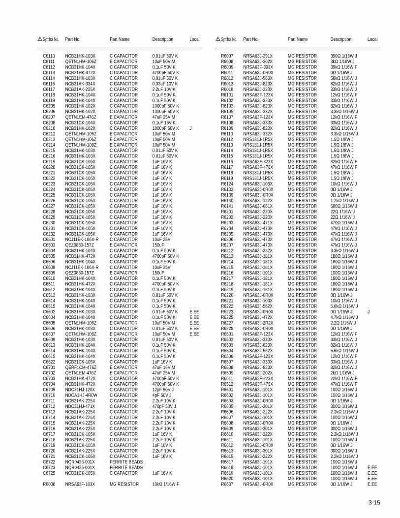
3-15
C6110 NCB31HK-103X C CAPACITOR 0.01uF 50V KC6111 QETN1HM-106Z E CAPACITOR 10uF 50V MC6112 NCB31HK-104X C CAPACITOR 0.1uF 50V KC6113 NCB31HK-472X C CAPACITOR 4700pF 50V KC6114 NCB31HK-103X C CAPACITOR 0.01uF 50V KC6115 NCB31AK-334X C CAPACITOR 0.33uF 10V KC6117 NCB21AK-225X C CAPACITOR 2.2uF 10V KC6118 NCB31HK-104X C CAPACITOR 0.1uF 50V KC6119 NCB31HK-104X C CAPACITOR 0.1uF 50V KC6205 NCB31HK-102X C CAPACITOR 1000pF 50V KC6206 NCB31HK-102X C CAPACITOR 1000pF 50V KC6207 QETN1EM-476Z E CAPACITOR 47uF 25V MC6208 NCB31CK-104X C CAPACITOR 0.1uF 16V KC6210 NCB31HK-102X C CAPACITOR 1000pF 50V K JC6212 QETN1HM-106Z E CAPACITOR 10uF 50V MC6213 QETN1HM-106Z E CAPACITOR 10uF 50V MC6214 QETN1HM-106Z E CAPACITOR 10uF 50V MC6215 NCB31HK-103X C CAPACITOR 0.01uF 50V KC6216 NCB31HK-103X C CAPACITOR 0.01uF 50V KC6219 NCB31CK-105X C CAPACITOR 1uF 16V KC6220 NCB31CK-105X C CAPACITOR 1uF 16V KC6221 NCB31CK-105X C CAPACITOR 1uF 16V KC6222 NCB31CK-105X C CAPACITOR 1uF 16V KC6223 NCB31CK-105X C CAPACITOR 1uF 16V KC6224 NCB31CK-105X C CAPACITOR 1uF 16V KC6225 NCB31CK-105X C CAPACITOR 1uF 16V KC6226 NCB31CK-105X C CAPACITOR 1uF 16V KC6227 NCB31CK-105X C CAPACITOR 1uF 16V KC6228 NCB31CK-105X C CAPACITOR 1uF 16V KC6229 NCB31CK-105X C CAPACITOR 1uF 16V KC6230 NCB31CK-105X C CAPACITOR 1uF 16V KC6231 NCB31CK-105X C CAPACITOR 1uF 16V KC6232 NCB31CK-105X C CAPACITOR 1uF 16V KC6501 NCJ11EK-106X-R C CAPACITOR 10uF 25VC6503 QEZ0850-157Z E CAPACITOR 150uFC6504 NCB31HK-104X C CAPACITOR 0.1uF 50V KC6505 NCB31HK-472X C CAPACITOR 4700pF 50V KC6506 NCB31HK-104X C CAPACITOR 0.1uF 50V KC6508 NCJ11EK-106X-R C CAPACITOR 10uF 25VC6509 QEZ0850-157Z E CAPACITOR 150uFC6510 NCB31HK-104X C CAPACITOR 0.1uF 50V KC6511 NCB31HK-472X C CAPACITOR 4700pF 50V KC6512 NCB31HK-104X C CAPACITOR 0.1uF 50V KC6513 NCB31HK-103X C CAPACITOR 0.01uF 50V KC6514 NCB31HK-104X C CAPACITOR 0.1uF 50V KC6515 NCB31HK-104X C CAPACITOR 0.1uF 50V KC6602 NCB31HK-103X C CAPACITOR 0.01uF 50V K E,EEC6604 NCB31HK-104X C CAPACITOR 0.1uF 50V K E,EEC6605 QETN1HM-106Z E CAPACITOR 10uF 50V M E,EEC6606 NCB31HK-103X C CAPACITOR 0.01uF 50V K E,EEC6607 QETN1HM-106Z E CAPACITOR 10uF 50V M E,EEC6609 NCB31HK-103X C CAPACITOR 0.01uF 50V KC6613 NCB31HK-104X C CAPACITOR 0.1uF 50V KC6614 NCB31HK-104X C CAPACITOR 0.1uF 50V KC6615 NCB31HK-104X C CAPACITOR 0.1uF 50V KC6622 NCB31CK-105X C CAPACITOR 1uF 16V KC6701 QERF1CM-476Z E CAPACITOR 47uF 16V MC6702 QETN1EM-476Z E CAPACITOR 47uF 25V MC6703 NCB31HK-472X C CAPACITOR 4700pF 50V KC6704 NCB31HK-472X C CAPACITOR 4700pF 50V KC6705 NDC31HJ-120X C CAPACITOR 12pF 50V JC6710 NDCA1HJ-4R0W C CAPACITOR 4pF 50V JC6711 NCB21AK-225X C CAPACITOR 2.2uF 10V KC6712 NDC31HJ-471X C CAPACITOR 470pF 50V JC6713 NCB21AK-225X C CAPACITOR 2.2uF 10V KC6714 NCB21AK-225X C CAPACITOR 2.2uF 10V KC6715 NCB21AK-225X C CAPACITOR 2.2uF 10V KC6716 NCB21AK-225X C CAPACITOR 2.2uF 10V KC6717 NCB31CK-105X C CAPACITOR 1uF 16V KC6718 NCB21AK-225X C CAPACITOR 2.2uF 10V KC6719 NCB31CK-105X C CAPACITOR 1uF 16V KC6720 NCB21AK-225X C CAPACITOR 2.2uF 10V KC6721 NCB31CK-105X C CAPACITOR 1uF 16V KC6722 NQR0436-001X FERRITE BEADSC6723 NQR0436-001X FERRITE BEADSC6725 NCB31CK-105X C CAPACITOR 1uF 16V K
R6006 NRSA63F-103X MG RESISTOR 10kΩ 1/16W F
Symbol No. Part No. Part Name Description Local
R6007 NRSA63J-391X MG RESISTOR 390Ω 1/16W JR6008 NRSA63J-302X MG RESISTOR 3kΩ 1/16W JR6009 NRSA63F-393X MG RESISTOR 39kΩ 1/16W FR6011 NRSA63J-0R0X MG RESISTOR 0Ω 1/16W JR6012 NRSA63J-563X MG RESISTOR 56kΩ 1/16W JR6013 NRSA63J-823X MG RESISTOR 82kΩ 1/16W JR6018 NRSA63J-333X MG RESISTOR 33kΩ 1/16W JR6101 NRSA63F-123X MG RESISTOR 12kΩ 1/16W FR6102 NRSA63J-333X MG RESISTOR 33kΩ 1/16W JR6103 NRSA63J-823X MG RESISTOR 82kΩ 1/16W JR6105 NRSA63J-332X MG RESISTOR 3.3kΩ 1/16W JR6107 NRSA63F-123X MG RESISTOR 12kΩ 1/16W FR6108 NRSA63J-333X MG RESISTOR 33kΩ 1/16W JR6109 NRSA63J-823X MG RESISTOR 82kΩ 1/16W JR6110 NRSA63J-332X MG RESISTOR 3.3kΩ 1/16W JR6112 NRS181J-1R5X MG RESISTOR 1.5Ω 1/8W JR6113 NRS181J-1R5X MG RESISTOR 1.5Ω 1/8W JR6114 NRS181J-1R5X MG RESISTOR 1.5Ω 1/8W JR6115 NRS181J-1R5X MG RESISTOR 1.5Ω 1/8W JR6116 NRSA63F-823X MG RESISTOR 82kΩ 1/16W FR6117 NRSA63F-473X MG RESISTOR 47kΩ 1/16W FR6118 NRS181J-1R5X MG RESISTOR 1.5Ω 1/8W JR6119 NRS181J-1R5X MG RESISTOR 1.5Ω 1/8W JR6124 NRSA63J-103X MG RESISTOR 10kΩ 1/16W JR6133 NRSA63J-0R0X MG RESISTOR 0Ω 1/16W JR6139 NRSA63J-0R0X MG RESISTOR 0Ω 1/16W JR6140 NRSA63J-122X MG RESISTOR 1.2kΩ 1/16W JR6141 NRSA63J-681X MG RESISTOR 680Ω 1/16W JR6201 NRSA63J-220X MG RESISTOR 22Ω 1/16W JR6202 NRSA63J-220X MG RESISTOR 22Ω 1/16W JR6203 NRSA63J-471X MG RESISTOR 470Ω 1/16W JR6204 NRSA63J-473X MG RESISTOR 47kΩ 1/16W JR6205 NRSA63J-473X MG RESISTOR 47kΩ 1/16W JR6206 NRSA63J-473X MG RESISTOR 47kΩ 1/16W JR6207 NRSA63J-473X MG RESISTOR 47kΩ 1/16W JR6212 NRSA63J-332X MG RESISTOR 3.3kΩ 1/16W JR6213 NRSA63J-181X MG RESISTOR 180Ω 1/16W JR6214 NRSA63J-181X MG RESISTOR 180Ω 1/16W JR6215 NRSA63J-181X MG RESISTOR 180Ω 1/16W JR6216 NRSA63J-101X MG RESISTOR 100Ω 1/16W JR6217 NRSA63J-181X MG RESISTOR 180Ω 1/16W JR6218 NRSA63J-181X MG RESISTOR 180Ω 1/16W JR6219 NRSA63J-181X MG RESISTOR 180Ω 1/16W JR6220 NRSA63J-0R0X MG RESISTOR 0Ω 1/16W JR6221 NRSA63J-103X MG RESISTOR 10kΩ 1/16W JR6222 NRSA63J-562X MG RESISTOR 5.6kΩ 1/16W JR6223 NRSA63J-0R0X MG RESISTOR 0Ω 1/16W J JR6225 NRSA63J-472X MG RESISTOR 4.7kΩ 1/16W JR6227 NRSA63J-2R2X MG RESISTOR 2.2Ω 1/16W JR6228 NRSA63J-0R0X MG RESISTOR 0Ω 1/16W JR6501 NRSA63F-123X MG RESISTOR 12kΩ 1/16W FR6502 NRSA63J-333X MG RESISTOR 33kΩ 1/16W JR6503 NRSA63J-823X MG RESISTOR 82kΩ 1/16W JR6504 NRSA63J-562X MG RESISTOR 5.6kΩ 1/16W JR6506 NRSA63F-123X MG RESISTOR 12kΩ 1/16W FR6507 NRSA63J-333X MG RESISTOR 33kΩ 1/16W JR6508 NRSA63J-823X MG RESISTOR 82kΩ 1/16W JR6509 NRSA63J-202X MG RESISTOR 2kΩ 1/16W JR6511 NRSA63F-223X MG RESISTOR 22kΩ 1/16W FR6512 NRSA63F-473X MG RESISTOR 47kΩ 1/16W FR6601 NRSA63J-101X MG RESISTOR 100Ω 1/16W JR6602 NRSA63J-101X MG RESISTOR 100Ω 1/16W JR6603 NRSA63J-0R0X MG RESISTOR 0Ω 1/16W JR6605 NRSA63J-301X MG RESISTOR 300Ω 1/16W JR6606 NRSA63J-222X MG RESISTOR 2.2kΩ 1/16W JR6607 NRSA63J-101X MG RESISTOR 100Ω 1/16W JR6608 NRSA63J-0R0X MG RESISTOR 0Ω 1/16W JR6609 NRSA63J-301X MG RESISTOR 300Ω 1/16W JR6610 NRSA63J-222X MG RESISTOR 2.2kΩ 1/16W JR6611 NRSA63J-101X MG RESISTOR 100Ω 1/16W JR6612 NRSA63J-0R0X MG RESISTOR 0Ω 1/16W JR6613 NRSA63J-301X MG RESISTOR 300Ω 1/16W JR6615 NRSA63J-222X MG RESISTOR 2.2kΩ 1/16W JR6617 NRSA63J-101X MG RESISTOR 100Ω 1/16W JR6618 NRSA63J-101X MG RESISTOR 100Ω 1/16W J E,EER6619 NRSA63J-101X MG RESISTOR 100Ω 1/16W J E,EER6620 NRSA63J-101X MG RESISTOR 100Ω 1/16W J E,EER6637 NRSA63J-0R0X MG RESISTOR 0Ω 1/16W J E,EE
Symbol No. Part No. Part Name Description Local
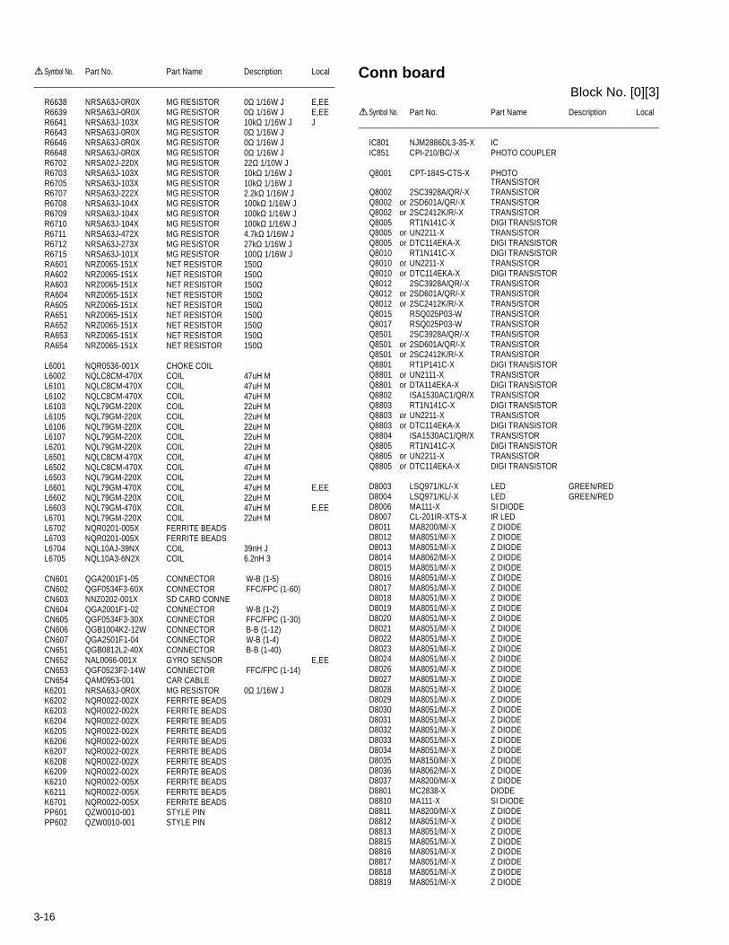
3-16
Conn boardBlock No. [0][3]
R6638 NRSA63J-0R0X MG RESISTOR 0Ω 1/16W J E,EER6639 NRSA63J-0R0X MG RESISTOR 0Ω 1/16W J E,EER6641 NRSA63J-103X MG RESISTOR 10kΩ 1/16W J JR6643 NRSA63J-0R0X MG RESISTOR 0Ω 1/16W JR6646 NRSA63J-0R0X MG RESISTOR 0Ω 1/16W JR6648 NRSA63J-0R0X MG RESISTOR 0Ω 1/16W JR6702 NRSA02J-220X MG RESISTOR 22Ω 1/10W JR6703 NRSA63J-103X MG RESISTOR 10kΩ 1/16W JR6705 NRSA63J-103X MG RESISTOR 10kΩ 1/16W JR6707 NRSA63J-222X MG RESISTOR 2.2kΩ 1/16W JR6708 NRSA63J-104X MG RESISTOR 100kΩ 1/16W JR6709 NRSA63J-104X MG RESISTOR 100kΩ 1/16W JR6710 NRSA63J-104X MG RESISTOR 100kΩ 1/16W JR6711 NRSA63J-472X MG RESISTOR 4.7kΩ 1/16W JR6712 NRSA63J-273X MG RESISTOR 27kΩ 1/16W JR6715 NRSA63J-101X MG RESISTOR 100Ω 1/16W JRA601 NRZ0065-151X NET RESISTOR 150ΩRA602 NRZ0065-151X NET RESISTOR 150ΩRA603 NRZ0065-151X NET RESISTOR 150ΩRA604 NRZ0065-151X NET RESISTOR 150ΩRA605 NRZ0065-151X NET RESISTOR 150ΩRA651 NRZ0065-151X NET RESISTOR 150ΩRA652 NRZ0065-151X NET RESISTOR 150ΩRA653 NRZ0065-151X NET RESISTOR 150ΩRA654 NRZ0065-151X NET RESISTOR 150Ω
L6001 NQR0536-001X CHOKE COILL6002 NQLC8CM-470X COIL 47uH ML6101 NQLC8CM-470X COIL 47uH ML6102 NQLC8CM-470X COIL 47uH ML6103 NQL79GM-220X COIL 22uH ML6105 NQL79GM-220X COIL 22uH ML6106 NQL79GM-220X COIL 22uH ML6107 NQL79GM-220X COIL 22uH ML6201 NQL79GM-220X COIL 22uH ML6501 NQLC8CM-470X COIL 47uH ML6502 NQLC8CM-470X COIL 47uH ML6503 NQL79GM-220X COIL 22uH ML6601 NQL79GM-470X COIL 47uH M E,EEL6602 NQL79GM-220X COIL 22uH ML6603 NQL79GM-470X COIL 47uH M E,EEL6701 NQL79GM-220X COIL 22uH ML6702 NQR0201-005X FERRITE BEADSL6703 NQR0201-005X FERRITE BEADSL6704 NQL10AJ-39NX COIL 39nH JL6705 NQL10A3-6N2X COIL 6.2nH 3
CN601 QGA2001F1-05 CONNECTOR W-B (1-5)CN602 QGF0534F3-60X CONNECTOR FFC/FPC (1-60)CN603 NNZ0202-001X SD CARD CONNECN604 QGA2001F1-02 CONNECTOR W-B (1-2)CN605 QGF0534F3-30X CONNECTOR FFC/FPC (1-30)CN606 QGB1004K2-12W CONNECTOR B-B (1-12)CN607 QGA2501F1-04 CONNECTOR W-B (1-4)CN651 QGB0812L2-40X CONNECTOR B-B (1-40)CN652 NAL0066-001X GYRO SENSOR E,EECN653 QGF0523F2-14W CONNECTOR FFC/FPC (1-14)CN654 QAM0953-001 CAR CABLEK6201 NRSA63J-0R0X MG RESISTOR 0Ω 1/16W JK6202 NQR0022-002X FERRITE BEADSK6203 NQR0022-002X FERRITE BEADSK6204 NQR0022-002X FERRITE BEADSK6205 NQR0022-002X FERRITE BEADSK6206 NQR0022-002X FERRITE BEADSK6207 NQR0022-002X FERRITE BEADSK6208 NQR0022-002X FERRITE BEADSK6209 NQR0022-002X FERRITE BEADSK6210 NQR0022-005X FERRITE BEADSK6211 NQR0022-005X FERRITE BEADSK6701 NQR0022-005X FERRITE BEADSPP601 QZW0010-001 STYLE PINPP602 QZW0010-001 STYLE PIN
Symbol No. Part No. Part Name Description Local
Symbol No. Part No. Part Name Description Local
IC801 NJM2886DL3-35-X ICIC851 CPI-210/BC/-X PHOTO COUPLER
Q8001 CPT-184S-CTS-X PHOTO TRANSISTOR
Q8002 2SC3928A/QR/-X TRANSISTORQ8002 or 2SD601A/QR/-X TRANSISTORQ8002 or 2SC2412K/R/-X TRANSISTORQ8005 RT1N141C-X DIGI TRANSISTORQ8005 or UN2211-X TRANSISTORQ8005 or DTC114EKA-X DIGI TRANSISTORQ8010 RT1N141C-X DIGI TRANSISTORQ8010 or UN2211-X TRANSISTORQ8010 or DTC114EKA-X DIGI TRANSISTORQ8012 2SC3928A/QR/-X TRANSISTORQ8012 or 2SD601A/QR/-X TRANSISTORQ8012 or 2SC2412K/R/-X TRANSISTORQ8015 RSQ025P03-W TRANSISTORQ8017 RSQ025P03-W TRANSISTORQ8501 2SC3928A/QR/-X TRANSISTORQ8501 or 2SD601A/QR/-X TRANSISTORQ8501 or 2SC2412K/R/-X TRANSISTORQ8801 RT1P141C-X DIGI TRANSISTORQ8801 or UN2111-X TRANSISTORQ8801 or DTA114EKA-X DIGI TRANSISTORQ8802 ISA1530AC1/QR/X TRANSISTORQ8803 RT1N141C-X DIGI TRANSISTORQ8803 or UN2211-X TRANSISTORQ8803 or DTC114EKA-X DIGI TRANSISTORQ8804 ISA1530AC1/QR/X TRANSISTORQ8805 RT1N141C-X DIGI TRANSISTORQ8805 or UN2211-X TRANSISTORQ8805 or DTC114EKA-X DIGI TRANSISTOR
D8003 LSQ971/KL/-X LED GREEN/REDD8004 LSQ971/KL/-X LED GREEN/REDD8006 MA111-X SI DIODED8007 CL-201IR-XTS-X IR LEDD8011 MA8200/M/-X Z DIODED8012 MA8051/M/-X Z DIODED8013 MA8051/M/-X Z DIODED8014 MA8062/M/-X Z DIODED8015 MA8051/M/-X Z DIODED8016 MA8051/M/-X Z DIODED8017 MA8051/M/-X Z DIODED8018 MA8051/M/-X Z DIODED8019 MA8051/M/-X Z DIODED8020 MA8051/M/-X Z DIODED8021 MA8051/M/-X Z DIODED8022 MA8051/M/-X Z DIODED8023 MA8051/M/-X Z DIODED8024 MA8051/M/-X Z DIODED8026 MA8051/M/-X Z DIODED8027 MA8051/M/-X Z DIODED8028 MA8051/M/-X Z DIODED8029 MA8051/M/-X Z DIODED8030 MA8051/M/-X Z DIODED8031 MA8051/M/-X Z DIODED8032 MA8051/M/-X Z DIODED8033 MA8051/M/-X Z DIODED8034 MA8051/M/-X Z DIODED8035 MA8150/M/-X Z DIODED8036 MA8062/M/-X Z DIODED8037 MA8200/M/-X Z DIODED8801 MC2838-X DIODED8810 MA111-X SI DIODED8811 MA8200/M/-X Z DIODED8812 MA8051/M/-X Z DIODED8813 MA8051/M/-X Z DIODED8815 MA8051/M/-X Z DIODED8816 MA8051/M/-X Z DIODED8817 MA8051/M/-X Z DIODED8818 MA8051/M/-X Z DIODED8819 MA8051/M/-X Z DIODE

3-17
Panel boardBlock No. [0][4]
D8820 MA8051/M/-X Z DIODED8821 MA8051/M/-X Z DIODED8822 MA8051/M/-X Z DIODED8823 MA8051/M/-X Z DIODED8824 MA8051/M/-X Z DIODED8826 MA8051/M/-X Z DIODED8827 MA8051/M/-X Z DIODED8828 MA8051/M/-X Z DIODED8829 MA8150/M/-X Z DIODED8830 MA8200/M/-X Z DIODED8831 MA8051/M/-X Z DIODED8832 MA8051/M/-X Z DIODED8833 MA8051/M/-X Z DIODED8834 MA8051/M/-X Z DIODED8835 MA8051/M/-X Z DIODED8836 MA8062/M/-X Z DIODE
C8003 NCJ11EK-106X-R C CAPACITOR 10uF 25VC8004 NCJ11EK-106X-R C CAPACITOR 10uF 25VC8005 NCB31AK-334X C CAPACITOR 0.33uF 10V KC8006 NCJ11EK-106X-R C CAPACITOR 10uF 25VC8010 NCB31HK-103X C CAPACITOR 0.01uF 50V KC8011 NCB21AK-225X C CAPACITOR 2.2uF 10V K
R8001 NRSA63J-333X MG RESISTOR 33kΩ 1/16W JR8002 NRSA63J-103X MG RESISTOR 10kΩ 1/16W JR8003 NRSA63J-333X MG RESISTOR 33kΩ 1/16W JR8004 NRSA63J-333X MG RESISTOR 33kΩ 1/16W JR8005 NRSA63J-101X MG RESISTOR 100Ω 1/16W JR8015 NRSA63J-0R0X MG RESISTOR 0Ω 1/16W JR8017 NRSA63J-0R0X MG RESISTOR 0Ω 1/16W JR8018 NRSA63J-0R0X MG RESISTOR 0Ω 1/16W JR8019 NRSA63J-0R0X MG RESISTOR 0Ω 1/16W JR8021 NRSA63J-103X MG RESISTOR 10kΩ 1/16W JR8024 NRSA63J-0R0X MG RESISTOR 0Ω 1/16W JR8025 NRSA63J-103X MG RESISTOR 10kΩ 1/16W JR8029 NRSA63J-103X MG RESISTOR 10kΩ 1/16W JR8030 NRSA63J-682X MG RESISTOR 6.8kΩ 1/16W JR8031 NRSA63J-391X MG RESISTOR 390Ω 1/16W JR8032 NRSA63J-682X MG RESISTOR 6.8kΩ 1/16W JR8034 NRSA63J-682X MG RESISTOR 6.8kΩ 1/16W JR8038 NRSA63J-0R0X MG RESISTOR 0Ω 1/16W JR8041 NRSA63J-0R0X MG RESISTOR 0Ω 1/16W JR8042 NRSA63J-0R0X MG RESISTOR 0Ω 1/16W JR8046 NRSA63J-682X MG RESISTOR 6.8kΩ 1/16W JR8047 NRSA63J-682X MG RESISTOR 6.8kΩ 1/16W JR8501 NRSA63J-751X MG RESISTOR 750Ω 1/16W JR8503 NRSA63J-393X MG RESISTOR 39kΩ 1/16W JR8504 NRSA63J-333X MG RESISTOR 33kΩ 1/16W JR8505 NRSA63J-333X MG RESISTOR 33kΩ 1/16W JR8507 NRSA63J-682X MG RESISTOR 6.8kΩ 1/16W JR8508 NRSA63J-222X MG RESISTOR 2.2kΩ 1/16W JR8509 NRSA63J-102X MG RESISTOR 1kΩ 1/16W JR8510 NRSA63J-151X MG RESISTOR 150Ω 1/16W JR8511 NRSA63J-0R0X MG RESISTOR 0Ω 1/16W JR8801 NRSA63J-0R0X MG RESISTOR 0Ω 1/16W JR8802 NRSA63J-0R0X MG RESISTOR 0Ω 1/16W JR8803 NRSA63J-0R0X MG RESISTOR 0Ω 1/16W JR8805 NRSA63J-222X MG RESISTOR 2.2kΩ 1/16W JR8811 NRSA63J-471X MG RESISTOR 470Ω 1/16W J JR8811 NRSA63J-681X MG RESISTOR 680Ω 1/16W J E,EER8812 NRSA63J-562X MG RESISTOR 5.6kΩ 1/16W J JR8812 NRSA63J-113X MG RESISTOR 11kΩ 1/16W J E,EER8813 NRSA63J-562X MG RESISTOR 5.6kΩ 1/16W J JR8813 NRSA63J-113X MG RESISTOR 11kΩ 1/16W J E,EER8815 NRSA63J-473X MG RESISTOR 47kΩ 1/16W JR8816 NRSA63J-562X MG RESISTOR 5.6kΩ 1/16W JR8817 NRSA63J-473X MG RESISTOR 47kΩ 1/16W JR8818 NRSA63J-562X MG RESISTOR 5.6kΩ 1/16W JR8819 NRSA63J-182X MG RESISTOR 1.8kΩ 1/16W J JR8819 NRSA63J-362X MG RESISTOR 3.6kΩ 1/16W J E,EER8820 NRSA63J-272X MG RESISTOR 2.7kΩ 1/16W J JR8820 NRSA63J-392X MG RESISTOR 3.9kΩ 1/16W J E,EER8821 NRSA63J-332X MG RESISTOR 3.3kΩ 1/16W J JR8821 NRSA63J-362X MG RESISTOR 3.6kΩ 1/16W J E,EER8822 NRSA63J-332X MG RESISTOR 3.3kΩ 1/16W J JR8823 NRSA63J-332X MG RESISTOR 3.3kΩ 1/16W J JR8823 NRSA63J-472X MG RESISTOR 4.7kΩ 1/16W J E,EE
Symbol No. Part No. Part Name Description Local
R8824 NRSA63J-182X MG RESISTOR 1.8kΩ 1/16W J JR8824 NRSA63J-362X MG RESISTOR 3.6kΩ 1/16W J E,EER8825 NRSA63J-272X MG RESISTOR 2.7kΩ 1/16W J JR8825 NRSA63J-392X MG RESISTOR 3.9kΩ 1/16W J E,EE
L8001 NQL52EM-220X COIL 22uH M
CN801 QGB1004J2-12X CONNECTOR B-B (1-12)CN802 QGB1004J2-30X CONNECTOR B-B (1-30)CN803 QGF0567F1-24W CONNECTOR FFC/FPC (1-24)CN804 QGF0567F1-24W CONNECTOR FFC/FPC (1-24)CN851 QGA1002C1-06X CONNECTOR W-B (1-6)CN852 QGA1002C1-02X CONNECTOR W-B (1-2)CN881 QGF0534F3-60X CONNECTOR FFC/FPC (1-60)CN882 QGZ2204M1-24X CONNECTOR (1-24)CN883 QGZ2204M1-24X CONNECTOR (1-24)S8501 NSW0225-001X DETECT SWITCHS8502 NSW0126-001X DETECT SWITCHS8801 NSW0225-001X DETECT SWITCH
Symbol No. Part No. Part Name Description Local
IC402 NJM072BV-X ICIC411 TC74VHCT04AFT-X ICIC412 TC7W04FK-X IC
IC451 UPD78F0515GA4A IC(PROGRAMED)IC452 S-80824CNNB-G-W ICIC461 OZ964ISN-X ICIC462 TC7SET08FU-J-X IC(DIGITAL)IC463 TPCP8402JVC-X POWER MOS FETIC464 TPCP8402JVC-X POWER MOS FETIC471 AD9980KSTZ-80 ICIC472 NJM2878F3-18-X ICIC473 TC7SH08FU-X IC
IC501 MN103SE60P ICIC502 NJU6368PF1-X ICIC503 TC7SH04FU-X ICIC504 TC7PA14FU-X IC
IC511 K4S641632K-UC75 IC IC512 SG32N90TFI036F IC(PROGRAMED) J IC512 SG32N90TFI034H IC(PROGRAMED) E IC512 SG32N90TFI034J IC(PROGRAMED) EE
IC513 NJM2904V-X ICIC551 RS-771-X RM.RECEIVER
Q401 ISA1530AC1/QR/X TRANSISTORQ402 2SC3928A/QR/-X TRANSISTORQ402 or 2SD601A/QR/-X TRANSISTORQ402 or 2SC2412K/R/-X TRANSISTORQ403 RT1N141C-X DIGI TRANSISTORQ403 or UN2211-X TRANSISTORQ403 or DTC114EKA-X DIGI TRANSISTORQ506 2SC3928A/QR/-X TRANSISTORQ506 or 2SD601A/QR/-X TRANSISTORQ506 or 2SC2412K/R/-X TRANSISTORQ507 RT1N141C-X DIGI TRANSISTORQ507 or UN2211-X TRANSISTORQ507 or DTC114EKA-X DIGI TRANSISTORQ508 2SA2119K-X TRANSISTORQ509 2SA2119K-X TRANSISTORQ510 2SC5938A/B/-X TRANSISTORQ511 2SC5938A/B/-X TRANSISTORQ4001 2SC3928A/QR/-X TRANSISTORQ4001 or 2SD601A/QR/-X TRANSISTORQ4001 or 2SC2412K/R/-X TRANSISTORQ4002 ISA1530AC1/QR/X TRANSISTORQ4003 2SC3928A/QR/-X TRANSISTORQ4003 or 2SD601A/QR/-X TRANSISTORQ4003 or 2SC2412K/R/-X TRANSISTORQ4004 2SC3928A/QR/-X TRANSISTORQ4004 or 2SD601A/QR/-X TRANSISTOR
Symbol No. Part No. Part Name Description Local

3-18
Q4004 or 2SC2412K/R/-X TRANSISTORQ4005 ISA1530AC1/QR/X TRANSISTORQ4006 ISA1530AC1/QR/X TRANSISTORQ4007 2SC3928A/QR/-X TRANSISTORQ4007 or 2SD601A/QR/-X TRANSISTORQ4007 or 2SC2412K/R/-X TRANSISTORQ4605 ISA1530AC1/QR/X TRANSISTORQ4607 RT1N141C-X DIGI TRANSISTORQ4607 or UN2211-X TRANSISTORQ4607 or DTC114EKA-X DIGI TRANSISTORQ5001 ISA1530AC1/QR/X TRANSISTOR
D401 MA111-X SI DIODED402 MC2836-X DIODED506 MA111-X SI DIODED507 MA111-X SI DIODED508 MA8120/M/-X Z DIODED509 MA8120/M/-X Z DIODED551 CL-201IR-X-X LEDD552 NECBB205/WPQR/X LED JD552 SMLE12WBC7W-X LED E,EED553 NECBB205/WPQR/X LED JD553 SMLE12WBC7W-X LED E,EED554 NECBB205/WPQR/X LED JD554 SMLE12WBC7W-X LED E,EED555 NECBB205/WPQR/X LED JD555 SMLE12WBC7W-X LED E,EED556 NECBB205/WPQR/X LED JD556 SMLE12WBC7W-X LED E,EED557 NECBB205/WPQR/X LED JD557 SMLE12WBC7W-X LED E,EED558 NECBB205/WPQR/X LED JD558 SMLE12WBC7W-X LED E,EED559 NECBB205/WPQR/X LED JD559 SMLE12WBC7W-X LED E,EED560 NECBB205/WPQR/X LED JD560 SMLE12WBC7W-X LED E,EED561 NECBB205/WPQR/X LED JD561 SMLE12WBC7W-X LED E,EED562 NECBB205/WPQR/X LED JD562 SMLE12WBC7W-X LED E,EED563 NECBB205/WPQR/X LED JD563 SMLE12WBC7W-X LED E,EED4001 MA2SD32-X DIODED4301 MA2SD31-X SB DIODED4302 MA2SD31-X SB DIODED4303 MA8062/M/-X Z DIODED4601 MA111-X SI DIODED4602 MA8047/M/-X Z DIODED4603 MA8047/M/-X Z DIODED4604 BAV99L-X SI DIODED4605 MA8047/M/-X Z DIODED4606 MA8047/M/-X Z DIODED4607 BAV99L-X SI DIODED5001 MA2SD31-X SB DIODED5002 MA2SD31-X SB DIODE
C401 NCB30JK-105X C CAPACITOR 1uF 6.3V KC402 NBE40JM-476X TA E CAPACITOR 47uF 6.3V MC403 NDCA1HJ-101W C CAPACITOR 100pF 50V JC404 NDCA1HJ-101W C CAPACITOR 100pF 50V JC405 NCB31CK-473X C CAPACITOR 0.047uF 16V KC406 NCBA1AK-473W C CAPACITOR 0.047uF 10V KC407 NDCA1HJ-5R0W C CAPACITOR 5pF 50V JC408 NDCA1HJ-5R0W C CAPACITOR 5pF 50V JC409 NCB31AK-474X C CAPACITOR 0.47uF 10V KC410 NCB30JK-105X C CAPACITOR 1uF 6.3V KC411 NCBA1CK-103W C CAPACITOR 0.01uF 16V KC412 NCB20JK-475X C CAPACITOR 4.7uF 6.3V KC413 NCBA1AK-473W C CAPACITOR 0.047uF 10V KC422 NRSA63J-0R0X MG RESISTOR 0Ω 1/16W JC428 NRSA63J-0R0X MG RESISTOR 0Ω 1/16W JC429 NRSA63J-0R0X MG RESISTOR 0Ω 1/16W JC430 NRSA63J-0R0X MG RESISTOR 0Ω 1/16W JC431 NRSA63J-0R0X MG RESISTOR 0Ω 1/16W JC437 NCB31HK-102X C CAPACITOR 1000pF 50V KC438 NCB31HK-102X C CAPACITOR 1000pF 50V KC501 NCB20JK-475X C CAPACITOR 4.7uF 6.3V K
Symbol No. Part No. Part Name Description Local
C502 NCB31HK-104X C CAPACITOR 0.1uF 50V KC503 NCB31AK-474X C CAPACITOR 0.47uF 10V KC504 NCB31AK-474X C CAPACITOR 0.47uF 10V KC505 NCJ11EK-106X-R C CAPACITOR 10uF 25VC507 NCB31HK-102X C CAPACITOR 1000pF 50V KC508 NCB31HK-102X C CAPACITOR 1000pF 50V KC509 NDC31HJ-101X C CAPACITOR 100pF 50V JC510 NDC31HJ-101X C CAPACITOR 100pF 50V JC511 NDC31HJ-101X C CAPACITOR 100pF 50V JC512 NDC31HJ-101X C CAPACITOR 100pF 50V JC513 NCBA1HK-102W C CAPACITOR 1000pF 50V KC514 NCBA1HK-102W C CAPACITOR 1000pF 50V KC552 NCBA1AK-104W C CAPACITOR 0.1uF 10V KC553 NCBA1HK-102W C CAPACITOR 1000pF 50V KC4001 NCB31AK-474X C CAPACITOR 0.47uF 10V KC4002 NCB31AK-474X C CAPACITOR 0.47uF 10V KC4003 NCB31AK-474X C CAPACITOR 0.47uF 10V KC4004 NCB31AK-474X C CAPACITOR 0.47uF 10V KC4006 NCJ11EK-106X-R C CAPACITOR 10uF 25VC4008 NCB31CK-105X C CAPACITOR 1uF 16V KC4009 NCB31CK-104X C CAPACITOR 0.1uF 16V KC4010 NCJ21CK-106X-R C CAPACITOR 10uF 16V KC4012 NCB31CK-105X C CAPACITOR 1uF 16V KC4013 NCBA1AK-104W C CAPACITOR 0.1uF 10V KC4015 NCB31CK-104X C CAPACITOR 0.1uF 16V KC4016 NCJ21CK-106X-R C CAPACITOR 10uF 16V KC4017 NCBA1AK-104W C CAPACITOR 0.1uF 10V KC4101 NCB31CK-104X C CAPACITOR 0.1uF 16V KC4102 NCB31CK-104X C CAPACITOR 0.1uF 16V KC4301 NQR0450-001X EMI FILTER 0.022uF 50V MC4302 NQR0450-001X EMI FILTER 0.022uF 50V MC4303 NCB31CK-104X C CAPACITOR 0.1uF 16V KC4304 NCB31HK-104X C CAPACITOR 0.1uF 50V KC4305 NCBA1AK-104W C CAPACITOR 0.1uF 10V KC4306 NCBA1AK-104W C CAPACITOR 0.1uF 10V KC4307 NBE41AM-476X TA E CAPACITOR 47uF 10V MC4308 NBE20JM-476X TA E CAPACITOR 47uF 6.3V MC4309 NCJ11EK-106X-R C CAPACITOR 10uF 25VC4310 NCJ11EK-106X-R C CAPACITOR 10uF 25VC4311 NCJ21CK-106X-R C CAPACITOR 10uF 16V KC4601 NQR0450-001X EMI FILTER 0.022uF 50V MC4602 NCB30JK-105X C CAPACITOR 1uF 6.3V KC4603 NCBA1AK-104W C CAPACITOR 0.1uF 10V KC4605 NCB21AK-225X C CAPACITOR 2.2uF 10V KC4606 NCBA1CK-103W C CAPACITOR 0.01uF 16V KC4607 NCB31AK-474X C CAPACITOR 0.47uF 10V KC4608 NCBA1AK-104W C CAPACITOR 0.1uF 10V KC4609 NDCA1HJ-101W C CAPACITOR 100pF 50V JC4610 NCBA1AK-104W C CAPACITOR 0.1uF 10V KC4611 NCB31HK-473X C CAPACITOR 0.047uF 50V KC4613 NDCA1HJ-101W C CAPACITOR 100pF 50V JC4614 NDCA1HJ-101W C CAPACITOR 100pF 50V JC4615 NDC31HJ-221X C CAPACITOR 220pF 50V JC4616 NDCA1HJ-101W C CAPACITOR 100pF 50V JC4617 NDCA1HJ-101W C CAPACITOR 100pF 50V JC4618 NCB31HK-473X C CAPACITOR 0.047uF 50V KC4619 NCB31HK-473X C CAPACITOR 0.047uF 50V KC4620 NCJ11EK-106X-R C CAPACITOR 10uF 25VC4621 NCF21HZ-105X C CAPACITOR 1uF 50V ZC4622 NCF21HZ-105X C CAPACITOR 1uF 50V ZC4623 NCJ11EK-106X-R C CAPACITOR 10uF 25VC4624 NCJ11EK-106X-R C CAPACITOR 10uF 25VC4625 NCJ11EK-106X-R C CAPACITOR 10uF 25VC4626 NCJ11EK-106X-R C CAPACITOR 10uF 25VC4627 NCJ11EK-106X-R C CAPACITOR 10uF 25VC4628 NCB11CK-225X C CAPACITOR 2.2uF 16V KC4629 NCB31HK-473X C CAPACITOR 0.047uF 50V KC4630 NCB31HK-333X C CAPACITOR 0.033uF 50V KC4631 NCZ1011-220X C CAPACITOR 22pFC4632 NCB31HK-392X C CAPACITOR 3900pF 50V KC4635 NDC31HJ-101X C CAPACITOR 100pF 50V J JC4701 NBE20JM-226X TA E CAPACITOR 22uF 6.3V MC4702 NCBA1AK-104W C CAPACITOR 0.1uF 10V KC4703 NCBA1AK-104W C CAPACITOR 0.1uF 10V KC4704 NCBA1AK-104W C CAPACITOR 0.1uF 10V KC4705 NCBA1AK-104W C CAPACITOR 0.1uF 10V KC4706 NCBA1AK-104W C CAPACITOR 0.1uF 10V KC4707 NCBA1AK-104W C CAPACITOR 0.1uF 10V K
Symbol No. Part No. Part Name Description Local
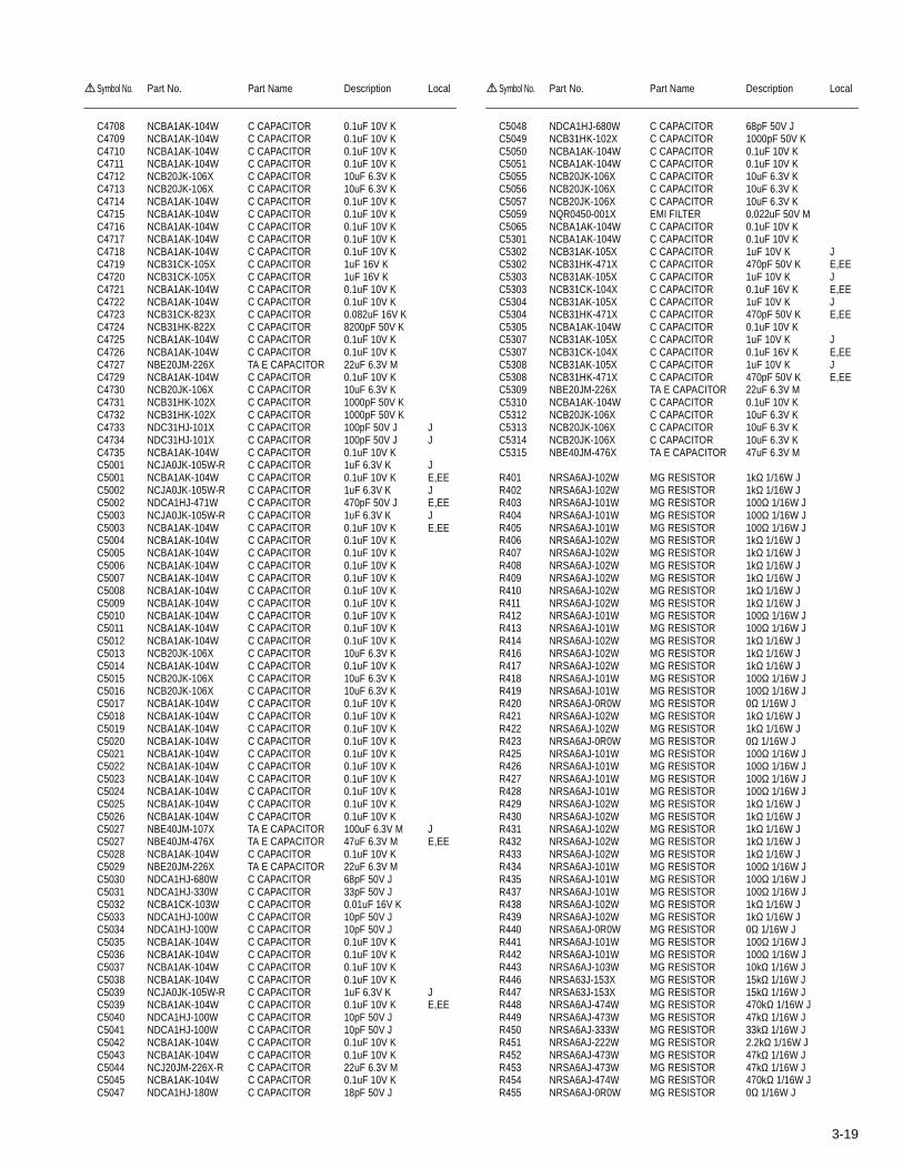
3-19
C4708 NCBA1AK-104W C CAPACITOR 0.1uF 10V KC4709 NCBA1AK-104W C CAPACITOR 0.1uF 10V KC4710 NCBA1AK-104W C CAPACITOR 0.1uF 10V KC4711 NCBA1AK-104W C CAPACITOR 0.1uF 10V KC4712 NCB20JK-106X C CAPACITOR 10uF 6.3V KC4713 NCB20JK-106X C CAPACITOR 10uF 6.3V KC4714 NCBA1AK-104W C CAPACITOR 0.1uF 10V KC4715 NCBA1AK-104W C CAPACITOR 0.1uF 10V KC4716 NCBA1AK-104W C CAPACITOR 0.1uF 10V KC4717 NCBA1AK-104W C CAPACITOR 0.1uF 10V KC4718 NCBA1AK-104W C CAPACITOR 0.1uF 10V KC4719 NCB31CK-105X C CAPACITOR 1uF 16V KC4720 NCB31CK-105X C CAPACITOR 1uF 16V KC4721 NCBA1AK-104W C CAPACITOR 0.1uF 10V KC4722 NCBA1AK-104W C CAPACITOR 0.1uF 10V KC4723 NCB31CK-823X C CAPACITOR 0.082uF 16V KC4724 NCB31HK-822X C CAPACITOR 8200pF 50V KC4725 NCBA1AK-104W C CAPACITOR 0.1uF 10V KC4726 NCBA1AK-104W C CAPACITOR 0.1uF 10V KC4727 NBE20JM-226X TA E CAPACITOR 22uF 6.3V MC4729 NCBA1AK-104W C CAPACITOR 0.1uF 10V KC4730 NCB20JK-106X C CAPACITOR 10uF 6.3V KC4731 NCB31HK-102X C CAPACITOR 1000pF 50V KC4732 NCB31HK-102X C CAPACITOR 1000pF 50V KC4733 NDC31HJ-101X C CAPACITOR 100pF 50V J JC4734 NDC31HJ-101X C CAPACITOR 100pF 50V J JC4735 NCBA1AK-104W C CAPACITOR 0.1uF 10V KC5001 NCJA0JK-105W-R C CAPACITOR 1uF 6.3V K JC5001 NCBA1AK-104W C CAPACITOR 0.1uF 10V K E,EEC5002 NCJA0JK-105W-R C CAPACITOR 1uF 6.3V K JC5002 NDCA1HJ-471W C CAPACITOR 470pF 50V J E,EEC5003 NCJA0JK-105W-R C CAPACITOR 1uF 6.3V K JC5003 NCBA1AK-104W C CAPACITOR 0.1uF 10V K E,EEC5004 NCBA1AK-104W C CAPACITOR 0.1uF 10V KC5005 NCBA1AK-104W C CAPACITOR 0.1uF 10V KC5006 NCBA1AK-104W C CAPACITOR 0.1uF 10V KC5007 NCBA1AK-104W C CAPACITOR 0.1uF 10V KC5008 NCBA1AK-104W C CAPACITOR 0.1uF 10V KC5009 NCBA1AK-104W C CAPACITOR 0.1uF 10V KC5010 NCBA1AK-104W C CAPACITOR 0.1uF 10V KC5011 NCBA1AK-104W C CAPACITOR 0.1uF 10V KC5012 NCBA1AK-104W C CAPACITOR 0.1uF 10V KC5013 NCB20JK-106X C CAPACITOR 10uF 6.3V KC5014 NCBA1AK-104W C CAPACITOR 0.1uF 10V KC5015 NCB20JK-106X C CAPACITOR 10uF 6.3V KC5016 NCB20JK-106X C CAPACITOR 10uF 6.3V KC5017 NCBA1AK-104W C CAPACITOR 0.1uF 10V KC5018 NCBA1AK-104W C CAPACITOR 0.1uF 10V KC5019 NCBA1AK-104W C CAPACITOR 0.1uF 10V KC5020 NCBA1AK-104W C CAPACITOR 0.1uF 10V KC5021 NCBA1AK-104W C CAPACITOR 0.1uF 10V KC5022 NCBA1AK-104W C CAPACITOR 0.1uF 10V KC5023 NCBA1AK-104W C CAPACITOR 0.1uF 10V KC5024 NCBA1AK-104W C CAPACITOR 0.1uF 10V KC5025 NCBA1AK-104W C CAPACITOR 0.1uF 10V KC5026 NCBA1AK-104W C CAPACITOR 0.1uF 10V KC5027 NBE40JM-107X TA E CAPACITOR 100uF 6.3V M JC5027 NBE40JM-476X TA E CAPACITOR 47uF 6.3V M E,EEC5028 NCBA1AK-104W C CAPACITOR 0.1uF 10V KC5029 NBE20JM-226X TA E CAPACITOR 22uF 6.3V MC5030 NDCA1HJ-680W C CAPACITOR 68pF 50V JC5031 NDCA1HJ-330W C CAPACITOR 33pF 50V JC5032 NCBA1CK-103W C CAPACITOR 0.01uF 16V KC5033 NDCA1HJ-100W C CAPACITOR 10pF 50V JC5034 NDCA1HJ-100W C CAPACITOR 10pF 50V JC5035 NCBA1AK-104W C CAPACITOR 0.1uF 10V KC5036 NCBA1AK-104W C CAPACITOR 0.1uF 10V KC5037 NCBA1AK-104W C CAPACITOR 0.1uF 10V KC5038 NCBA1AK-104W C CAPACITOR 0.1uF 10V KC5039 NCJA0JK-105W-R C CAPACITOR 1uF 6.3V K JC5039 NCBA1AK-104W C CAPACITOR 0.1uF 10V K E,EEC5040 NDCA1HJ-100W C CAPACITOR 10pF 50V JC5041 NDCA1HJ-100W C CAPACITOR 10pF 50V JC5042 NCBA1AK-104W C CAPACITOR 0.1uF 10V KC5043 NCBA1AK-104W C CAPACITOR 0.1uF 10V KC5044 NCJ20JM-226X-R C CAPACITOR 22uF 6.3V MC5045 NCBA1AK-104W C CAPACITOR 0.1uF 10V KC5047 NDCA1HJ-180W C CAPACITOR 18pF 50V J
Symbol No. Part No. Part Name Description Local
C5048 NDCA1HJ-680W C CAPACITOR 68pF 50V JC5049 NCB31HK-102X C CAPACITOR 1000pF 50V KC5050 NCBA1AK-104W C CAPACITOR 0.1uF 10V KC5051 NCBA1AK-104W C CAPACITOR 0.1uF 10V KC5055 NCB20JK-106X C CAPACITOR 10uF 6.3V KC5056 NCB20JK-106X C CAPACITOR 10uF 6.3V KC5057 NCB20JK-106X C CAPACITOR 10uF 6.3V KC5059 NQR0450-001X EMI FILTER 0.022uF 50V MC5065 NCBA1AK-104W C CAPACITOR 0.1uF 10V KC5301 NCBA1AK-104W C CAPACITOR 0.1uF 10V KC5302 NCB31AK-105X C CAPACITOR 1uF 10V K JC5302 NCB31HK-471X C CAPACITOR 470pF 50V K E,EEC5303 NCB31AK-105X C CAPACITOR 1uF 10V K JC5303 NCB31CK-104X C CAPACITOR 0.1uF 16V K E,EEC5304 NCB31AK-105X C CAPACITOR 1uF 10V K JC5304 NCB31HK-471X C CAPACITOR 470pF 50V K E,EEC5305 NCBA1AK-104W C CAPACITOR 0.1uF 10V KC5307 NCB31AK-105X C CAPACITOR 1uF 10V K JC5307 NCB31CK-104X C CAPACITOR 0.1uF 16V K E,EEC5308 NCB31AK-105X C CAPACITOR 1uF 10V K JC5308 NCB31HK-471X C CAPACITOR 470pF 50V K E,EEC5309 NBE20JM-226X TA E CAPACITOR 22uF 6.3V MC5310 NCBA1AK-104W C CAPACITOR 0.1uF 10V KC5312 NCB20JK-106X C CAPACITOR 10uF 6.3V KC5313 NCB20JK-106X C CAPACITOR 10uF 6.3V KC5314 NCB20JK-106X C CAPACITOR 10uF 6.3V KC5315 NBE40JM-476X TA E CAPACITOR 47uF 6.3V M
R401 NRSA6AJ-102W MG RESISTOR 1kΩ 1/16W JR402 NRSA6AJ-102W MG RESISTOR 1kΩ 1/16W JR403 NRSA6AJ-101W MG RESISTOR 100Ω 1/16W JR404 NRSA6AJ-101W MG RESISTOR 100Ω 1/16W JR405 NRSA6AJ-101W MG RESISTOR 100Ω 1/16W JR406 NRSA6AJ-102W MG RESISTOR 1kΩ 1/16W JR407 NRSA6AJ-102W MG RESISTOR 1kΩ 1/16W JR408 NRSA6AJ-102W MG RESISTOR 1kΩ 1/16W JR409 NRSA6AJ-102W MG RESISTOR 1kΩ 1/16W JR410 NRSA6AJ-102W MG RESISTOR 1kΩ 1/16W JR411 NRSA6AJ-102W MG RESISTOR 1kΩ 1/16W JR412 NRSA6AJ-101W MG RESISTOR 100Ω 1/16W JR413 NRSA6AJ-101W MG RESISTOR 100Ω 1/16W JR414 NRSA6AJ-102W MG RESISTOR 1kΩ 1/16W JR416 NRSA6AJ-102W MG RESISTOR 1kΩ 1/16W JR417 NRSA6AJ-102W MG RESISTOR 1kΩ 1/16W JR418 NRSA6AJ-101W MG RESISTOR 100Ω 1/16W JR419 NRSA6AJ-101W MG RESISTOR 100Ω 1/16W JR420 NRSA6AJ-0R0W MG RESISTOR 0Ω 1/16W JR421 NRSA6AJ-102W MG RESISTOR 1kΩ 1/16W JR422 NRSA6AJ-102W MG RESISTOR 1kΩ 1/16W JR423 NRSA6AJ-0R0W MG RESISTOR 0Ω 1/16W JR425 NRSA6AJ-101W MG RESISTOR 100Ω 1/16W JR426 NRSA6AJ-101W MG RESISTOR 100Ω 1/16W JR427 NRSA6AJ-101W MG RESISTOR 100Ω 1/16W JR428 NRSA6AJ-101W MG RESISTOR 100Ω 1/16W JR429 NRSA6AJ-102W MG RESISTOR 1kΩ 1/16W JR430 NRSA6AJ-102W MG RESISTOR 1kΩ 1/16W JR431 NRSA6AJ-102W MG RESISTOR 1kΩ 1/16W JR432 NRSA6AJ-102W MG RESISTOR 1kΩ 1/16W JR433 NRSA6AJ-102W MG RESISTOR 1kΩ 1/16W JR434 NRSA6AJ-101W MG RESISTOR 100Ω 1/16W JR435 NRSA6AJ-101W MG RESISTOR 100Ω 1/16W JR437 NRSA6AJ-101W MG RESISTOR 100Ω 1/16W JR438 NRSA6AJ-102W MG RESISTOR 1kΩ 1/16W JR439 NRSA6AJ-102W MG RESISTOR 1kΩ 1/16W JR440 NRSA6AJ-0R0W MG RESISTOR 0Ω 1/16W JR441 NRSA6AJ-101W MG RESISTOR 100Ω 1/16W JR442 NRSA6AJ-101W MG RESISTOR 100Ω 1/16W JR443 NRSA6AJ-103W MG RESISTOR 10kΩ 1/16W JR446 NRSA63J-153X MG RESISTOR 15kΩ 1/16W JR447 NRSA63J-153X MG RESISTOR 15kΩ 1/16W JR448 NRSA6AJ-474W MG RESISTOR 470kΩ 1/16W JR449 NRSA6AJ-473W MG RESISTOR 47kΩ 1/16W JR450 NRSA6AJ-333W MG RESISTOR 33kΩ 1/16W JR451 NRSA6AJ-222W MG RESISTOR 2.2kΩ 1/16W JR452 NRSA6AJ-473W MG RESISTOR 47kΩ 1/16W JR453 NRSA6AJ-473W MG RESISTOR 47kΩ 1/16W JR454 NRSA6AJ-474W MG RESISTOR 470kΩ 1/16W JR455 NRSA6AJ-0R0W MG RESISTOR 0Ω 1/16W J
Symbol No. Part No. Part Name Description Local
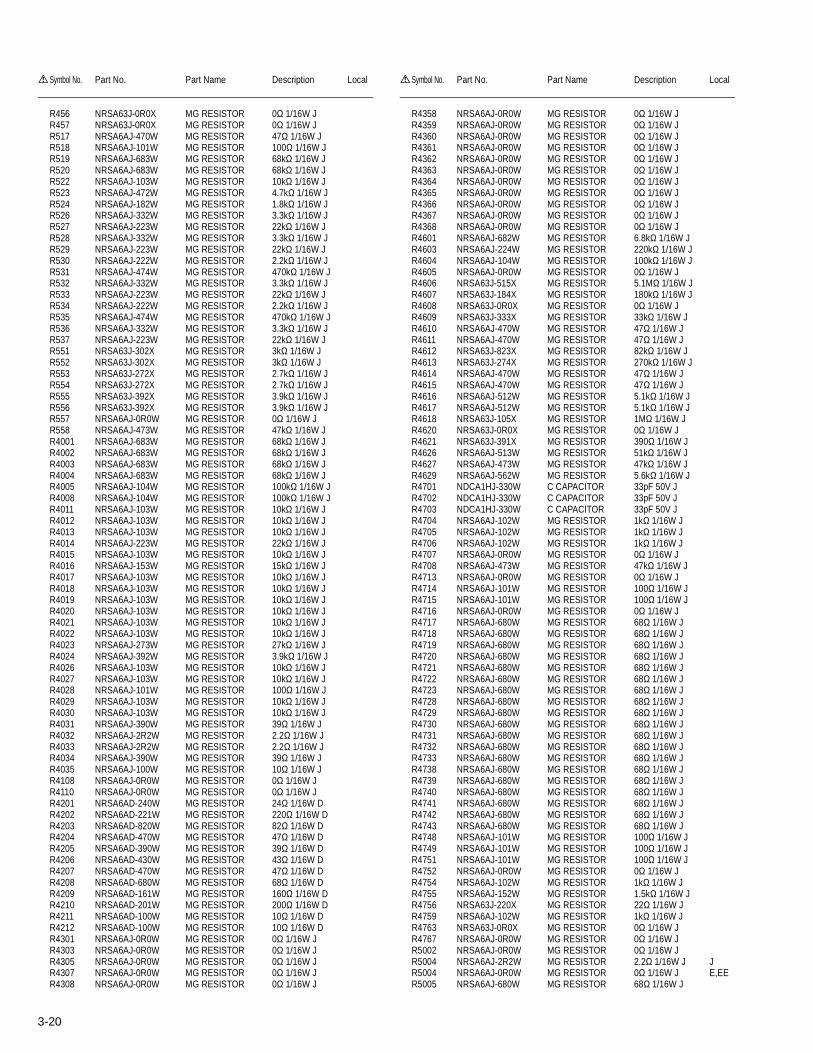
3-20
R456 NRSA63J-0R0X MG RESISTOR 0Ω 1/16W JR457 NRSA63J-0R0X MG RESISTOR 0Ω 1/16W JR517 NRSA6AJ-470W MG RESISTOR 47Ω 1/16W JR518 NRSA6AJ-101W MG RESISTOR 100Ω 1/16W JR519 NRSA6AJ-683W MG RESISTOR 68kΩ 1/16W JR520 NRSA6AJ-683W MG RESISTOR 68kΩ 1/16W JR522 NRSA6AJ-103W MG RESISTOR 10kΩ 1/16W JR523 NRSA6AJ-472W MG RESISTOR 4.7kΩ 1/16W JR524 NRSA6AJ-182W MG RESISTOR 1.8kΩ 1/16W JR526 NRSA6AJ-332W MG RESISTOR 3.3kΩ 1/16W JR527 NRSA6AJ-223W MG RESISTOR 22kΩ 1/16W JR528 NRSA6AJ-332W MG RESISTOR 3.3kΩ 1/16W JR529 NRSA6AJ-223W MG RESISTOR 22kΩ 1/16W JR530 NRSA6AJ-222W MG RESISTOR 2.2kΩ 1/16W JR531 NRSA6AJ-474W MG RESISTOR 470kΩ 1/16W JR532 NRSA6AJ-332W MG RESISTOR 3.3kΩ 1/16W JR533 NRSA6AJ-223W MG RESISTOR 22kΩ 1/16W JR534 NRSA6AJ-222W MG RESISTOR 2.2kΩ 1/16W JR535 NRSA6AJ-474W MG RESISTOR 470kΩ 1/16W JR536 NRSA6AJ-332W MG RESISTOR 3.3kΩ 1/16W JR537 NRSA6AJ-223W MG RESISTOR 22kΩ 1/16W JR551 NRSA63J-302X MG RESISTOR 3kΩ 1/16W JR552 NRSA63J-302X MG RESISTOR 3kΩ 1/16W JR553 NRSA63J-272X MG RESISTOR 2.7kΩ 1/16W JR554 NRSA63J-272X MG RESISTOR 2.7kΩ 1/16W JR555 NRSA63J-392X MG RESISTOR 3.9kΩ 1/16W JR556 NRSA63J-392X MG RESISTOR 3.9kΩ 1/16W JR557 NRSA6AJ-0R0W MG RESISTOR 0Ω 1/16W JR558 NRSA6AJ-473W MG RESISTOR 47kΩ 1/16W JR4001 NRSA6AJ-683W MG RESISTOR 68kΩ 1/16W JR4002 NRSA6AJ-683W MG RESISTOR 68kΩ 1/16W JR4003 NRSA6AJ-683W MG RESISTOR 68kΩ 1/16W JR4004 NRSA6AJ-683W MG RESISTOR 68kΩ 1/16W JR4005 NRSA6AJ-104W MG RESISTOR 100kΩ 1/16W JR4008 NRSA6AJ-104W MG RESISTOR 100kΩ 1/16W JR4011 NRSA6AJ-103W MG RESISTOR 10kΩ 1/16W JR4012 NRSA6AJ-103W MG RESISTOR 10kΩ 1/16W JR4013 NRSA6AJ-103W MG RESISTOR 10kΩ 1/16W JR4014 NRSA6AJ-223W MG RESISTOR 22kΩ 1/16W JR4015 NRSA6AJ-103W MG RESISTOR 10kΩ 1/16W JR4016 NRSA6AJ-153W MG RESISTOR 15kΩ 1/16W JR4017 NRSA6AJ-103W MG RESISTOR 10kΩ 1/16W JR4018 NRSA6AJ-103W MG RESISTOR 10kΩ 1/16W JR4019 NRSA6AJ-103W MG RESISTOR 10kΩ 1/16W JR4020 NRSA6AJ-103W MG RESISTOR 10kΩ 1/16W JR4021 NRSA6AJ-103W MG RESISTOR 10kΩ 1/16W JR4022 NRSA6AJ-103W MG RESISTOR 10kΩ 1/16W JR4023 NRSA6AJ-273W MG RESISTOR 27kΩ 1/16W JR4024 NRSA6AJ-392W MG RESISTOR 3.9kΩ 1/16W JR4026 NRSA6AJ-103W MG RESISTOR 10kΩ 1/16W JR4027 NRSA6AJ-103W MG RESISTOR 10kΩ 1/16W JR4028 NRSA6AJ-101W MG RESISTOR 100Ω 1/16W JR4029 NRSA6AJ-103W MG RESISTOR 10kΩ 1/16W JR4030 NRSA6AJ-103W MG RESISTOR 10kΩ 1/16W JR4031 NRSA6AJ-390W MG RESISTOR 39Ω 1/16W JR4032 NRSA6AJ-2R2W MG RESISTOR 2.2Ω 1/16W JR4033 NRSA6AJ-2R2W MG RESISTOR 2.2Ω 1/16W JR4034 NRSA6AJ-390W MG RESISTOR 39Ω 1/16W JR4035 NRSA6AJ-100W MG RESISTOR 10Ω 1/16W JR4108 NRSA6AJ-0R0W MG RESISTOR 0Ω 1/16W JR4110 NRSA6AJ-0R0W MG RESISTOR 0Ω 1/16W JR4201 NRSA6AD-240W MG RESISTOR 24Ω 1/16W DR4202 NRSA6AD-221W MG RESISTOR 220Ω 1/16W DR4203 NRSA6AD-820W MG RESISTOR 82Ω 1/16W DR4204 NRSA6AD-470W MG RESISTOR 47Ω 1/16W DR4205 NRSA6AD-390W MG RESISTOR 39Ω 1/16W DR4206 NRSA6AD-430W MG RESISTOR 43Ω 1/16W DR4207 NRSA6AD-470W MG RESISTOR 47Ω 1/16W DR4208 NRSA6AD-680W MG RESISTOR 68Ω 1/16W DR4209 NRSA6AD-161W MG RESISTOR 160Ω 1/16W DR4210 NRSA6AD-201W MG RESISTOR 200Ω 1/16W DR4211 NRSA6AD-100W MG RESISTOR 10Ω 1/16W DR4212 NRSA6AD-100W MG RESISTOR 10Ω 1/16W DR4301 NRSA6AJ-0R0W MG RESISTOR 0Ω 1/16W JR4303 NRSA6AJ-0R0W MG RESISTOR 0Ω 1/16W JR4305 NRSA6AJ-0R0W MG RESISTOR 0Ω 1/16W JR4307 NRSA6AJ-0R0W MG RESISTOR 0Ω 1/16W JR4308 NRSA6AJ-0R0W MG RESISTOR 0Ω 1/16W J
Symbol No. Part No. Part Name Description Local
R4358 NRSA6AJ-0R0W MG RESISTOR 0Ω 1/16W JR4359 NRSA6AJ-0R0W MG RESISTOR 0Ω 1/16W JR4360 NRSA6AJ-0R0W MG RESISTOR 0Ω 1/16W JR4361 NRSA6AJ-0R0W MG RESISTOR 0Ω 1/16W JR4362 NRSA6AJ-0R0W MG RESISTOR 0Ω 1/16W JR4363 NRSA6AJ-0R0W MG RESISTOR 0Ω 1/16W JR4364 NRSA6AJ-0R0W MG RESISTOR 0Ω 1/16W JR4365 NRSA6AJ-0R0W MG RESISTOR 0Ω 1/16W JR4366 NRSA6AJ-0R0W MG RESISTOR 0Ω 1/16W JR4367 NRSA6AJ-0R0W MG RESISTOR 0Ω 1/16W JR4368 NRSA6AJ-0R0W MG RESISTOR 0Ω 1/16W JR4601 NRSA6AJ-682W MG RESISTOR 6.8kΩ 1/16W JR4603 NRSA6AJ-224W MG RESISTOR 220kΩ 1/16W JR4604 NRSA6AJ-104W MG RESISTOR 100kΩ 1/16W JR4605 NRSA6AJ-0R0W MG RESISTOR 0Ω 1/16W JR4606 NRSA63J-515X MG RESISTOR 5.1MΩ 1/16W JR4607 NRSA63J-184X MG RESISTOR 180kΩ 1/16W JR4608 NRSA63J-0R0X MG RESISTOR 0Ω 1/16W JR4609 NRSA63J-333X MG RESISTOR 33kΩ 1/16W JR4610 NRSA6AJ-470W MG RESISTOR 47Ω 1/16W JR4611 NRSA6AJ-470W MG RESISTOR 47Ω 1/16W JR4612 NRSA63J-823X MG RESISTOR 82kΩ 1/16W JR4613 NRSA63J-274X MG RESISTOR 270kΩ 1/16W JR4614 NRSA6AJ-470W MG RESISTOR 47Ω 1/16W JR4615 NRSA6AJ-470W MG RESISTOR 47Ω 1/16W JR4616 NRSA6AJ-512W MG RESISTOR 5.1kΩ 1/16W JR4617 NRSA6AJ-512W MG RESISTOR 5.1kΩ 1/16W JR4618 NRSA63J-105X MG RESISTOR 1MΩ 1/16W JR4620 NRSA63J-0R0X MG RESISTOR 0Ω 1/16W JR4621 NRSA63J-391X MG RESISTOR 390Ω 1/16W JR4626 NRSA6AJ-513W MG RESISTOR 51kΩ 1/16W JR4627 NRSA6AJ-473W MG RESISTOR 47kΩ 1/16W JR4629 NRSA6AJ-562W MG RESISTOR 5.6kΩ 1/16W JR4701 NDCA1HJ-330W C CAPACITOR 33pF 50V JR4702 NDCA1HJ-330W C CAPACITOR 33pF 50V JR4703 NDCA1HJ-330W C CAPACITOR 33pF 50V JR4704 NRSA6AJ-102W MG RESISTOR 1kΩ 1/16W JR4705 NRSA6AJ-102W MG RESISTOR 1kΩ 1/16W JR4706 NRSA6AJ-102W MG RESISTOR 1kΩ 1/16W JR4707 NRSA6AJ-0R0W MG RESISTOR 0Ω 1/16W JR4708 NRSA6AJ-473W MG RESISTOR 47kΩ 1/16W JR4713 NRSA6AJ-0R0W MG RESISTOR 0Ω 1/16W JR4714 NRSA6AJ-101W MG RESISTOR 100Ω 1/16W JR4715 NRSA6AJ-101W MG RESISTOR 100Ω 1/16W JR4716 NRSA6AJ-0R0W MG RESISTOR 0Ω 1/16W JR4717 NRSA6AJ-680W MG RESISTOR 68Ω 1/16W JR4718 NRSA6AJ-680W MG RESISTOR 68Ω 1/16W JR4719 NRSA6AJ-680W MG RESISTOR 68Ω 1/16W JR4720 NRSA6AJ-680W MG RESISTOR 68Ω 1/16W JR4721 NRSA6AJ-680W MG RESISTOR 68Ω 1/16W JR4722 NRSA6AJ-680W MG RESISTOR 68Ω 1/16W JR4723 NRSA6AJ-680W MG RESISTOR 68Ω 1/16W JR4728 NRSA6AJ-680W MG RESISTOR 68Ω 1/16W JR4729 NRSA6AJ-680W MG RESISTOR 68Ω 1/16W JR4730 NRSA6AJ-680W MG RESISTOR 68Ω 1/16W JR4731 NRSA6AJ-680W MG RESISTOR 68Ω 1/16W JR4732 NRSA6AJ-680W MG RESISTOR 68Ω 1/16W JR4733 NRSA6AJ-680W MG RESISTOR 68Ω 1/16W JR4738 NRSA6AJ-680W MG RESISTOR 68Ω 1/16W JR4739 NRSA6AJ-680W MG RESISTOR 68Ω 1/16W JR4740 NRSA6AJ-680W MG RESISTOR 68Ω 1/16W JR4741 NRSA6AJ-680W MG RESISTOR 68Ω 1/16W JR4742 NRSA6AJ-680W MG RESISTOR 68Ω 1/16W JR4743 NRSA6AJ-680W MG RESISTOR 68Ω 1/16W JR4748 NRSA6AJ-101W MG RESISTOR 100Ω 1/16W JR4749 NRSA6AJ-101W MG RESISTOR 100Ω 1/16W JR4751 NRSA6AJ-101W MG RESISTOR 100Ω 1/16W JR4752 NRSA6AJ-0R0W MG RESISTOR 0Ω 1/16W JR4754 NRSA6AJ-102W MG RESISTOR 1kΩ 1/16W JR4755 NRSA6AJ-152W MG RESISTOR 1.5kΩ 1/16W JR4756 NRSA63J-220X MG RESISTOR 22Ω 1/16W JR4759 NRSA6AJ-102W MG RESISTOR 1kΩ 1/16W JR4763 NRSA63J-0R0X MG RESISTOR 0Ω 1/16W JR4767 NRSA6AJ-0R0W MG RESISTOR 0Ω 1/16W JR5002 NRSA6AJ-0R0W MG RESISTOR 0Ω 1/16W JR5004 NRSA6AJ-2R2W MG RESISTOR 2.2Ω 1/16W J JR5004 NRSA6AJ-0R0W MG RESISTOR 0Ω 1/16W J E,EER5005 NRSA6AJ-680W MG RESISTOR 68Ω 1/16W J
Symbol No. Part No. Part Name Description Local

3-21
Front end boardBlock No. [0][5]
R5006 NRSA6AJ-680W MG RESISTOR 68Ω 1/16W JR5007 NRSA63J-680X MG RESISTOR 68Ω 1/16W JR5008 NRSA63J-0R0X MG RESISTOR 0Ω 1/16W JR5009 NRSA6AJ-330W MG RESISTOR 33Ω 1/16W JR5010 NRSA6AJ-103W MG RESISTOR 10kΩ 1/16W JR5011 NRSA6AJ-103W MG RESISTOR 10kΩ 1/16W JR5013 NRSA6AJ-101W MG RESISTOR 100Ω 1/16W JR5014 NRSA6AJ-101W MG RESISTOR 100Ω 1/16W JR5015 NRSA6AJ-101W MG RESISTOR 100Ω 1/16W JR5016 NRSA6AJ-101W MG RESISTOR 100Ω 1/16W JR5017 NRSA6AJ-101W MG RESISTOR 100Ω 1/16W JR5018 NRSA6AJ-101W MG RESISTOR 100Ω 1/16W JR5019 NRSA6AJ-101W MG RESISTOR 100Ω 1/16W JR5020 NRSA6AJ-101W MG RESISTOR 100Ω 1/16W JR5021 NRSA6AJ-101W MG RESISTOR 100Ω 1/16W JR5022 NRSA6AJ-330W MG RESISTOR 33Ω 1/16W JR5023 NRSA6AJ-101W MG RESISTOR 100Ω 1/16W JR5024 NRSA6AJ-101W MG RESISTOR 100Ω 1/16W JR5025 NRSA6AJ-101W MG RESISTOR 100Ω 1/16W JR5026 NRSA6AJ-101W MG RESISTOR 100Ω 1/16W JR5027 NRSA6AJ-101W MG RESISTOR 100Ω 1/16W JR5028 NRSA6AJ-223W MG RESISTOR 22kΩ 1/16W JR5029 NRSA6AJ-101W MG RESISTOR 100Ω 1/16W JR5030 NRSA6AJ-0R0W MG RESISTOR 0Ω 1/16W JR5031 NRSA6AJ-102W MG RESISTOR 1kΩ 1/16W JR5032 NRSA6AJ-220W MG RESISTOR 22Ω 1/16W JR5034 NRSA6AJ-0R0W MG RESISTOR 0Ω 1/16W JR5036 NRSA6AJ-103W MG RESISTOR 10kΩ 1/16W JR5037 NRSA6AJ-0R0W MG RESISTOR 0Ω 1/16W JR5038 NRSA6AJ-0R0W MG RESISTOR 0Ω 1/16W JR5043 NRSA6AJ-0R0W MG RESISTOR 0Ω 1/16W JR5044 NRSA6AJ-0R0W MG RESISTOR 0Ω 1/16W JR5048 NRSA6AJ-0R0W MG RESISTOR 0Ω 1/16W JR5049 NRSA6AJ-0R0W MG RESISTOR 0Ω 1/16W JR5050 NRSA6AJ-0R0W MG RESISTOR 0Ω 1/16W JR5057 NRSA6AD-123W MG RESISTOR 12kΩ 1/16W DR5058 NRSA6AJ-0R0W MG RESISTOR 0Ω 1/16W JR5059 NRSA6AJ-752W MG RESISTOR 7.5kΩ 1/16W JR5060 NRSA6AJ-622W MG RESISTOR 6.2kΩ 1/16W JR5061 NRSA6AJ-272W MG RESISTOR 2.7kΩ 1/16W JR5062 NRSA6AJ-471W MG RESISTOR 470Ω 1/16W JR5063 NRSA6AJ-471W MG RESISTOR 470Ω 1/16W JR5064 NRSA6AJ-0R0W MG RESISTOR 0Ω 1/16W JR5065 NRSA6AJ-0R0W MG RESISTOR 0Ω 1/16W JR5066 NRSA6AJ-103W MG RESISTOR 10kΩ 1/16W JR5068 NRSA6AJ-681W MG RESISTOR 680Ω 1/16W JR5069 NRSA6AJ-0R0W MG RESISTOR 0Ω 1/16W JR5070 NRSA6AJ-0R0W MG RESISTOR 0Ω 1/16W JR5071 NRSA6AJ-0R0W MG RESISTOR 0Ω 1/16W JR5072 NRSA6AJ-103W MG RESISTOR 10kΩ 1/16W JR5074 NRSA6AJ-0R0W MG RESISTOR 0Ω 1/16W JR5076 NRSA6AJ-0R0W MG RESISTOR 0Ω 1/16W JR5077 NRSA6AJ-0R0W MG RESISTOR 0Ω 1/16W JR5078 NRSA6AJ-103W MG RESISTOR 10kΩ 1/16W JR5079 NRSA6AJ-0R0W MG RESISTOR 0Ω 1/16W JR5080 NRSA6AJ-0R0W MG RESISTOR 0Ω 1/16W JR5081 NRSA6AJ-0R0W MG RESISTOR 0Ω 1/16W JR5082 NRSA6AJ-0R0W MG RESISTOR 0Ω 1/16W JR5083 NRSA6AJ-0R0W MG RESISTOR 0Ω 1/16W JR5084 NRSA6AJ-0R0W MG RESISTOR 0Ω 1/16W JR5085 NRSA6AJ-220W MG RESISTOR 22Ω 1/16W JR5086 NRSA6AJ-101W MG RESISTOR 100Ω 1/16W JR5087 NRSA6AJ-330W MG RESISTOR 33Ω 1/16W JR5092 NRSA6AJ-330W MG RESISTOR 33Ω 1/16W JR5097 NRSA6AJ-330W MG RESISTOR 33Ω 1/16W JR5098 NRSA6AJ-330W MG RESISTOR 33Ω 1/16W JR5099 NRSA6AJ-330W MG RESISTOR 33Ω 1/16W JR5100 NRSA6AJ-330W MG RESISTOR 33Ω 1/16W JR5101 NRSA6AJ-221W MG RESISTOR 220Ω 1/16W JR5102 NRSA6AJ-221W MG RESISTOR 220Ω 1/16W JR5103 NRSA6AJ-471W MG RESISTOR 470Ω 1/16W JR5105 NRSA6AJ-391W MG RESISTOR 390Ω 1/16W JR5106 NRSA63J-152X MG RESISTOR 1.5kΩ 1/16W JR5113 NRSA63J-103X MG RESISTOR 10kΩ 1/16W JR5114 NRSA63J-103X MG RESISTOR 10kΩ 1/16W JR5115 NRSA6AJ-101W MG RESISTOR 100Ω 1/16W JR5201 NRSA6AJ-102W MG RESISTOR 1kΩ 1/16W JR5202 NRSA6AJ-102W MG RESISTOR 1kΩ 1/16W J
Symbol No. Part No. Part Name Description Local
R5204 NRSA6AJ-0R0W MG RESISTOR 0Ω 1/16W JR5206 NRSA6AJ-0R0W MG RESISTOR 0Ω 1/16W JR5207 NRSA6AJ-0R0W MG RESISTOR 0Ω 1/16W JR5208 NRSA6AJ-0R0W MG RESISTOR 0Ω 1/16W JR5209 NRSA6AJ-0R0W MG RESISTOR 0Ω 1/16W JR5210 NRSA6AJ-0R0W MG RESISTOR 0Ω 1/16W JR5211 NRSA6AJ-0R0W MG RESISTOR 0Ω 1/16W JR5302 NRSA63J-103X MG RESISTOR 10kΩ 1/16W JRA501 NRZ0034-680W NET RESISTOR 68Ω 1/32W J x4RA502 NRZ0034-680W NET RESISTOR 68Ω 1/32W J x4RA503 NRZ0034-680W NET RESISTOR 68Ω 1/32W J x4RA504 NRZ0034-680W NET RESISTOR 68Ω 1/32W J x4RA505 NRZ0034-680W NET RESISTOR 68Ω 1/32W J x4RA506 NRZ0034-680W NET RESISTOR 68Ω 1/32W J x4RA507 NRZ0034-680W NET RESISTOR 68Ω 1/32W J x4RA508 NRZ0034-680W NET RESISTOR 68Ω 1/32W J x4RA509 NRZ0034-680W NET RESISTOR 68Ω 1/32W J x4RA520 NRZ0034-330W NET RESISTOR 33Ω 1/32W J x4RA521 NRZ0034-330W NET RESISTOR 33Ω 1/32W J x4RA522 NRZ0034-330W NET RESISTOR 33Ω 1/32W J x4
L401 NQL382M-100X COIL 10uH ML4001 NQL79GM-220X COIL 22uH ML4002 NQL79GM-220X COIL 22uH ML4301 NQL382M-470X COIL 47uH ML4302 NQL382M-470X COIL 47uH ML4601 NQL382M-470X COIL 47uH ML4602 NQL52EM-100X COIL 10uH ML4702 NQL382M-220X COIL 22uH ML5001 NQL382M-220X COIL 22uH ML5004 NQL382M-220X COIL 22uH ML5005 NQL085J-470X COIL 47uH JT4601 NQR0636-001 C FL TRANSF
CN401 QGF0534F2-60X CONNECTOR FFC/FPC (1-60)CN403 QGA8002F1-02X CONNECTOR W-B (1-2)CN404 QGF0522F3-09W CONNECTOR FFC/FPC (1-9)CN501 QGF0523F2-16W CONNECTOR FFC/FPC (1-16)CN502 QGF1039F2-04X CONNECTOR FFC/FPC (1-4)CN503 QGF0534F3-60X CONNECTOR FFC/FPC (1-60)CN504 QGF0522F3-15W CONNECTOR FFC/FPC (1-15)CN551 QGF0545F3-16X CONNECTOR FFC/FPC (1-16)K501 NRSA63J-0R0X MG RESISTOR 0Ω 1/16W JK502 NRSA63J-0R0X MG RESISTOR 0Ω 1/16W JK503 NRSA63J-0R0X MG RESISTOR 0Ω 1/16W JK504 NRSA63J-0R0X MG RESISTOR 0Ω 1/16W JS551 NSW0312-001X TACT SWITCHS552 NSW0312-001X TACT SWITCHS553 NSW0312-001X TACT SWITCHS554 NSW0312-001X TACT SWITCHS555 NSW0312-001X TACT SWITCHS556 NSW0312-001X TACT SWITCHS557 NSW0312-001X TACT SWITCHS558 NSW0312-001X TACT SWITCHS559 NSW0312-001X TACT SWITCHX401 NAX0974-001X CRYSTALX5001 NAX0971-001X CRYSTALX5002 NAX0970-001X CRYSTAL
Symbol No. Part No. Part Name Description Local
IC1 BD8215EFV-X ICIC3 MM3233DF-X ICIC7 TC7PA53FU-X ICIC301 MN2DS0018MA ICIC302 MM1701CH-X ICIC307 MFI341S2094-X IC(MCU)IC308 NJU6368PF1-X ICIC398 SG32A90TFIR36V IC(PROGRAMED)IC399 M12L128168A-7TG IC(DIGITAL)IC399 or K4S281632I-UC75 IC(DIGITAL)
Symbol No. Part No. Part Name Description Local

3-22
IC400 AK4387ET-X ICIC481 BR24L32FV-W-X IC(DIGITAL)IC501 TC74LCX373FT-X IC(DIGITAL)IC502 TC74LCX373FT-X IC(DIGITAL)
Q2 RT1N141U-X RANSISTORQ4 2SC3928A/R/-X TRANSISTORQ4 or 2SD601A/R/-X TRANSISTORQ7 2SC3928A/R/-X TRANSISTORQ7 or 2SD601A/R/-X TRANSISTORQ8 2SA1774/R/-X TRANSISTORQ9 2SC4617/R/-X TRANSISTORQ101 2SB1424/R/-W TRANSISTORQ102 2SC4617/R/-X TRANSISTORQ103 2SB1424/R/-W TRANSISTORQ104 2SC4617/R/-X TRANSISTORQ105 2SC4617/R/-X TRANSISTORQ106 2SK3546J-X MOS FETQ107 2SK3546J-X MOS FETQ301 RT1N441U-X TRANSISTORQ302 RT1N441U-X TRANSISTOR
D6 AN1102W-6-X IR LEDD7 AN1102W-6-X IR LEDD9 PS1192HB-22-X PHOTO
TRANSISTORD11 PS1192HB-22-X PHOTO
TRANSISTOR
C2 NCB31CK-104X C CAPACITOR 0.1uF 16V KC3 NCB31CK-104X C CAPACITOR 0.1uF 16V KC4 NCB31CK-104X C CAPACITOR 0.1uF 16V KC5 NCB31CK-104X C CAPACITOR 0.1uF 16V KC6 NCB31CK-104X C CAPACITOR 0.1uF 16V KC7 NCB31CK-104X C CAPACITOR 0.1uF 16V KC8 NCB31CK-104X C CAPACITOR 0.1uF 16V KC9 NCB31CK-104X C CAPACITOR 0.1uF 16V KC11 NCB31CK-104X C CAPACITOR 0.1uF 16V KC12 NCB31CK-104X C CAPACITOR 0.1uF 16V KC13 NCB31CK-104X C CAPACITOR 0.1uF 16V KC14 NCB31CK-104X C CAPACITOR 0.1uF 16V KC15 NCB31CK-104X C CAPACITOR 0.1uF 16V KC16 NCB31CK-104X C CAPACITOR 0.1uF 16V KC17 NCB31CK-104X C CAPACITOR 0.1uF 16V KC18 NCB31CK-104X C CAPACITOR 0.1uF 16V KC19 NCB31CK-104X C CAPACITOR 0.1uF 16V KC20 NCB31CK-104X C CAPACITOR 0.1uF 16V KC21 NBE41AM-476X TA E CAPACITOR 47uF 10V MC22 NBE41AM-476X TA E CAPACITOR 47uF 10V MC23 NBE41AM-476X TA E CAPACITOR 47uF 10V MC24 NCB31CK-104X C CAPACITOR 0.1uF 16V KC25 NCB31CK-104X C CAPACITOR 0.1uF 16V KC26 NCB31CK-104X C CAPACITOR 0.1uF 16V KC31 NCB31HK-681X C CAPACITOR 680pF 50V KC32 NCB31HK-561X C CAPACITOR 560pF 50V KC48 NCB31CK-104X C CAPACITOR 0.1uF 16V KC50 NCB31CK-104X C CAPACITOR 0.1uF 16V KC51 NDC31HJ-4R0X C CAPACITOR 4pF 50V JC52 NDC31HJ-4R0X C CAPACITOR 4pF 50V JC60 NCB31HK-103X C CAPACITOR 0.01uF 50V KC63 NBE40JM-476X TA E CAPACITOR 47uF 6.3V MC65 NCB31CK-104X C CAPACITOR 0.1uF 16V KC66 NCB31CK-104X C CAPACITOR 0.1uF 16V KC67 NCB31HK-103X C CAPACITOR 0.01uF 50V KC68 NCB31CK-104X C CAPACITOR 0.1uF 16V KC69 NCB21CK-105X C CAPACITOR 1uF 16V KC70 NCB31CK-104X C CAPACITOR 0.1uF 16V KC71 NCB31CK-104X C CAPACITOR 0.1uF 16V KC72 NCB31CK-105X C CAPACITOR 1uF 16V KC73 NCB31CK-104X C CAPACITOR 0.1uF 16V KC74 NCB31CK-104X C CAPACITOR 0.1uF 16V KC75 NCB31CK-104X C CAPACITOR 0.1uF 16V KC76 NCB31CK-104X C CAPACITOR 0.1uF 16V KC77 NCB31CK-104X C CAPACITOR 0.1uF 16V KC78 NCB31CK-104X C CAPACITOR 0.1uF 16V KC79 NCB31CK-104X C CAPACITOR 0.1uF 16V KC80 NCB21CK-105X C CAPACITOR 1uF 16V KC81 NDC31HJ-120X C CAPACITOR 12pF 50V J
Symbol No. Part No. Part Name Description Local
C82 NDC31HJ-150X C CAPACITOR 15pF 50V JC83 NCB31CK-104X C CAPACITOR 0.1uF 16V KC84 NCB31CK-333X C CAPACITOR 0.033uF 16V KC85 NCB31CK-104X C CAPACITOR 0.1uF 16V KC86 NCB31CK-104X C CAPACITOR 0.1uF 16V KC87 NCB31CK-104X C CAPACITOR 0.1uF 16V KC88 NCB31CK-104X C CAPACITOR 0.1uF 16V KC89 NCB31HK-183X C CAPACITOR 0.018uF 50V KC90 NCB31HK-562X C CAPACITOR 5600pF 50V KC91 NCB31CK-104X C CAPACITOR 0.1uF 16V KC92 NCB21CK-105X C CAPACITOR 1uF 16V KC93 NCB21CK-105X C CAPACITOR 1uF 16V KC99 NCB31CK-104X C CAPACITOR 0.1uF 16V KC100 NCB31CK-684X C CAPACITOR 0.68uF 16V KC101 NCB31CK-104X C CAPACITOR 0.1uF 16V KC102 NCB31CK-684X C CAPACITOR 0.68uF 16V KC109 NCB21CK-105X C CAPACITOR 1uF 16V KC113 NCB21CK-105X C CAPACITOR 1uF 16V KC117 NCB21CK-105X C CAPACITOR 1uF 16V KC118 NCB31HK-103X C CAPACITOR 0.01uF 50V KC121 NCB31CK-104X C CAPACITOR 0.1uF 16V KC122 NCB31CK-104X C CAPACITOR 0.1uF 16V KC126 NCB31CK-104X C CAPACITOR 0.1uF 16V KC127 NCB31CK-104X C CAPACITOR 0.1uF 16V KC128 NCB31CK-104X C CAPACITOR 0.1uF 16V KC129 NCB31CK-104X C CAPACITOR 0.1uF 16V KC130 NCB31CK-104X C CAPACITOR 0.1uF 16V KC131 NCB31CK-104X C CAPACITOR 0.1uF 16V KC132 NCB31CK-104X C CAPACITOR 0.1uF 16V KC133 NCB31CK-104X C CAPACITOR 0.1uF 16V KC134 NCB31CK-104X C CAPACITOR 0.1uF 16V KC135 NCB31CK-104X C CAPACITOR 0.1uF 16V KC136 NCB31CK-104X C CAPACITOR 0.1uF 16V KC137 NBE20JM-226X TA E CAPACITOR 22uF 6.3V MC139 NBE20JM-226X TA E CAPACITOR 22uF 6.3V MC142 NCB31CK-104X C CAPACITOR 0.1uF 16V KC143 NBE41AM-476X TA E CAPACITOR 47uF 10V MC145 NBE41AM-476X TA E CAPACITOR 47uF 10V MC147 NCB31CK-104X C CAPACITOR 0.1uF 16V KC148 NCB31HK-331X C CAPACITOR 330pF 50V KC149 NCB31CK-104X C CAPACITOR 0.1uF 16V KC151 NCB31CK-473X C CAPACITOR 0.047uF 16V KC155 NDC31HJ-101X C CAPACITOR 100pF 50V JC156 NCB31CK-104X C CAPACITOR 0.1uF 16V KC161 NCB31CK-104X C CAPACITOR 0.1uF 16V KC162 NCB31CK-104X C CAPACITOR 0.1uF 16V KC164 NCB21CK-105X C CAPACITOR 1uF 16V KC165 NCB31CK-104X C CAPACITOR 0.1uF 16V KC167 NDC31HJ-272X C CAPACITOR 2700pF 50V JC170 NCB31CK-104X C CAPACITOR 0.1uF 16V KC173 NCB31CK-104X C CAPACITOR 0.1uF 16V KC174 NCB31CK-104X C CAPACITOR 0.1uF 16V KC175 NBE61CM-107X TA E CAPACITOR 100uF 16V MC176 NCB31CK-104X C CAPACITOR 0.1uF 16V KC177 NCB31CK-104X C CAPACITOR 0.1uF 16V KC178 NCB31CK-104X C CAPACITOR 0.1uF 16V KC197 NCB31CK-104X C CAPACITOR 0.1uF 16V KC199 NCB31CK-104X C CAPACITOR 0.1uF 16V KC200 NBE40JM-476X TA E CAPACITOR 47uF 6.3V MC201 NCB31CK-104X C CAPACITOR 0.1uF 16V KC205 NCB21AK-225X C CAPACITOR 2.2uF 10V KC206 NDC31HJ-222X C CAPACITOR 2200pF 50V JC211 NCB31CK-104X C CAPACITOR 0.1uF 16V KC215 NDC31HJ-181X C CAPACITOR 180pF 50V JC216 NCB31CK-104X C CAPACITOR 0.1uF 16V KC218 NCB31CK-104X C CAPACITOR 0.1uF 16V KC219 NCB31CK-223X C CAPACITOR 0.022uF 16V KC220 NCB31HK-102X C CAPACITOR 1000pF 50V KC222 NCB31CK-104X C CAPACITOR 0.1uF 16V KC223 NCB31HK-102X C CAPACITOR 1000pF 50V KC224 NCB21AK-225X C CAPACITOR 2.2uF 10V KC225 NBE61CM-107X TA E CAPACITOR 100uF 16V MC228 NCB31HK-102X C CAPACITOR 1000pF 50V KC229 NCB31CK-223X C CAPACITOR 0.022uF 16V KC232 NBE61CM-107X TA E CAPACITOR 100uF 16V MC233 NCB21CK-105X C CAPACITOR 1uF 16V KC235 NCB31HK-102X C CAPACITOR 1000pF 50V KC237 NDC31HJ-221X C CAPACITOR 220pF 50V J
Symbol No. Part No. Part Name Description Local
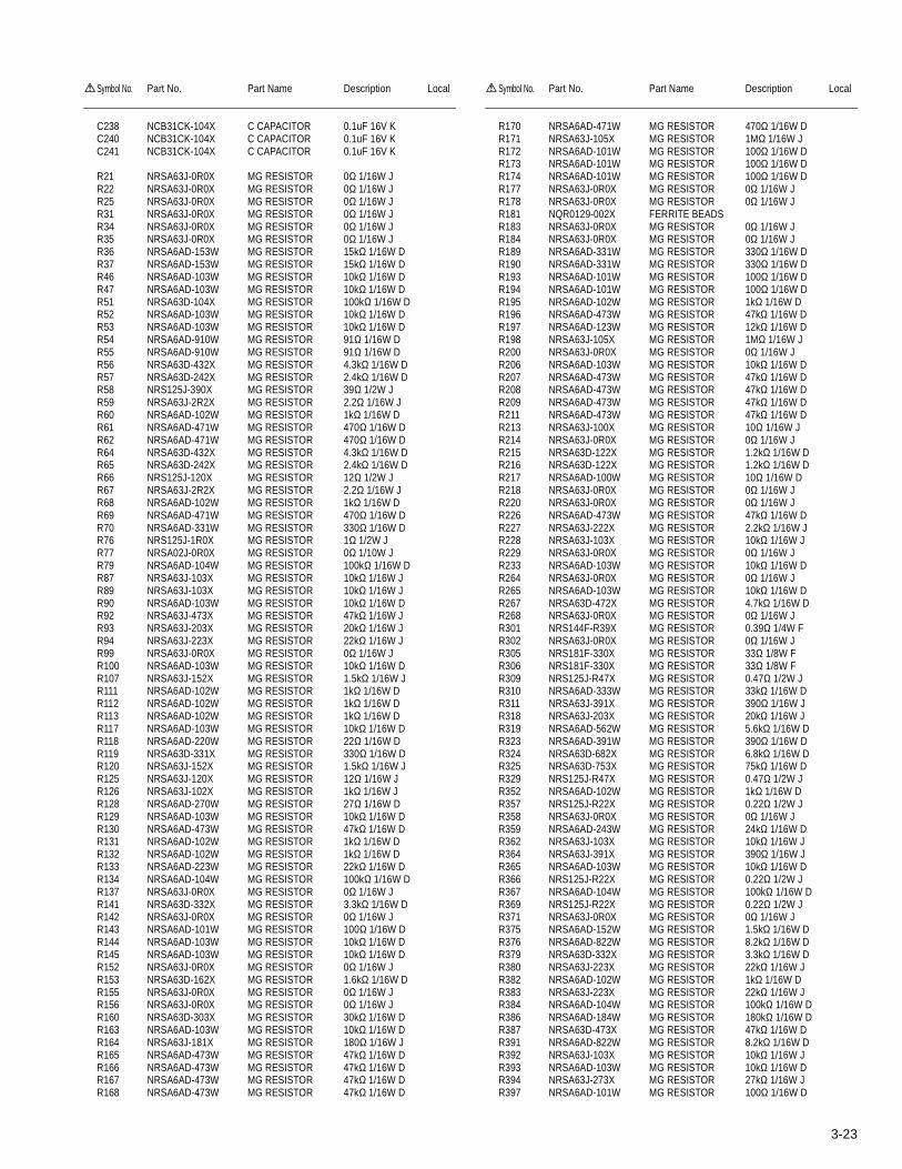
3-23
C238 NCB31CK-104X C CAPACITOR 0.1uF 16V KC240 NCB31CK-104X C CAPACITOR 0.1uF 16V KC241 NCB31CK-104X C CAPACITOR 0.1uF 16V K
R21 NRSA63J-0R0X MG RESISTOR 0Ω 1/16W JR22 NRSA63J-0R0X MG RESISTOR 0Ω 1/16W JR25 NRSA63J-0R0X MG RESISTOR 0Ω 1/16W JR31 NRSA63J-0R0X MG RESISTOR 0Ω 1/16W JR34 NRSA63J-0R0X MG RESISTOR 0Ω 1/16W JR35 NRSA63J-0R0X MG RESISTOR 0Ω 1/16W JR36 NRSA6AD-153W MG RESISTOR 15kΩ 1/16W DR37 NRSA6AD-153W MG RESISTOR 15kΩ 1/16W DR46 NRSA6AD-103W MG RESISTOR 10kΩ 1/16W DR47 NRSA6AD-103W MG RESISTOR 10kΩ 1/16W DR51 NRSA63D-104X MG RESISTOR 100kΩ 1/16W DR52 NRSA6AD-103W MG RESISTOR 10kΩ 1/16W DR53 NRSA6AD-103W MG RESISTOR 10kΩ 1/16W DR54 NRSA6AD-910W MG RESISTOR 91Ω 1/16W DR55 NRSA6AD-910W MG RESISTOR 91Ω 1/16W DR56 NRSA63D-432X MG RESISTOR 4.3kΩ 1/16W DR57 NRSA63D-242X MG RESISTOR 2.4kΩ 1/16W DR58 NRS125J-390X MG RESISTOR 39Ω 1/2W JR59 NRSA63J-2R2X MG RESISTOR 2.2Ω 1/16W JR60 NRSA6AD-102W MG RESISTOR 1kΩ 1/16W DR61 NRSA6AD-471W MG RESISTOR 470Ω 1/16W DR62 NRSA6AD-471W MG RESISTOR 470Ω 1/16W DR64 NRSA63D-432X MG RESISTOR 4.3kΩ 1/16W DR65 NRSA63D-242X MG RESISTOR 2.4kΩ 1/16W DR66 NRS125J-120X MG RESISTOR 12Ω 1/2W JR67 NRSA63J-2R2X MG RESISTOR 2.2Ω 1/16W JR68 NRSA6AD-102W MG RESISTOR 1kΩ 1/16W DR69 NRSA6AD-471W MG RESISTOR 470Ω 1/16W DR70 NRSA6AD-331W MG RESISTOR 330Ω 1/16W DR76 NRS125J-1R0X MG RESISTOR 1Ω 1/2W JR77 NRSA02J-0R0X MG RESISTOR 0Ω 1/10W JR79 NRSA6AD-104W MG RESISTOR 100kΩ 1/16W DR87 NRSA63J-103X MG RESISTOR 10kΩ 1/16W JR89 NRSA63J-103X MG RESISTOR 10kΩ 1/16W JR90 NRSA6AD-103W MG RESISTOR 10kΩ 1/16W DR92 NRSA63J-473X MG RESISTOR 47kΩ 1/16W JR93 NRSA63J-203X MG RESISTOR 20kΩ 1/16W JR94 NRSA63J-223X MG RESISTOR 22kΩ 1/16W JR99 NRSA63J-0R0X MG RESISTOR 0Ω 1/16W JR100 NRSA6AD-103W MG RESISTOR 10kΩ 1/16W DR107 NRSA63J-152X MG RESISTOR 1.5kΩ 1/16W JR111 NRSA6AD-102W MG RESISTOR 1kΩ 1/16W DR112 NRSA6AD-102W MG RESISTOR 1kΩ 1/16W DR113 NRSA6AD-102W MG RESISTOR 1kΩ 1/16W DR117 NRSA6AD-103W MG RESISTOR 10kΩ 1/16W DR118 NRSA6AD-220W MG RESISTOR 22Ω 1/16W DR119 NRSA63D-331X MG RESISTOR 330Ω 1/16W DR120 NRSA63J-152X MG RESISTOR 1.5kΩ 1/16W JR125 NRSA63J-120X MG RESISTOR 12Ω 1/16W JR126 NRSA63J-102X MG RESISTOR 1kΩ 1/16W JR128 NRSA6AD-270W MG RESISTOR 27Ω 1/16W DR129 NRSA6AD-103W MG RESISTOR 10kΩ 1/16W DR130 NRSA6AD-473W MG RESISTOR 47kΩ 1/16W DR131 NRSA6AD-102W MG RESISTOR 1kΩ 1/16W DR132 NRSA6AD-102W MG RESISTOR 1kΩ 1/16W DR133 NRSA6AD-223W MG RESISTOR 22kΩ 1/16W DR134 NRSA6AD-104W MG RESISTOR 100kΩ 1/16W DR137 NRSA63J-0R0X MG RESISTOR 0Ω 1/16W JR141 NRSA63D-332X MG RESISTOR 3.3kΩ 1/16W DR142 NRSA63J-0R0X MG RESISTOR 0Ω 1/16W JR143 NRSA6AD-101W MG RESISTOR 100Ω 1/16W DR144 NRSA6AD-103W MG RESISTOR 10kΩ 1/16W DR145 NRSA6AD-103W MG RESISTOR 10kΩ 1/16W DR152 NRSA63J-0R0X MG RESISTOR 0Ω 1/16W JR153 NRSA63D-162X MG RESISTOR 1.6kΩ 1/16W DR155 NRSA63J-0R0X MG RESISTOR 0Ω 1/16W JR156 NRSA63J-0R0X MG RESISTOR 0Ω 1/16W JR160 NRSA63D-303X MG RESISTOR 30kΩ 1/16W DR163 NRSA6AD-103W MG RESISTOR 10kΩ 1/16W DR164 NRSA63J-181X MG RESISTOR 180Ω 1/16W JR165 NRSA6AD-473W MG RESISTOR 47kΩ 1/16W DR166 NRSA6AD-473W MG RESISTOR 47kΩ 1/16W DR167 NRSA6AD-473W MG RESISTOR 47kΩ 1/16W DR168 NRSA6AD-473W MG RESISTOR 47kΩ 1/16W D
Symbol No. Part No. Part Name Description Local
R170 NRSA6AD-471W MG RESISTOR 470Ω 1/16W DR171 NRSA63J-105X MG RESISTOR 1MΩ 1/16W JR172 NRSA6AD-101W MG RESISTOR 100Ω 1/16W DR173 NRSA6AD-101W MG RESISTOR 100Ω 1/16W DR174 NRSA6AD-101W MG RESISTOR 100Ω 1/16W DR177 NRSA63J-0R0X MG RESISTOR 0Ω 1/16W JR178 NRSA63J-0R0X MG RESISTOR 0Ω 1/16W JR181 NQR0129-002X FERRITE BEADSR183 NRSA63J-0R0X MG RESISTOR 0Ω 1/16W JR184 NRSA63J-0R0X MG RESISTOR 0Ω 1/16W JR189 NRSA6AD-331W MG RESISTOR 330Ω 1/16W DR190 NRSA6AD-331W MG RESISTOR 330Ω 1/16W DR193 NRSA6AD-101W MG RESISTOR 100Ω 1/16W DR194 NRSA6AD-101W MG RESISTOR 100Ω 1/16W DR195 NRSA6AD-102W MG RESISTOR 1kΩ 1/16W DR196 NRSA6AD-473W MG RESISTOR 47kΩ 1/16W DR197 NRSA6AD-123W MG RESISTOR 12kΩ 1/16W DR198 NRSA63J-105X MG RESISTOR 1MΩ 1/16W JR200 NRSA63J-0R0X MG RESISTOR 0Ω 1/16W JR206 NRSA6AD-103W MG RESISTOR 10kΩ 1/16W DR207 NRSA6AD-473W MG RESISTOR 47kΩ 1/16W DR208 NRSA6AD-473W MG RESISTOR 47kΩ 1/16W DR209 NRSA6AD-473W MG RESISTOR 47kΩ 1/16W DR211 NRSA6AD-473W MG RESISTOR 47kΩ 1/16W DR213 NRSA63J-100X MG RESISTOR 10Ω 1/16W JR214 NRSA63J-0R0X MG RESISTOR 0Ω 1/16W JR215 NRSA63D-122X MG RESISTOR 1.2kΩ 1/16W DR216 NRSA63D-122X MG RESISTOR 1.2kΩ 1/16W DR217 NRSA6AD-100W MG RESISTOR 10Ω 1/16W DR218 NRSA63J-0R0X MG RESISTOR 0Ω 1/16W JR220 NRSA63J-0R0X MG RESISTOR 0Ω 1/16W JR226 NRSA6AD-473W MG RESISTOR 47kΩ 1/16W DR227 NRSA63J-222X MG RESISTOR 2.2kΩ 1/16W JR228 NRSA63J-103X MG RESISTOR 10kΩ 1/16W JR229 NRSA63J-0R0X MG RESISTOR 0Ω 1/16W JR233 NRSA6AD-103W MG RESISTOR 10kΩ 1/16W DR264 NRSA63J-0R0X MG RESISTOR 0Ω 1/16W JR265 NRSA6AD-103W MG RESISTOR 10kΩ 1/16W DR267 NRSA63D-472X MG RESISTOR 4.7kΩ 1/16W DR268 NRSA63J-0R0X MG RESISTOR 0Ω 1/16W JR301 NRS144F-R39X MG RESISTOR 0.39Ω 1/4W FR302 NRSA63J-0R0X MG RESISTOR 0Ω 1/16W JR305 NRS181F-330X MG RESISTOR 33Ω 1/8W FR306 NRS181F-330X MG RESISTOR 33Ω 1/8W FR309 NRS125J-R47X MG RESISTOR 0.47Ω 1/2W JR310 NRSA6AD-333W MG RESISTOR 33kΩ 1/16W DR311 NRSA63J-391X MG RESISTOR 390Ω 1/16W JR318 NRSA63J-203X MG RESISTOR 20kΩ 1/16W JR319 NRSA6AD-562W MG RESISTOR 5.6kΩ 1/16W DR323 NRSA6AD-391W MG RESISTOR 390Ω 1/16W DR324 NRSA63D-682X MG RESISTOR 6.8kΩ 1/16W DR325 NRSA63D-753X MG RESISTOR 75kΩ 1/16W DR329 NRS125J-R47X MG RESISTOR 0.47Ω 1/2W JR352 NRSA6AD-102W MG RESISTOR 1kΩ 1/16W DR357 NRS125J-R22X MG RESISTOR 0.22Ω 1/2W JR358 NRSA63J-0R0X MG RESISTOR 0Ω 1/16W JR359 NRSA6AD-243W MG RESISTOR 24kΩ 1/16W DR362 NRSA63J-103X MG RESISTOR 10kΩ 1/16W JR364 NRSA63J-391X MG RESISTOR 390Ω 1/16W JR365 NRSA6AD-103W MG RESISTOR 10kΩ 1/16W DR366 NRS125J-R22X MG RESISTOR 0.22Ω 1/2W JR367 NRSA6AD-104W MG RESISTOR 100kΩ 1/16W DR369 NRS125J-R22X MG RESISTOR 0.22Ω 1/2W JR371 NRSA63J-0R0X MG RESISTOR 0Ω 1/16W JR375 NRSA6AD-152W MG RESISTOR 1.5kΩ 1/16W DR376 NRSA6AD-822W MG RESISTOR 8.2kΩ 1/16W DR379 NRSA63D-332X MG RESISTOR 3.3kΩ 1/16W DR380 NRSA63J-223X MG RESISTOR 22kΩ 1/16W JR382 NRSA6AD-102W MG RESISTOR 1kΩ 1/16W DR383 NRSA63J-223X MG RESISTOR 22kΩ 1/16W JR384 NRSA6AD-104W MG RESISTOR 100kΩ 1/16W DR386 NRSA6AD-184W MG RESISTOR 180kΩ 1/16W DR387 NRSA63D-473X MG RESISTOR 47kΩ 1/16W DR391 NRSA6AD-822W MG RESISTOR 8.2kΩ 1/16W DR392 NRSA63J-103X MG RESISTOR 10kΩ 1/16W JR393 NRSA6AD-103W MG RESISTOR 10kΩ 1/16W DR394 NRSA63J-273X MG RESISTOR 27kΩ 1/16W JR397 NRSA6AD-101W MG RESISTOR 100Ω 1/16W D
Symbol No. Part No. Part Name Description Local

3-24
R400 NRSA6AD-153W MG RESISTOR 15kΩ 1/16W DR402 NRSA6AD-473W MG RESISTOR 47kΩ 1/16W DR403 NRSA63J-101X MG RESISTOR 100Ω 1/16W JR406 NRS125J-R22X MG RESISTOR 0.22Ω 1/2W JR417 NRSA63J-183X MG RESISTOR 18kΩ 1/16W JR419 NRSA63D-104X MG RESISTOR 100kΩ 1/16W DR420 NRSA6AD-184W MG RESISTOR 180kΩ 1/16W D
L302 NQLA3GK-100X COIL 10uH KL303 NQLA3GK-100X COIL 10uH K
CN1 QGF0523F3-20W CONNECTOR FFC/FPC (1-20)CN2 QGA1221F1-03W CONNECTOR W-B (1-3)CN101 QGF0522F2-26W CONNECTOR FFC/FPC (1-26)CN401 QGF0534F3-60X CONNECTOR FFC/FPC (1-60)CN402 QGF0522F3-06W CONNECTOR FFC/FPC (1-6)K2 NRSA63J-0R0X MG RESISTOR 0Ω 1/16W JK3 NQR0502-001X FERRITE BEADSK4 NRSA63J-0R0X MG RESISTOR 0Ω 1/16W JK6 NRSA63J-0R0X MG RESISTOR 0Ω 1/16W JK101 NQR0007-002X FERRITE BEADSK102 NQR0007-002X FERRITE BEADSK103 NQR0502-001X FERRITE BEADSK104 NQR0502-001X FERRITE BEADSK105 NQR0022-002X FERRITE BEADSK106 NRSA63J-0R0X MG RESISTOR 0Ω 1/16W JK107 NRSA63J-0R0X MG RESISTOR 0Ω 1/16W JK108 NQR0129-002X FERRITE BEADSK113 NQR0502-001X FERRITE BEADSK114 NRSA63J-0R0X MG RESISTOR 0Ω 1/16W JK115 NRSA63J-0R0X MG RESISTOR 0Ω 1/16W JK117 NRSA63J-0R0X MG RESISTOR 0Ω 1/16W JK118 NRSA63J-0R0X MG RESISTOR 0Ω 1/16W JK119 NRSA63J-0R0X MG RESISTOR 0Ω 1/16W JK120 NRSA63J-0R0X MG RESISTOR 0Ω 1/16W JK121 NQL093K-1R8X COIL 1.8uH KK125 NRSA63J-0R0X MG RESISTOR 0Ω 1/16W JK126 NRSA63J-0R0X MG RESISTOR 0Ω 1/16W JK127 NRSA63J-0R0X MG RESISTOR 0Ω 1/16W JK128 NRSA63J-0R0X MG RESISTOR 0Ω 1/16W JK131 NQR0022-005X FERRITE BEADSK132 NQR0022-005X FERRITE BEADSK133 NQR0022-005X FERRITE BEADSK135 NQR0022-005X FERRITE BEADSK136 NQR0022-005X FERRITE BEADSK137 NRSA63J-0R0X MG RESISTOR 0Ω 1/16W JK139 NRSA63J-0R0X MG RESISTOR 0Ω 1/16W JK141 NRSA63J-0R0X MG RESISTOR 0Ω 1/16W JK142 NRSA63J-0R0X MG RESISTOR 0Ω 1/16W JS1 NSW0313-001X DETECT SWITCHTH491 NAD0025-103X N THERMISTOR 10kΩX351 NAX0741-001X CRYSTAL 27.000MHzX353 NAX0966-001X C RESONATORX354 NAX0927-001X CRYSTAL
Symbol No. Part No. Part Name Description Local

3-25
<MEMO>
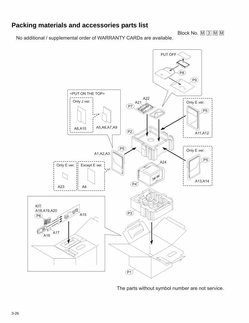
3-26
Packing materials and accessories parts listBlock No. M MM3
No additional / supplemental order of WARRANTY CARDs are available.
The parts without symbol number are not service.
PUT OFF
<PUT ON THE TOP>
A22A21
A15
A17A16
A24
P6
P2
P5
P7
P5
P5
P9
P1
P3
P4
P8
A5,A6,A7,A9
A1,A2,A3
A8,A10
Only J ver.
KIT:
A18,A19,A20
A4A23
A13,A14
A11,A12
Only E ver.
Only E ver.
Except E ver.Only E ver.
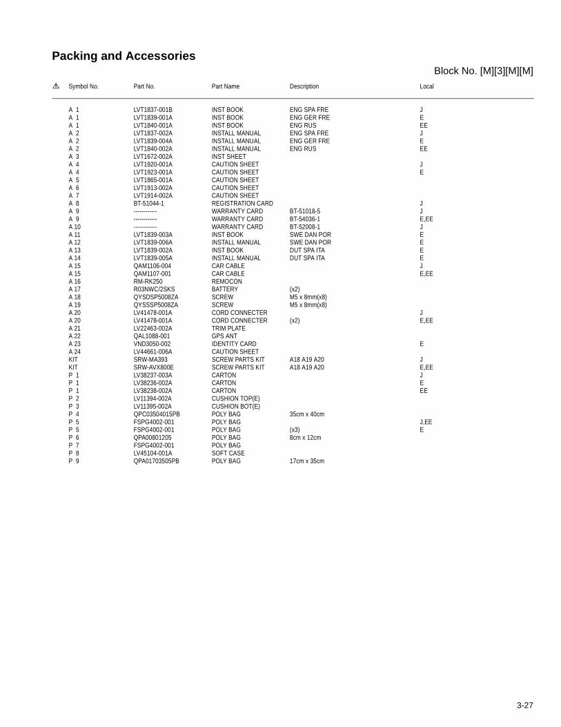
3-27
Packing and AccessoriesBlock No. [M][3][M][M]
Symbol No. Part No. Part Name Description Local
A 1 LVT1837-001B INST BOOK ENG SPA FRE JA 1 LVT1839-001A INST BOOK ENG GER FRE EA 1 LVT1840-001A INST BOOK ENG RUS EEA 2 LVT1837-002A INSTALL MANUAL ENG SPA FRE JA 2 LVT1839-004A INSTALL MANUAL ENG GER FRE EA 2 LVT1840-002A INSTALL MANUAL ENG RUS EEA 3 LVT1672-002A INST SHEETA 4 LVT1920-001A CAUTION SHEET JA 4 LVT1923-001A CAUTION SHEET EA 5 LVT1865-001A CAUTION SHEETA 6 LVT1913-002A CAUTION SHEETA 7 LVT1914-002A CAUTION SHEETA 8 BT-51044-1 REGISTRATION CARD JA 9 ------------ WARRANTY CARD BT-51018-5 JA 9 ------------ WARRANTY CARD BT-54036-1 E,EEA 10 ------------ WARRANTY CARD BT-52008-1 JA 11 LVT1839-003A INST BOOK SWE DAN POR EA 12 LVT1839-006A INSTALL MANUAL SWE DAN POR EA 13 LVT1839-002A INST BOOK DUT SPA ITA EA 14 LVT1839-005A INSTALL MANUAL DUT SPA ITA EA 15 QAM1106-004 CAR CABLE JA 15 QAM1107-001 CAR CABLE E,EEA 16 RM-RK250 REMOCONA 17 R03NWC/2SKS BATTERY (x2)A 18 QYSDSP5008ZA SCREW M5 x 8mm(x8)A 19 QYSSSP5008ZA SCREW M5 x 8mm(x8)A 20 LV41478-001A CORD CONNECTER JA 20 LV41478-001A CORD CONNECTER (x2) E,EEA 21 LV22463-002A TRIM PLATEA 22 QAL1088-001 GPS ANTA 23 VND3050-002 IDENTITY CARD EA 24 LV44661-006A CAUTION SHEETKIT SRW-MA393 SCREW PARTS KIT A18 A19 A20 JKIT SRW-AVX800E SCREW PARTS KIT A18 A19 A20 E,EEP 1 LV38237-003A CARTON JP 1 LV38236-002A CARTON EP 1 LV38238-002A CARTON EEP 2 LV11394-002A CUSHION TOP(E)P 3 LV11395-002A CUSHION BOT(E)P 4 QPC03504015PB POLY BAG 35cm x 40cmP 5 FSPG4002-001 POLY BAG J,EEP 5 FSPG4002-001 POLY BAG (x3) EP 6 QPA00801205 POLY BAG 8cm x 12cmP 7 FSPG4002-001 POLY BAGP 8 LV45104-001A SOFT CASEP 9 QPA01703505PB POLY BAG 17cm x 35cm

Contents
Block diagram
Standard schematic diagrams
Printed circuit boards
2-1
2-3
2-8 to 10
DVD-ROM No.SML2008Q2
SCHEMATIC DIAGRAMSNAVIGATION/DVD RECEIVER
No.MA427SCH<Rev.001>
2008/8
KW-NX7000J,KW-NX7000EKW-NX7000EE
COPYRIGHT 2008 Victor Company of Japan, Limited.
Lead free solder used in the board (material : Sn-Ag-Cu, melting point : 219 Centigrade)
Lead free solder used in the board (material : Sn-Cu, melting point : 230 Centigrade)
Only for KW-NX7000E
Only for KW-NX7000J

! Burrs formed during molding may be left over on some parts of the chassis. Therefore,
pay attention to such burrs in the case of preforming repair of this system.
Safety precaution
! Please use enough caution not to see the beam directly or touch it in case of an
adjustment or operation check.
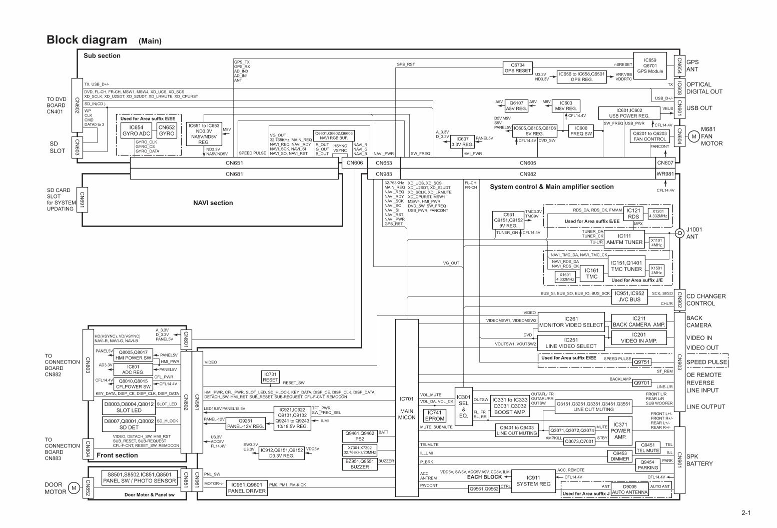
2-1
Block diagram (Main)
SD_IN(CD )
VIDEO
BATTQ9461,Q9462
PS2
VDD5V, SW5V, ACC5V,A9V, CD8V, ILMI
TFT_PWRSW_FREQ_SEL
TUNER_ON
IC921,IC922
Q9131,Q9132
Q9241 to Q9243
10/18.5V REG.
ILMI
SW3.3VU3.3V VDD5V
IC931
Q9151,Q9152
9V REG.
IC912,Q9151,Q9152
D3.3V REG.
TMC3.3VTMC9V
CFL14.4V
LED18.5V,PANEL18.5V
PANEL-12V Q9251
PANEL-12V REG.
X12014.332MHz
X16014.332MHz
X15014MHz
X11014MHz
X7301,X730232.768kHz/20MHz
Sub section
System control & Main amplifier section
Front section
IC111
AM/FM TUNER
IC151,Q1401
TMC TUNERIC161
TMC
IC701
MAIN
MICON
IC301
SEL
&
EQ.
IC331 to IC333
Q3031,Q3032
BOOST AMP.
Q3151,Q3251,Q3351,Q3451,Q3551
LINE OUT MUTING
Q9401 to Q9403
LINE OUT MUTINGQ3071,Q3072,Q3074
IC121
RDS
D9005
AUTO ANTENNA
IC371
POWER
AMP.
TU-L/R
ST_REM
FL, FRRL, RR
OUTAFL/ FROUTARL/RROUTSW
OUTSW
BACKLAMP
FRONT L+/-FRONT R+/-REAR L+/-REAR R+/-
VOL_MUTE
STBY
J1001
ANT
SPK
BATTERY
CN
901
TUNER_DATUNER_CK
RDS_DA, RDS_CK, FM/AM
NAVI_TMC_DA, NAVI_TMC_CK
MPX
AUTO ANT
ACC, REMOTE
CFL14.4V
ANT
ACCANTREM
IC951,IC952
JVC BUS
BUS_SI, BUS_SO, BUS_IO, BUS_SCK SCK, SI/SO
BUZZER
CN
902
IC608
LINE OUTPUT
PM0, PM1, PM-KICKMOTOR+/-
IC731
RESETRESET_SW
IC741
EPROM
VOL_DA, VOL_CK
MUTE, SUBMUTE MUTE
REVERSE
OE REMOTE
AMPKILL
P_BRK
TEL
ILL
PARK
ILLUMI
Q9561,Q9562
Q3073,Q7001TELMUTE
IC961,Q9601
PANEL DRIVER
BZ951,Q9551
BUZZER
Q9451
TEL MUTEQ9453
DIMMERQ9454
PARKING
Q9701
SPEED PULSESPEED PULSEQ9751
IC911
SYSTEM REG
CFL14.4V
CFL14.4V
EACH BLOCK
Used for Area suffix E/EE
Used for Area suffix J/E
Used for Area suffix J
VIDEO, DETACH_SW, HMI_RSTSUB_RESET, SUB-REQUESTCFL-F-CNT, RESET_SW, REMOCON
HMI_PWR, CFL_PWR, SLOT_LED, SD_HLOCK, KEY_DATA, DISP_CE, DISP_CLK, DISP_DATADETACH_SW, HMI_RST, SUB_RESET, SUB-REQUEST, CFL-F-CNT, REMOCON
CFL_PWR
OPTICAL
DIGITAL OUTC
N654
GPS
ANT
CN
803
CN
802
CN
981
PNL_SW
CN
903
CD CHANGER
CONTROL
FL-CHFR-CH
CHL/R
KEY_DATA, DISP_CE, DISP_CLK, DISP_DATA
CFL14.4VCFL14.4V
Q8010,Q8015
CFLPOWER SW
HMI_PWR
PANEL5V
PANEL5VPANEL5V
SLOT_LED
Q8005,Q8017
HMI POWER SW
AD3.3V IC801
ADC REG.
LINE-L/R
FRONT L/RREAR L/RSUB WOOFER
LINE INPUT
Used for Area suffix E/EE
CTRLPWCONT
DVD, FL-CH, FR-CH, MSW1, MSW4, XD_UCS, XD_SCSXD_SCLK, XD_U2SDT, XD_S2UDT, XD_LRMUTE, XD_CPURST
XD_UCS, XD_SCSXD_U2SDT, XD_S2UDTXD_SCLK, XD_LRMUTEXD_CPURST, MSW1MSW4, HMI_PWRDVD_SW, SW_FREQUSB_PWR, FANCONT
CN605
CN982
CN606 CN653
CN983
CN651
CN681
CN
801
CN607
WR981
CN
851
CN
961
Door Motor & Panel sw
S8501,S8502,IC851,Q8501
PANEL SW / PHOTO SENSOR
CN
852
CN
804
DOOR
MOTORM
CN
602
USB_D+/-
TXTX, USB_D+/-
VIDEOMSW1, VIDEOMSW2
VOUTSW1, VOUTSW2
WPCLKCMDDATA0 to 3 C
N604
CN
601
Q6201 to Q6203
FAN CONTROL
IC659
Q6701
GPS Module
FANCONT
HMI_PWR
M681
FAN
MOTOR
M
Q6107
A5V REG.
A5V A9V
nSRESETGPS_RST
IC607
3.3V REG.
A_3.3VD_3.3V
D5V,M5VS5VPANEL5V
PANEL5VDVD_SW
IC603
M8V REG.
IC606
FREQ SW
Q6704
GPS RESET
M8V
CFL14.4VIC605,Q6105,Q6106
5V REG.
U3.3VND3.3V
VRF,VBBVDDRTC
IC656 to IC658,Q6501
GPS REG.
CFL14.4V
ND3.3VNA5V,ND5V
U3.3VACC5VFL14.4V
A_3.3VD_3.3VPANEL5V
NAVI_RNAVI_GNAVI_B
IC651 to IC653
ND3.3V
NA5V/ND5V
REG.
USB_PWRSW_FREQ
IC601,IC602
USB POWER REG.
VBUS USB OUT
D8003,D8004,Q8012
SLOT LED
SD_HLOCKD8007,Q8001,Q8002
SD DET
SD
SLOT
CN
603
CN
691
CFL14.4V
Q6601,Q6602,Q6603NAVI RGB BUF.
IC654
GYRO ADC
CN652
GYRO
NAVI section
VG_OUT32.768KHz, MAIN_REQNAVI_REQ, NAVI_RDYNAVI_SCK, NAVI_SINAVI_SO, NAVI_RST
32.768KHzMAIN_REQNAVI_REQNAVI_RDYNAVI_SCKNAVI_SONAVI_SINAVI_RSTNAVI_PWRGPS_RST
SD CARD
SLOT
for SYSTEM
UPDATING
R_OUTG_OUTB_OUT
HD(HSYNC), VD(VSYNC)NAVI-R, NAVI-G, NAVI-B
TO DVD
BOARD
CN401
TO
CONNECTION
BOARD
CN882
TO
CONNECTION
BOARD
CN883
HSYNCVSYNC
GYRO_CLKGYRO_CSGYRO_DATA
SPEED PULSE
Used for Area suffix E/EE
NAVI_RDS_DANAVI_RDS_CK
IC251
LINE VIDEO SELECT
IC261
MONITOR VIDEO SELECT
IC201
VIDEO IN AMP.
IC211
BACK CAMERA AMP.
VIDEO IN
BACK
CAMERA
VIDEO OUT
VIDEO
DVD
VG_OUT
NAVI_PWR
M8V
SW_FREQ
GPS_TXGPS_RXAD_IN0AD_IN1ANT

2-2
Block diagram (DVD & Panel)
TPX1, TPX2TPY1, TPY2TPKEY1, TPKEY2
1.8V IC472
1.8V REG.
AD3.3V
X401
10MHz
X5001
16.5MHZ
X5002,IC502
9.6MHZ
CN
502
CN
403
Connection section
IC452
Q402,Q403
RESETSUB_RST
SUB_RESET
DETACH_SW
SUBRST
CN
503
CN
881
CN
883
CN
551
CN
501
CN
401
IC451
Q401
MICON
IC411,IC412
GANMA
IC501
IC503
IC504
Q5001
HMI
IC471,IC473
AD CONVERTER
LCD
MODULE
TOUCH
PANEL
V0 to 10
Panel section
Key, Lighting & Remocon
LCD Display control & Touch senser
S551 to S559
KEYMATRIX
D553 to D563
LIGHTING DISPLAY
IR0 to 5, IG0 to 5, IB0 to 5, HOUT, VOUT, DEN, CLK, CSY, OE
SDA, SCL
CE
IC551
REMOCON
REMOCON
M-LED M-LED
LED-ONDIMMERSUB-REQUEST
LED-ONDIMMERPOWERLEDLED-B-3LED-B-4-1 to 2
M-LEDM-SENSE
KEYIN1, KENIN2, KEY1, KEY2KEY1, KEY2KEYIN1, KENIN2
IC402
Q4001 to Q4007
VCOM DRIVER
Q508 to Q511
TOUCH SENSE AMP.
IC513,Q506,Q507
LED DRIVER
VCOMCOM_DCCOMAC
IC461 to IC464
Q4605,Q4607
CFL CTL & DRIVER
D551
M LED
POWERLEDRESETSW, POWERLED, REMOCON
D552
POWER LED
BL-ON, CFL-CTL, OZ_PWR
CFL-F-CNT
VIDEO, KEYDATA, DISPCE, DISPCLK, DISPDATA, HMI-RST
LED-B-3LED-B-4-1 to 2
LED-B-3LED-B-4-1 to 2
D0 to 15, A0 to 21, CS, WE, FOE, FRST IC512
FLASH ROM
Q8801 to Q8805
DIMMER CONTROL
S8801
DETACH SW
SDDATA0 to 15, SDAD0 to 11, SDBA0/1SDM0, SDM1, SDCKESDWE, SDCS, SDRAS, SDCAS, MEMCLK IC511
SDRAM
VIDEO, HMI_RSTSUB_RESETSUB-REQUESTCFL-F-CNTRESET_SW, REMOCON
X354,IC308
48MHz
USBCLK
D1.2V D2V
MA0 to 11, MDQ0 to 15, DQM0/1BA0, BA1, MCK, NWENCSM, NCAS, NRAS IC399
SDRAM
UCS, SCS, SCLK, U2SDT, S2UDT, LRMUTE
A, B, C, D, E, F, RF+/-, LPC1, LPC2
CD/DVD
CD VRDVD VR
Q105 to Q107
HFVCHFM VCCQ8,Q9
Q103,Q104
Q101,Q102
D9,D11
PHOTO SENSOR
EXADT0 to 15EXADR16 to 20NEXOE, NEXCE, NEXWE IC398,IC501,IC502
FLASH ROM
IC302
1.2V REG.
D3.3V
P3.3V
S3.3V D4VIC3
3.3V REG.
EPWPI2CSCL, I2CSDT
IC400
DAC
AOUT3, DAC0CS, DCLK, DDATA, PCMCLK, BCK, LRCLK, DACPDN
IC1
Q2
DRIVER
F+/-T+/-
M
M
LOAD MOTOR
TO SUB BOARD
CN602
CN
882
TO FRONT BOARD
CN803
TO FRONT BOARD
CN804
LDO+/-
REST
H1+/-, H2+/-, H3+/-SLED1+/-, SLED2+/-SM1 to SM3
TRVSW
LM, FG, DRVCNT/DRVMUTETRDRV, FODRVSPDRV, PRTOUTSL1IN, SL2IN
SPINDLE MOTOR
REST SW
CN
1
FL-CHFR-CH
D6,D7
IR LED
Q4,Q7
PHOTO SW
S1
DETECT SW
M5V
ACC5V
CN
101
DVD section
PICK UP
IC301
IC7
DV5
FOCUS
&
TRACKING
COIL
LPCO1DVDLDCURDVD LD
LPCO2CDLDCURCD LD
SW3
SW1
SW1, SW4
IC481
EPROM
X351
27MHz
Q301
Q302SW4
CPURST
CN
401
CN
2
/FL_RST
TX, USB_D+/-
DAC4 (DVD)
IC307
IPOD DECODER
X353
32.768kHz
CP_RDY, RST_II2CSDT_I, I2CSCL_I
A3.3VAD3.3VD3.3VU3.3VACC5VPANEL5VCFL14.4VPANEL18.5VLED18.5V
NAVI-R, NAVI-G, NAVI-B, HD, VD
KEYDATA, DISPCE, DISPCLK, DISPDATANAVI-R, NAVI-G, NAVI-B, HD, VD
R0 to 5, G0 to 5, B0 to 5, HIN, VIN, DVCLK, V-RST
DATA0 to 3, WP, CD, CLK, CMD
RESETSW
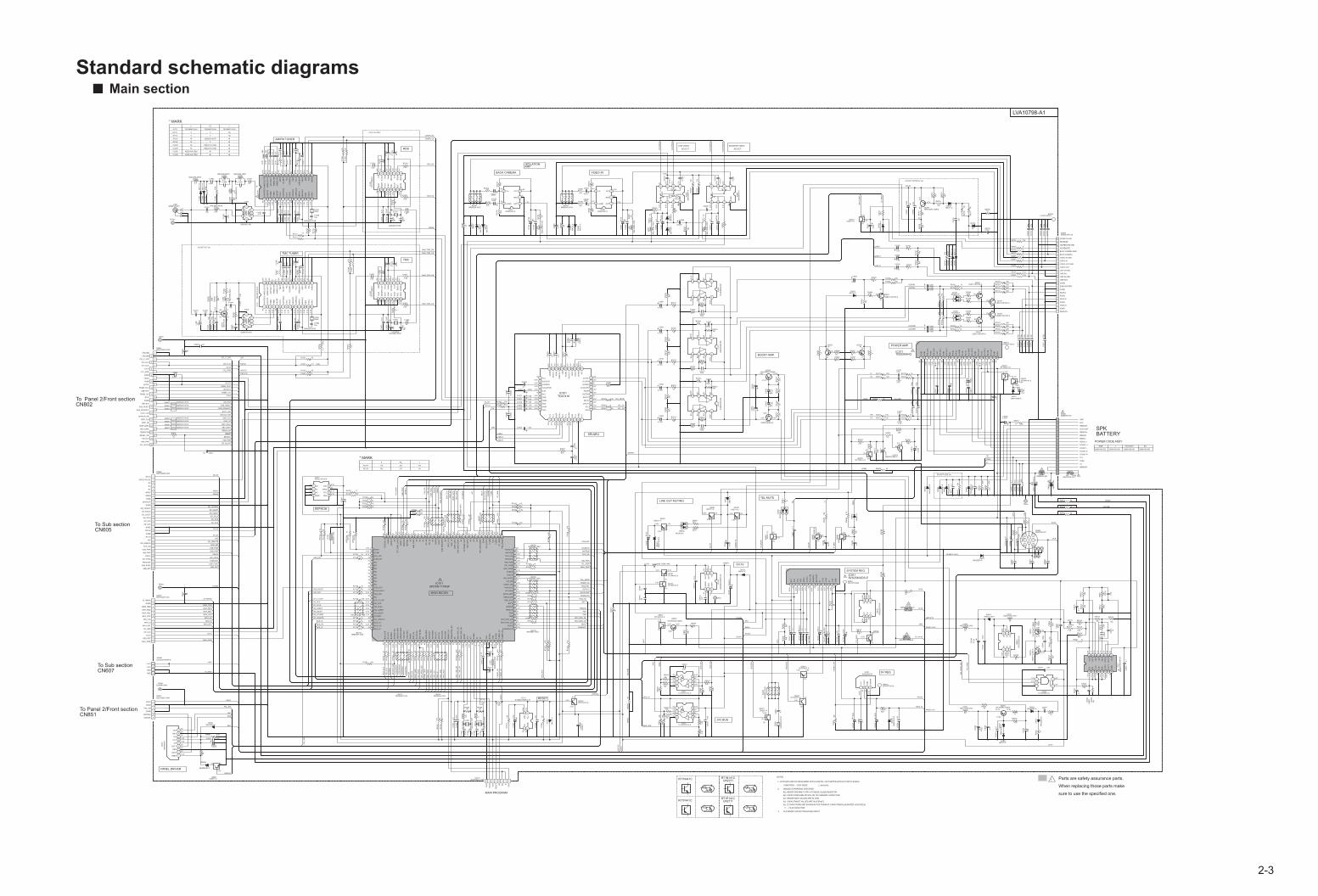
2-3
Standard schematic diagrams
UN2111
UN2211
0V
0V
5.2V
5.2
V
0V
1.8
V
4.9
V
9.0
V
1.6
V
1.6
V
1.6
V1.5
V
3.2
V
1.6
V
0V
1.6
V
1.5
V
0V
0V
0.1
V
0V
0V
1.6
V
3.2
V
9.0
V
3.2
V
3.2
V
3.9
V 0V
3.9
V
0.4
V
0.1
V 0V
0V
6.7
V
0.4
V
3.9
V
3.6
V
6.7
V
0.8
V
0V
5.6
V
9.0
V
0V
2.0
V
5.7
V
9.0
V
4.1
V
0V
3.9
V
7.0
V
1.0
V
3.1
V
0V
2.2
V
9.0
V
NCB31HK-102X NINI
NININCB31HK-102X
NI NDC31HJ-330X NI
NI NDC31HJ-330X
NI
NINI
NI
NI QAX0263-001Z
0
C1609
C1209
C1207
C1208
X1201
R1202
0
EE
0
TEF6606T/V2-X
EE J
47k
33k 27k
15k
NIR7215
R7214 22k
* MARKE
0
TEF6601T/V2-X
15kR1111
R1112
E
0
* MARK
15k
J
TEF6606T/V2-XIC111
EXCEPT NX7000-J Ver.
EXCEPT EE Ver.
DVD
PARK
0V
0V
0.1V
9.0V
0V
H
0V
2.3V
-15.0V
0.1
V
3.3V
75DRV
-10.1V
REAR R+
0V
0V
0V
9.0V
-9.4V
4.5V
FRONT R-
0V
5.0V
0V
0V
4.5V
H
0V
0V
3.2
V
4.5V
0V
4.4V
5.0V
3.3V1.6
V
4.5V
4.5V
1.0V
1.6
V
CONDITION --- DVD MODE.
0.1V
9.8
V
0V
0V
4.5
V
1.6
V
1.3
V
-12.8V
0V
3.3V
1.5
V
6.7
V
4.5
V
-15.0V
0V
0V
4.5
V
1.6V
3.9
V
5.0V
1.6V
4.5
V
0V
3.6
V
0V
4.5
V
14.4
V
6.7
V
9.0
V
0V
3.3
V
0.8
V
3.3V
BOOST AMP.
6.5V
0V
5.0
V
0V
0V
MAIN MICON
5.2
V
13.8V
3.9
V
5.8
V
0V
7.0
V
5.0V
0V
1.0
V
7.2
V
UNLESS OTHERWISE SPECIFIED.
5.2V
5.0V
0.1
V
3.1
V
2.
POWER AMP.
0V
AM/FM TUNER
2.5
V
0V
9.0
V
POWER CODE ASSY
LINE OUT MUTING
0V
6.6
V
0V
3.2
V
10k
0V
10.9V
0V
-0.1V
3.2
V
0V
13.7V
0V
3.3V
3.9
V
5.2V
2.7V
0V
0V
3.9
V
0V
7.8V
0V
0V
4.5
V
0.1
V
9.9
V
EEPROM
7.9V
0V
3.3V
0V
0V
7.4V
3.3V
4.5
V
0V
0V
3.2V
0V
0.5
V
5.7V
0V
RESET
FRONT R+
0V
0.4
V
3.3
V
0V
0V
TEL
0V
0V
5.0
V
3.3
V
3.3V
3.2V
2.8
V
0V
0.4
V
5.0
V
0V
3.3V
2.2
V
6.5V
0V
0V
3.3V
0V
9.0
V
2.2
V
0V
3.3V
SELECT
5.7
V
0V
VIDEO IN
3.3V
2.7
V
0V
5.6
V
BACK CAMERA
0V
3.3V
9.1
V
REAR L+
9.0
V
9.9
V
3.0V
0V
0V
3.2V
REAR R-
0V
0V
11.0V
3.1
V
GND
2.2
V
14.4V
0V
0V
ILL
0V
0V
2.0
V
0V
0V
0V
0V
0V
9.0
V
4.3V
0V
0V
3.3
V
4.6V
-9.4
V
0V
4.1
V
3.3
V
4.6V
0V
0V
0V
47k
0V
4.6V
9.0
V
0V
47k
0V
3.3
V
4.5V
-.-V
4.5
V
E/EE Ver.ONLY
0V
0V
5.0V
0V
0V
0V
0V
EXCEPT E/EE Ver.
5.0V
0V
4.8V
0V
0V
0V
7.0
V
0V
0V
0V
7.8V
0V
0V
0V
0V
1.1
V
0.4V
0V
0V
3.3V
3.3
V
RT1N141C
2.5
V
-9.4
V
7.0
V
2.3
V
3.3
V
3.2
V
10k
0V
-.-V
0V
3.3V
0.1V
0V
0V
13.8
V
4.5V
0.9
V
0V
3.2V
3.3
V
9.0
V
14.4
V
( ) AM MODE.
J
0V
3.3
V
0V
4.4
V
3.2
V
5.0V
QAM1106-001
3.3V
0V
0V
3.0
V
0V
0V
5.2V
0V
FRONT L+
0V
0V
REAR L-
3.0
V
0V
0V
0V
0V
3.3
V
4.5V
14.4
V
0V
0V
14.4
V
3.3
V
0V
4.5V
7.0
V
0V
7.0
V
0.3V
0V
0.5
V
3.3
V
7.0
V
0V
0.6
V
6.8
V
0V
0V
2.5
V
6.8
V
3.3
V
2.5
V
0V
0V
0V
0V
0V
0V
0V
0.4
V
0V
0V
0.5
V
0V
2.7V1.6
V
9.9
V
0V
5.0V
7.0
V
MONITOR VIDEO
1.7
V
9.9
V
0V
3.3
V
6.8
V
L
5.0V
0V
6.8
V
3.3
V
0V
L
47k
0V
0V
6.8
V
3.3
V
RT1P141C
3.1V
3.3
V
2.5
V
5.2
V
0V
0V
0V
L
0V
3.3
V
0V
QAM1106-004
0V
0V
0V
0V
H
3.0
V
3.2
V
0V
QAM1106-002
0V
0V
0V
0V
0.2
V
0V
0V
0V
ACC
0V
0V
0V
0V
AUTO ANT
1.7
V
0V
0V
0V
0V
1.3
V
0V
3.3
V
-9.4
V
0V
3.3V
1.6
V
JVC BUS
1.3
V
0.5
V
0V
0V
0V
PANEL.DRIVER
0V
0V
0V
0V
4.5
V
0V
3.3V
9.0
V
0.1
V
0V
4.5
V
8.9
V
4.5V
0V
0V
D3.3V
0V
4.5V
0V
3.2
V
4.5
V
E/EE A/U/UN/UT
9.0V
3.3V
3.2
V
7.0
V
9.0
V
4.5
V
EU
9.6V
4.8
V
0V
0V
0V
QAM1106-003
9.8V
0V
2.8
V
0.4
V
1.6V
MEMORY
5.8V
4.5
V
1. VOLTAGES ARE DC-MEASURED WITH A DIGITAL VOLT METER WITHOUT INPUT SIGNAL
ACC5V
0V
1.6V
SEL&EQ
0V
0V
0V
NI STANDS FOR NOT MOUNTED PARTS
-12.2V
3.2V
5.2
V
0V
REMOTE
0V
3.
3.3V
3.3V
2.5
V
0V
FRONT L-
0V
TMC
3.3V
LVA10798-A1
2.5
V
7.0
V
0V
RDS
0V
3.2V
ALL E.CAPACITORS ARE SHOWN IN THE FORM OF CAPACITANCE(uF)/RATED VOLTAGE(V)
1.3
V
9.8
V
TMC TUNER
ALL CAPACITANCE VALUES ARE IN uF(P=pF)
8.0
V
0V
0V
TEL MUTE
9.9
V
0V
9.9
V
3.0V
0V
9.8
V
MAIN PROGRAM
3.2V
RT1P441C
0V
9.8
V
ISOLATION
ALL CAPACITORS ARE 50V,25V OR 16V CERAMIC CAPACITOR.
RT1N441C
0V
0V
0V
1.5
V
ALL RESISTORS ARE 1/10W +5% METAL GLAZE RESISTOR.
AMP
9.8
V
3.3V
ALL RESISTANCE VALUES ARE IN OHM.
0V
1.6
V
LINE VIDEO
9V REG
0V
0V
2.3V
0V
SELECT
0V
10k
0.3V
SYSTEM REG
3.1V
1.6
V
L
47k
F --- FILM CAPACITOR
0V
3.1
V
0V
1.6
V
6dB
NOTES
2.9
V
0V
H
3.2
V
0V
3.2V
4.4V
1.5
V
10k
3.3V
0V
ALLGND
ALLGND
ALLG
ND
SCK
TU
NE
R_O
N
AGND
TMC9V
TUNER_CK
TUNER_DA
DG
ND
S1GND
S1GND
U3.3
V
U3.3V
AMPKILL
RE
SE
T
AM
PK
ILL
VGND
REMOCON
ST
_R
EM
32.7
68K
HZ
NA
VI_
RE
Q
NA
VI_
RD
Y
MA
IN_R
EQ
SU
B_R
EQ
UE
ST
KE
Y_D
ATA
BACKLAMP
ILL
PARK
TF
T_P
WR
SW
_F
RE
Q_S
EL
VDD5V
VDD5V
VDD5V
MGND
D10V
RR
FR
RL
FL
A9V
FL-CH
FR-CH
NAVI_TMC_CK
OUTAFL
TMC3.3V
SW3.3V
A9V
TMC3.3V
TMC9V
14.4V
CFL14.4V
CFL_F_CNT
14.4V
NAVI_TMC_DA
NAVI_RDS_DA
NAVI_RDS_CK
FM/AM
RDS_CK
RDS_DA
US
B_F
UN
C
DIS
P_C
LK
DIS
P_C
E
DIS
P_D
ATA
BUS_SI
BUS_SO
XD_S2UDT
XD_U2SDT
XD_SCS
BUS_IO
XD_SCLK
BU
S_S
CK
XD_LRMUTE
RESET
CFLGND
U3.3V
PANEL-12V
ACC5V
CFL_PWR
PANEL18.5V
D10V
LED18.5V
REMOCON
SLOT_LED
DETACH_SW
NAVI_SI
NAVI_SO
NAVI_SCK
NAVI_RDY
NAVI_REQ
MAIN_REQ
NAVI_RST
U3.3V
NAVI_PWR
LED18.5V
PANEL18.5V
BUS_IO
REMOTE14.4V
ACC5V
SW5V
SD
_IN
HMI_PWR
NAVI_PWR
CFL_PWR
AMPKILL
SW
_F
RE
Q_S
EL
SUBMUTE
MUTE
P_B
RK
AC
C
BU
S_S
CK
DVD_SW
PWCONT
VOL_MUTE
USB_DET
XD_CPURST
CFL_F_CNT
HMI_RST
SUB_RESET
M8V
SW
3.3
V
VO
L_D
A
VO
L_C
K
AC
C
PN
L_S
W
BU
ZZ
ER
PMKICK
PM1
PM0
SD_HLOCK
SD
_H
LO
CK
SW_FREQ
HMI_PWR
USB_FUNC
USB_DET
SD_IN
OUTARR
OUTARL
OUTAFR
PNL_SW
NAVI_RDS_CK
SW
_F
RE
Q
NAVI_RDS_DA
TELMUTE
ILLU
MI
DETACH
NA
VI_
SO
US
B_P
WR
NA
VI_
SI
RDS_CK
TUNER_ON
XD
_U
CS
NA
VI_
SC
K
BATT
DE
TA
CH
_S
W
NA
VI_
RS
T
FANCONT
VID
EO
MS
W1
VID
EO
MS
W2
VO
UT
SW
1
MS
W4
NA
VI_
TM
C_D
A
VO
UT
SW
2
NA
VI_
TM
C_C
K
ANTREM
MS
W1
BU
ZZ
ER
FM
/AM
TU
NE
R_C
K
TF
T_P
WR
RD
S_D
A
TU
NE
R_D
A
SLO
T_LE
D
XD_CPURST
DISP_CE
SUB_RESET
SUB_REQUEST
HMI_RST
KEY_DATA
DISP_CLK
DISP_DATA
HMI_PWR
TF
T_P
WR
PANEL-12V
FANCONT
FL-CH
MSW4
FR-CH
USB_PWR
MSW1
XD_LRMUTE
XD_U2SDT
XD_UCS
XD_SCS
DVD_SW
XD_S2UDT
XD_SCLK
32.768KHZ
A9V
DETACH
CFL14.4V
SU
BM
UT
E
BUS_SCK
SI/SO
SW5V
BA
TT
PW
CO
NT
BA
CK
LA
MP
ST
_R
EM
M8V
SC
K
SI/S
OV
OU
TS
W2
BU
S_S
I
LINE-L
LINE-R
LINE-G
CHL
CHR
MU
TE
LINE-G
VID
EO
MS
W1
VO
UT
SW
1
VID
EO
MS
W2
BU
S_S
O
P_B
RK
PM1
PMKICK
PM0
TE
L
ILLU
MI
LINE-R
LINE-L
VOL_MUTE
CH
R
AN
TR
EM
VOL_CK
VOL_DA
ILL
TE
LM
UT
E
TEL
CH
L
PA
RK
!
!
!
!
!
!
!
!
!
!
!
!
C9054
0.0
01
R9302
22k
AM
RF
DE
C
1
AM
RF
IN
2
FM
IN2
3
FM
IN1
4
GN
DR
F
5
VC
C2
6
AM
RFA
GC
7
LO
UT
8
RO
UT
9
GN
DA
UD
10
AM
IFA
GC
2
11
MP
XIN
12
MP
XO
UT
13
RS
SI
14
XTA
L2
15
XTA
L1
16
GN
DD
17
SC
L
18
SD
A
19
VR
EF
20
VR
EG
SU
P
21
VC
C1
22
GN
D
23
VC
OD
EC
24
PLL
25
PLLR
EF
26
TE
ST
27
AM
SE
LIN
1
28
AM
SE
LIN
2
29
AM
IFA
GC
1
30
AM
SE
LO
UT
1
31
AM
SE
LO
UT
2
32
*IC
111
R1112 *R1111 *
VE
RS
ION
*R
7214
VE
RS
ION
*R
7215
NQ
L79G
M-4
70X
L2601
560
L11
01
0.4
7N
QL093K
-R47X
L1004
NQL79GM-220XL9251
22
NQL79GM-220XL9242
22
NQ
L79G
M-4
70X
L2101
4.7
NQL093K-4R7XL1002
0.2
2N
QL093K
-R22X
L1402
NQ
L79G
M-4
70X
L2501
560
L11
02
NI
L1401
1.8
NQL093K-1R8XL1005
0.47
NQL093K-R47XL1003
0.22
NQL093K-R22XL1001
NQ
L79G
M-4
70X
L2001
QQR0703-001L9001
NI
D9752
R9757
NI
5678
4321
NRZ0065-301XRA201
5678
4321
NRZ0065-301XRA202
1kR7115
R1406
0
1/8
W
R1554
4.7
C3007
0.0
56
R9151
NI
C9155
NI
C9154
NI
RT1P441C-XQ7001
3.3
kR
7095
R35552.2K
R34552.2K
R32552.2K
R31552.2K
R33552.2K
0.001C9703
C1406
0.0
1
47k
R7220
1k
R7016
1k
R7015
1k
R7014
1k
R7077
47kR7222
47kR7221
R3554 200
R3454 200
R3254 200
R3154 200
R3354 200
C9007
0.0
1
C9006
0.0
1
C1002
22p
C1001
15p
R1405
0
R1404
82k
R1403
100k
87
64 3
21
QQR1813-001
T1401G2
SG1
D
3S
K195-W
Q1401
R925510
NIB9131
+
-
+
-
+
-
+
-
+
-
+
-
FUSE15A
F9001
QMFZ039-150-T
QA
X0932-0
01Z
X7302
20M
Hz
QAX0263-001Z
X1601
4.332MHz
QAX0263-001Z
X1201
*
QAX0928-001Z
X15014MHz
QAX0928-001Z
X11014MHz
QA
N0023-0
01Z
BZ
951
QA
X0401-0
01
X7301
32.7
68kH
z
TP983
TP901
TP101
TP981
QZW0010-001PP961
LV43373-002ABK911
LV44477-001ABK931
LV43967-001ABK371
LV37970-001ABK903
NA
D0028-1
03X
TH
721
5
6
7
8
4
3
2
1
NRZ0065-102XRA710
5678
4321
NR
Z0065-1
51X
RA
708
5678
4321
NR
Z0065-1
02X
RA
707
5
6
7
8
4
3
2
1
NRZ0065-102XRA706
5
6
7
8
4
3
2
1
NRZ0065-102XRA705
5678
4321
NRZ0065-102XRA703
5678
4321
NRZ0065-102XRA701
5
6
7
8
4
3
2
1
NRZ0065-102XRA704
5678
4321
NR
Z0065-1
02X
RA
709
5678
4321
NR
Z0065-3
92X
RA
951
12kR3234
R9453
10k
R1552 0
39
R2005
100k
R2004
1/8
W
R1503
22
0R2008
0R2007
NIR9705
R3203
47k
R3471 100
R3271 100
R2002
470
R9106
9.1
k
1/8W
R9001
1k
R3103
47k
R3104
0
0R2107
R2502
75
2.2kR3202
R3453 200R1401
100k
3.3
k
R3031
R3253 200
12k
R3134
R3153 200
R3353 200
470
R2001
R3372 1k
NI
R7079
100R7124
R1507
4.7
k
R1506
4.7
k
R11
06
4.7
k
R11
05
4.7
k
R3172 1k
R3472 1k
R3451 1k
R3272 1k
R3204
0
R9451
1k
R3072
10
R9455
10k
R1002
470k
R1001
470k
R2503
10k
12k
R3534
R2102
470
470R9402
R1553
0
R3076
10k
R9002
100k
12k
R3434
18k
R3533
R3332
47k
12kR3334
R9461
56k
1/8
W
R9004
2.2
k
R307547k
1/8
W
R9003
2.2
k
R3074
47k
R3331
1k
R3232
47k
R323318k
R9454
4.7
k
R3371 100
R3171 100
R3231
1k
R3132
47k
R9102
NI
R3252
47k
R2604
3.3
k
R2603
180
4.7
k
R3034
R3531
1k
R3105
150
0R2108
R3205
150
R3552
10k
R3553 200R3551
1k
R9704 10k
22K
R9753
10k
R9755
820
R9752
22k
R9754
390
R9751
R3071
2.2k
18k
R3133
R9756
100
1kR7058
1kR7059
100k
R2003
R9056
NI
R9053 NI
R9052 NI
R9051 NI
R9055 NI
1k
R7013
R3432
47k
R3532
47k
18k
R3433
R3452
47k
R3431
1k
R3352
47k
R3152
47k
R333318k
R3073
27k
R3131
1k
0R2505
0R9703
R9462
18k100R7128
470R2101
10k
R7216
R9104
47k
R9103
33k
R1402
390k
R3055
0
R3056
0
10kR7213
10kR7212
R111
4
47k
R111
3
47k
R2601
10
NI
R3052
NI
R3054
NI
R3053
NI
R3032
R1152 NI
1/8WR1551 4.7
R1151 NI
NI
R3051
R3201
47k
R9218
8.2k
R9216
10k
R3005 2.2k
R9245
150
R1201
2.2k
R3004 0
R1602
0
R1202
*
R1203
2.2k
R9213
33k
R9101
NI
R9246
10
R9243
33k
R9215
5.6
k
R9244
33k
R3003 100
R9219
680
R9214
33k
R9212
100k
R9220
120k
R9221
33k
R9252
10
R925110
R9211
56k
R3101
47k
R9241 47
R1502
4.7
k
R9217
1.2k
R9242
470
R3001
470
0R9253
4.7k
R9254
470R9401
470
R9702
R9203
1.2k
100k
R2103
R2105
39
R2006
10
R3106 470
R2501
10
1/8
W
R11
02 2
2
R11
01
4.7
k
R3206 470
R1603
2.2k
R9301680
1k
R9602
2.2kR9601
R9054 NI
R1601
2.2k
R9204
15k
0
R2602
R9105
4.7
k
R9801
1k
R2106
10
2.2kR3102
1k
R7004
R9503
10k
4.7kR7209
R9506
68k
1k
R7002
1kR7117
R9507
3.9
k
4.7
kR
7217
4.7kR7211
R9508
6.8
k
47k
R7205
1kR7127
R7353
2.2
k
47kR7201
R7302
47k
2.2
kR
70661
00
R7089
R7305
0
4.7kR7210
47k
R7203
R9504
22k
R7301
47k
22kR7206
R7402 100
47k
R7204
0R7048
100
R7038
R9510100
47k
R7202
1kR7047
R9505100
R7401 0
2.2
k
R3033
100
R7037
R950922k
100
R7025
R9502
6.8
k
220
R7088
R735210k
R7751
470
R9511
68k
47k
R7102
R9501
3.9k
1k
R7012
1kR7050
1kR7125
1kR7116
0R7042
R7354
10k
R9005
10k
1kR7049
1kR7106
1k
R7011
47kR7207
R9512
22k
0R7041
2.2
kR
7009
270
R9701
1kR7126
1kR7105
1k
R7001
0R
7010
R7306NI
R7303
47k
R2504
1M
47kR7208
100
R7024
2.2kR7119
R7304NI
R3151 1k
1k
R7096
R3351 1k
R3251 1k
100k
R2104
R9131
10kUN2211-X
Q9132
RT1N441C-XQ9461
UN2211-XQ9601
RT1N441C-XQ9562
RT1N441C-XQ3071
UN
22
11
-XQ
9451
RT1N441C-XQ9152
RT1N441C-XQ3073
UN2211-XQ9701
UN2211-XQ9551
UN
22
11
-XQ
9454
RT1P441C-XQ9561
RT1P441C-XQ3072
UN2111-XQ9401
UN2111-XQ9402
UN2111-XQ9403
RT1P441C-XQ9151
ISA1530AC1/QR/XQ9751
2SD2114K/VW/-X
Q3551
2SD601A/QR/-XQ3031
2SD2114K/VW/-XQ3251
2SD601A/QR/-XQ3074
2S
D601A
/QR
/-X
Q9242
2SD2114K/VW/-XQ3451
2SD2114K/VW/-XQ3351
2S
D601A
/QR
/-X
Q9453
2SD2114K/VW/-XQ3151
NIQ3051
ISA1530AC1/QR/XQ9251
ISA1530AC1/QR/XQ3032
ISA
1530A
C1/Q
R/X
Q9241
ISA1530AC1/QR/X
Q9462
NIQ3052
NQL79GM-100XL9151
10
NQLD7EM-470XL9241
47
NQ
R0022-0
05X
L7001
NQR0251-001XK9802
NQR0251-001XK9807
NQR0251-001XK9801
NQR0251-001XK9803
NQR0251-001XK9806
NQR0251-001XK9805
NQR0251-001XK9804
BUS_SI128
BUS_SO127
BUS_IO126
XD_LRMUTE125
CPURST124
XD_S2UDT123
XD_U2SDT122
XD_SCLK121
XD_SCS120
CFL_F_CNT119
NC118
HMI_RST117
SUB_RESET116
GPS_RST115
NC114
NC113
NC112
NC111
NC110
NC109
NC108
NC107
USB_DET106
PNL_SW105
TEMP104
AREA103
TE
ST
KE
Y1
102
AV
SS
101
AV
RE
F0
100
NC
99
TF
T_P
WR
_C
ON
T
98
AV
RE
F1
97
US
BP
WR
96
AM
PK
ILL
95
NC
94
US
B_F
UN
C
93
NC
92
NC
91
NC
90
I2C
_D
A
89
I2C
_C
L
88
NC
87
MS
W4
86
MS
W1
85
SU
B_R
EQ
UE
ST
84
NC
83
DIS
P_C
LK
82
DIS
P_C
E
81
DIS
P_D
ATA
80
EX
T_N
AV
I_D
ATA
79
NC
78
32.7
68kH
z_O
UT
77
KE
Y_D
ATA
76
NC
75
NC
74
NC
73
NA
VI_
BA
CK
LA
MP
72
SD
IN
71
SD
_H
LO
CK
70
ILLU
MI
69
AC
C
68
P_B
RK
67
ST
_R
EM
66
PN
L_M
OD
E
65
TELMUTE 64
ANTREM 63
DVD_SW 62
PWCONT 61
HMI_PWR 60
CFL_PWR 59
NAVI_PWR 58
EVDD1 57
EVSS1 56
VOL_MUTE 55
FM_SW 54
TUNER_ON 53
FANCONT 52
DETACH 51
BACKLAMP 50
REMOCON 49
RDS_SCK 48
BATT 47
BUSINT 46
PMKICK 45
PM1 44
PM0 43
NAVI_RDS_DA 42
NAVI_RDS_CK 41
MUTE 40
SUBWMUTE 39
TU
NE
R_D
A
38
TU
NE
R_C
K
37
EV
DD
0
36
VD
D
35
EV
SS
0
34
VS
S
3332
X1
31
X2
30
FLM
D0
29
XT
1
28
XT
2
27
RE
SE
T
26
NA
VI_
TM
C_C
K
25
NA
VI_
TM
C_D
A
24
NC
23
DE
BA
G/P
RG
_D
A
22
DE
BA
G_C
K
21
NA
VI_
RS
T
20
NA
VI_
SC
K
19
NA
VI_
SI
18
NA
VI_
SO
17
NA
VI_
RE
Q
16
NA
VI_
RD
Y
15
MA
IN_R
EQ
14
NC
13
SW
fre
q S
EL
12
SLO
T L
ED
11
RD
S_D
A
10
FM
/AM
9
VO
UT
SW
2
8
VO
UT
SW
1
7
VID
EO
M S
W2
6
VID
EO
M S
W1
5
DE
TA
CH
SW
4
BU
ZZ
ER
3
XD
_U
CS
2
BU
S_S
CK
1
UPD78F1178GFIC701
IN2L44
IN3R43
IN3L42
IN4R41
IN4L40
N.C.39
Cref38
ACOUTSW37
ACINSW36
ACOUTR35
N.C.34
AC
INR
33
AC
OU
TL
32
AC
INL
31
VR
EF
OU
T
30
VD
D
29
AC
2IN
L
28
AC
2O
UT
L
27
FIL
OL
26
OU
TLF
25
OU
TLR
24
N.C
.
23
OUTRF 22
OUTRR 21
AC2INR 20
AC2OUTR 19
FILOR 18
OUTSW 17
SAOUT 16
MUTE 15
SACLK 14
SCL 13
SDA 12
N.C
.
11
GN
D
10
N.C
.
9
MIX
8
IN1R
+
7
N.C
.
6
IN1-
5
IN1L+
4
IN2R
3
N.C
.
2
N.C
.
1
TDA7416IC301
AM
RF
DE
C
1
AM
RF
IN
2
FM
IN2
3
FM
IN1
4
GN
DR
F
5
VC
C2
6
AM
RFA
GC
7
LO
UT
8
RO
UT
9
GN
DA
UD
10
AM
IFA
GC
2
11
MP
XIN
12
MP
XO
UT
13R
SS
I14
XTA
L2
15
XTA
L1
16
GN
DD
17
SC
L
18
SD
A
19
VR
EF
20
VR
EG
SU
P
21
VC
C1
22
GN
D
23
VC
OD
EC
24
PLL
25P
LLR
EF
26
TE
ST
27
AM
SE
LIN
1
28
AM
SE
LIN
2
29
AM
IFA
GC
1
30
AM
SE
LO
UT
1
31
AM
SE
LO
UT
2
32
TE
F6601T
/V2-X
IC151
GN
D
1
GN
D
2
FR
OU
T-
3
ST
BY
4
FR
OU
T+
5
Vcc1
6
RR
OU
T-
7
GN
D
8
RR
OU
T+
9
RE
F
10
RR
IN
11
FR
IN
12
S-G
ND
13
FL IN
14
RL IN
15
AC
-GN
D
16
RL O
UT
+
17
GN
D
18
RL O
UT
-
19
Vcc2
20
HS
D
25
GN
D
24
FL O
UT
-
23
MU
TE
22
FL O
UT
+
21
TB2926AHQIC371
CT
1
RT
2
+IN
1
3
-IN
1
4
FB
1
5
DT
C1
6
OU
T1
7
GN
D
8
Vcc
9
OU
T2
10
DT
C2
11
FB
2
12
-IN
2
13
+IN
2
14
SC
P
15
Vre
f
16
BA
9743A
FV
-X
IC921
RD
SID
1
RD
DA
2
Vre
f
3
MP
XIN
4
Vdda
5
Vssa
6
FLO
UT
7
CIN
8
TE
ST
9
MO
DE
10
Vssd
11
Vddd
12
XIN
13
XO
UT
14
RS
T
15
RD
CL
16
LC
72725K
M-X
IC121
RD
SID
1
RD
DA
2
Vre
f
3
MP
XIN
4
Vdda
5
Vssa
6
FLO
UT
7
CIN
8
TE
ST
9
MO
DE
10
Vssd
11
Vddd
12
XIN
13
XO
UT
14
RS
T
15
RD
CL
16
LC
72725K
M-X
IC161
GN
D
15
ILM
I
14
AJ
13
CD
8V
12
CT
RL
11
9V
10
BA
TT
DE
T
9
ME
MO
RY
8
AN
T.C
TR
L
7
AC
C5V
6
SW
5V
5
VD
D
4
AC
C
3
AN
T
2
EX
T
1
R2S25400DS-EIC911
RIN 9
GND 8
FIN 7
VCC 6
VM 5
OUT1 4
RNF 3
OUT2 2
VREF 1
BA
6956A
N
IC961
12
34 5
67
8
TC7WT241FU-XIC952
A01
A12
A23
GND4 SDA 5
SCL 6
WPIN 7
VDD 8
BR24L32F-W-XIC741
12
34 5
67
8TC7WT241FU-X
IC951
4 3 2 1
5
VC
C
6 7
GN
D
8
NJM
2535V
-XIC
261
4 3 2 1
5 6 7 8
NJM
4565M
-WE
IC332
4 3 2 1
5 6 7 8
NJM
4565M
-WE
IC331
4 3 2 1
5 6 7 8
NJM
4565M
-WE
IC333
4 3 2 1
5
VC
C
6 7
GN
D
8
MM
1228X
F-X
IC251
D
6
D
5
S
4
G
3
D
2
D
1
RT
Q0
35
N0
3-W
Q9243
D
6
D
5
S
4
G
3
D
2
D
1
RS
Q025P
03-W
Q9131
543
21
TC7SH08FU-XIC922
inGND5
Vin4 VCC 3
GND 2
OUT 1
NJM2505F-XIC211
inGND5
Vin4 VCC 3
GND 2
OUT 1
NJM2505F-XIC201
ON
/OF
F
4
GN
D
3
V-O
UT
2
V-I
N
1
NJM2396F09IC931
GN
D
4
NC
3
VD
D
2
Vou
t
1
S-80824CNNB-G-WIC731
87
64 3
21
QQR1813-001
T1001
NMFZ018-3R0X-EF9102
NMFZ018-2R5X-E
F9101
MC2836-XD3251
MC
2836-X
D9451
MC2836-X
D9402
MC2836-XD3151
MA8110/M/-XD3071
MA
8047/M
/-X
D9701
MA8056/M/-X
D9602
MA
8120/M
/-X
D9253
MA
811
0/M
/-X
D9401
MA
8033/H
/-X
D9301
MA22D23-XD9051
MA
111
-XD
9703
RB051L-40-XD9241
MA22D23-XD9252
MA
22D
23-X
D9251
MA
111
-XD
2101
MA
111
-XD
1001
MA
111
-XD
2501
MA
111
-XD
9702
MA
111
-XD
2002
MA
22D
23-X
D9006
MA
22D
23-X
D9005
MA
22D
23-X
D9003
MA111-XD3551
MA
111
-XD
2502
MA111-XD9151
MA
111
-XD
2001
MA
111
-XD
2102
MA
111
-XD
1002
1N
5401-F
64
D9001
MA
111
-X
D7351
MA
111
-X
D9452
MA111-XD9254
MA
22D
23-X
D9004
MA111-XD9751
MA
111
-X
D9403
MA22D23-XD9601
47/2
5C
2004
C9301
10/2
5
C3031
47/2
5
C9101
10/5
0
C3032
47/2
5
C9001
3300/1
6
C9107
22/5
0
C3033
47/2
5
C3034
47/2
5
1/50
C3206
10/50C2102
C3531
4.7/50
C3077
22/5
0
C3001
100/1
6
C31514.7/50
C34514.7/50
C32514.7/50
C9601100/16
C3131
4.7/50
C3431
4.7/50
C7004
1000/6
.3
C3331
4.7/50
C3078
2.2
/50
C3231
4.7/50
C3101 1/50
C3203 1/50
C9106
220/1
0
C9103
220/1
0
1/50
C3106
C7351
47/2
5
C3202 1/50
C3102 1/50
C3004 22/50
C90032.2/50
C3103 1/50
47/2
5C
2104
C9401
47/2
5
C9151
1000/6
.3
C9303
10/2
5
C3201 1/50
C9453
22/5
0
C9701
10/5
0
C3072
10/5
0
C1206
22/5
0C
1606
22/5
0
10/50C2101
C3075
47/2
5
C3073
10/5
0
C9402
47/2
5
C3551
10/50
10/5
0C
9751
1/50
C3006
C33514.7/50
C3074
10/5
0
10/50C2002
C2505
470/10
C2604
47/2
5
C9109
22/5
0
10/50
C2001
C2504
47/2
5
C9255
47/2
5
C9244
47/2
5
C7306
5p
C11
05
1/1
6
C111
50.1
C11
02
10
/16
C1507
0.0
1
C9215
0.1
C92510.1
C111
2
0.1
C9205
0.1
C110818p
C1503
0.1
C9214
0.0068
C9241
10/2
5
C9213
NI
C9212
0.0
022
C111
6
1/1
6
C2003
0.0
01
C9202
0.1
C1508
0.1
C1506
0.0
1
C111
70.1
C111
30.0
1
C11
06
0.2
2
C2103
0.0
01
C1207
*
C1201
0.22
C111
00.0
1
C9302
0.1
100p
C3105
C9804 NI
C9451
0.1
C9454
1/1
6
C11010.22
0.0
01
C3552
100p
C2106
22p
C9753
C11
04
1/1
6
C9243
10/2
5
C11
07
0.1
0.0
1C
9752
C9802
0.001
C9051
0.1
C9551
0.1
C3207
0.0
01
C3107
0.0
01
1/5
0
C9252
C9053
0.1
C9254
1/1
6
C1205
0.0
1
C1602
560p
C9105
0.1
C1603
0.0
1
C1202
560p
C1605
0.0
1
C1203
0.0
1
C9801NI
C32711/16
C34711/16
C33711/16
C31711/16
C9803
NI
C9831
NI
C9304
0.0
1
C3252
100p
C3452
100p
100p
C3205
C1608
33p
C2502
1
C26061
C2501
4.7
/6.3
*
C1609
C3005
0.1
C9242
220p
C2602
1
C2503
0.1
C1111
0.0
1
100p
C2006
C3352
100p
C3051
0.0
22
C1005
6p
100p
C2507
C1006
2p
C9004
0.1
C1007
0.1
C1204
10/1
6
C1604
10/1
6
C2603
0.1
C3076
0.0
1
0.1
C2105
0.1
C9253
C9702
0.0
47
C9153
1/1
6
C9152
0.0
1
C7305
5p
C1208
*
C2601
4.7
/6.3C1003
0.001C1004
7p
C1403
0.0
1
C9203
0.0
027
C1404
12p
C140233p
C1607
33p
C140133p
C3003
0.1
C7001
1/16
C7003
1/1
6
C9201 0.01
C1501
10/1
6
C3332
100p
C1502
0.2
2
C150418p
C3204
0.1 C3104
0.1
C11
03
0.2
2
C3232
100p
C7301
0.1
C7352
0.0
1
C3152
100p
100pC3132
C1510
0.1
100pC3532
100pC3432
C1601
0.22
C9602 0.047
C1509
1/1
6
C9501
0.01
C3002
0.0
47
C9005
0.1
22p
C7304
C1505
0.1
C9102
0.1
0.1
C2005
C1405
22p
C9052
0.1
C9002
0.1
*C1209
C11
09
1/1
6
C9104
0.1
C3208
0.0
033
C3108
0.0
033
1/1
6
C9211
C3272
100p
C3472
100p
C3172
100p
C111
40.0
1
C3372
100p
C9108
0.0
1
C7002
0.001
C7401
0.0
1
C7302
0.0
01
C7303
27p
C3071
0.0
1
C9502
0.0
1
1
2
3
QNB0190-001J1001
11109
12 13
23
8
65
4
7
1
QNZ0095-001CN902
7
IC912
ST
BY
6
GN
D
5
NO
ISE
4
OU
T
3
OU
T
2
IN
1
BH
33M
A3W
HF
V-W
IC912
SD_HLOCK 30
HMI_PWR 29
DETACH 28
RESET_SW 27
REMOCON 26
KEY_DATA 25
DISP_DATA 24
DISP_CE 23
DISP_CLK 22
DETACH_SW 21
SLOT_LED 20
SUB_REQUEST 19
SUB_RESET 18
HMI_RST 17
DGND 16
D10V 15
PANEL-12V 14
LED18.5V 13
PANEL18.5V 12
ACC5V 11
VGND 10
VIDEO 9
DGND 8
CFL_PWR 7
U3.3V 6
CFL14.4V 5
CFL14.4V 4
CFL_F_CNT 3
CFLGND 2
CFLGND 1
QGB1004K2-30WCN981
USB_DET 30
USB_FUNC 29
FANCONT 28
SW_FREQ 27
VDD5V 26
HMI_PWR 25
USB_PWR 24
DVD_SW 23
XD_LRMUTE 22
A9V 21
FL-CH 20
AGND 19
FR-CH 18
AGND 17
XD_UCS 16
XD_SCS 15
XD_SCLK 14
XD_U2SDT 13
XD_S2UDT 12
XD_CPURST 11
DGND 10
DAC4OUT 9
VGND 8
MSW4 7
MSW1 6
NC 5
NC 4
NC 3
SPEED PULSE 2
SD_IN 1
QGF0523F2-30WCN982
SPEED PULSE24
REVERSE23
OE REMOTE GND22
OE REMOTE21
BACK CAMERA GND20
BACK CAMERA19
VIDEO IN GND18
VIDEO IN17
VIDEO OUT GND16
VIDEO OUT15
LINE IN GND14
LINE IN L13
LINE IN GND12
LINE IN R11
AGND10
SUB WOOFER9
AGND8
REAR L7
AGND6
REAR R5
AGND4
FRONT L3
AGND2
FRONT R1
QGA2015F1-24CN903
18
17
16
15
14
13
12
11
10
9
8
7
6
5
4
3
2
1
QNZ0090-001CN901
NAVI_PWR 14
GPS_RST 13
U3.3V 12
VG_OUT 11
VG_GND 10
NAVI_RST 9
NAVI_SI 8
NAVI_SO 7
NAVI_SCK 6
NAVI_RDY 5
NAVI_REQ 4
MAIN_REQ 3
DGND 2
32.768kHz 1
QGF0534F3-14XCN983
SC
K8
SI
7
SO
6
HS
5
RE
SE
T4
VD
D3
FLM
D2
GN
D1
QGA1002C1-08XCN731
MOTOR- 6
MOTOR+ 5
DGND 4
PNL_SW 3
DGND 2
SW5V 1
QGA1002C1-06XCN961
GND 4
GND 3
14.4V 2
14.4V 1
QJK062-040704-EWR981
CN607To Sub section
CN851To Panel 2/Front section
CN605To Sub section
CN802To Panel 2/Front section
BATTERYSPK
sure to use the specified one.
When replacing those parts make
Parts are safety assurance parts.
!
Main section
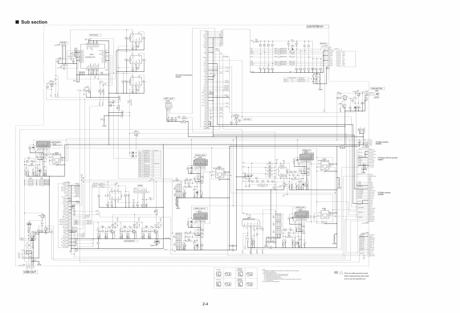
2-4
Sub section
DTA114EKA-X
DTC114EKA-X
A5V REG
ND3.3V
2.UNLESS OTHERWISE SPECIFIED.
3.NI STANDS FOR NOT MOUNTED PARTS.
47k
ALL RESISTORS ARE 1/10W +5% METAL GRAZE RESISTOR.
RT1P141C
10k
10k
F --- FILM CAPACITOR
NOTES
CONDITION --- DVD MODE
ALL CAPACITANCE VALUES ARE IN uF(p=pF)
RT1P441C
ALL CAPACITORS ARE 50V,25V,16V CERAMIC CAPACITOR.
RT1N441C
RT1N141C
1.VOLTAGES ARE DC-MEASURED WITH A DIGITAL VOLT METER WITHOUT INPUT SIGNAL.
10k
ALL RESISTANCE VALUES ARE IN OHM.
ALL E.CAPACITORS ARE SHOWN IN THE FORM OF CAPACITANCE(uF)/RATED VOLTAGE(V).
47k
UN2111-X
47k
UN2211-X
47k
10k
9.1V
1.6
V0V
0.9
V
5.3
V
14
.2V
2.5
V
1.0
V
0V
1.6V
5.0V
2.5V
5.0V
NCB31HK-102X
KW-NX7000 E/EE
R6223
C6210
NRSA63J-0R0X
A_
3.3
V
0V
0V
5.8V
5.1V
5.2
V
5.1
V
5.1
V
0V
5.1
V
5.1
V
0V
0V
3.0V
0V
5.0V
0V
1.6V
3.0V
1.0
V
1.8
V0V
0.9
V
8.1
V
14
.2V
2.5
V
0V
5.2
V0V
3.5
V
3.0
V
3.2V
0V
1.6V
2.5V
5.0V
1.0
V
5.2
V
14
.2V
0.9
V
2.5
V
1.5
V0V
1.3
V
1.0
V
14
.2V 0
V
2.5
V
3.4
V
1.0
V
0V
5.1
V
1.7
V
14
.0V
0V
5.3V
0V
0V
0V
0V
0.2V
0V
0.8V
0V
0.2V
0.8V0.8V
0.2V
0V
3.2
V
0V
3.2
V2
.5V0
V
5.0
V
3.2V
3.2V2.8V
0V
2.8
V
2.9
V0V
3.2
V3
.2V
2.8
V
0V
0V
2.9
V
1.5
V
0V
2.5
V
2.8
V 0V
0V
2.1
V
0V
2.1
V
0V
2.8
V
0V
1.5
V
2.8V
0V
2.8V
3.2V
0V
1.5V
0V
0V
0V
0.8
V0V
0V
0V
2.8
V0V
1.5
V
0V
0V
2.8V
2.8V
0V
0V
0V
2.8V
0V
1.5V
0V
0.1V
3.2V3.2V
C6607
EMCKW-NX7000 J
NI
NI
LVA10799-A1
KW-NX7000 JKW-NX7000 E/EE
NI
NI
NI
NI
NI
NI
NI
NI
NI
NI
NI
NI
NI
NI
NI
NAL0066-001X
NQL79GM-470X
NQL79GM-470X
QETN1HM-106Z
QETN1HM-106Z
NI
NCB31HK-103X
NCB31HK-104X
NCB31HK-103X
NRSA63J-103X
NRSA63J-0R0X
NRSA63J-0R0X
NRSA63J-0R0X
NRSA63J-101X
NRSA63J-101X
NRSA63J-101X
AD7920BKS-X
CN652
L6603
L6601
C6606
C6605
C6604
C6602
R6641
R6639
R6638
R6637
R6620
R6619
R6618
IC654
1%
1%
1%
1%
1%
1%
1%
1%
NAVI RGB BUF.
GPS Module
GYRO
DD
D SG
D
OPT_OUT
ND5V
NA5V
GYRO
GPS ANT
SWREG_5V
DGND
4 S3.3V
7
3
CLK
2
9
DATA1
5
DATA3
SD SLOT
DATA2
8
DGND
1
6
CMD
DATA0
SWREG_ND5V
SWREG_ND3.3VSWREG_M8V
5.2
V
1.0
V
1.5
V
1.0
V
2.5
V
2.5V
0V
5.0V 1.6V
3.2V
0V14.2V
0V0V14.2V
14.2V
1%
USB OUT
RT
EN
/SY
NC
SW
VIN
FB
GN
D
INV
0V
USB POWER
MFAN MOTOR
QAR0353-001
TO FAN
M681
FAN MOTOR
D_GND
D_GND
D_
3.3
V
DATA0
DATA1
DATA2
DATA3
NAVI-VGND
D4V
M8V
S5V
M5V
D5V
D2V
AD
_IN
0
USB_D+
USB_D-
FA
NC
ON
T
SD
_IN
M8V
SD_IN
FANCONT
PANEL5V
PA
NE
L5
V
HMI-PWR
NAVI-VGND
P_GND
HSYNC
VSYNC
NA
VI_
B
NA
VI_
G
NA
VI_
R
GYRO_DATA
GPS_RST
GPS_RST
B
AD
_IN
1
VGND
P_
GN
D
R G B
VG_GND
GYRO_CLK
GYRO_CS
GYRO_DATA
ANT
AD_IN1
AD_IN0
G
R
GPS_RX
GPS_TX
D_3.3V
NAVI_RST
GP
S_
RX
GP
S_
TX
AN
T
HSYNC
VSYNC
NAVI_B
NAVI_R
MSW1
XD_UCS
XD_SCS
XD_SCLK
XD_U2SDT
XD_S2UDT
XD_CPURST
DAC4OUT
MSW4
FR-CH
FL-CH
XD_LRMUTE
HM
I-P
WR
NAVI_RST
NAVI_SI
NAVI_SO
NAVI_SCK
NAVI_RDY
NAVI_REQ
MAIN_REQ
VG_OUT
NAVI_G
GYRO_CLK
GYRO_CS
VG_GND
D_GND
32.768KHZ
VG_OUT
NAVI_SI
NAVI_SO
NAVI_SCK
NAVI_RDY
NAVI_REQ
MAIN_REQ
32.768KHZ
D_GND
VGND
DAC4OUT
FR-CH
FL-CH
MSW4
MSW1
XD_CPURST
XD_S2UDT
XD_U2SDT
XD_SCLK
XD_SCS
XD_UCS
XD_LRMUTE
D2V
D5V
USB_D-
S5V
D4V
M5V
USB_D+
CMD
CLK
WP
CD
S3.3V
DATA2
DATA3
CMD
S3.3V
CLK
DATA0
DATA1
CD
WP
SGND
SGND
SGND
SGND
SGND
SGND
SGND
SGND
SGND
sure to use the specified one.
When replacing those parts make
Parts are safety assurance parts.!
!
!
!
!
!
NQL79GM-220X
L6201
NQR0022-002XK6208
NQR0022-002XK6207
NQR0022-002XK6209
NQR0022-002XK6206
NQR0022-002XK6205
NQR0022-002XK6204
NQR0022-002XK6203
180R6219
180R6218
180R6217
100R6216
180R6215
680
R6141
1.2
k
R6
14
0
C6
12
0
NI
2SC3928A/QR/-XQ6107
R6
50
7
33
k
R6
50
61
2k
R6
50
1
12
k
R6
50
2
33
k
NI
R6
51
4N
IR
65
13
TP614
EN
/SY
NC
7
INV
6
FB
5
GN
D
4
RT
3
SW
2
VIN
1
BD9781HFP-WIC605
EN
/SY
NC
7
INV
6
FB
5
GN
D
4
RT
3
SW
2
VIN
1
BD9781HFP-WIC603
EN
/SY
NC
7
INV
6
FB
5
GN
D
4
RT
3
SW
2
VIN
1
BD9781HFP-WIC652
EN
/SY
NC
7
INV
6
FB
5
GN
D
4
RT
3
SW
2
VIN
1
BD9781HFP-WIC651
C6
61
8N
I
NI
R6
62
4
CS
6
DA
TA
5
CL
K
4
VIN
3
GN
D
2
VD
D
1
*IC
65
4
NI
C6
12
6
NI
C6
12
5
NI
C6
12
4
NI
C6
12
3
NI
R6614
NI
R6621
NI
R6616
MA
111-X
D6
20
3
MA
111-X
D6
20
4
C6
23
21
/16
C6
23
01
/16
C6228
1/16
C6
23
11
/16
C6
22
91
/16
C6226
1/16
C6224
1/16
C6
22
71
/16
C6225
1/16
C62221/16
C6223
1/16
C6221
1/16
C6220
1/16
NI
R6
12
0N
IC
61
22
NI
R6
10
6
NI
C6
12
1
NI
C6
51
6
NI
C6
51
7
0
R6643
0
R6646
0
R6648
ISA
15
30
AC
1/Q
R/X
Q6
60
2
NI
R6
64
2
NI
R6
64
4
NI
R6
64
7
C6
62
0N
I
C6
62
1N
I
NI
L6607
NI
L6606
C6
61
9N
I
C6
61
6N
I
NI
L6605
C6
61
7N
I
C6
62
21
/16
C6
01
4
47
0/2
5
NI
R6
64
9
0.1
C6
61
5
NIR6144
1.5
R6118
1.5
R6115
1.5
R6114
1.5
R6113
1.5
R6119
1.5
R6112
1/16C6725
NI
R6
14
2
NIR6143
SL601
100
R6715
1/1
6C
62
19
NIC6012
NI
C6011
NIC6013
NIC6218
NI
C6
21
7
TP663
5678
43211
50
RA
65
4
5678
43211
50
RA
65
3
QZ
W0
01
0-0
01
PP
60
2
R6191
NI
5678
4321
15
0R
A6
05
5678
4321
15
0R
A6
04
5678
4321
15
0R
A6
03
5678
4321
15
0R
A6
52
5678
43211
50
RA
65
1
NI
R6
64
0
*
R6
64
1
QZ
W0
01
0-0
01
PP
60
1
TP605
TP610
TP611 TP612
TP613
TP609
TP658
TP660
TP655
TP657
TP606
TP604
TP603
TP602
TP601
TP664
TP607
TP653
TP662 TP661 TP659
TP666
TP651
TP608
4
3 2
1
NQ
R0
53
6-0
01
X
L6
00
1
5
6
7
8
4
3
2
1150
RA601
5
6
7
8
4
3
2
1150
RA602
22
R6
70
2
NI
R6
22
6
10
k
R6
70
3
NIR6003
R6
01
2
56
k
NI
R6210
NI
R6
211
R6008
3k
*R6637
*R6638
*R6639
R6
01
3
82
k
R6009
39k
47
k
R6
20
5
3.3
k
R6
21
2
1%
R6
00
61
0k
10k
R6705
39
0
R6
00
7
0
R6
011
R6
10
8
33
k
0
R6
13
9
NI
R6
13
8
NIR6135
R6
10
9
82
k
R6
10
71
2k
NI
R6132
0
R6
13
3
R6110
3.3k
10
k
R6
22
1
NI
R6
20
8
R6111
NI
47
k
R6
20
6
NI
R6
00
5
NI
R6010
R6
10
3
82
k
R6
10
11
2k
R6
22
8
0
R6
10
2
33
k
180R6213
33
k
R6
01
8
2.2k
R6707
5.6
k
R6
22
2
NI
R6
20
9
47
k
R6
20
7
100kR6709
100kR6710
100kR6708
0R6220
NI
R6
22
4
10kR6124
47
k
R6
20
4
R6105
3.3k
NI
R6
01
7
R6104
NI
*
R6
22
3
R6001NI
R6002NI
NI
R6
60
4
R6
50
3
82
k
NI
R6
01
6
100
R6611
NI
R6
01
9
NI
R6
02
0
0R
66
03
NIR6004
0R
66
08
R6504
5.6k
100
R6607
2.2
k
R6
60
6
2.2
k
R6
61
0
0R
66
12
27
kR
67
12
4.7kR6711
100
R6601
R6202
22
2.2
k
R6
61
5
R6
20
3
47
0
100
R6602
R6201
22
R6505 NI
100
R6617
R6512
47k
R6511
22k
R6116
82k
R6117
47k
R6510
NI
4.7
k
R6
22
5
180
R6214
R6
50
8
82
k
*R6618
*R6619
*R6620
30
0R
66
05
30
0R
66
09
30
0R
66
13
R6227
2.2
R6509
2k
RT1N141C-XQ6203
RT1N141C-X
Q6106
NIQ6001
NIQ6002
RT1P141C-XQ6501
RT1P141C-XQ6202
ISA
15
30
AC
1/Q
R/X
Q6
60
3
ISA
15
30
AC
1/Q
R/X
Q6
60
1
S
G
D
RTR020P02-XQ6701
2SD1994A/RS/-TQ6201
2SD2704K-XQ6704
NQLC8CM-470X
L6501
NQLC8CM-470X
L6102
NQLC8CM-470X
L6101
NQLC8CM-470X
L6002
NQLC8CM-470X
L6502
NQL79GM-220X
L6103
NQL79GM-220X
L6106
NQL79GM-220X
L6503
*
L6601
NQL79GM-220X
L6105
NQL79GM-220X
L6107
*L
66
03
NQ
L7
9G
M-2
20
X
L6
60
2
NI
L6108
NQ
L7
9G
M-2
20
X
L6
70
1
6.2
n
L6
70
5
NQ
R0
20
1-0
05
X
L6
70
2
NQ
R0
20
1-0
05
X
L6
70
3
0.039
L6704
NQR0022-002XK6202
0
K6201
NQ
R0
02
2-0
05
X
K6
70
1
NQR0022-005X
K6210
NQR0022-005X
K6211
7654321
BD9781HFP-WIC601
6 5 4
321
RS
Q0
25
P0
3-W
Q6
10
5
NC
5
VO
UT
4
GN
D
3
VIN
2
ON
/OF
F
1
NJM2886DL3-35-XIC607
54 3
21
NIIC604
54 3
21
TC7SET08FU-J-XIC653 5
4 32
1
TC7SET08FU-J-XIC606
54 3
21
TC7SET08FU-J-XIC602
VO
UT
5 4
ON
/OF
F
3
GN
D
2
VIN
1
S-1
112
B2
JM
C-W
IC6
56
VO
UT
5 4
ON
/OF
F
3
GN
D
2
VIN
1
S-1
11
2B
15
MC
-WIC
65
8
VO
UT
5 4
ON
/OF
F
3
GN
D
2
VIN
1
S-1
11
2B
2JM
C-W
IC6
57
GN
D
1
VC
C
2
VIN
3
TOTX177L
IC608
NI
D6
00
5
MA
81
20
/M/-
X
D6
20
1
NID6001NID6002
MA111-X
D6505
MA
22
D2
3-X
D6
10
1
MA111-X
D6202
RB
05
1L
-40
-X
D6
10
2
MA
22
D2
3-X
D6
50
1
MA
22
D2
3-X
D6
50
3
RB
05
1L
-40
-X
D6
50
2
RB
05
1L
-40
-X
D6
10
4
MA
22
D2
3-X
D6
10
3
MA
22
D2
3-X
D6
00
3
MA
22
D2
3-X
D6
00
4
MA111-X
D6506
RB
05
1L
-40
-X
D6
50
4
NQR0436-001X
C6723
NQ
R0
43
6-0
01
XC
67
22
T4
7/2
5
C6
20
7
*C6
60
7
47/25
C6702
47/16
C6701
10
/50
C6
21
2
*C6
60
5
C6
00
31
0/5
0
15
0/6
.3C
65
09
15
0/6
.3C
65
03
47
/25
C6
10
5
10
/50
C6
111
10
/50
C6
10
3
15
0/6
.3C
60
01
47
/25
C6
10
9
NI
C6
11
6
C6
21
3
10
/50
C6
21
4
10
/50
C6
10
20
.1
0.0
01
C6
00
9
0.1
C6
118
2.2
/10
C6
117
C6
10
1
0.0
04
7
0.1
C6
51
5
C6
10
40
.01
NI
C6
20
2
C6107 0.01
0.1
C6
11
9
C6
70
5
12
p
0.3
3
C6
115
NI
C6
60
8
C6
50
1
10
/25
C6
50
5
0.0
04
7
0.0047
C6704
C6
11
3
0.0
04
7
C6
110
0.0
1
C6114 0.01
C6
50
4
0.1
*
C6
60
2
C6513
0.01
C6
112
0.1
*
C6
21
0
C6
50
8
10
/25
C6
511
0.0
04
7
C6
51
2
0.1
0.1
C6
01
0
C6
00
41
/50
C6
211
NI
0.0
01
C6
00
5
C6
21
6
0.0
1
0.1
C6
10
8
*
C6
60
4
C6
00
20
.01
C6
00
6
0.1
C6
00
7
0.0
04
7
C6
71
32
.2/1
0
*
C6
60
6
C6
71
24
70
p
C67112.2/10
0.0047
C6703
2.2
/10
C6
71
8
2.2
/10
C6
71
4
2.2
/10
C6
72
0
1/1
6
C6
72
1
1/1
6
C6
71
9
0.1
C6
51
4
1/1
6
C6
71
7
C6710
4p
NI
C6
70
6
NI
C6
70
7
NI
C6
70
8
2.2
/10
C6
71
5
0.01C6609
C6008 0.01
2.2/10C6716
0.1
C6
51
00
.1C
65
06
0.1
C6
10
6
0.1
C6
20
8
NI
C6
20
1
0.0
01
C6
20
6
0.0
01
C6
20
5
0.1
C6
61
3
C6
21
5
0.0
1
NI
C6
20
4
0.1
C6
61
4
NI
C6
20
3
NI
C6
20
9
GND4
GND3
14.4V2
14.4V1
QGA2501F1-04CN607
NAVI_PWR14
GPS_RST13
U3.3V12
VG_OUT11
VG_GND10
NAVI_RST9
NAVI_SI8
NAVI_SO7
NAVI_SCK6
NAVI_RDY5
NAVI_REQ4
MAIN_REQ3
DGND2
32.768kHz1
QGF0523F2-14WCN653
USB_DET30
USB_FUNC29
FANCONT28
SW_FREQ27
VDD5V26
HMI_PWR25
USB_PWR24
DVD_SW23
XD_LRMUTE22
A9V21
FL-CH20
AGND19
FR-CH18
AGND17
XD_UCS16
XD_SCS15
XD_SCLK14
XD_U2SDT13
XD_S2UDT12
XD_CPURST11
DGND10
DAC4OUT9
VGND8
MSW47
MSW16
NC5
NC4
NC3
SPEED PULSE2
SD_IN1
QGF0534F3-30XCN605
36353433
EDO32
GND31
RFIN30
GND29
VLNA28
VRF27
GND26
VBB25
nW
AK
EU
P
24
GN
D
23
VD
DR
TC
22
TIM
ER
SY
NC
21
GN
D
20
RX
B
19
GN
D
18
TX
B
17
RFPWRUP 16
GND 15
TIMEMARK 14
RXA 13
TXA 12
ECLK 11
GND 10
SCLK 9
VD
DR
EG
8
GN
D
7
RT
C_
OU
T
6
ON
_O
FF
5
GN
D
4
nS
RE
SE
T
3
GN
D
2
SK
1
NAU0005-001X
IC659
WP 60
CD 59
DATA1 58
DATA0 57
DGND 56
CLK 55
S3.3V 54
CMD 53
DATA3 52
DATA2 51
DGND 50
D+ 49
D- 48
DGND 47
D5V 46
C 45
LRMUTE 44
SW 43
A9V 42
RL-CH 41
AGND 40
RR-CH 39
A5V 38
FL-CH 37
AGND 36
FR-CH 35
D2V 34
D2V 33
DGND 32
TX 31
DGND 30
UCS 29
SCS 28
SACK 27
SCLK 26
U2SDT 25
S2UDT 24
CPURST 23
DAC5_OUT 22
DGND 21
DAC4_OUT 20
VGND 19
DAC1_OUT 18
DGND 17
DAC2_OUT 16
SW4 15
DAC3_OUT 14
SW1 13
S5V 12
D4V 11
D4V 10
M5V 9
M5V 8
M8V 7
M8V 6
M8V 5
MGND 4
MGND 3
MGND 2
MGND 1
QGF0534F3-60XCN602
NAVI_R 40
NAVI-VGND 39
NAVI_G 38
NAVI-VGND 37
NAVI_B 36
NAVI-VGND 35
AD_IN0 34
AD_IN1 33
ANT 32
DGND 31
DGND 30
ND5V 29
ND3.3V 28
ND3.3V 27
GYRO_CLK,GA5 26
GYRO_CS,GS 25
GYRO_DAAT,GG 24
SPEED_PULSE 23
GPS_TX 22
GPS_RX 21
VSYNC 20
DGND 19
HSYNC 18
DGND 17
PCK 16
DGND 15
NA5V 14
VG_OUT 13
VG_GND 12
DGND 11
DGND 10
/NAVI_RST 9
TX 8
RX 7
SCK 6
/NAVI_RDY 5
/NAVI_REQ 4
/MAIN_REQ 3
DGND 2
32.768kHz 1
QGB0812L2-40XCN651
WP12
CD10
COMMON11
DATA18
DATA07
DGND6
CLK5
S3.3V4
DGND3
CMD2
DATA31
DATA29
14
13
NNZ0202-001XCN603
NAVI-B12
NAVI-VGND11
NAVI-G10
NAVI-VGND9
NAVI-R8
NAVI-VGND7
VSYNC6
PANEL5V5
HSYNC4
D_3.3V3
P-GND2
A_3.3V1
QGB1004K2-12WCN606
NC
8
VT
7
VO
UT
6
NC
5
NC
4
VD
D3
GN
D2
NC
1
*CN652
FG
1
GN
D2
D+
3
D-
4
VB
US
5
QGA2001F1-05CN601
312QAM0953-001CN654
1
2
QGA2001F1-02CN604
CN908To Main section
CN801To Panel 2/Front section
WR981To Main section
CN401To Front end section
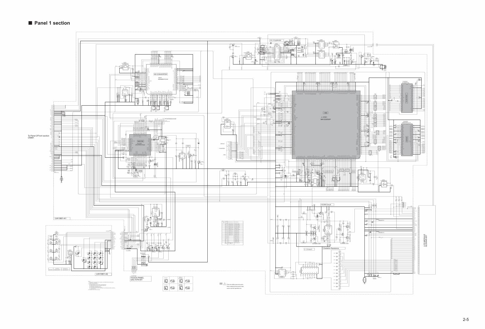
2-5
Panel 1 section
5.2
V 0V
3.2
V
SMLE12WBC7W-XNECBB205/WPQR/X
KW-NX7000 J KW-NX7000 E/EE
D552-D563
LVA10801-A2
VC
C
VOL +
OPEN
GN
D
POWER
po
we
r
OU
T
DISPMAP
VOL -
RST
QAL1078-001TOUCH PANEL
LC
D M
OD
ULE
QL
D0
54
5-0
01
UN2111-X
47k
ALL RESISTORS ARE 1/10W +5% METAL GRAZE RESISTOR. RT1P141C
10k
10k
F --- FILM CAPACITOR
NOTES
CONDITION --- DVD MODE
RT1N141C
1.VOLTAGES ARE DC-MEASURED WITH A DIGITAL VOLT METER WITHOUT INPUT SIGNAL.
10k
DTA114EKA-X
2.UNLESS OTHERWISE SPECIFIED.
DTC114EKA-X
ALL CAPACITANCE VALUES ARE IN uF(p=pF)
RT1P441C
3.NI STANDS FOR NOT MOUNTED PARTS.
ALL CAPACITORS ARE 50V,25V,16V CERAMIC CAPACITOR.
47k
RT1N441C UN2211-X
47k
10k
ALL RESISTANCE VALUES ARE IN OHM.
ALL E.CAPACITORS ARE SHOWN IN THE FORM OF CAPACITANCE(uF)/RATED VOLTAGE(V).
47k
NI
B409
B408
NRSA63J-0R0XNI
NRSA63J-0R0X
0V
3.2
V
0V
0V
3.3
V
0V
3.2
V
0V
0V
0V
0V
3.2
V
0V
-.-V
0V
0V
3.2V
3.3V
-.-V
0V
0V
3.2V
3.2V
2.5V
3.2V
0V
3.2V
0V
0V
0V
0V
0V
0V
0V
3.3V
0V
3.2
V
1.9
V 0V
1.9
V
1.9
V 0V
3.2
V
1.9
V0V
0V
3.2
V
3.3
V
3.3V
0V
3.2V
3.2V
0V
0V
3.2V
0V
0.5V
0V
0.6
V
3.2
V
3.3
V
12.9V
4.9V
5.1V
0V
2.6V
0.7V
5.1
V 0V
1.6
V
1.7
V1
8.9
V
18
.9V
18
.9V
18
.9V
3.3V
0V 3.3V
0V
0V
3.3V
0V
2.6V
0V
3.3V
3.3V0V
5.1V5.2V
4.5V
3.2V
0V
0V
5.1V
0.1V0V
0.1V
3.3V
1.9V
2.7V
2.7V
1.5V
1.4V
0V
2.6V
2.6V
5.1V
0V
1.6V
1.9V
1.3V
2.6V
0.4V
3.4V
5.1V
5.1V
3.2V
7.1V
7.1V
7.1V
7.0V
7.0V
7.1V
7.0V
7.0V
12.4V
14.1V
14.1V
0V
12.4V
2.5V
0V
2.5V
0V0V
0V
0V
0V
0V
0V
0V
0V
0V
0V
0V
1.6V
1.6V
3.2V
3.2V
0V
0V
1.6V
1.6V
5.2
V
1.6
V
2.6
V
2.6
V
1.6
V
1.6
V
2.6
V
1.6
V
2.6
V
2.6
V
1.6
V
1.6
V 0V
2.6
V
8.5V
1.7V
2.2V
1.7V
-5.1V
1.1V
2.2V
-5.2V
1.7V
1.1V
8.6V
1.7V
0.3V
1.4V
0V
1.7
V
-5.2
V
0.7
V
0.6
V
8.6
V
4.0
V
1.4
V
1.4
V
-12.0V
-5.2V
-5.8V
18.8V
8.6V
9.2V
0V
2.5V
1.8V
0V
0V
3.2V
3.2V
3.2V
0V
3.2V
0V
0V
0V
2.0V
0V
1.3V
0V
0V
3.2V
1.4V
3.2V
0V
0V
3.2V
1.3V
0V
0V
2.0V
0.2V
0V
0V
0V
0V
0V
1.3V
1.4V
0V
2.0V
1.3V
0V
1.4V
0V
1.5V
3.2V
1.6V
0V
1.4V
3.1V
3.2V
3.2V
3.2V
0V
0V
3.2V
0V
0.6V
0V
3.1V
2.0V
0.5V
3.2V
0V
0V
0V
1.4V
3.2V
0V
1.6V
1.5V
0.7V
0.1V
0.9V
1.0V
0.9V
1.4V
3.2V
0.1V
1.3V
1.8V
2.2V
1.0V
0.4V
1.0V
1.6V
2.7V
3.2V
0V
2.2V
1.0V
0V
0.4V
1.3V
0.1V
1.9V
1.0V
0V
0.5V
1.6V
0V
0.1V
0V
0V
3.2V
3.2V
0V
0V
0.5V
0.5V
0.1V
0V
0.5V
2.7V
2.7V
2.7V
2.7V
0.4
V
1.0
V
1.3
V
1.6
V
3.0
V
2.2
V
3.2
V
1.3
V
1.6
V
0.1
V
1.0
V
0.4
V
1.0
V
0.1
V
1.9
V
1.0
V
2.2
V
1.8
V
0V
3.2
V
1.5
V
1.0
V
0.1
V
3.2
V
0.9
V
0.7
V
0V
0.9
V
1.4
V
0V
1.6
V
0.1
V
0.1
V
0.5
V
0V
0V
0V
0.5
V
2.7
V
0.5
V
3.2
V
0V
2.7
V
0V
0V
2.7
V
1.6
V
0V
2.7
V
0.5
V
0V
3.2
V
2.7
V
0V
1.3V
1.5V
1.6V
1.0V
1.5V
0V
3.2V
1.5V
1.1V
0V
0V
0V
3.2V
3.2V
3.1V
3.2V
3.1V
0V
0V
0V
0V
0V
0V
1.6V
0V
2.0V
0V
0V
0V
0.7V
0V
0V
0V
1.3V
1.4V
1.4V
0V
3.2V
3.2V
1.6V
2.0V
2.0V
0.2V
0.6V
1.3V
0.1V
1.4V
0V
2.0V
2.0V
3.2V
1.4V
0.5V
0.4V
0V
0.4
V
0.1
V 0V
0.5
V
0.4
V
0.7
V
0.7
V
0.7
V
1.6
V0V
0V
0.7
V
0.7
V
1.6
V
1.6
V
3.2
V
3.2
V
1.5
V
0.6
V
0.1
V
0.9
V
0.8
V0V
0.9
V
3.2
V
1.6
V
0.7
V0V
3.2
V
1.5
V
3.2
V0V
1.4
V
1.5
V
3.2
V 0V
1.3
V 0V
0V
0V
1.9
V
1.5
V
0.9
V
1.3
V
3.2
V
3.2
V
1.5
V
1.6
V0V
1.3
V 0V
1.6
V
1.6
V
3.2V
0V
3.3V
0V
3.2V
1.4V
1.6V
3.2V
3.2V
3.2V
3.3V
3.2V
3.2V
0V
3.2V
3.2V
3.2V
0V
3.2V
1.6V
3.2V
3.2V
1.6V
3.2V
3.2V
3.2V
3.2V
0V
1.6V
KW-NX7000 E/EE KW-NX7000 J
NRSA6AJ-0R0W NRSA6AJ-2R2W
(SDRAM)K4S641632K-UC75OR
M12L64164A-7TG
NRSA63J-0R0X
K4S641632K-UC75
NI
IC511
NDC31HJ-101XNI
NDC31HJ-101XNI
NDC31HJ-101XNI
NBE40JM-107XNBE40JM-476X
NCBA1AK-104W NCJA0JK-105W-R
REF
MODEL
B405
C4635
C4734
C4733
NCB31AK-105XC5308 NCB31HK-471X
C5307
C5304
NCB31CK-104X
C5303
C5302
NCB31AK-105X
C5039
NCB31AK-105XNCB31HK-471X
C5027
C5003
C5002
NCB31AK-105XNCB31CK-104X
C5001
R5004
NCB31AK-105XNCB31HK-471X
NCJA0JK-105W-RNCBA1AK-104W
NCJA0JK-105W-RNCBA1AK-104W
NCJA0JK-105W-RNDCA1HJ-471W
3.0V
3.2V
3.0V
3.0V
0V
LVA10801-A1
1.6
V
3.2
V
1.6
V0
V
1.6
V
3.2
V
3.0V
3.2V
1.7V
1.7V
0V
3.2V
0.3V
1.8V
0.4V
0.2V
0.4V
0.1V
0.3V
1.7V
0.1V
1.8V
1.7V
1.8V
0V
0.3V
3.2V
1.7V
0.1V
1.8V
0.3V
LED-B-4-2
LED-B-3
LED-B-4-1
POWERLED
3.2V
HMI
AD CONVERTER
MICON
PROGRAM&DEBUGGER
DWire32
A0
RY/BY
Q1
A6
GND
OE
Q0
BYTE
Q15/A-1
WE
A19
A9
A8
A17
Q11
A20
Q6
Q13
Q5
A15
WP
A10
RESET
A14
GNDA3
A5
CE
A4
Q7
A18
A11
A7
A1
A13
Q4
A12
Q14
Q8
Q2
Q9
Q12
Q10
Q3
A16
A2
VCC
A21
3.2V
0V 0V
SD
RA
M
0.5
%0
.5%
0.5
%0
.5%
0.5
%0
.5%
0.5
%0
.5%
0.5
%0
.5%
0.5
%0
.5%
0.5
%
JTAG
F-KAKIKOMI
2Y
3A2A
3Y
1A
GND
VCC
1Y
RS
T
VD
DN
C
GN
D
RESET
3.2V
2.8V
1.6V
0V
3.3V
1.7V
3.2V
0V
0V
0.9V
0V
0V
0V
0.3V
3.2V
0.3V1.8V
3.2V
0.2
V0V
0.2
V
0.2
V
3.2
V
3.2
V0V
0V
0.4
V 0V
3.2
V 0V
2.6
V
1.9
V
0.4
V
0.9V
1.9
V
0V
1.6
V
2.0V
1.4
V
3.0V
1.7
V
2.0V
3.2
V
3.3V
1.6
V
3.2V
0.4
V
1.6V
1.6
V
0V
1.6
V
1.8V
1.6
V
1.8V
0.2
V
1.8V
0.1
V
0V
2.9
V
1.8
V
1.3
V
0.3
V
1.8
V
0.7
V
0.3
V
0V 0
.4V
1.8
V
3.2
V
1.8
V
0V
1.7V
0V
1.7V
0V
0V
1.3V
3.2
V
3.0V
3.2
V
1.7V
0V
0.1V
1.7V
0V
U3.3V
Gradation Rasistance
VCOM Circuit
CFL CTL&DRIVER
D1
DIM
NDRD
G2
ENA
LCT
D2
G1
S2
D1
PDRA
NDRB
CT
D1
VDDA
G1
CTIMR
S1
RT1
CMP
REFD1
D2FB
D2
GNDAPGND
SST
PDRC G2
LPWM
D2
OVP
RT
S1
S2
FLA
SH
RO
M
D3
.3V
V-RST
FRST
DISPCLK
NA
VI-
R
NA
VI-
G
NA
VI-
B
KE
Y2
KE
Y1
D8
D7
D6
D5
D4
D3
D2
D1
A5
A4
A3
A2
A1
A0
WE
CS
D1
5
D1
4
D1
3
D1
2
D11
D1
0
D9
FO
E
A6
A7
A8
A9
A1
0
A11
A1
2
A1
3
A1
4
A1
5
A1
6
A1
7
A1
8
A1
9
A2
0
CL
K
SDDATA12
SDDATA13
SDDATA14
SDDATA15
SDAD8
SDAD9
SDAD11
SDAD12
IR2
IR3
IR4
IR5
KEY2
KEY1
SCL
SDA
A3.3V
HD
COMAC
COMDC
HMI-RST
HMI-RST
SD
A
SC
L
COMPOSITE
TP
KE
Y2
TP
KE
Y1
LED-B-4-1
LED-B-3
LED-B-4-2
RESETSW
REMOCON
KEYIN1
KEYIN2
FRST
LED-ON
DIMMER
M-LED
M-SENSE
B2
B1
B0
G0
G1
R2
OZ
_P
WR
OZ
_P
WR
R1
R0
CF
L-C
TL
G5
G4
G3
G2
G1
G0
R2
R0
R1
R3
R4
R5
BL
-ON
VIN
HIN
DVCLK
B0
B1
B2
B3
B4
B5
VIN
HIN
DVCLK
R3
R4
R5
G2
G3
G4
G5
B3
B4
B5
SDAD12
IR3
IR5
HOUT
IB0
IB1
IB2
IB3
IB4
IB5
IG0
IG1
IG2
IG3
IG4
IG5
IR0
IR1
IR2
IR4
CSY
KEYDATA
DISPCLK
DISPCE
DISPDATA
NAVI-R
NAVI-G
NAVI-B
VD
HD
SDDATA4
SDDATA11
SDDATA10
SDDATA9
SDDATA8
VD
HD
DIMMER
LED-ONBL-ON
CFL-CTL
CO
MD
C
KEYDATA
DISPDATA
CE
DE
N
VO
UT
DE
N
VO
UT
CE
SUBRST
BL
-DIM
TP
X1
TP
Y1
TP
X2
TP
Y2
M-SENSE
M-LED
KE
YIN
2
KE
YIN
1
BL-DIM
VD
V-RST
TP
Y2
TP
KE
Y2
TP
X2
TP
KE
Y1
TP
Y1
TP
X1
COMAC
SDDATA0
CS
Y
DISPCE
SUBRST
FOE
A16A15
A2
1
D0
SDAD4
SDAD5
SDAD6
SDAD7
SDAD8
SDAD9
SDAD11
SDCKE
SDM1
SDDATA8
SDDATA9
SDDATA10
SDDATA11
SDDATA12
SDDATA13
SDDATA14
SDDATA15
SDAD3
SDAD2
SDAD1
SDAD0
SDAD10
SDBA1
SDBA0
SDCS
SDRAS
SDCAS
SDWE
SDM0
SDDATA7
SDDATA6
SDDATA5
SDDATA4
SDDATA3
SDDATA2
SDDATA1
SDDATA0
SDDATA1
SDDATA2
SDDATA3
SDDATA5
SDDATA6
SDDATA7
SDM0
SDWE
SDCAS
SDRAS
SDCS
SDAD10
SDBA0
SDBA1
SDAD0
SDAD3
SDAD1
SDAD2
SDAD4
SDAD5
SDAD6
SDAD7
SDCKE
SDM1
IR1
CL
K
IG4
D14
IG3
IG2
IG1
IG0
A12
CS
D11
IB5
A13
IB4
IB3
D7
D13
IB2
A14
A1
IB1
A18
D8
IB0
A6
D6
D12A20
A11
A19
D9
D0
A2
A4
A5
A17
D4
D15
A8
WE
HO
UT
A10
A3
D2
A0
D5
A9
IR0
D1
D3
A21
D10
A7
IG5
GND
sure to use the specified one.
When replacing those parts make
Parts are safety assurance parts.!
!
!
!
!
*D
55
8
C568
NI
C5
54
NI
C5
62
NI
*D
56
1
C5
57
NI
3.9
kR
55
6
*D
56
2
R5
58
47
k
NSW0312-001XS558
NSW0312-001XS551
C5
58
NI
321
RS-771-XIC551
*D
55
4
C5
52
0.1
/10
C5
53
0.0
01
*D
55
9*
D5
57
*D
55
6
C5
65
NI
NSW0312-001XS552
C5
66
NI
C567
NI
3k
R5
51
TP561
C551
NI
NSW0312-001XS553
NSW0312-001XS555
NSW0312-001XS559
C5
59
NI
*D
55
5
C569
NI
C5
61
NI
*D
56
0
2.7
kR
55
4
C5
56
NI
NSW0312-001XS557
C5
64
NI
*D
56
3
CL
-20
1IR
-X-X
D5
51
R557
0
*D
55
3
3.9
kR
55
5
C5
60
NI
NSW0312-001XS556
3k
R5
52
C5
63
NI
C5
55
NI
NSW0312-001XS554
*
D5
52
2.7
k
R5
53
4321
60
59
58
57
56
55
54
53
52
51
50
49
48
47
46
45
44
43
42
41
40
39
38
37
36
35
34
33
32
31
30
29
28
27
26
25
24
23
22
21
20
19
18
17
16
15
14
13
12
11
10
9
8
7
6
5
4
3
2
1
2
1
B411
0
0.1
C5
06
5
100
R5115
65
432
1
TC7PA14FU-XIC504
NI
R4725
NI
R4724
NI
R4726
MA8062/M/-XD4303
NID4002
MA8120/M/-XD508
MA8120/M/-XD509
NIC5064
T
C4
73
5
0.1
/10
0.0
01
C4
38
0.0
01
C4
37
*B405
*
B408
8
7
6
5
1
2
3
4
68RA501
8
7
6
5
1
2
3
4
68RA503
*
B409
NIC5063
NIC5062
NI
C5
06
1
NI
C5
06
0
C436 NI
R4
63
1N
I
D4611
NI
NQL382M-220XL5004
NQL52EM-100XL4602
NQ
L3
82
M-4
70
XL
46
01
NQ
L3
82
M-4
70
X
L4
30
2
NQ
L3
82
M-4
70
X
L4
30
1
NQL79GM-220X
L4002
NQL79GM-220X
L4001
C4635*
22R4756
NIC5
15
NIC5
16
NI
C4
35
NI
C4
34
NQ
R0
45
0-0
01
XC
50
59
C4734 *
C4733 *
10K
R5114
10K
R5113
NIC5058MA2SD31-X
D5002
MA2SD31-XD5001
47/6.3C5315
T
MA
111-X
D5
07
MA
111-X
D5
06
0.0
01
C5
14
0.0
01
C5
13
10
0p
C5
12
10
0p
C5
11
10
0p
C5
10
10
0p
C5
09
10
/6.3
C5
05
6
10
/6.3
C5
05
7
10/6.3
C5055
10/6.3
C5314
10/6.3
C5313 10/6.3
C5312
0.001
C5049
0.0
01
C5
08
0.0
01
C4
73
2
0.0
01
C4
73
10.001
C507
543
21
IC473TC7SH08FU-X
0
R4763
NI
C5053
NI
C5054
R5
08
8N
I
R4
57 0
R4
56 0
10K
R5036
NI
R5
03
5
0
R5034
0R
45
5
NIC5052
C417NI
C416NI
NI
C4
15
NI
C4
14
NI
C433NI
C432
NI
C5311
NI
R5033
NI
D4
61
0
NI
D4
60
9
0.1C5051
R4
63
0
NI
NI
R5104
+-
+-
+-
+-
NA
X0
97
0-0
01
XX
50
02
9.6
MH
z
TP494
TP519
TP521
TP
46
4
TP414
TP520
TP402
TP466
TP434
TP
46
7
TP468
TP
46
9
TP470
TP471TP473
TP474
TP502
TP412
TP476
TP478
TP479
TP417
TP437
TP501
TP407
TP431
TP435
TP409
TP401
TP411
TP410
TP518
TP408
TP413
TP
48
1
TP436
TP416
TP404
TP415
TP
52
2
TP523
TP480
2
3
4
5
6
10
NQR0636-001T4601
5678
43213
3R
A5
20
8
7
6
5
1
2
3
4
68RA506
5
6
7
8
4
3
2
1
68RA509
8
7
6
5
1
2
3
4
68RA508
8
7
6
5
1
2
3
4
68RA507
8
7
6
5
1
2
3
468
RA505
8
7
6
5
1
2
3
4
68
RA504
8
7
6
5
1
2
3
4
68RA502
5678
43213
3R
A5
21
5
6
7
8
4
3
2
1
33RA522
47
0
R5
06
2
220
R5102
22kR529
22kR527
R46050
R5
110
NI
R5
11
2
NI
22kR5028
0R5204
NIR424
47
kR
47
08
NIR4712
NIR4710
NIR4709
1k
R4
70
6
1k
R4
70
5
1k
R4
70
4
R4615 47
220
R5101
R5
21
NI
R4608
0
R46065.1M
R520
68k
R519
68k
R4
52
47
k
R4609 33k
R5
24
1.8
K
R5
25
NI
R5
23
4.7
k
0R
50
64
R5
22
10
k
R4604 100k
R4
01
2
10
k
10
k
R5
07
8
68
R4
73
1
68
R4
72
8
68
R4
72
9
68
R4
73
0
R4613270k
NI
R5304
NI
R4
76
5
33
R5
00
9
NI
R4
76
4
0R
50
76
NI
R5
07
5
10
0R
40
5
100R5024
100R5023
0R
50
79
NI
R4
76
6
R4
02
5N
I
R4
62
7
47
k
47
0
R5
06
3
R4004
68k
R4363 0
R4
20
5
39
7.5
kR
50
59
R4364 0
R4
01
61
5k
R4
20
3
82
R4
62
9
5.6
k
R4017
10k
R4
20
6
43
0R5030
6.2
k
R5
06
0
2.7
k
R5
06
1
R4625
NI
R4
20
7
47
R4624
NI
12
kR
50
57
R4
62
3
NI
R4023
27k
R4
62
2
NI
0R
50
65
R4
61
7
5.1
k
0R5206
0R5207
0R5208
0R5209
0R5210
0R5211
1.5
k
R5
10
6
1k
R5
20
1
1k
R5
20
2
0
R4
76
7
68
0R
50
68
R4014
22k
R4002
68k
R4
01
0
NI
NI
R5001
R4001
68k
NI
R436
R4
20
2
22
0
0R5008
R4
03
3
2.2
R4
03
0
10
k
0R5002
NI
R5
00
3
22
R5
08
5
NI
R5
07
3
R4109
NI
*R5
00
4
100R4748
100R4749
R4308 0
R4307
0
R4
30
3
0
R4
30
5
0
R4
30
1
0
68R5005
R4
02
0
10
k
68R5006
R4614 47
R4018
10k
R4626
51k
R4
02
6
10
k
68R5007
10
0R
42
8
R4
02
9
10
k
R4365 0
10
0R
43
5
100R437
1kR416
R4
51
2.2
k
100R419
1k
R4
29
R4
011
10
k
R4009NI
1kR414
100R418
R4
02
8
10
0
R4003
68k
1k
R4
33
R4
61
6
5.1
k
1k
R4
30
R4
50
33
k
1kR422
R4110
0
R4
00
8
10
0k
1k
R4
11
0R423
33
R5
02
2
1k
R4
01
R4
00
5
10
0k
33
R5
10
0
1k
R4
31
NIR415
R4
61
81
M
0R440
10
k
R5
011
R4108
0
10
0R
40
3
33
R5
09
9
1k
R4
32
100R413
1kR439
R461147
R454470k
1k
R4
02
100R442
B4
03
NI
10
0R
42
5
1k
R4
07
R4
20
4
47
1kR438
NIR445
1k
R4
10
R4
53
47
k
100R441
B4
02
NI
10
0R
42
7
10
0R
40
4
10kR443
B4
01
NI
NIR444
R4
48
47
0k
10
0R
41
2
33
R5
09
8
R4603220k
10
0R
43
4
1k
R4
08
R4
20
1
24
1kR421
R4
60
16
.8k
15
kR
44
6
R44947k
0
R4
20
R4
03
2
2.2
10
0R
42
6
R4
03
4
39
1k
R4
09
R461282k
R461047
R4
03
1
39
1kR417
15
kR
44
7
1k
R4
06
R4
21
0
20
0
R4607
180k
R4
62
1
39
0
R4358 0
R4
61
9N
I
R4
20
8
68
R4
62
0
0
10kR5010
R4
211
10
1kR4754
R4366 0
68
R4
74
1
R4359 0
68
R4
73
2
R4
02
1
10
k
R4367 0
68
R4
74
2
R4107
NI
68R4720
68
R4
73
3
R4
01
9
10
k
R4360 0
R4
01
3
10
k
R4
01
5
10
k
100R4751
33p
R4703
NI
R5012
33
R5
09
7
R5
30
2
10
k
33p
R4702
R4
02
2
10
k
68R4719
68R4723
R4361 0
0R4713
R4368 0
R4362 0
33p
R4701
0R4707
R4
21
2
10
100R4714
R4035
10
R4
20
9
16
0
0R5050
0R
50
82
100R4715
R4
02
4
3.9
k
68R4722
0R5049
1k
R4
75
9
R4
02
7
10
k
R5105
390
68
R4
73
8
68
R4
74
3
68R4721
33
R5
09
2
0R4716
0R5043
68R4718
0R5044
0R5048
0R5037
68
R4
73
9
68R4717
100R5025
1.5k
R4755
0R5038
0R4752
68
R4
74
0
3.3
k
R5
26
3.3
k
R5
28
22
k
R5
33
3.3
k
R5
36
47
0k
R5
35
3.3
k
R5
32
47
0k
R5
31
22
k
R5
37
1kR5031
100R5020
2.2
k
R5
30
100R5021
R517
47
100R5026
33
R5
08
7
22R5032
100R5017
2.2
k
R5
34
100R5018
100R5027
100R5029
0R
50
83
0R
50
84
47
0
R5
10
3
100
R5019
R518
100
100R5013
100R5016
100R5015
100R5014
NI
R5
06
7
10
k
R5
06
6
0R
50
58
10
k
R5
07
2
0R
50
69
0R
50
70
0R
50
71
0R
50
80
NI
R5107
0R
50
77
0R
50
74
10
0R
50
86
0R
50
81
UN2211-XQ4607
UN2211-XQ507
UN2211-XQ403
NIQ5002
S
G
D
NIQ4603
S
G
D
NI
Q4
60
4
S
G
D NIQ4601
2S
D601A
/QR
/-X
Q4003
2S
C5
93
8A
/B/-
XQ
511
2S
D601A
/QR
/-X
Q402
2SD601A/QR/-XQ506
2S
D601A
/QR
/-X
Q4004
2S
D601A
/QR
/-X
Q4007
2S
D601A
/QR
/-X
Q4001
NIQ4602
2S
C5
93
8A
/B/-
XQ
51
0
ISA
1530A
C1/Q
R/X
Q4006
ISA1530AC1/QR/XQ4605
ISA1530AC1/QR/XQ4005
ISA1530AC1/QR/XQ401
ISA1530AC1/QR/XQ4002
2S
A2
11
9K
-XQ
50
8
2S
A2
11
9K
-XQ
50
9
ISA
15
30
AC
1/Q
R/X
Q5
00
1
NQ
L3
82
M-2
20
XL
47
02
NQL382M-220X
L5001
NQL382M-100XL401
NQL085J-470XL5005
0K
50
1
0K
50
4
0K
50
3
0K
50
2
21
6L
CD
_R
_1
21
5L
CD
_R
_0
21
4L
CD
_G
_5
21
3L
CD
_G
_4
21
2V
SS
211
VD
D3
21
0L
CD
_G
_3
20
9L
CD
_G
_2
20
8L
CD
_G
_1
20
7L
CD
_G
_0
20
6L
CD
_B
_5
20
5L
CD
_B
_4
20
4L
CD
_B
_3
20
3L
CD
_B
_2
20
2L
CD
_B
_1
20
1L
CD
_B
_0
20
0L
CD
ICL
K
19
9V
DD
19
8V
SS
19
7V
DD
3
19
6L
CD
CL
K
19
5L
CD
VS
Y
19
4L
CD
HS
Y
19
3L
CD
DE
N
19
2L
CD
CS
Y
19
1L
CD
CE
19
0N
C
18
9N
C
18
8L
CD
MU
TE
18
7M
CK
SL
18
6V
DD
3
18
5V
SS
18
4V
DD
18
3T
ST
C0
18
2T
ST
C1
18
1T
ST
CK
18
0O
SC
XO
17
9O
SC
XI
17
8P
MO
DE
0
17
7A
VC
LK
17
6T
ST
IO
17
5A
VD
DB
17
4D
AO
UT
17
3A
VS
SB
17
2C
LL
17
1C
LH
17
0A
VS
SA
16
9A
INP
1
16
8A
INP
0
16
7A
VD
DA
16
6V
RE
FL
16
5V
RE
FH
16
4V
CM
O
16
3IR
EF
16
2
DVVSY
16
1
DVHSY
16
0
DVCLK
15
9
DVR_0
15
8
DVR_1
15
7
VDD3
15
6
VSS
15
5
DVR_2
15
4
DVR_3
15
3
DVR_4
15
2
DVR_5
15
1
DVG_0
15
0
DVG_1
14
9
DVG_2
14
8
DVG_3
14
7
DVG_4
14
6
DVG_5
14
5
VDD3
14
4
VSS
14
3
DVB_0
14
2
DVB_1
14
1
DVB_2
14
0
DVB_3
13
9
DVB_4
13
8
DVB_5
13
7
DISP_CLK
13
6
INTR
13
5
XRST
13
4
VDD3
13
3
VSS
13
2
VDD
13
1
KEY_DATA
13
0
DISP_DATA
12
9
VCOMAC_PWM
12
8
F_DATAO
12
7
F_DATAI
12
6
SDA
12
5
SCL
12
4
DPSEL
12
3
SDATA
12
2
SCLOCK
12
1
VDD3
12
0
VSS
11
9
V_RESET
11
8
F_RESET
11
7
SUB_RESET
11
6
DISP_CE
11
5
RON
11
4
VDDP_2
11
3
VDDP_1
11
2
VDDP_0
111
VOUT_2
11
0
VOUT_1
10
9
VOUT_0
10
8V
SS
10
7F
DA
TA
_0
10
6F
DA
TA
_1
10
5F
DA
TA
_2
10
4F
DA
TA
_3
10
3F
DA
TA
_4
10
2V
SS
10
1V
DD
3
10
0F
DA
TA
_5
99
FD
ATA
_6
98
FD
ATA
_7
97
FD
ATA
_8
96
FD
ATA
_9
95
FD
ATA
_1
0
94
FD
ATA
_11
93
FD
ATA
_1
2
92
FD
ATA
_1
3
91
FD
ATA
_1
4
90
VD
D
89
VS
S
88
VD
D3
87
FD
ATA
_1
5
86
FR
OE
85
FR
CS
84
FR
WE
83
FA
D_
0
82
FA
D_
1
81
FA
D_
2
80
FA
D_
3
79
FA
D_
4
78
FA
D_
5
77
VD
D
76
VS
S
75
VD
D3
74
FA
D_
6
73
FA
D_
7
72
FA
D_
8
71
FA
D_
9
70
FA
D_
10
69
FA
D_
11
68
FA
D_
12
67
FA
D_
13
66
FA
D_
14
65
FA
D_
15
64
FA
D_
16
63
FA
D_
17
62
VD
D3
61
VS
S
60
FA
D_
18
59
FA
D_
19
58
FA
D_
20
57
FA
D_
21
56
FA
D_
22
55
VS
S
54SDDATA_0
53SDDATA_1
52SDDATA_2
51SDDATA_3
50SDDATA_4
49VSS
48VDD3
47SDDATA_5
46SDDATA_6
45SDDATA_7
44SDM_0
43SDWE
42SDCAS
41SDRAS
40SDCS
39SDAD_10
38SDBA_0
37VDD
36VSS
35VDD3
34SDBA_1
33SDAD_0
32SDAD_1
31SDAD_2
30SDAD_3
29SDAD_4
28SDAD_5
27SDAD_6
26SDAD_7
25SDAD_8
24SDAD_9
23VDD3
22VSS
21VDD
20SDAD_11
19SDAD_12
18MIMCLK
17MEMCLK
16SDCKE
15SDM_1
14SDDATA_8
13SDDATA_9
12SDDATA_10
11SDDATA_11
10SDDATA_12
9VDD3
8VSS
7SDDATA_13
6SDADTA_14
5SDDATA_15
4LCD_R_5
3LCD_R_4
2LCD_R_3
1LCD_R_2
MN103SE60P
IC501
GND80
PVD 1.8V79
FILTER78
GND77
PVD 1.8V76
GND75
PVD 1.8V74
C-CLAMP73
EXTCLK/COAST72
V-SYNC071
H-SYNC070
V-SYNC169
H-SYNC168
SCL67
SDA66
GND65
VDD 3.3V64
BLUE063
BLUE162
BLUE261
BL
UE
3
60
BL
UE
4
59
BL
UE
5
58
BL
UE
6
57
BL
UE
7
56
BL
UE
8
55
BL
UE
9
54
GN
D
53
VD
D 3
.3V
52
GR
EE
N0
51
GR
EE
N1
50
GR
EE
N2
49
GR
EE
N3
48
GR
EE
N4
47
GR
EE
N5
46
GR
EE
N6
45
GR
EE
N7
44
GR
EE
N8
43
GR
EE
N9
42
DA
VD
D 1
.8V
41
GND 40
GND 39
VDD 3.3V 38
RED0 37
RED1 36
RED2 35
RED3 34
RED4 33
RED5 32
RED6 31
RED7 30
RED8 29
RED9 28
GND 27
VDD 3.3V 26
DATACLK 25
SOG-OUT 24
HS-OUT 23
VS-OUT 22
O/EFIELD 21
RE
FH
I
20
RE
FC
M
19
RE
FL
O
18
PW
R-D
N C
TL
17
R-A
IN1
16
GN
D
15
R-A
IN0
14
VD
3.3
V
13
SO
G-I
N1
12
GN
D
11
G-A
IN1
10
VD
3.3
V
9
SO
G-I
N0
8
GN
D
7
G-A
IN0
6
VD
3.3
V
5
B-A
IN1
4
GN
D
3
B-A
IN0
2
VD
3.3
V
1
AD9980KSTZ-80
IC471
VSS 54
DQ15 53
VDD1
DQ02
VDDQ3
DQ14
DQ25
VSSQ6
DQ37
DQ48
VDDQ9
DQ510
DQ611
VSSQ12
DQ713
VDD14
LDQM15
WE16
CAS17
RAS18
CS19
BA020
BA121
A10/AP22
A023
A124
A225
A326
VSSQ 52
DQ14 51
DQ13 50
VDDQ 49
DQ12 48
DQ11 47
VSSQ 46
DQ10 45
DQ9 44
VDDQ 43
DQ8 42
VSS 41
N.C/RFU 40
UDQM 39
CLK 38
CKE 37
A12 36
A11 35
A9 34
A8 33
A7 32
A6 31
A5 30
A4 29
VSS 28VDD27
K4S641632K-UC75IC511
VDD 48
VSS 47
REGC 46
X1 45
X2 44
FLMDO 43
NC 42
NC 41
SUB_RST 40
KEY_LED 39
KEY_DIM 38
NC 37
TP
_IN
T
36
CF
L-G
AT
E2
35
NC
34
SU
B_
RE
Q
33
NC
32
NC
31
NC
30
NC
29
TP
_K
EY
2(Y
)
28
TP
_K
EY
1(X
)
27
KE
Y2
26
KE
Y1
25
AVSS24
AVREF23
BL_ON22
CFL_GATE21
SELF20
TXD619
RXD618
M_SENSE17
M_LED16
VCOMDC_PWM15
KEY_INT14
OCD1A13
OC
D1
B
12T
PY
211
TP
X2
10
TP
Y1
9
TP
X1
8
BL
_D
IM2
7
BL
_D
IM
6
NC
5
NC
4
NC
3
SD
A
2
SC
L
1
UPD78F0515GAIC451
12
34
56
78
91
011
12
13
14
15
16
17
18
19
20
21
22
23
24
25
26
27
28
29
30
31
32
33
34
35
36
37
38
39
40
41
42
43
44
45
46
47
48
IC512SG32N90TFI03
12
34
56
78
91
0
11
12
13
14
15
16
17
18
19
20
OZ964ISN-XIC461
1A
1
1Y
2
2A
3
2Y
4
3A
5
3Y
6
GN
D
7
VC
C
14
6A
13
6Y
12
5A
11
5Y
10
4A
9
4Y
8
TC
74V
HC
T04A
FT
-XIC
411
1 2 3 4
5678
NJM
072B
V-X
IC402
1 2 3 4
5678
NJM
2904V
-X
IC513
12
34 5
67
8
TC7W04FK-XIC412
12
34 5
67
8
TPCP8402JVC-XIC463
12
34 5
67
8
TPCP8402JVC-XIC464
GN
D
6
XO
UT
5
CO
NT
4
XIN
3
VD
D
2
F_
OU
T
1
NJU
6368P
F1-X
IC502
543
21
TC7SH04FU-XIC503
VIN
5
VO
UT
4
NC
3
GN
D
2
ST
BY
1
IC472NJM2878F3-18-X
543
21
TC7SET08FU-J-XIC462
43
2 1
S-8
0824C
NN
B-G
-WIC
452
4 3
21
10.0MHzNAX0974-001XX401
43 2
1
16
.5M
Hz
NA
X0
97
1-0
01
XX
50
01
3 21
MC
2836-X
D402
BAV99L-XD4604
BA
V99L-X
D4607
MA8047/M/-XD4606
MA8047/M/-XD4603
MA8047/M/-XD4602
MA
8047/M
/-X
D4605
NI
D5
04
MA2SD31-XD4302
NI
D5
05
NI
D5
03
MA2SD31-XD4301
D4601
MA111-X
D4608NI
NI
D5
02
MA
111-X
D4
01
MA2SD32-XD4001
NQ
R0
45
0-0
01
XC
43
02
NQR0450-001XC4601
NQ
R0
45
0-0
01
X
C4
30
1
T
C4
70
12
2/6
.3
*
C5
02
7
T
47/6.3
C402 T
22/6.3
C5309
T
T
47
/6.3
C4
30
8
TC4
72
7
22
/6.3
22
/6.3
C5
02
9
T
NI
C5306
T
T
47
/10
C4
30
7
0.1
/10
C5
02
2
C4715 0.1/10
C4
70
90
.1/1
0
C4
00
3
0.4
7/1
0
C4
00
4
0.4
7/1
0
C4720 1/16
0.0
47
/16
C4
05
C4
01
7
0.1
/10
C4
31
01
0/2
5
C4
72
6
0.1
/10
C4
01
4
NI
10
0p
C4
03
C4303
0.1/16
C4085p
C4
13
0.0
47
/10
0.0
47
/10
C4
06
C4305
0.1/10
10
0p
C4
04
C47180.1/10
C4
01
50
.1/1
6
C411
0.01/16
C4
70
70
.1/1
0
C4101/6.3
C401 1/6.3
C4
00
9
0.1
/16
C4
12
4.7
/6.3
C4090.47/10
C4101
0.1/16
C4016
10/16
C4
72
8
NI
C4075p
C4
70
40
.1/1
0
C5
04
0
10
p
C5
04
1
10
p
C4306
0.1/10
0.1/10C5042
C4
71
00
.1/1
0
C4102
0.1/16
C4
72
90
.1/1
0
C5
04
30
.1/1
0
C47230.082/16
C4
70
80
.1/1
0
C4
70
20
.1/1
0
C471210/6.3
C4
00
6
10
/25
C4
01
3
0.1
/10
*
C5307
*
C5308
10
/16
C4
311
0.1/10
C5301
*
C5302
*
C5303
*
C5304
C4
00
8
1/1
6
0.1/10
C5305
C4
00
2
0.4
7/1
0
C4
70
60
.1/1
0
C4
70
50
.1/1
0
C4
71
3
10
/6.3
C4634
NI
C4
63
3
NI
C4
711
0.1
/10
C4
70
30
.1/1
0
C47250.1/10
*C5001
*
C5002
C4
30
91
0/2
5
*C5003
0.1/10
C5005
C4
00
1
0.4
7/1
0
C47220.1/10
C4304
0.1/50
0.1/10
C5004
0.1/10C5006
0.1
/10
C5
00
7
C4
01
2
1/1
6
C4
01
0
10
/16
0.1
/10
C5
00
8
0.1
/10
C5
00
9
C4
71
70
.1/1
0
0.1
/10
C5
01
0
0.1
/10
C5
011
0.1
/10
C5
01
2
10
/6.3
C4
73
0
*
C5
03
9
C4
71
60
.1/1
0
C4719 1/16
C46190.047
C4607 0.47/10
C46180.047
C5
02
0.1
/50
C4
62
51
0/2
5
C4
62
41
0/2
5
C4614100p
C4609100p
C47210.1/10
C5
03
0.4
7/1
0
C5
04
0.4
7/1
0
C462710/25C4608
0.1/10
C4611
0.047
C4
62
31
0/2
5
C4714 0.1/10
C47240.0082
C50510/25
22/6.3C5044
4.7/6.3
C501
0.1/10C5017
C4
62
2
1/5
0
0.1/10C5019
0.1/10C5018
C46030.1/10
0.1/10C5020
0.1
/10
C5
05
0
C462610/25
C4616100p
C4610
0.1/10
0.1/10C5021
C4615220pC4606 0.01/16
C4
62
90
.04
7
68
pC
50
48
18
p
C5
04
7
NIC5046
C5
06
NI
0.1
/10
C5
04
5
0.1
/10
C5
03
80.1
/10
C5
03
7
0.1
/10
C5
03
6
0.1
/10
C5
03
5
C4617100p
0.0
1/1
6C
50
32
33
p
C5
03
1
68
p
C5
03
0
C422 0
C421 NI
C4
62
1
1/5
0
C4612
NI
C4
62
01
0/2
5
C4613100p
C423 NI
C463122p/3k
0.1
/10
C5
02
5
C46052.2/10
C4628
2.2/16
C46021/6.3
C4
63
00
.03
3
C4
26
NI
0.1
/10
C5
02
4
C4604 NI
C4
63
20
.00
39
C5
03
31
0p
C4
27
NI
0.1
/10
C5
02
8
C4
29 0
0.1
/10
C5
02
6
C4
28
0
C5310
0.1/1010/6.3C5015
C4
31
0
10/6.3C5016
10/6.3C5013
0.1/10C5014
C4
30
0
C5
03
41
0p
0.1
/10
C5
02
3
S.GND16
M-LED15
LED18.5V14
KEY113
KEYIN112
LED-B-311
LEDB-4-210
LEDGND9
DGND8
POWERLED7
LEDB-4-16
KEYIN25
KEY24
RESETSW3
REMOCON2
ACC5V1
QGF0545F3-16XCN551
CFL+B 1
CFL+B 2
CFL+B 3
CFL+B 4
CFL-F-CTL 5
INVGND 6
INVGND 7
INVGND 8
INVGND 9
DGND 10
U3.3V 11
SUB-REQ 12
SUB_RST 13
DISPDATA 14
DISPCE 15
DGND 16
DISPCLK 17
DGND 18
KEYDATA 19
HMI-RST 20
ACC5V 21
REMOCON 22
RESETSW 23
DGND 24
PANEL5V 25
PANEL5V 26
PANEL5V 27
D3.3V 28
D3.3V 29
AD3.3V 30
-12V 31
-12V 32
18.5V 33
18.5V 34
LED18.5V 35
LED18.5V 36
LEDGND 37
LEDGND 38
LED-B-4-2 39
LED-B-3 40
LED-B-4-1 41
POWERLED 42
LED-ON 43
DIMMER 44
DGND 45
VGND 46
COMPOSITE 47
VGND 48
VGND 49
HD 50
DGND 51
VD 52
DGND 53
A3.3V 54
NAVI-VGND 55
NAVI-R 56
NAVI-VGND 57
NAVI-G 58
NAVI-VGND 59
NAVI-B 60
QGF0534F3-60XCN503
RE
SE
T9
PS
28
FL
MD
O7
TX
6
RX
5
VD
D4
VS
S3
OC
D1
A2
OC
D1
B1
QGF0522F3-09WCN404
GND60
STH159
V058
V157
V256
V355
V454
V553
V652
V751
V850
V949
V1048
DA047
DA146
DA245
DA344
DA443
DA542
DB041
DB140
DB239
DB338
DB437
DB536
DC035
DC134
DC233
DC332
DC431
DC530
LOAD29
L/R28
NC27
VDD2/5V26
VDD2/5V25
VDD2/5V24
NC23
GND22
GND21
CPH20
GND19
NC18
VDD1/3.3V17
VDD1/3.3V16
STH215
NC14
VGH/18.5V13
NC12
GND11
STV210
OE9
CPV8
U/D7
STV16
NC5
VGL/-12V4
NC3
VCOM2
VCOM1
QGF0534F2-60XCN401
S.GND 1
M-LED 2
LED18.5V 3
KEY1 4
KEYIN1 5
LED-B-3 6
LEDB-4-2 7
LEDGND 8
DGND 9
POWERLED 10
LEDB-4-1 11
KEYIN2 12
KEY2 13
RESETSW 14
REMOCON 15
ACC5V 16
QG
F0
52
3F
2-1
6W
CN
50
1
EXTRG 15
3.3V 14
SCLCLK 13
SDATA 12
INTR_LOW 11
FDTA_I 10
FDTA_O 9
RESET 8
GND 7
TRCD2 6
TRCD3 5
TRCD0 4
TRCD1 3
TRCCLK 2
TRCST 1
QGF0522F3-15WCN504
y-t
op
1
x-r
igh
t2
y-b
ott
om
3
x-le
ft4
QG
F1
03
9F
2-0
4X
CN
50
2
2
1
QGA8002F1-02XCN403
CN881To Panel 2/Front section

2-6
Panel 2/Front section
0V
0V0V
0V
17.7
V
18.4V
18.3V
18.4V
0V
NRSA63J-392XR8825 NRSA63J-272X
NRSA63J-362XR8824 NRSA63J-182X
NRSA63J-472XR8823 NRSA63J-332X
NIR8822 NRSA63J-332X
NRSA63J-362XR8821 NRSA63J-332X
NRSA63J-392XR8820 NRSA63J-272X
NRSA63J-362XR8819 NRSA63J-182X
NRSA63J-113XR8813 NRSA63J-562X
NRSA63J-113XR8812 NRSA63J-562X
NRSA63J-681XNRSA63J-471X
NX7000J NX7000E/EE
R8811
LVA10800-A1
0V
3.0V
0V
LED-B-4-1
0V
17.6V
POWERLED
LED-B-3
0V
VIDEO
LED-B-4-2
0V
0V
3.0V
0V
0V
0V
15.5V
0V0V
-12.1V-12.1V
0V
0V
0V0V
0V
0V
0V0V
0V
0V
18.4V
18.4V
0V
0V
0V
0V
0V
3.0V0V
0V
18.4
V
13.9
V
CFLPOWER SW
0V
0V
3.0V
3.0V
13.8
V
SD DET
3.0V
5.2
V
3.0
V
5.2
V
3.3V
3.5
V
3.5
V
0V
0V
LVA10800-A2
0V
3.5
V
18.4
V
13.8
V
18.4
V
13.8
V
18.4
V
18.4
V
13.8
V
5.2
V
3.5
V
ADC REG
0.1V
0V0V
5.2
V0V
0.1V
3.5
V
SLOT LED
5.2
V
3.5
V
5.2
V0V
SENSOR
0.2V 0.1V
LVA10800-A3
0V0V0V
DOOR MOTOR
PHOTO
1.2V
M
0V
QAR0378-001
47k
10k
F --- FILM CAPACITOR
RT1N441C
RT1P441C UN2111-X
1.VOLTAGES ARE DC-MEASURED WITH A DIGITAL VOLT METER WITHOUT INPUT SIGNAL.
10k47k
ALL CAPACITANCE VALUES ARE IN uF(p=pF)
47k
10k ALL CAPACITORS ARE 50V,25V,16V CERAMIC CAPACITOR.
ALL RESISTANCE VALUES ARE IN OHM.
RT1P141C
DTC114EKA-X
RT1N141C
10k
ALL RESISTORS ARE 1/10W +5% METAL GRAZE RESISTOR.
2.UNLESS OTHERWISE SPECIFIED.
CONDITION --- DVD MODE
47k
ALL E.CAPACITORS ARE SHOWN IN THE FORM OF CAPACITANCE(uF)/RATED VOLTAGE(V).
3.NI STANDS FOR NOT MOUNTED PARTS.DTA114EKA-X
NOTESUN2211-X
CFL-F-CTL
RESETSW
RESETSW
DISPDATA
A3.3V
HMI-RST
G
DIMMER
KEYDATA
R
HMI-RST
LED-ON
VD
HD
DISPCE
B
DISPDATA
SUB_RST
DISPCLK
SUB-REQ
SUB_RST
R
CFL-F-CTL
G
REMOCON
A3.3V
B
DISPCLK
REMOCON
DISPCE
SUB-REQ
VD
KEYDATA
HD
ACC5V
DETACH
DISPCE
NAVI-G
NAVI-B
SUB-REQ
DISPCLK
ACC5V
RESETSW
CFL-F-CTL
REMOCON
NAVI-B
DISPCE
DISPDATA
NAVI-R
HMI-RST
DETACH
SUBRST
KEYDATA
DETACHSW
RESETSW
REMOCON
HD
VIDEO
VD
VD
A3.3V
VIDEO
SUB-REQ
SUBRST
NAVI-G
DETACHSW
KEYDATA
A3.3V
HD
HMI-RST
DISPDATA
DISPCLK
NAVI-R
CFL-F-CTL
SGND
S.GND
NI
C8811
NI
D8841
MA
8051/M
/-X
D8826
MA
8051/M
/-X
D8824
NID8802
R8814
NI
NI
C8804
MA
8150/M
/-X
D8829
R8819
*
NI
R8835
MA
8062/M
/-X
D8836
NI
D8805
R8813
*
NI
C8803
MA
8200/M
/-X
D8830
R8815
47k
NI
R8834
MA
8051/M
/-X
D8835
NI
D8804
R8821
*
MA
8051/M
/-X
D8821
MA
8051/M
/-X
D8812
NI
C8802
NI
R8806
NI
R8833
MA
8051/M
/-X
D8834
MA
8051/M
/-X
D8820
NI
D8806
UN
22
11
-XQ
8805
R8812
*
NI
C8801
UN
22
11
-XQ
8803
NI
R8832
MA
8051/M
/-X
D8833
NIC8810
MA
8051/M
/-X
D8819
NID8809
R8822
*
NI
D8839
R8824
*
MA
8051/M
/-X
D8813
UN
2111
-XQ
8801
MA
8051/M
/-X
D8832
0R8803
NI
R8831
R8818
5.6
k
MA
8051/M
/-X
D8818
NI
D8840
R8811
*
NI
D8814
ISA1530AC1/QR/X
Q8804
MA
8200/M
/-X
D8811
0R8802
MA
111
-X
D8810
MA
8051/M
/-X
D8831
NI
C8808
NI
D8825
21
NS
W0225-0
01X
S8801
NI
D8837
MA
8051/M
/-X
D8815
ISA1530AC1/QR/XQ8802
0
R8801
R8816
5.6
k
NID8803 N
IC
8807
MA
8051/M
/-X
D8828
2.2
k
R8805
NI
D8838
MA
8051/M
/-X
D8816
R8817
47k
R8820
*
TP8810
NI
D8807
MA
8051/M
/-X
D8827
R8825
*
MC
2838-X
D8801
MA
8051/M
/-X
D8823
R8823
*
MA
8051/M
/-X
D8817
NI
D8808
NI
R8836
MA
8051/M
/-X
D8822
C8014
NI
C8011
2.2
/10
NI
D8038
NI
C8007
R8017
0
NI
R8007
NI
C8013
NI
C8012
R8046
6.8
kR
8047
6.8
k
TP803
D
6
D
5
S
4
G
3
D
2
D
1
RS
Q025P
03-W
Q8017
C8005
0.3
3/1
0
R8010
NI
MA
8051/M
/-X
D8019
MA
8051/M
/-X
D8020
MA
8051/M
/-X
D8028
MA
8051/M
/-X
D8024
NI
D8025
C8008
NI
LS
Q971/K
L/-
X
D8004
MA
111
-X
D8006
C8002
NI
NI
R8039
0.0
1
C8010
NI
R8044
0
R8042
NIQ8016
C8006
10/2
5
R8006
NI
MA
8062/M
/-X
D8036
R8034
6.8
k
33k
R8003
R8035
NI
MA
8200/M
/-X
D8011
D
6
D
5
S
4
G
3
D
2
D
1
NI
Q8013
0R8511
R8008
NI
NI
Q8007
R8011
NI
R8016
NI
R8032
6.8
k
C8001
NI
R8029
10k
TP806
MA
8051/M
/-X
D8034
MA
8051/M
/-X
D8026
0R
8038
MA
8051/M
/-X
D8030
R8015
0
TP801
UN2211-XQ8005
R8021
10k
R8013
NI
CL-2
01IR
-XT
S-X
D8007
R8009
NI
MA
8200/M
/-X
D8037
MA
8051/M
/-X
D8027
C8003
10/2
5
NIQ8003
MA
8051/M
/-X
D8015
MA
8051/M
/-X
D8013
2S
D601A
/QR
/-X
Q8002
NQL52EM-220X
L8001
C8004
10/2
5
R8019
0
10k
R8002
D
6D
5
S
4
G
3
D
2
D
1
RS
Q025P
03-W
Q8015
MA
8051/M
/-X
D8018
NI
R8045
NC
5
VO
UT
4
GN
D
3
VIN
2
ON
/OF
F
1
NJM2886DL3-35-XIC801
MA
8051/M
/-X
D8023
MA
8051/M
/-X
D8012
D8003
33k
R8004
NI
F8001
MA
8150/M
/-X
D8035
0
R8041
R8012
NI
MA
8051/M
/-X
D8022
R8022
NI
33KR8001
R8030
6.8
k
R8014
NI
Q80122SD601A/QR/-X
MA
8051/M
/-X
D8017
MA
8051/M
/-X
D8021
NI
R8043
100
R8005
CP
T-1
84S
-CT
S-X
Q8001
TP804
R8020
NI
D
6
D
5
S
4
G
3
D
2
D
1
NI
Q8014
NI
R8027
MA
8051/M
/-X
D8029
MA
8051/M
/-X
D8033
UN2211-XQ8010
NIQ8009
NI
R8028
MA
8051/M
/-X
D8031
R8037
NI
NI
R8026
R8018
0
NIQ8008
R8031
390
R8023
NI
MA
8051/M
/-X
D8016
R8036
NI
NIQ8004
R8025
10k
MA
8051/M
/-X
D8032
MA
8062/M
/-X
D8014
NIQ8006
R8024
0
TP802
543
21
NIIC802
R8033
NI
R8501
750
R8502
NI
150
R8510
NS
W0126-0
01X
S8502
CLO
SE
33kR8504
NS
W0225-0
01X
S8501
OP
EN
R8507
6.8
k
33k
R8505
2SD601A/QR/-XQ8501
1
2 3
4
CPI-210/BC/-XIC851
R8509
1k
R8508
2.2k
R8503
39k
NI
R8506
ACC5V 24
AD3.3V 23
DGND(NC) 22
DGND(NC) 21
DETACHSW 20
RESETSW 19
REMOCON 18
HMI-RST 17
SUB-REQ 16
DGND 15
18.5V 14
-12V 13
VGND 12
CVBS 11
VGND 10
U3.3V 9
DGND 8
INVGND 7
INVGND 6
CFL-F-CTL 5
CFL+B 4
CFL+B 3
SUB_RST 2
DETOUCH 1
QGZ2204M1-24XCN883
DGND 1
DGND 2
NAVI-B 3
NAVI-VGND 4
NAVI-G 5
NAVI-VGND 6
NAVI-R 7
NAVI-VGND 8
A3.3V 9
P-GND(DGND) 10
NAVI_VD 11
P-GND(DGND) 12
NAVI_HD 13
DGND 14
DISPCLK 15
DGND 16
KEYDATA 17
DISPCE 18
PANEL5V 19
DISPDATA 20
D3.3V 21
D3.3V 22
LEDGND 23
LED18.5V 24
QGZ2204M1-24XCN882
CFL+B60
CFL+B59
CFL+B58
CFL+B57
CFL-F-CTL56
INVGND55
INVGND54
INVGND53
INVGND52
DGND51
U3.3V50
SUB-REQ49
SUB_RST48
DISPDATA47
DISPCE46
DGND45
DISPCLK44
DGND43
KEYDATA42
HMI-RST41
ACC5V40
REMOCON39
RESETSW38
DGND37
PANEL5V36
PANEL5V35
PANEL5V34
D3.3V33
D3.3V32
AD3.3V31
-12V30
-12V29
18.5V28
18.5V27
LED18.5V26
LED18.5V25
LEDGND24
LEDGND23
LED-B-4-222
LED-B-321
LED-B-4-120
POWERLED19
LED-ON18
DIMMER17
DGND16
VGND15
COMPOSITE14
VGND13
VGND12
HD11
DGND10
VD9
DGND8
A3.3V7
NAVI-VGND6
NAVI-R5
NAVI-VGND4
NAVI-G3
NAVI-VGND2
NAVI-B1
QGF0534F3-60XCN881
NAVI-B 12
NAVI-VGND 11
NAVI-G 10
NAVI-VGND 9
NAVI-R 8
NAVI-VGND 7
VSYNC 6
PANEL5V 5
HSYNC 4
D_3.3V 3
P-GND 2
A_3.3V 1
QGB1004J2-12XCN801
SD_HLOCK 30
HMI_PWR 29
DETACH 28
RESET_SW 27
REMOCON 26
KEY_DATA 25
DISP_DATA 24
DISP_CE 23
DISP_CLK 22
DETACH_SW 21
SLOT_LED 20
SUB_REQUEST 19
SUB_RESET 18
HMI_RST 17
DGND 16
D10V 15
PANEL-12V 14
LED18.5V 13
PANEL18.5V 12
ACC5V 11
VGND 10
VIDEO 9
DGND 8
CFL_PWR 7
U3.3V 6
CFL14.4V 5
CFL14.4V 4
CFL_F_CNT 3
CFLGND 2
CFLGND 1
QGB1004J2-30XCN802
ACC5V1
AD3.3V2
DGND(NC)3
DGND(NC)4
DETACHSW5
RESETSW6
REMOCON7
HMI-RST8
SUB-REQ9
DGND10
18.5V11
-12V12
VGND13
CVBS14
VGND15
U3.3V16
DGND17
INVGND18
INVGND19
CFL-F-CTL20
CFL+B21
CFL+B22
SUB_RST23
DETOUCH24
QGF0567F1-24WCN804
DGND24
DGND23
NAVI-B22
NAVI-VGND21
NAVI-G20
NAVI-VGND19
NAVI-R18
NAVI-VGND17
A3.3V16
P-GND(DGND)15
NAVI_VD14
P-GND(DGND)13
NAVI_HD12
DGND11
DISPCLK10
DGND9
KEYDATA8
DISPCE7
PANEL5V6
DISPDATA5
D3.3V4
D3.3V3
LEDGND2
LED18.5V1
QGF0567F1-24WCN803
MO
TO
R-
6
MO
TO
R+
5
DG
ND
4
PN
L_S
W3
DG
ND
2
SW
5V
1
QGA1002C1-06XCN851
2 1
QGA1002C1-02XCN852
CN606To Sub section
CN981To Main section
CN503To Panel 1 section
CN961To Main section

2-7
Front end section
LVB10819-A2
0.0V
0.0V
0.0V
0.0V
0.0V
3.2V
0.0V
0.0V
0.0V
0.0V
2.8V
3.2V
2.5V
0.0V
0.0V
0.0V
0.0V
3.2V
0.0V
0.0V
3.2V
3.2V
3.2V
0.0V
1.6V
0.0V
0.0V
4.2V
0.0V
0.0V
3.3V
4.2V
0.0V
2.3V
0.0V
0.0V
2.3V
0.3V0.0V
0.0V
1.2V
0.0V
3.2V
0.1V
0.0V
0.0V
3.2V
0.0V
2.5V
2.5V
2.5V
0.0V
5.0V
5.0V
0.0V
3.2V
1.6V
0.8V
1.5V
0.0V
3.2V
0.0V
0.0V
0.0V
0.0V
0.0V
0.0V
0.0V
0.0V
3.2V
3.2V
0.0V
0.0V
0.0V
2.5V
1.5V
3.2V
3.2V
0.0V
0.0V
3.2V
3.2
V
0.0
V
0.0
V
3.2
V
0.8
V
3.2
V
0.0
V
3.1
V
0.0
V
3.1
V
3.2V
0.0V
0.5V
0.0V
0.0V
0.0V
3.2V
0.0V
0.0V
0.7V
3.2
V
0.0
V
0.0
V
1.1
V
3.2
V
0.0
V
3.1
V
0.0
V
0.0
V
0.0
V
0.6V
0.1V
0.0V
3.2V
0.1V
0.0V
2.6V
0.0V
0.0V
1.7
V
0.1
V
1.1
V
1.1
V
0.0
V
8.0
V
8.0
V
3.2
V
0.0
V
0.0
V
0.0
V
0.0
V
0.0
V
0.0
V
4.0
V
4.0
V
4.0
V
0.9
V
2.9
V
2.9
V
0.0
V
2.9
V
2.9
V
2.9
V
8.0
V
8.0
V
7.4
V
3.7
V
8.0
V
0.0
V
3.2
V
1.6
V
1.6
V
1.6
V
1.6
V
1.6
V
1.6
V
0.0
V
1.6
V
1.6
V
0.0
V
8.0
V
1.7
V
0.6
V
4.9
V
4.9
V
4.9
V
4.9
V
0.0
V
2.5
V
2.4
V
2.5
V
2.4
V
3.7
V
0.0
V
3.3
V
3.3V
3.3V
0.0V
0.0V
4.6V
4.8V
0.0V 3.5V
4.1V
1.9V
1.7V
3.3V
1.1V
4.8V
0.0V
0.0V
0.2V
0.0
V
0.0
V
4.7
V
0.0V
0.0V
4.7
V0
.0V
0.0
V
3.2V
0.0V
0.0V
0.0V
0.0V0.0V
0.0V
0.0V
0.0V0.6V
0.0V
2.5V0.0V
0.0V
0.0V3.2V
0.0V
0.0V
0.0V0.0V
3.2V
3.2V
3.2V
0.0V
0.0V
0.0V
0.0V
3.2V
0.0V
0.0V
2.7V
0.0V
3.2V
3.2V
0.0V
0.0V
0.0V
3.2V
0.0V
0.0V
0.0V
0.0V
0.0V
0.6V
2.5V
0.0V
0.3V
0.0V
0.0V
0.0V
0.0V
0.0V
0.0V
0.0V
0.0V
3.2V
0.0V
0.0V
0.0V
0.0V
0.0V
0.0V
0.0V
0.0V
0.0V
3.2V
0.0V
2.8V
1.3V
0.0V
0.0V
0.0V
0.0V
1.5V
0.0V
3.0V
3.1V
3.1V
3.1V
2.5V
2.6V
2.7V
3.0V
2.9V
2.8V
2.8V
0.0V
2.7V
3.2V
3.2V
0.0V
3.2V
0.0V
3.2V
3.2V
1.5V
1.5V
1.5V
1.4V
0.0V
0.0V
0.0V
1.4V
2.5V
2.7V
2.7V
2.8V
2.8V
2.8V
0.0V
2.6V
2.7V
0.0V
0.0V
3.2V
0.0V
3.2V
0.0V
3.2V
0.0V
0.0V
0.0V
1.6
V
3.2
V
1.5
V0
.0V
1.6
V
3.2
V
1.8
V
1.6
V
3.2
V
0.0
V
1.7
V
3.2
V
3.1
V
3.2
V
0.0
V
0.0
V
1.8
V
1.6
V
1.6
V
0.0
V
0.0
V
3.2
V
0.0
V
3.2
V
0.0
V
3.2
V
0.0
V
3.2
V
3.2
V
1.7
V
0.0
V
0.2
V
1.6
V
0.0
V
0.0
V
0.2
V
0.0
V
1.6
V
1.6
V
1.8
V
1.6
V
1.8
V
1.7
V
3.2
V
2.0
V
2.0
V
0.0
V
0.8
V
0.0
V
2.3
V
1.8
V
0.0
V
0.0
V
3.2
V
0.0
V
0.0
V
1.2
V
0.0
V
0.0
V
1.6
V
0.0V
1.6V
1.6V
0.0V
0.0V
0.1V
0.0V
3.2V
2.2V
1.2V
0.0V
0.0V
0.0V
0.6V
0.1V
0.0V
0.0V
0.8V
1.6V
0.0V
3.2V
1.5V
1.5V
0.0V
1.2V
2.7V
2.7V
2.6V
0.0V
0.0V
0.0V
0.0V
0.0V
0.0V
0.0V
1.5V
1.5V
1.6V
2.2V
1.6V
0.0V
0.0V
2.3V
2.3V
2.3V
2.3V
3.2V
3.2V
3.2V
3.2V
3.1V
1.8V
2.6V
1.6V
D
1.5
V
0.0
V
1.5
V
1.3
V
0.0
V
1.2
V
3.2
V
3.2
V
3.2
V
3.2
V
0.0
V
0.0
V
2.8
V0
.0V
3.2
V
2.8
V
2.8
V
2.8
V
2.9
V
2.8
V
3.0
V0
.0V
3.2
V
2.7
V
2.7
V
2.7
V
2.6
V
2.5
V
2.5
V
0.0
V3
.1V
0.0
V
3.2
V
0.0
V1
.4V
1.2
V
3.1
V
3.1
V
3.0
V
0.0
V
0.0
V
0.0
V
0.0
V0
.0V
3.2
V
1.5
V
0.0
V
0.0
V
1.4
V
0.0
V
1.5
V
0.0
V0
.0V
3.2
V
0.0V
0.0V
0.0V
0.0V
0.0V
0.0V
3.2V
1.2V
0.0V
0.0V
0.0V
0.0V
0.0V
0.0V
0.0V
0.0V
0.0V
3.2V
0.0V
0.0V
3.2V
0.0V
0.0V
0.0V
0.0V
0.0V
0.0V
0.0V
3.2V
0.0V
3.2V
0.0V
0.0V
0.0V
3.2V
0.0V
3.2V
1.2V
3.2V
0.0V
3.2V
0.0V
3.2V
0.0V
3.2V
3.2V
0.0V
0.0V
3.2V
3.2V
0.0V
3.2V
0.1V
3.2V
CH1
CH0
H
LA
CH0
GND
CH1
COM
VCC
A
ADR2
0
ADR1
1
ADR0
0
EEPROM
iPod IC
I2C BUS SLAVE ADDRESS
00 0
SW2 SW3SW1
CE
(USBNCO)
(DO
UT
/DR
VC
NT
)
(TR
VS
W)
REAR_Rch
REAR_Lch
AGND
CENTER
WOOFER
DATA2
DATA3
CMD
SD3.3V
CLK
DGND
DATA0
DATA1
CD
WP
ACC5V
D4V
DAC (SUB)
DAC (R)
DAC_2CH(F)
DVDD
P/S
AOUTR
DZF
VDD
VCOM
AOUTL
VSSLRCK
SDTI
BICK
MCLK
CDTI
CCLK
CSN
PDN
LRCK
SDTI
BICK
MCLK
P/S
AOUTR
DZF
CDTI
CCLK
CSN
PDN VCOM
AOUTL
VSS
VDD
DVDD
3.3_REG
1.2_REG
NC
NC
GND
VDD
NC
NC
VOUT
6D
6Q
7Q
/OE
1Q
7D
8D
4D
GND
4Q
3D
3Q
2Q
2D
1D
VCC
8Q
5D
LE
5Q
VCC
8Q
5D
LE
5Q
6D
6Q
7Q
7D
8D
4D
GND
4Q
3D
3Q
2Q
2D
1D
1Q
/OE(TSUBUYAKI_SEL)/HFVC
(USBNEN)
(ADOUT3)
(BCK)
(D+)
(D-)
(DR
VC
ON
T)/
BC
KI
(CD
/DV
D)/
LR
CK
I
(/D
RV
MU
TE
)
(LM
)(T
RV
SW
)(D
CL
K)
(DD
ATA
)
(PR
TO
UT
)
(HA
GU
P)(ADOUT2)
(ADOUT1)(ADOUT0)
(CP_RDY)(I2CSCL)
(I2CSDT)(EPWP)(SCS)(UCS)(CD/DVD)(DAC2CS)(DAC1CS)(DAC0CS)
(LRMUTE)(DACPDN2)(DACCS)
(SW1)(SW2)(SW3)
(SW4)
USBGND
GND
M8V
SLR
NF
1
RR
TT
SLO
1+
L
SL2IN
N
SLR
NF
2
HV
-
SLED1-
SLO
1-
SLED2+
STOP
SL1IN
O
LOADING/EJECT
PLAY
REST
LD
IN
LD
O-
TIN
N
SP
RN
F
RR
TF
FG
L
TIN
O
VC
HU
-
PG
ND
SP
VM
LD
O+
V_O
UT
H
VC-
VC
C
CTL1
REST_G
VM
FC
RN
F
SLO
2-
U_O
UT
SLO
2+
H3+
H3-
VM
TK
RN
F
FC
CD
ET
CT
L1
L
PG
ND
L
SL2IN
O
LDVc(38) Vc(33)
PR
EG
ND
TK
O+
CT
L2
H2+
TK
O-
FC
O+
H1+
H2-
H
HW
+
VC+
H1-
CTL2
SPDM3
EM
ER
HU
+
FC
O-
H
FIN
O
VM
_S
LH
HW
-
SLED2-
H.EJECT
SLED1+
SL1IN
N
HV
+
L.LOARDING
BH
LD
SPDM1
HA
LL_V
C
FIN
N
W_O
UT
SPDM2
L
TK
CD
ET
LL
DRIVER
FEED ON
SP
IN
SP
CN
F
RR
TLIM
RR
TO
UT
AGND
USBGND
DGND
DGND
DGND
F-Rch
F-Lch
DAC1
DAC2
DAC3
DGND
DGND
LD GND
LRCK
SDTI
BICK
MCLK
P/S
AOUTR
DZF
CDTI
CCLK
CSN
PDN VCOM
AOUTL
VSS
VDD
DVDD
(SLD
1)
(SLD
2)
(SC
K)
(SD
A)
(SP
DR
V)
(MO
NI6
)
(MO
NI2
)
(MO
NI7
)
(MO
NI3
)(M
ON
I4)
(MO
NI0
)
(MO
NI5
)
(MO
NI1
)
(48MHz)
DV5
D
UCLKI2C_ADDR2
I2C_ADDR1
I2C_ADDR0
I2C_SCL
RT1N441U-X 47k
47k
RT1N141U-X 10k
10k
NI STANDS FOR NOT MOUNTED PARTS3.
T --- TANTAL CAPACITOR
NOTES
ALL E.CAPACITORS ARE SHOWN IN THE FORM OF CAPACITANCE(uF)/RATED VOLTAGE(V)
ALL CAPACITANCE VALUES ARE IN uF(P=pF)
ALL RESISTANCE VALUES ARE IN OHM.
ALL CAPACITORS ARE 50V OR 25V CERAMIC CAPACITOR.
ALL RESISTORS ARE 1/10W +5% METAL GLAZE RESISTOR.
UNLESS OTHERWISE SPECIFIED.2.
CONDITION --- DVD MODE.
1. VOLTAGES ARE DC-MEASURED WITH A DIGITAL VOLT METER WITHOUT INPUT SIGNALNC
NC
CLOCK_ENAB
XOUT
Cont
OU
T
VD
D
VS
S
NC
GND
Vin
Cn
H;DVD
XIN
VCC
SPI_
NC
NC
NC
SW4
SACK/ACC5V
SW1
LRMUTE
DAC5
DAC4
A9V
/XT
VD
D
F
F
A5V
CPURST
S2UDT
U2SDT
SCLK
SCS
UCSF
out
/CO
NT
XT
VS
S
D2V
D2V
NC
NC
NC
NC
NC
NC
CP
_R
DY
MO
DE
0
NCNC
MO
DE
1
NC
I2C
_S
DA
MO
DE
2
RO
SC
SP
I_nS
S
SP
I_S
IMO
SP
I_S
OM
I
VC
C
VS
S
nR
ES
ET NC
NC
NC
NC
NC
CLO
CK
_O
UT NC
FLASH ROM
D+
A0
A9
A10
A11
A12
A13
A14
A15
D-/IPOD_DATA
A16
A17
VSS
D15
D7
D14
D6
D13
D5
D12
D4
VCC
D11
D3
D10
D2
D9
D1
D8
D0
/OE
VSS
/CE
A1
1/2
W
1/2
W
A2
A3
A4
A5
A6
A7
A8
*/BYTE
NC(A20)
D4V
NC(R//B)
NC
NC(VPP)
NC(/RST)
A18
A19
WP
VCC
GND
SCL
SDA
A2
A1
A0
M5V
/WE
OPT2060
CD VR
MD
DVD VR
GND
Vref=2.2V
Vcc=5V
HFM VCC
RF+
RF-
F
E
B
A
D
C
SEL
CD LD
DVD LD
LD GND
NC
Fo-
Tr-
Tr+
D
VDD VSS
A11
A3 A4
A5
A6
A7
A8
A9
CKE
CLK
UDQM
N.C
VSS
N.C/RFU
DQ8
VDDQ
DQ9
DQ10
VSSQ
DQ11
DQ12
SDRAM
VDDQ
DQ13
DQ14
VSSQ
DQ15
VSS
A2
A1
A0
A10/AP
BA1
BA0
CS
RAS
Vout
NC
SDATA
GND
GND
SCLK
RESET
VCC
CAS
S5V
WE
DGND
DGND
LDMQ
VDD
1/2
W
DQ7
VSSQ
DQ6
DQ5
VDDQ
Fo+
M5V
M8V
M8V
MGND
DQ4
MGND
DQ3
MGND
MGND
VSSQ
DQ2
DQ1
VDDQ
DQ0
VDD
1/8W
1/8W
TX
BA
1
SW4
TRVSW
AGND
E
VREFH
F
RST_I
RS
T_
I
/FL_RST
DV
DL
DC
UR
HFVC
LPC1
LPC2
LP
CO
2
LP
CO
1
DACPDN
H2-
H2+
H1-
H1+
VH
H3+
H3-
TRDRV
PRTOUT
SW1
SW1
B
D
I2CSCL
DR
VC
NT
CD
/DV
D
DVLOUT
DVROUT
I2C
SC
L_
IS
L2
IN
CM
D
DA
TA
3
VREFH
SM
2
SM
1
HAGUPHAGUP
SDATA
SCLOCK
USBCLK
NEXWE
PR
TO
UT
WP
DA
TA
2
CL
K
DA
TA
0
DA
TA
1
CD
SW4
I2C
SD
T_
I
EPWP
I2CSDT
FROL-CH
A5V
SL
1IN
SL2IN
SL1IN
FG
CENTER
WOOFER
SACK
DAC5
SACK
AGND
DAC4
DAC1
DAC2
DAC3
I2C
SD
T_
I
TR
VS
W
/DRVMUTE
DRVCNT
LP
C1
EXADT13
H1
-
H3
-
SM3
SM2
SM1
REAR_LCH
DV
RO
UT
DV
LO
UT
DACPDN
DAC0CS
EXADT14
EXADT15
EXADR20
U2
SD
T
S2
UD
T
DDATA
DCLK
EXADT3
HFVC
MC
K
IPOD_DATA
S-5V
AGND
/DR
VM
UT
E
LM
IPOD_DATA
FROR-CH
ADOUT2
ADOUT1
ADOUT0
I2CSCL
I2CSDT
ADOUT3
ADOUT3
ADOUT0
A5V
REAR_RCH
REAR_LCH
DATA2
DATA3
CMD
CLK
DATA0
DATA1
CD
WP
WOOFER
CENTER
REAR_RCH
LRCLK
ADOUT1
PCMCLK
BCK
DDATA
DDATADDATA
DCLK
DAC2CS
DACPDN
LRCLK
ADOUT2
BCK
PCMCLK
DDATADDATA
DCLK
DACPDN
DAC1CS
DCLK
PCMCLK
BCK
SPDRV
SW3
SW2
RF+
HA
GU
P
TRDRV
FODRV
I2C
SC
L_
I
A
LRCLK
LRMUTE
F+
T-
F-
T+
SCLK
EXADT15
SW3
CDLDCUR
SW2
USBCLK
LRMUTE
EPWP
DAC0CS
CP_RDY
VHALF
LRCLK
SP
DR
V
B
C
D
F
E
RF-
VHALF
FODRV
LM
F-
F+T-
T+
H1
+
H2
-
VH
SM
3
H2
+
H3
+
CD/DVD
DAC1
DAC3
DAC2
DAC4
DAC5
FROL-CH
FROR-CH
U2SDT
EXADR18
EXADR17
SCS
UCS
DAC2CS
DAC1CS
EXADR19
EXADT7
C
NEXCE
NEXCE
EXADT6
EXADT5
EXADT4
EXADT15
EX
AD
T0 M
A11
SC
LO
CK
SD
ATA
SC
LK
FG
CP
UR
ST
LPCO2
LPC2
LPCO1
DVDLDCUR
PCMCLK
NE
XO
E
NE
XC
E MA
0
MA
3
MA
2
MA
4
MA
5
MA
1
MA
6
MA
7
MA
10
MA
8
MA
9
BA
0
NC
SM
NR
AS
DQ
M1
DQ
M0
MD
Q7
MD
Q8
MD
Q6
MD
Q9
MD
Q5
MD
Q10
MD
Q4
MD
Q11
MD
Q3
MD
Q12
MD
Q2
MD
Q13
MDQ1
MDQ14
MDQ0
MDQ15
EXADT1
EXADT8
EXADT9
EXADT10
EXADT11
EXADT12
EXADR16
CPURST
S2UDT
UCS
NEXWE
NEXOE
EXADT0
EXADT14
EXADT13
EXADT12
EXADT11
EXADR17
EXADR18
SCS
EXADR19
EXADT10
EXADT9
EXADT8
EXADT7
EXADT6
EXADT5
EXADT4
MCK
EXADT3
EXADT2
DQM1
BA1
BA0
NEXCE
NCSM
NRAS
NWE
NCAS
DQM0
MDQ2
MDQ3
MDQ4
MDQ5
MDQ6
MDQ7
MA10
MA0
MA2
MA3
MA4
MA5
MA6
MA7
MA8
MA9
MA11
MDQ8
MDQ9
MDQ10
MDQ11
MDQ12
EXADT1
MA1
MDQ13
MDQ14
MDQ15
MDQ1
MDQ0
EXADR20
/FL_RST
EXADR16
CP
_R
DY
EXADT3
EXADT2
EXADT1
EXADT0
EXADT7
EXADT11
EXADT10
EXADT9
EXADT8EXADT12
EXADT13
EXADT14
BCK
S-5V
RF
-
EXADT6
EXADT5
EXADT4
EXADT2
NC
AS
NW
E
A
RF
+
CD
LD
CU
R
AGND
D2V
S3.3V
P3.3V
M8V
D4V
M5V
D2V
P3.3V
D3.3V
D1.2V
P3.3V
P3.3V
P3.3V
P3.3V
M5V
P3.3V
P3.3V
S3.3V
M8V
M8V
D3.3V
D3.3VM5V
M5V
D3.3V
ACC5V
S5V
P3.3V
S5VP3.3V
D4V
ACC5V
ACC5V
S3.3V
M5V
ACC5V
FG1
FG2
FG2
DGND
DGND
DGND
DGND
DGND
MGND
DGND
MGND
DGND
DGND
DGND
DGND
DGND
DGND
DGND
DGND
DGND
DG
ND
MGND
DGND
MGND
DGND
DGND
DGND
DGND
DGND
DGND
DGND
DGND
DGND
DG
ND
MGND
MGND
DGND
DGND
DGND
E
C
PS1192HB-22-X
D9
G
1
E
CNID10 3
2E
C
PS1192HB-22-X
D11
C1
68
NI
C1
67
27
00
p
R34 0
R90
10k
R8
7
10
k
TP
30
R8
9
10
k
TP57
R8
8 NI
R8
6 NI
R8
5 NI
TP
32
0
31X354
NAX0927-001X
X351NAX0741-001X
4
1
NAX0966-001XX353
TP92
TP
31
8
TE
MP
DE
T
TP
31
9
EP
DIO
RF
-
RF
+
CL
D+
CL
D-
US
BN
EN
TU
BU
YA
KI2
TP
13
TP
31
6
TP
31
7
TP
22
TP
32
5
NEXWE
DL
D+
DL
D-
CLKO
TP
9
TP
7
TP
6
TP
5
TP
4
TP
3
DRVCNT
TP
2
TP
1
TP
10
TP
11
TP
12
TP
21
TP
14
TP
15
TP
20
TP
16
TP
17
TP
18
TP
19
TP
8
TP
78
TU
BU
YA
KI
VHALF
TP
10
7
P3.3V
S3.3V
DATA3
TX
SCS
U2SDT
S2UDT
CPURST
A9V
AGND_1
SW1__
SW4_
DAC4
DAC2
DAC3
DGND1
DAC1
DAC5
F-RCH
D5V
M5V
M8V
MGND
FOUT
CENTER
D1
.2V
TP106
USBCLK
EP
CS
EP
SK
AO
UT
0T
P1
08
PC
MC
LK
0
TP
10
5
DC
LK
0
LR
CL
K0
BC
K0
DD
ATA
0
DD
ATA
TS
UB
UY
AK
I_S
EL
TP91
CD/DVD
SCLK
SACK
UCS
SW1_PAD SW2_PAD
SW3_PAD
WOOFER
ACC5V
D-
CMD
DP
REAR_RCH
REAR_LCH
SW3_
SW2_
SW1_
A5V
DATA2
RF
GN
D
RF
VC
C
TP101
F_LCH
S3.3V_
WP
DATA1
DATA0
CD
TOUT
TIN
SW_GND
FIN
AD
OU
T3
DGND_7
MONI0
TP
73
S5V
D2V_1
LRMUTE
DGND_6
MONI1
MONI2
MONI3
MONI4
MONI5
MONI6
MONI7
PRTOUT
TP
58
TP
59
CLK
TP
60
TP89
TP
61
TP
62
TP63TP
64
TP66
TP67
TP
68
TP69
TP
98
TP
71
TP
72
TP
84
TP75
TP
85
TP
77
TP79
TP
80
TP81
TP
82
TP
97
TP
76
TP87
TP
88
TP
94
TH491NAD0025-103X
13
S1
NSW0313-001X
R2
27
2.2
k
R413 NI
R4
12
NI
R203
NI
R411
NI
R207 47k
R1
95
1k
R77
0
R180 NI
R410 NI
R5
8
39
R408NI
R1
37
0
R4
06
0.2
2
R6
2
47
0
R405
NI
R4
04
NI
R4
03
10
0
R6
6
12
R4
16
NI
R4
02
47
k
R6
1
47
0
R57
2.4k
R4
00
15
k
R65
2.4k
R5
6
4.3
k
R399
NI
R3
97
10
0
R396 NI
R21 0
R135
NI
R11
7
10
k
R3
94
27
k
R161
NI
R393
10k
R3
91
8.2
k
R5
9
2.2
R269
NI
R6
7
2.2
R4
17
18
k
R6
3
NI
R4
18
NI
R128
27
R388 NI
R3
87
47
k
R3
86
18
0k
R23 NI
R385 NI
R3
84
10
0k
R3
83
22
k
R382
1k
R3
81
NI
R3
80
22
k
R7
1
NI
R3
79
3.3
k
R378
NI
R4
19
10
0k
R3
76
8.2
k
R72 NI
R3
75
1.5
k
R6
9
47
0
R7
0
33
0
R60
1k
R3
69
0.2
2
R368 NI
R3
67
10
0k
R68
1k
R210 NI
R25 0
R3
66
0.2
2
R208 47k
R4
20
18
0k
R365
10k
R104 NI
R225 NI
R209 47k
R6
44
.3k
R1
92
NI
R3
62
10
k
R3
61
NI
R73 NI
R360 NI
R358
0
R421 NI
R3
57
0.2
2
R1
76
NI
R355 NI
R422 NI
R352
1k
R423 NI
R3
51
NI
R124
NI
R22 0
R160
30k
R1531.6k
R3
50
NI
R206 10k
R3
29
0.4
7
R148NI
R163
10k
R328 NI
R35 0
R129
10k
R7
6
1
R95
NI
R1
71
1M
R96
NI
R11822
R3
24
6.8
k
R3
23
39
0
R321 NI
R97
NI
R46
10k
R3
20
NI
R3
19
5.6
k
R157 NI
R14510k
R3
17
NI
R316 NI
R155 0
R154 NI
R139 NI
R140
NI
R315 NI
R31 0
R314
NI
R313 NI
R312
NI
R3
10
33
k
R3
09
0.4
7
R179 NI
R141
3.3k
R2
67
4.7
k
R2
68
0
R264 0
R1
03
NI
R162NI
R1
44
10
k
R219 NI
R188 NI
R158
NI
R100
10k
R164 180
R169 NI
R1
31
1K
R132 1K
R1
33
22
K
R11
93
30
R1
34
10
0k
R178 0
R307
NI
R177 0
R1
02
NI
R1
83
0
R29 NI
R28 NI
R27 NI
R212 NI
R3
92
10
k
R233
10k
R213
10
R3
25
75
k
R3
18
20
k
R146NI
R127 NI
R143
100
1%R215 1.2k
1%R216 1.2k
R1
59
NI
R33 NI
R196 47k
R197 12k
R198 1M
R170
470
R5
4
91
R5
5
91
R372
NI
R1
07
1.5
K
R1
20
1.5
K
R94 22k
R149 NI
R93 20k
R2
65
10
k
R1
26
1k
1%
R305
33
1%
R306
33
R2290
R4
9
NI
R4
8
NI
R182 NI
R1
74
10
0
R125 12
R1
21
NI
R1
23
NI
R47
10k
R2
05
NI
R8
2
NI
R217
10
R371
0
R3
30
NI
R116 NI
R2
20
0
R115 NI
R9
2
47
k
R2
23
NI
R204 NI
R110 NI
R2
26
47
k
R222 NI
R218 0
R214 0
R1
73
10
0
R200 0
R156 0
R2
28
10
k
R3
11
39
0
R3
64
39
0
R189 330
R130 47k
R1
91
NI
R301
0.39
R302
0
R187 NI
10
0
R1
93
R1
94
10
0
R1
84
0
R1
47
NI
R1
68
47
k
R53 10k
R52
10k
R7
9
10
0k
R201
NI
R167 47kR166 47k
R3
71
5k
R3
61
5k
R1
65
47
k
R138 NI
R136 NI
R181
NQR0129-002X
R152 0
R51 100k
R50
NI
R111 1k
R112 1k
R113 1k
R142 0
R3
59
24
k R99 0
R98 NI
R231
NI
R1
51
NI
R1
50
NIR
17
2
10
0
R211
47k
R190 330
Q2RT1N141U-X
Q303NI
Q3
01
RT
1N
44
1U
-X
Q302RT1N441U-X
Q11NI
S
G
D
Q1
06
2S
K3
54
6J-X
S
G
D
Q1072SK3546J-X
Q1022SC4617/R/-X
Q1042SC4617/R/-X
Q72SD601A/R/-X
Q6
NI
Q42SD601A/R/-X
Q105
2SC4617/R/-X
Q9 2
SC
46
17
/R/-
X
Q1012SB1424/R/-W
Q1032SB1424/R/-W
Q82SA1774/R/-X
L30310
L302
10
K121
NQL093K-1R8X
K131 NQR0022-005X
K113NQR0502-001X
K134 NI
K101 NQR0007-002X
K114 0
K102 NQR0007-002X
K127 0
K135 NQR0022-005X
K136 NQR0022-005X
K108NQR0129-002X
K111 NI
K112 NI
K138 NI
K1
2
NI
K1060
K1070
K137 0
K124 NI
K109NI
K133 NQR0022-005X
K115 0
K110 NI
K103
NQR0502-001X
K105
NQR0022-002X
K142 0
K1
41
0
K8 NI
K117 0
K104
NQR0502-001X
K7 NI
K118 0
K9 NI
K119 0
K120 0
K132 NQR0022-005X
K3 NQR0502-001X
K139 0
K6 0
K125 0
K2 0
K128 0
K126 0
K4 0
K10 NI
21
6E
XD
T8
21
5E
XD
T0
21
4N
EX
OE
21
3N
EX
CE
21
2E
XA
DT
02
11
VD
D12
21
0V
SS
20
9M
A3
20
8M
A4
20
7M
A2
20
6M
A5
20
5V
DD
33
20
4V
SS
20
3M
A1
20
2M
A6
20
1M
A0
20
0M
A7
19
9M
A10
19
8M
A8
19
7B
A1
19
6V
DD
33
19
5V
SS
19
4M
A9
19
3B
A0
19
2D
QM
31
91
DQ
M2
19
0N
CS
M1
89
NR
AS
18
8N
CA
S1
87
VD
D12
18
6V
SS
18
5M
CK
I1
84
VD
D33
18
3M
CK
18
2V
SS
18
1N
WE
18
0D
QM
11
79
DQ
M0
17
8M
DQ
71
77
MD
Q8
17
6M
DQ
61
75
MD
Q9
17
4V
DD
33
17
3V
SS
17
2M
DQ
51
71
MD
Q10
17
0M
DQ
41
69
MD
Q11
16
8M
DQ
31
67
MD
Q12
16
6V
DD
33
16
5V
SS
16
4M
DQ
21
63
MD
Q13
16
2
MDQ1
16
1
MDQ14
16
0
MDQ0
15
9
MDQ15
15
8
VDD12
15
7
VSS
15
6
OSCO
15
5
OSCI
15
4
VDD33
15
3
VSS
15
2
IECOUT
15
1
ADOUT
15
0
LRCK
14
9
SRCK
14
8
DACCK
14
7
AVDDI
14
6
ROUT
14
5
AVSSI
14
4
LOUT
14
3
AVSSG
14
2
AVDDG
14
1
AVDDE
14
0
AVSSE
13
9
DAC5OUT
13
8
DAC4OUT
13
7
AVSSF
13
6
COMP2
13
5
IREF1
13
4
VREF
13
3
COMP1
13
2
AVDDF
13
1
DAC1OUT
13
0
DAC2OUT
12
9
DAC3OUT
12
8
AVDDH
12
7
PWM0
12
6
PWM1
12
5
AVSSH
12
4
AD4
12
3
AD2
12
2
AD1
12
1
AD0
12
0
VIN1
11
9
VIN2
118
VIN4
11
7
VIN3
116
VIN8
115
VIN7
114
VIN6
113
VIN5
112
VIN9
111
VIN10
110
VHALF
10
9
VREFH
10
8A
VS
SB
10
7A
VD
DB
10
6LP
CO
21
05
LP
C2
10
4LP
CO
11
03
LP
C1
10
2V
RE
FL5
10
1V
RE
FH
51
00
VIN
3R
F9
9V
IN4R
F9
8V
IN2R
F9
7V
IN1R
F9
6R
FIN
P9
5R
FIN
N9
4A
NA
MO
NI2
93
AN
AM
ON
I19
2A
VD
DC
91
CD
ATA
90
CC
AP
A8
9A
VS
SC
88
VR
EF
L7
87
AV
SS
D8
6V
RE
FH
78
5P
LF
IL1
84
AV
DD
D8
3V
DD
12
82
VS
S
81
TR
CS
T
80
TR
VD
ATA
37
9T
RC
DA
TA
27
8T
RC
DA
TA
17
7T
RC
DA
TA
07
6T
RC
CLK
75
EX
TR
G1
74
EX
TR
G0
73
SD
ATA
72
SC
LO
CK
71
FG
70
NR
ST
69
VD
D33
68
VS
S
67
DR
V0
66
DR
V1
65
DR
V2
64
DR
V3
63
DR
V4
62
DR
V5
61
P14
60
P13
59
P12
58
S3C
LK
57
S3O
UT
56
P9
55
S2C
LK5
4 S2OUT
53 S2IN
52 VDD33
51 VSS
50 P5
49 S1OUT
48 INT0
47 S0CLK
46 S0OUT
45 EXADR20
44 VDD12
43 VSS
42 EXADT1
41 EXADT2
40 EXADT3
39 EXADT4
38 EXADT5
37 EXADT6
36 EXADT7
35 EXADR17
34 EXADR18
33 VDD33
32 VSS
31 NEXWE
30 EXADR19
29 EXADT8
28 EXADT9
27 EXADT10
26 EXADT11
25 EXADT12
24 EXADT13
23 EXADT14
22 EXADT15
21 EXADR16
20 VDD12
19 VSS
18 EXDT15
17 EXDT7
16 VDD33
15 VSS
14 EXDT14
13 EXDT6
12 EXDT13
11 EXDT5
10 EXDT12
9 EXDT4
8 EXDT11
7 EXDT3
6 VDD33
5 VSS
4 EXDT10
3 EXDT2
2 EXDT9
1 EXDT1
MN2DS0018MA
IC301
54 53
1 2 3 4 5 6 7 8 9 10 11 12 13 14 15 16 17 18 19 20 21 22 23 24 25 26
52 51 50 49 48 47 46 45 44 43 42 41 40 39 38 37 36 35 34 33 32 31 30 29 28
27
BD8215EFV-X
IC1
54
53
12
34
56
78
91
011
12
13
14
15
16
17
18
19
20
21
22
23
24
25
26
52
51
50
49
48
47
46
45
44
43
42
41
40
39
38
37
36
35
34
33
32
31
30
29
28
27
IC399M12L128168A-7TG
12
34
56
78
91
011
12
13
14
15
16
17
18
19
20
21
22
23
24
25
26
27
28
29
30
31
32
33
34
35
36
37
38
39
40
41
42
43
44
45
46
47
48
IC398SG32A90TFIR33V
40
39
38
37
36
35
34
33
32
31
30
29
28
27
26
25
24
23
22
21
20
19
18
17
16
15
14
13
12
11
10
98
76
54
32
1
MFI341S2094-XIC307
12
34
56
78
91
0
11
12
13
14
15
16
17
18
19
20
TC74LCX373FT-XIC502
12
34
56
78
91
0
11
12
13
14
15
16
17
18
19
20
TC74LCX373FT-XIC501
12
34
56
78 9
10
11
12
13
14
15
16
IC5
NI
12
34
56
78 9
10
11
12
13
14
15
16
IC400AK4387ET-X
12
34
56
78 9
10
11
12
13
14
15
16
IC4
NI
12
34 5
67
8
IC302MM1701CH-X
12
34 5
67
8
MM3233DF-XIC3
12
34 5
67
8
IC481
BR24L32FV-W-X
6 5 4
321IC3
08
NJU
63
68
PF
1-X
65
432
1
IC7
TC7PA53FU-X
43
2 1
IC304NI
AN
11
02
W-6
-X
D7
AN
11
02
W-6
-X
D6
NI
D8
D2
NI
D1
NI
T
C145 47/10
T C13922/6.3
T
C1
37
22
/6.3
T
C14347/10
T
C1
38
NI
C6
34
7/6
.3
C232
100/16
C2
3
47
/10
C225100/16
C2
00
47
/6.3
C11
5N
I
C1
98 NI
C2
1
47
/10
C2
08
NI
C1
20
NI
C2
2
47
/10
C11
4N
I
C1
75
10
0/1
6
C131 0.1/16
C180.1/16
C1300.1/16
C11
31
/16
C2
00
.1/1
6
C94 NI
C6
0
0.0
1
C2
31
NI
C11
2N
I
C1
09
1/1
6
C1340.1/16
C132
0.1/16
C1
56
0.1
/16
C1
02
0.6
8/1
6
C11
0
NI
C1
70
0.1
/16
C1
07
NI
C105 NI
C7
90
.1/1
6
C7
80
.1/1
6
C1
90
.1/1
6
C1210.1/16
C7
70
.1/1
6
C7
60
.1/1
6
1/1
6C
80
C1
01
0.1
/16
C31680p
C173
0.1/16
C51 4p
C2
01
0.1
/16
C32560p
C155100p
C11
71
/16
C1180.01
C2
30
NI
C176 0.1/16
C24 0.1/16
C1220.1/16
C11
6N
I
C142 0.1/16
C1
00
0.6
8/1
6
C1740.1/16
NI
C58
C6
6
0.1
/16
C74
0.1/16
C1510.047
C1
95
NI
C1
96
NI
C178 0.1/16
C1
48
33
0p
C1
64
1/1
6
C1970.1/16
C1
36
0.1
/16
C1350.1/16
C81 12p
C2
26
NI
C140 NI
C2
34
NI
C6
7
0.0
1
C82 15p
C1
50
NI
C111
NI
C9
90
.1/1
6
C98NI
C97NI
C96NI
C1
99
0.1
/16
C2
05
2.2
/10
C7
50
.1/1
6
C2
06
22
00
p
C2
07
NI
C9
00
.00
56
C8
90
.01
8
C2
0.1/16
C8
70
.1/1
6
C8
50
.1/1
6
C8
60
.1/1
6
C3
0.1/16
C8
30
.1/1
6
C8
40
.03
3
C95NI
C16
0.1/16
C700.1/16
C93
1/16
C1
50
.1/1
6
C177 0.1/16
C4
80
.1/1
6
C2
10
NI
C2
60
.1/1
6
C170.1/16
C1
04
NI
C149 0.1/16
C69
1/16
C5
00
.1/1
6
C2
24
2.2
/10
C910.1/16
NI
C47
C2
11
0.1
/16
C9
21
/16
C1
03
NI
C1
NI
C147 0.1/16
C721/16
C52 4p
C2
50
.1/1
6
C880.1/16
C179 NI
C2
14
NI
C2
15
18
0p
C4
0.1/16
C71
0.1/16
C1650.1/16
C2
16
0.1
/16
C68
0.1/16
C2
17
NI
C2
38 0
.1/1
6
C218
0.1/16
C5
0.1/16
C2
19
0.0
22
C730.1/16
C6
0.1/16
C7
0.1/16
C8
0.1
/16
C2
20
0.0
01
C9
0.1
/16
C1
20
.1/1
6
C11
0.1
/16
C2
23 0
.00
1
C1
30
.1/1
6
C1
40
.1/1
6
C1330.1/16
C2
27
NI
C129 0.1/16
C2
28
0.0
01
C141 NI
C2
41
0.1
/16
C2
290
.02
2
C11
9N
I
C1280.1/16
C6
50
.1/1
6
C1
25
NI
C1270.1/16
C2
22
0.1
/16
C233
1/1
6
C2
35
0.0
01
C159 NI
C162 0.1/16
C2
40
0.1
/16
C144 NI
C239
NI
C158 NI
C2
36
NI
C161 0.1/16
C146 NI
C126 0.1/16
C2
37
22
0p
60
59
58
57
56
55
54
53
52
51
50
49
48
47
46
45
44
43
42
41
40
39
38
37
36
35
34
33
32
31
30
29
28
27
26
25
24
23
22
21
20
19
18
17
16
15
14
13
12
11
10
9
8
7
6
5
4
3
2
1
CN401QGF0534F3-60X
26
25
24
23
22
21
20
19
18
17
16
15
14
13
12
11
10
9
8
7
6
5
4
3
2
1
QGF0522F2-26WCN101
20
19
18
17
16
15
14
13
12
11
10
9
8
7
6
5
4
3
2
1
QGF0523F3-20WCN1
6
5
4
3
2
1
CN402QGF0522F3-06W
3
2
1
QGA1221F1-03WCN2
CN602To Sub section

2-8
Main board
Printed circuit boardsLead free solder used in the board (material : Sn-Ag-Cu, melting point : 219 Centigrade)
Lead free solder used in the board (material : Sn-Cu, melting point : 230 Centigrade)
Front board Lead free solder used in the board (material : Sn-Ag-Cu, melting point : 219 Centigrade)
Lead free solder used in the board (material : Sn-Cu, melting point : 230 Centigrade)
F2
A
S2A
1 14
B1
BK931
BK911
1
2
BK903
BK371
LVA10798-
30
1
24
18 1
GN
D
FL
MD
VD
D
RE
SE
T
HS
SO
SI
SC
K
6
1
16
1
8
9
C3007
R9
30
2
C9
05
4
R9757
R7115
R1554
C9
15
5
C9154
Q7001
R7095
T1401
L1005
C9
00
7
L1004
C9
00
6
R3
55
4
R3
45
4
R3
35
4
R3
25
4
MARKUL
L1003
PbF
C3031
Q3031
C3032
C3033
C3034
Q3032 R3
13
1
C3
53
1
C3532
R3
43
1
C3131
R3
53
1
C3431
R3
23
1
C3331
R3
33
1
IC332
IC331
C3231
R3533
IC333
D9004
D9003
B9131
Q1401
C1
00
2
L1002
IC151
C1
40
1L
14
01
C1
40
2
C1403
C1003
L1
00
1
T1001
R1401
C1
00
1
PP961
F9102
F9101
D1001R
70
79
R7
12
4
R1
50
7
R1
50
6
R11
06
R11
05
R7
01
6
C1
60
4
C1
20
4
R7
01
5
C1007
R7
01
4
C1005
J1001
R1002
C2
50
1
C2
60
6
C2
50
2
R1
55
3
C9
30
4
TP901
C9
83
1
TP
98
3
C9
80
3
C9
80
1
C1203
C1605
C1202
C1603
C1602
C1205
TP
10
1
R2
60
4
R2
60
3
Q9251
C9
25
4
C9
25
2
L9
24
2
C9551
C9
75
2
C9
75
1
D9751
Q9751
R9753
R9755
R9
75
2
R9754
R9
75
1
R9
75
6
R7058
R7059
WR981
R9055
R7
01
3
RA
71
0
R7214
R7215
RA709
RA708
RA
70
7R
A7
06
RA705
RA
70
3
RA701
RA
70
4
R2
50
5
R9
70
3
L7
00
1
R7128
R7216
R9
10
4
R9103
TH
72
1
R3
05
5
R3056
R7213
R7
21
2
IC161
IC121
IC111
CN982
R1
55
2
R11
52
R11
51
C1117
X1
60
1
C1506
C1
50
8
C1116
R1
20
1
C1503
R1
20
3
C1
20
1
C1112
C1102
C1105
X1
20
1
C1115
C1
50
7
C1113
C1106
C111
0
C1104
L11
01
C1107
R1
50
2
C1606
C1206
C1111
L11
02
C1501
C1502
X1
50
1R
11
01
C1103
R1
60
3
C1
51
0
C1
60
1
C1509 C1505
R1
60
1
C1109
X11
01
C111
4
K9
80
6
R7004
C7401
R7
20
9
C7
30
2
R7002
R7117
IC7
31
R7217
R7
211
R7205
R7127
R7353 R7201
R7
30
2
R7066
R7
08
9
R7
21
0
R7203
R7
30
1
R7
20
6
R7402
R7
20
4
R7048R7038
IC741
R7202R7047
C7
00
2
R7401
X7302
R7037
R7025
CN731
R7
08
8
R7352
R7751
D7
35
1
R7102
C7
35
2
R7
01
2
R7050
R7125
R7116
R7042
R7
35
4
X7301
R7049
R7106
R7011
R7
20
7
C7
30
1
R7041
R7
00
9
IC701
R7
12
6
R7105
R7001
R7
01
0
R7303
C7
00
3
R7
20
8
C7351
R7024
R7119
C7001
R7304
R7
09
6
CN983
CN981
CN903
Q9132
Q9
13
1
R9
13
1
C9303
C9301
R9301
D9
30
1
IC9
31
C9302
IC261
IC2
51
IC2
01
R9
40
2
C3
00
5
R3002
K9
80
2
K9
80
3
RA
95
1
Q9
55
1
BZ
95
1
R2
00
7
R2
00
8
Q9
70
1
R9
70
4
C9701
R9401
IC301
R3
00
1
R3101
R3
00
3R
30
04
R3
00
5
R3
20
1
C3201C
31
03
C3
00
4
C3
10
2
C3
20
2
C3203
C3
10
1
C3204
C3104
IC911
IC3
71
C3
20
6
R3
20
3
C2004
RA
20
1D
21
02
R2
00
2
C2
10
2
C2005
R3
10
3
D2502
R2
10
7
R2502
R3
20
2
C3
10
6
RA
20
2
R2
10
8
R2
00
3
C2601
R2
10
1
D2
00
1
D2
00
2
C2104
D2
10
1
R2601
IC2
11
L2101
R3
10
2
R2504
R2104
C2603
R2001
R2
00
5
C2503
L2
00
1
R2102
C3
00
6
L2501
R2
10
3R
21
05
C2
00
2
C2
10
3
C2
50
5
R2006
R2
50
1
C2604
C2
00
3C
20
01
C2504
R2106
C2
10
1
C2105
D2501
L2
60
1
R3
15
4
R7222
D3251 R3
25
1
D3151R3
35
1
R3151
R7221
R7220
C9201
IC922
D9402
C3078
R9701
D9701
R9512
R9
50
1
R9
511
R9502
C9
50
1
R9
50
9
R9
50
5
IC951
R9
51
0
R9
50
4
R9508R9
50
7
C9
50
2
IC952
R9
50
6
R9503
TP981
R9
80
1
C9
211
L9001
R9204
R9054
CN
96
1
IC9
61
R9601
C9602
R9
60
2
C9
60
1
Q9
60
1
D9601
D9602
D9
25
4
Q9562Q9561
Q9
15
1
Q9
15
2
K9
80
7
K9
80
4
K9
80
5
K9
80
1
C3003
R9
20
3
C9203
L9
25
1
D9151
C9
15
2
C9151
IC912
C9153
C9253
D9
25
3
R9254
R9253
L9
24
1
Q9
24
3
C9
24
2
R9
24
2
R9217
R9
24
1
C9243
R9
211
R9
25
1
R9
25
2
R9221
R9
22
0
R9
21
2
C9
20
5
C9
25
1
R9
21
4
R9219
R9244
D9
25
1
C9244
C9255
R9
21
5
D9
25
2
C9215
D9241
R9
24
3
R9
24
6
R9
21
3
Q9242
R9
24
5
C9214
C9
24
1
C9213
C9
21
2
Q9241
IC921
C9
20
2
R9216
R9218
R3
05
1R
30
53
R3
05
4R
30
52
Q3
05
2
Q3051
C3074
D3551
R9462
C9804
C9
45
1
C9
45
4
C3351
Q3
55
1
R3
55
1
R3
55
3
C3
55
1R
35
52
C9802
C9
05
1
R3
20
5
R3
10
5
C9
05
3
C9
10
5
R3171
R3371
C3271C3471
C3371
C3171
R3074 R3
07
5
R3
07
6
D9
40
3
C9402
Q9
40
3
Q9454
C3
07
3
D3071
C3
07
5
Q3072
Q3
07
1
R9455
C3
07
2
D9
45
2
R3072
D9
45
1R
94
51
C9004
Q3074
R3272
R3472
R3172
R3372
CN901
C9
45
3
Q9
40
1
D9401
C9
40
1
R3
35
3
R3
15
3R
32
53
R3
45
3Q
31
51
Q3
35
1Q
34
51
Q3
25
1
C9003
R9
00
1
R9106
D9001
R3271
R3471
Q9451
Q9
40
2
R9
45
3C
91
03
C9
10
6
R3451
R9
00
2
D9
05
1
R9461
R9004
R9003
R9
45
4
R9
10
2
C7004
R3252
R3071
R3
45
2
R3
35
2
R3
15
2
C3251
C3451
C3151
C3
00
1
C3002
C9005
C3077
R3
07
3
C9
10
2
L9151
C9
05
2
C9
00
2
D9005
Q9453
CN902
C9
10
4
R9
10
5
Q9461
R9005
C3
27
2
C3
47
2C
31
72
Q9462
C3
37
2
C9
10
8
C9
10
7
C9001
R9101
C9101
Q3
07
3C
91
09
P2
A
T2
A
23
FR
ON
T R
+F
RO
NT
R-
FR
ON
T R
FR
ON
T L
RE
AR
R RE
AR
L
SU
B W
OO
FE
R
LIN
E I
N R
LIN
E I
N L
VID
EO
OU
T
VID
EO
IN
BA
CK
CA
ME
RA
OE
RE
MO
TE
RE
VE
RS
ES
PE
ED
PU
LS
E
OE
RE
MO
TE
GN
D
BA
CK
CA
ME
RA
GN
D
VID
EO
IN
GN
D
VID
EO
OU
T G
ND
LIN
E I
N G
ND
LIN
E I
N G
ND
AG
ND
AG
ND
AG
ND
AG
ND
AG
ND
CN903
CN901
RE
AR
L+
RE
AR
L-
RE
AR
R-
RE
AR
R+
AU
TO
AN
T
RE
MO
TE
AC
CG
ND
ME
MO
RY
ILL
PA
RK
TE
L
FR
ON
T L
+
FR
ON
T L
-
243
6 4
1
16
1
9
8
D9752
R9
15
1
R3
55
5
R3
45
5
R3
35
5
T1
40
1
R1
40
6L
14
02
R1405 R1
40
4 R1403
R3
25
5
R3
15
5
R3032
R3034
C3031
R3031
C3032
C3033
C3034
R3033
C3
10
8
C3208
R3206
R3106
C9703
C1405
R1402
C3
53
1
R3333
C3432
C3131
R3433
R3
53
2
R3
43
2
R3133
C3132
C3431
C3232
R3
13
2
C3331
R3233
R3
23
2
C3231
R3
33
4
R3
33
2
R3
43
4
C3332
R3
53
4
R3
13
4
R3234
R9
25
5
C1
40
4
C1004
T1
00
1
PP961
D1
00
2
C1
00
6
J1001
R1001
C2602
BK903
BK931
C9
75
1
C9
75
3
BK911
BK371
WR981
R9
05
6
R9
05
3
R9
05
2 R9
05
1
C1406
R111
4
R111
3
R1
55
1
X1
60
1
R1602
R1202
C11
08
R1
50
3
X1
20
1
C1207
C11
01
R1111
C1
60
8
C1609
C1606
C1206
C1
20
8
C1607
X1
50
1
C1
50
4
R11
02
R1112
C1
20
9
X11
01
C7306
R7
30
5
C7
30
3
X7302
C7304
X7301
R7306
C7351
C7
30
5
CN903
C9303
C9301
IC9
31
C2
10
6
BZ
95
1
R9705C2
00
6
C2
50
7
C9701
D9702
C9
70
2
D9703
R9
70
2
C3201
C3
10
3
C3
00
4
C3102
C3202
C3203
C3101
IC911
IC3
71
C3206
C2004
R2004
C2
10
2
R3104
R3204
C3106
C2104
R2602
R2503
C3
20
5
C3006
C3
10
5
C2
00
2
C2
50
5
C2604
C2
00
1
C2504
C2
10
1
C3078
L9
00
1
IC9
61
C9
60
1
C9151
C9244
C9255
C3074
C3351
C3
55
2
R7077
C3
55
1
C3207 C3107
C3
25
2
C3
45
2
C9402
C3
07
3
C3
07
5
C3
07
2
C3
35
2
C3
05
1
C3
07
6
CN901
C9
45
3
C9
40
1
C9003
R9
00
1
D9001
C9
10
3
C9
10
6
C7004
C3
15
2
C3251
C3451
C3151
C3
00
1
C3077
D9
00
6
CN902
C9
10
7
C9001
C9101
C3
07
1
C9
10
9
B2LVA10800-
24124
1
C8013
C8
01
2
R8
04
7
PbF
MARKUL
R8
04
6
R8016
R8
02
0
R8019
Q8006
R8008
Q8003C8
00
8
R8
01
2
Q8
00
8
R8018
R8
01
4
R8
00
9
R8015
R8
011
Q8
01
6
R8
02
2
R8
02
3
R8001
C8
01
0
Q8001
R8002
R8
00
3
R8004
R8005
Q8
00
2
D8
00
6
D8007
R8
03
3
R8
03
5
R8
03
1
Q8
00
9
Q8004
R8036
R8037
R8
511
CN804CN803
IC8
02
TP803
TP804
TP806
Q8
01
3
R8
03
4R
80
32
R8
03
0
D8
00
3
D8
00
4
Q8012
R8
02
9
212
29
1
11
302
1
R8045
R8044
R8028
R8
02
7
R8
02
6
R8
00
7
D8029
D8037
C8
00
7
CN802
C8
00
6
Q8007
C8003
R8
01
3
C8
00
2
C8
00
4
R8017
C8
00
5
R8024Q8010
R8
02
5
R8
01
0
C8
00
1
TP801
L8
00
1
F8001
TP802
R8038
C8
011
Q8005
R8
02
1
Q8
01
7R
80
41
D8
03
4
D8
03
3
D8032
D8
03
1
D8
03
5
D8
03
6
D8013
D8
01
2
D8
02
5
D8021
D8
01
8
D8
01
9
D8023
D8
02
0
D8
01
7
D8015D8022D8016
D8
011
R8
04
2
R8043
C8
01
4
D8
03
8
CN801
D8026
D8024
IC801
Q8
01
4
R8039
Q8015
R8006
D8027
D8028
D8030 D8
01
4
forward side reverse side
forward side reverse side

2-9
Sub board Lead free solder used in the board (material : Sn-Ag-Cu, melting point : 219 Centigrade)
Lead free solder used in the board (material : Sn-Cu, melting point : 230 Centigrade)
Connection board Lead free solder used in the board (material : Sn-Ag-Cu, melting point : 219 Centigrade)
Lead free solder used in the board (material : Sn-Cu, melting point : 230 Centigrade)
forward side reverse side
forward side reverse side
F2AS2A
21
60
LVA10799- B1
GP
S R
ST
40 20
1
1
1
A 3
.3V
CD
CO
MM
ON
DA
TA
1
DA
TA
0
DG
ND
CL
K
S3
.3V
DG
ND
CM
D
DA
TA
3
DA
TA
2
32.768KHz
DGND
/MAIN REQ/NAVI REQ
/NAVI RDYSCK
RX
TX
/NAVI RSTDGNDDGNDAGND
VG OUT
A5VDGND
PCK
DGNDHSYNCDGNDVSYNCNAVI R
V GNDNAVI GV GND
NAVI B
V GNDAD INO
AD IN1
ANTDGNDDGND
GYRO CS,GS
D3.3V
D5V
D3.3V
GPS TX
GPS RX
SPEED PULSE
GYRO DATA.GG
GYRO CLK,GA5
32
k
DG
ND
/NA
VI
RE
Q/M
AIN
RE
Q
/NA
VI
RD
Y
NA
VI
SC
K
NA
VI
SO
NA
VI
SI
/NA
VI
RS
TV
GG
ND
VG
OU
TU
S3
.3V
NA
VI
ON
14
RG
B G
ND
PA
NE
L 5
V
PA
NE
L 3
.3V
PA
NE
L G
ND
NA
VI-
B
B-G
ND
NA
VI-
G
G-G
ND
NA
VI-
R
VS
YN
C
HS
YN
C
WP
VINVCCGND
LR
MU
TE
AG
ND
WP
CD
DA
TA
1D
ATA
0D
GN
DC
LK
S3
.3V
CM
DD
ATA
3D
ATA
2D
GN
DD
+D
-D
GN
DD
5V
C SW
A9
VR
L-C
HA
GN
DR
R-C
HA
5V
FL
-CH
FR
-CH
D2
VD
2V
TX
DG
ND
DG
ND
UC
SS
CS
SA
CK
SC
LK
U2
SD
TS
2U
DT
CP
UR
ST
MG
ND
MG
ND
M8
VM
8V
M5
VD
4W
SW
1S
W4
DG
ND
DG
ND
DG
ND
DA
C5
OU
TD
AC
4 O
UT
DA
C1
OU
TD
AC
2 O
UT
DA
C3
OU
T
S5
V
D4
V
M8
VM
5V
MG
ND
MG
ND
VB
US
D-
D+
FG
GN
D
14
V
AL
LG
ND
1
1
451
1
12
30
1
C6123
R6621R6616R6614
C6220
RA654
RA653
RA652
RA651
RA605
RA604
R6141
R6
64
1
R6640
RA
60
3
R6140
Q6107
PP601
IC659
D6506
Q6501
C6
61
4
C6
61
3
D6505
R6
711
Q6
70
4C
67
22
L6705
C6723
K6701
C6
71
6
L6703
C6
70
1
R6708
R6710
R6709
IC658
IC657
IC656
R6
70
7
R6703
Q6
70
1
C6710
C6
71
9
C6721
R6
63
7
R6
63
8
R6
63
9
C6711 C6712
MARKUL
PbF
CN602
R6647 R6644
CN606
R6139
R6
13
8
R6642
C6
62
2
R6135
CN
60
3C
66
07
R6132
R6
13
3
C6621
C6620
CN654
L6704
C6
11
9
C6
51
4
C6619
C6618
C6617
C6616
R6228
CN653
Q6
00
2
C6
00
9
R6
01
8
R6648 R6646 R6643
IC607
R6124
Q6105
CN605
L6606
R6
01
7
C6116
C6117
C6115
R6604
C6608
R6
01
6
Q6
00
1
L6605L6607
C6014
R6
64
9
R6
01
9
D6
00
5
R6
02
0
L6702
C6602
R6624
R6
14
4R
61
43
L6603
CN652
R6607
R6606
L6
70
1
R6119
PP602
L6602
C6212
CN607
R6
51
2
R6
511
R6
11
6R6
11
7
Q6203
R6225
R6142
R6618
R6619
R6620
C6501
C6
111
C6
10
3
L6601
L6
50
3
K6210
R6227
C6211
C6216
K6
211
IC608
C6604
C6
60
6
C6605
C6702
C6609
R6004
C6
00
8
C6218
C6
21
7
IC6
54
R6611 R6617
R6613R6609R6605
C6509
C6
51
0
C6503
C6
50
6
R6615
Q6601
R6612
R6610
Q6602
R6608
Q6603
R6603
R6
21
5
R6
21
9
C6
20
6
D6
20
2
C6207
R6222
R6
21
6
R6
21
7
R6
22
1
R6
21
2
R6
21
8
L6
20
1
R6
21
0
C6209R6
21
3
C6
20
5
C6208
C6
10
5
C6
10
6
R6118
R6
11
5
R6114
R6
11
3
R6
11
2
L6103
Q6106
L6107
L6108
L6
10
6
L6
10
5
C6
10
8
C6
10
9
IC652
D6
50
3
R6
51
0
R6
50
9
L6502
R6
50
7
IC653
D6
50
4
C6
511
R6
50
6
C6508
C6513
IC651 D6
50
1
R6
50
5
R6
50
4L
65
01
R6
50
2
D6502
C6
50
5
R6
50
1
IC603
D6101
R6104
R6105
L6
10
1
C6
10
2
R6102
IC604
D6
10
2
C6101
R6101
C6
10
4
R6
10
3
C6
10
7
R6
01
0
R6
00
5
IC605R6111
L6
10
2
IC606
C6113
C6
11
0
C6
11
4
D6103
R6110
C6
11
2
R6107
R6
10
9
R6108
CN
65
1
R6011
C6010
C6004
C6001
C6
00
5R
60
07
RA601
RA602
R6
00
6
C6
00
2
C6006C
60
07
D6
00
3
R6009R6013
D6
00
4
R6
00
8
L6002IC601
R6
01
2
IC6
02
R6003C
60
03
L6
00
1
R6001
D6002 D6001
R6002
CN601
Q6202
CN604R6202
C6
21
5
C6213
Q6201
R6
20
3
D6201 R6201
C6214
P2A
T2A FG
GN
D
D+
D-
VB
US
14
V
AL
LG
ND
VIN
VC
C
GN
D
13
14
C6125
C6
12
4
C6126
C6221
C6222
C6224
C6223
C6226
R6191
C6225
C6120
PP601
TP663
C6
22
7
C6
22
8
C6
22
9
R6712
C6
61
5
C6
23
2
C6
23
1
C6
23
0
C6
70
1
C6715
C6708
C6707
C6706
R6
51
3C
65
16
R6705
R6
51
4C
65
17
R6702
TP653
TP651
C6717
C6720
C6714C6718
C6
71
3
R6
12
0
C6122
R6106
C6121
C6
60
7
CN
65
4
C6
70
5
C6
51
5
C6118
TP
65
9
TP
66
1
TP
66
2
TP
66
4
TP614
TP606
C6116
TP660
TP658
C6014
C6704
TP613
C6725
R6715
SL
60
1
PP602
TP
61
2
TP611
TP610
TP609
TP655
TP657
TP666
TP608
C6
21
9
C6212
C6
01
2C
60
11
CN607
R6
21
4
C6
21
0
C6
111
C6
10
3
IC608
C6605
C6702
C6703
C6013
R6601
R6602
C6509
C6503
R6
22
3
C6
20
1
K6201R6
22
4
C6207
R6
20
7
R6
20
9
C6
20
4
K6
20
3
R6
20
6
R6
20
8
C6
20
3
K6
20
5
K6
20
2
K6
20
4
R6
20
5
R6211
R6
22
6
C6
20
2
K6
20
6K6
20
7
K6
20
8
R6
22
0
R6
20
4K6
20
9
C6
10
5
D6204
C6
10
9
C6512
R6508
C6504
D6203
R6503
D6
10
4
C6001
TP605TP607
TP
60
1
TP
60
2T
P6
03
TP
60
4
C6
00
3
CN601
CN604
C6
21
3Q6201
C6
21
4
F2A
S2A
B1
LVA10800-
60 1
C8
80
2
C8807
D8
82
5
R8
83
6
R8835
R8834
R8833
R8832
R8
83
1
PbF
MARKUL
CN881
D8
83
0
D8
82
9
D8
84
1
D8806
D8805
TP8810
D8
82
3
D8822
D8821
D8820
D8
81
9
D8818
C8
811
D8
82
8
D8827 D8
82
6
D8824
D8
83
6
D8
83
5D
88
34
D8
83
3D
88
32
D8
83
1
D8
81
7
D8
81
6
D8
81
5
D8
81
4D
88
13
D8
81
2
D8
811
P2A
T2A
23
242
1
24
231
2
C8804
C8803
C8
80
8
C8
81
0
C8
80
1
D8839
D8840
D8838
D8837
D8810
D8
80
7
R8
80
5
R8
82
5
R8
80
6
R8803
R8
80
2
R8
81
7
Q8804
R8815
Q8801
R8
811
R8816
R8
82
0
R8823
Q8805 R8824R8819
R8
81
2
R8
82
2
D8
80
1
Q8802
R8
81
3
R8
81
4
R8
82
1
R8818
Q8803
D8803
D8
80
9D
88
08
D8804
D8802
CN883CN882
S8801
R8
80
1
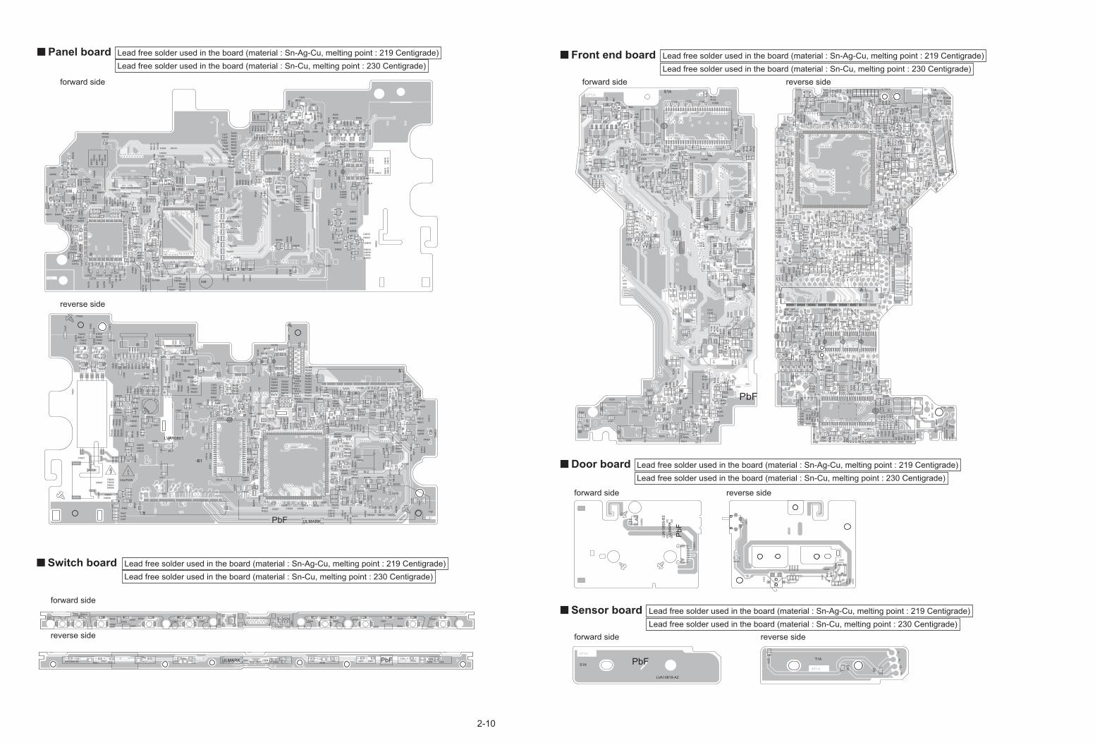
2-10
Door board Lead free solder used in the board (material : Sn-Ag-Cu, melting point : 219 Centigrade)
Lead free solder used in the board (material : Sn-Cu, melting point : 230 Centigrade)
Sensor board Lead free solder used in the board (material : Sn-Ag-Cu, melting point : 219 Centigrade)
Lead free solder used in the board (material : Sn-Cu, melting point : 230 Centigrade)
Panel board Lead free solder used in the board (material : Sn-Ag-Cu, melting point : 219 Centigrade)
Lead free solder used in the board (material : Sn-Cu, melting point : 230 Centigrade)
Front end board Lead free solder used in the board (material : Sn-Ag-Cu, melting point : 219 Centigrade)
Lead free solder used in the board (material : Sn-Cu, melting point : 230 Centigrade)
Switch board Lead free solder used in the board (material : Sn-Ag-Cu, melting point : 219 Centigrade)
Lead free solder used in the board (material : Sn-Cu, melting point : 230 Centigrade)
forward side
forward side
reverse side
forward side reverse side
forward sideforward side reverse side
reverse side
reverse side
LV
A10800-B
3
16
PbF
MA
RK
UL
CN
85
1
CN
85
2
S8501
R8510IC851
R8505
R8504
R8506
Q8501
R8508
R8509
R8502
R8503
S8502
R8501
R8507
C569
CN551
D563
TP561
D552
C553
D561
S559
D557D556
S558
S553
D553D562
S555 S556S557S552S554
S551
C551
D560D559 D558
D551
D554 D555
IC551
LVA10801-B2 C568
C558
C564C563 C565 C557C567C560
C561C559 C566 C562
C556 C555PbFMARKUL C554R553 R554R552
R556R557
R555
R551 C552R558
1P1AS1A
R2
25
R306
R22
R330
R9
2
R372
R123
R121
R2
22
R2
18
PbF
S1
R1
59
Q303
R116
R392
R301
R1
02
R9
9
R9
8
C107
R1
91
R1
92
R124
R142
R1
81 R
17
9
R1
48
D8
R422
R419
R4
16
R4
11
D7
R4
10
R4
04
R4
03
R4
02
C1
43
C235
R305
R397
R3
96
D6
C232
R3
91
C150
C229
C228
C225
R3
85
R384
R383
R3
80
R3
76
R3
75
C175
R3
71
C220
R3
68
R367
C219
C2
18
C216
R364 R362
R3
61
R3
60
R1
76
R3
58
R351
R350
R3
28
C210
R323
R3
20
R319
C2
07
R3
16
C198
Q2
R233
R311
R3
10
C197C195
C2
00
R3
59
C2
01
L3
02
K12
R229
K1
35
K1
36
R149
K111
K112
R34
R8
9
C142
R87
C155
R86
R3
02
C151
C136
C135
C139
C1
38
K1
42
K1
41
IC5
02
IC5
01
R231 Q11
R5
3 R5
2
X3
54
K121
D2
D1
R3
7R
36
K1
06
K1
07
C4
8
R51
R111
R112
R113
C52IC307
C26
C25
C179
K11
0
K1
09
C128
C127
Q3
02
C126
R1
80
R169
R204
R152
R2
03
C65
C63
C129C133
R2
11
R150
R151
R163
TH491
R1
65
R168
K1
08
K1
38
C111
R184
R2
65
C19
R1
70
C132
C60
R143
C9
4
C20
C1
37
C131
C1
30
K11
3
IC399
Q3
01
C1
34
R2
12
R2
14
IC398
C51
C110
R1
83
R1
77
R1
78
C79
C78
R1
33
C77
C76
R132
R131
R164
R1
29
R11
9
C1
20
R146
R1
44
R1
38
C178
R268 R267
C8
1
K1
03
C8
2
X3
51
C9
8
C9
7
C9
6
R145
C9
5
C1
77
IC4
81
R171
R64
R2
09
R2
08
R68
R6
0
R7
0
R7
1
R63
R269
R59
C2
2
R11
7
Q1
03
Q1
01
R56
R6
5
R5
7
R6
1
R62
Q1
04
R5
8
Q102
R7
7
R2
07
K1
02
4P1AT1A
EI
I
D
LVA10819-
H
H
F
F
E
D
c
G
G
B
A
B
c
A
A1
Ye
llow
White
R8
2
SW3_PAD
SW
2_
PA
DS
W1
_P
AD
SW
_G
ND
R1
20
R1
07
C1
22
C1
21
R2
19
R2
13
SW
1_
SW
2_
SW1__
R200
R215 R216
C2
30
RFGND
RFVCC
TP
10
1
C2
31
C11
4
C113
C11
2
R115
C109
R1
25
R110
K6
TO
UT
TIN
FO
UT
FIN
TU
BU
YA
KI2
R100
TP
85
R1
88
R1
87
C1
05
C173
C1
74
K4
K3
K2
CN
101
R1
58
K1
39
R9
7
R9
6
R9
5
C104
C224C103
IC3
01
TP98
R4
23
R421
R4
20
R4
18
R4
17
C2
41
TP97
K8
C240
TP94
K7
C239
TP92
IC5
R4
13
R4
12C2
38
C237
TP
91
C236
R408
IC4
R4
06
TP
89
R405
TP88
TP87
TP
84
R4
00
C233
R399
TP
82
R394R393
TP
10
7
TP81
TP80
C2
27
C149
TP79
R3
88
D1.2VTP78
R387
R386
Q7
R382
R381
TP
77
R3
79
R378
TP
76
C1
47
C2
23
C222
C146
C1
44
R3
69
Q6
R3
66
TP75
R365
C2
17
C234
CN
1
C215
C2
14
P3
.3V
C141C140
TP
73
R3
57
R3
55
C226
TP106
TP72
R352
TP71
Q4
TP69
TP68
R329
TP
67
TP66
C1
64
C211
TP64
C1
62
TP63
TP
62
R325
TP61
R3
24
K1
0
WO
OF
ER
R3
21
C170
C208
R318
C206
R3
17
C205
C1
99
IC1
R315
R314
R3
13
R312
R309
TP60
TP59
TP
58
R2
64
R1
03
C1
96
USBNEN
PR
TO
UT
DA
TA
2D
ATA
3C
MD
CL
KD
ATA
0D
ATA
1
CD
WP
MO
NI7
MO
NI6
MO
NI5
MO
NI4
MONI3MONI2MO
NI1
R307
MO
NI0
S3
.3V
AD
OU
T3
Q9
R2
9
R2
8
R2
7
DP
TP
10
8
Q8
TP105
K9
A5
V
F_
LC
H
S3
.3V
_
RE
AR
_R
CH
RE
AR
_L
CH
K1
28
K1
27
K1
26
K1
25
F-R
CH
DG
ND
_7
DG
ND
_6
UC
S
SA
CKSC
LK
C176
R49
R4
8
C2
4
R174
TS
UB
UY
AK
I_S
EL
DD
ATA R47
Q1
05
DD
ATA
0
R2
17
IC4
00
BC
K0
C145
C1
68
C1
67
R220
R8
8
TP
57
LRCLK0
TP30R8
5
TP
32
0
R9
0R
22
3
DR
VC
NT
CD
/DV
D
DC
LK
0
R226
C1
65
R1
04
C148
PCMCLK0
AOUT0
IC7
R1
56
X353
C161
L3
03
C158
D2V_1
D-
C1
56
C1
6
C15
R5
0
K105
K104
C1
59
C88
K1
31
Q107Q106
R7
9
EP
CS
IC3
08
USBCLK
CN
40
3
R2
5R
23
R1
35
R21
R182
R2
05
R201
C125
IC304
R1
27
R3
1
R3
3
R1
26
C119
R1
73
R189
R190
C14C13
C11C12 C9 C8
C7
R1
72
C6
C5
C4
EP
SK
CENTER
MG
ND
M8
V
M5V
D5V
R2
28
S5
V
R227
A9
V
DA
C5
DA
C4
DGND1
DA
C3
DA
C2
DA
C1
SW
4_
SW
3_
LR
MU
TE
CP
UR
ST S2
UD
TU
2S
DT
SC
S
TX
IC3
R166
R167
C3
C2
R147
CN
40
1
K1
37
K124
K1
34
K133
K1
32
K1
20
K11
9K
11
8
K117
K11
4
R194R1
93
VH
AL
F
K11
5
R1
30
TU
BU
YA
KI
TP8
TP19
TP
18
TP
17
TP16
TP
20
TP15TP14
TP
21
TP12
TP11TP10
TP
1
TP
2
TP
3
TP
4
TP5
TP
6
TP
7
TP
9
C3
2
C3
1
R93
R94
R55R54
R198
R197
R1
96
C1
8
CLKO
DL
D-
DLD+
NEXWE
C102
CN
2
R134
C8
0
C101
R1
37
TP325
C11
7
C11
8
C11
6
C1
00
TP22
C58
C66
C7
4
TP317
R1
62
R136
R141
R140
R139
C67
TP316
C99
R1
54
R155
C7
5
R1
57
C9
0
C8
9
C87
C8
5
C86
TP
13
C83
C84
R46
C7
0C
93
R118
C21
C1
7
R76
C6
9
C5
0
CLD-
C9
1
C47
R3
5
C9
2
CL
D+
C1
R206
C7
2
R153
R1
60
RF
+
RF
-
R73
EP
DIO
C7
1C
68
TP
31
9
AG
ND
_1
R2
10
TE
MP
DE
T
C7
3
C115
IC3
02
R6
9
R72
AC
C5
V
R128
CN402
R67
TP
31
8
C2
3
R161
R6
6
K1
01
R1
95
1P2B
S2B
D509
D508
D4611
R4631
R4756
R4756
C5061
C5060
C438
C437
C5057
C5056
B405
R5
11
4
R5
11
3
C5058
D5002
C5315
C5312
B408
C5059
D507 D506
C507
R5036
R5035
R5034
C417
C416
C5311
C5051
Q5002
R5011
R4005
R4008
CN504
C506
R5004
R5003
R5002
Q4605
R4629
Q4607
R4627
R4766
R4764
R4765
R5304
R5078
RA506
IC504
C4735
C436
RA508
RA507
RA
505
RA504
RA503
RA502
RA501
R5101R5102 R529R527
C505
C5053
R5028
R5204
R4708
R4712
C5064
IC451
TP494
R521
C504
C503
R520
R519
Q507
C502
R524
R525
R523
Q506
R522
IC513
R4731
R4728
R4729
R4730
TP
481
TP
480
R5076
R5075
R405
R5024
R5023
Q4601
Q4604
R4625
D4608
R4624Q4602
R4623
C4633
R4622
Q4603
C4634
R5206
R5207
R5208
R5209
R5210
R5211
R5201
R5202
C5306
C5309
R5088 C5043
IC473
R5073
IC503
R4308
C5042
C5041
C5040
X5002
IC502
Q401
R432
C407
R435
R437
R416
R419
R425
D402
R414
R418
R433
TP479
R426
R450
R422
C401
TP478
R411
R401
TP476
R427
R415
C410
R440
TP474
R403
TP473
R428
R413
R439
TP471
R402
R442
TP470
R429
R407
R438
TP
469
R410
R441
TP468
R431
R404
TP
467
R412
TP466
R434
X401
R408
R421
C406
R449
R420
R430
C408 R409
TP
464
C405
R417
R406
R4619
C4715
C4709
R4741
R4732
C4718
R4742
C4707
R4720
R4733
C4710
R4751
R4703
C4723
C4708
C5054
R4702
C4702
R4719
R4723
R4713
C4706
R4701
C4705
R4714
C4713
C4711
C4703
C4725
R4715
R4722
IC471
R4759
C4722
R4738
R4743
R4721
C4717
R4716
R4718
C4716
C4721
R4739
R4717
C4714
R4755
C4724
R4752
R4740
R526 R528
R533R536
R535
R532
R531
R537
R530
R517
Q508
C501
R534
Q511
Q509
Q510
R518
R5067
R5066
C5027
C5029
R5064
R5005
R5006
R5022
R5086
R5071
R5070
R5069
R5072
R5014
R5015
R5029
R5027
R5018
R5017
R5032
R5026
Q4003
R4027
R4024
Q4007
D4001
C4003
C4004
R4031
C4017
R4032
TP402
C4015
R4003
R4028
R4009
R4011
C4016
R4026
R4018
Q4005 R4030
R4001
TP401
R4002
C4002
R4023
R4017
C4001
D4302
R4016
IC402
R4004
R4025
R4012
C4614
C4609C4608
C4611
R4615
IC461
IC462
C4603
C4616
C4610
C4615R4614
R4626
D4601
C4617
R4611
R4603
R4601
C4612
C4613
R4610
L4601
C4605
C4602
C4604
IC512
R5010
C5028
C5026
TP
501
C5310
R5302
D5001L
5001
4P2B
T2B
-B1
B
B
W-2
W-1
A
LVA10801
CAUTION
A
B411
C5063
C5062
C516
C434
C435C
4733
C4734
C5055
C5313
B409
C5314
C514
C513
C508
C4732
C4731
C5049R455
C415
C414
C5052
R5033
C433
C432
D4609
D4610
R4630
PbF MARKUL
C431
C430
C429
C428
C427
C426
R457
R456
C422
C421
C423
TP502
R436
R5001
R4767
CN503
RA522
RA521
RA520
C5050
IC411
CN501
R5105
R4726R4725R4724
D4002
C515
RA
509
CN
403
C5044
CN404
R511
0
R511
2
R424
R4710
R4709
R4706
R4705
R4704
TP523
R5009
TP522
R5079
L5005
C5039
C5012C5011
C5010C5009
C5008
C5007
C5006
C5004
C5005
C5003
C5002
C5001
IC501
R5030
R5106
L5004
C5305
C5304
C5303
C5302
C5301
C5308
C5307
C402
L4001
R5085
R4748
R4749
R4307
R4303
R4305
R4301
C4102
IC412
L401
R451
C409
C412
IC452
R423 Q403
Q402
D401
R454C411
R445
R453
R443
R444
R448
R452
C404
R446
C413
C403 R447
TP
521
R4621D4607
D4606
R4620
IC472
R4754
C4727
C4726
D4303
C4701
C4728
C4704
C4729
C4712
R4763
R4707
C4635
B403
L4702
C4720
B402
C4730
C4719
R5104
K502
D504
D505
CN502
D503
C510
C512
D502K501
C511
K503 C
509
K504
R5058
C5017
C5019
C5018
C5020
C5021
R5107
C5048
C5047
C5046
C5045
R5103
Q5001
R5084
R5083
C5038
C5037
R5082
C5036
C5035
C5032
C5031
C5030
C5025
C5024
C5023
C5022
R5057
R5061R5060
R5059
R5063
R5062
R5065
R5068
C5034
C5033
X5001
R5008
R5007
R5100
R5099
R5098
R5097
R5092
R5087
R5081
R5074
R5077
R5080
R5016
R5013
R5019 R5021
R5020
R5031
R5038
R5025
R5037
R5048
R5044
R5043
C4307
TP408
TP413
D4301
TP
436
R4209
R4035
R4212
R4362
R4368
R4361
R4022
TP414
Q4004
TP417
R4015
C4302
R4013
R4360
C4101
R4019
C4009
R4107
R4367
R4021
R4359
C4310
R4366
R4211
TP
434
R4208
R4358
R4210
L4002
C4308
C4014
C4303
R4034
C4305
R4201
CN401
R4204
R4108
TP412
R4110
R4365
R4029
TP437
C4306
R4020
Q4001
R4109
TP407
TP431
R4033
L4302
C4006
C4013
TP
435
R4202
C4311
TP409
R4010
C4008
R4014
Q4006
TP411TP410
R4207
L4301
R4206
B401
C4309
R4203
C4304
R4364
Q4002
C4012
C4010
R4205
R4363
TP416
TP404
C4301
TP415
C4619
C4607
C4618
R4609
C4625
C4624
IC464
R4606
R4608
C4627
C4623
IC463
R4605
TP518
D4605
C4622
R4604
R4613
C4626R4617
C4606
C4629
L4602
D4604
D4603
C4601
R4616
R4618
TP
520
R4612
C4621C4620
C4631
C4628
R4607
TP
519
C4630
T4601
D4602
C4632
R5012
C5015
C5016
C5013
C5014
R5050R5049
IC511
1P1A
S1A
LVA10819-A2
PbF4P1A
T1A
D9
D10
D11
1
3
G
2

< M E M O >

(No.MA427SCH<Rev.001>)Printed in Japan
VPT
Mobile Entertainment Division 10-1,1chome,Ohwatari-machi,Maebashi-city,Gumma-ken,371-8543,Japan
Victor Company of Japan, Limited
Related Documents