ISEL INSTITUTO SUPERIOR DE ENGENHARIA DE LISBOA SERVIÇO DE DOCUMENTAÇÃO E PUBLICAÇÕES INSTITUTO SUPERIOR DE ENGENHARIA DE LISBOA Área Departamental de Engenharia de Electrónica e Telecomunicações e de Computadores JPEG Decoder implementation on FPGA using Dynamic Partial Reconfiguration Tiago Augusto Nunes Rodrigues (Licenciado) Trabalho Final de Mestrado para Obtenção do Grau de Mestre em Engenharia de Electrónica e Telecomunicações Orientador: Professor Doutor Mário Pereira Véstias Júri: Presidente: Professora Doutora Maria Manuela Almeida Carvalho Vieira Vogais: Professor Doutor José Manuel Peixoto do Nascimento Junho de 2015

Welcome message from author
This document is posted to help you gain knowledge. Please leave a comment to let me know what you think about it! Share it to your friends and learn new things together.
Transcript
ISEL
INSTITUTO SUPERIOR DE ENGENHARIA DE LISBOA SERVIÇO DE DOCUMENTAÇÃO E PUBLICAÇÕES
INSTITUTO SUPERIOR DE ENGENHARIA DE LISBOA Área Departamental de Engenharia de Electrónica e
Telecomunicações e de Computadores
JPEG Decoder implementation on FPGA using
Dynamic Partial Reconfiguration
Tiago Augusto Nunes Rodrigues
(Licenciado)
Trabalho Final de Mestrado para Obtenção do Grau de Mestre em Engenharia de Electrónica e
Telecomunicações
Orientador:
Professor Doutor Mário Pereira Véstias
Júri:
Presidente: Professora Doutora Maria Manuela Almeida Carvalho Vieira
Vogais: Professor Doutor José Manuel Peixoto do Nascimento
Junho de 2015

i
Abstract
This thesis describes a study conducted in Reconfigurable Computing using a Field-Programmable
Gate Array (FPGA). Reconfigurable Computing is a concept almost as old as high-speed electronic
computing itself. To explore the practical aspects of the concept, a Baseline JPEG image decoder was
implemented over a Zynq™-7000 family FPGA. After using traditional methods for the design,
implementation and debugging of static decoder logic, the work path was set to adapt the decoder to be
implemented on the same FPGA using methods based on Dynamic Partial Reconfiguration. Using this
approach the main objective was to develop a working decoder with only a subset of the used resources of
the FPGA when compared to static implementation of the similar decoder. The dynamic partial
reconfiguration brings some additional complexity to the system resulting on two different decoders from
a macro perspective view but globally relying on the same design considerations and that share the
majority of the internal modules. The steps to achieve the objective are described in order to clarify the
dynamic partial reconfiguration process and to eventually open new design possibilities that can be
exploited in different application scenarios. The thesis also explores the development of auxiliary systems
to enable the ability to decode direct .jpg files and present them on a VGA monitor.
Keywords
Field-Programmable Gate Array, Dynamic Reconfiguration, Reconfigurable computing, JPEG image
decoding.
ii
Resumo
Esta tese descreve o estudo realizado sobre o tema de Sistemas Computacionais Reconfiguráveis
utilizando Field-Programmable Gate Array (FPGA). Sistemas Computacionais Reconfiguráveis é um
conceito tão antigo como a computação utilizando circuitos electrónicos. Para explorar os aspetos práticos
do conceito, foi implementado um descodificador de imagens codificadas em sistema Baseline JPEG
sobre uma FPGA da família Zynq™-7000. Realizado todo o trabalho de desenho, implementação e
depuração do descodificador utilizando métodos tradicionais de implementação estática da lógica na
FPGA, foi posteriormente realizado o trabalho de adaptação do descodificador desenvolvido para
implementação na mesma FPGA utilizando métodos de implementação com reconfiguração parcial
dinâmica. Este novo método tem como objetivo principal a realização de um descodificador funcional
utilizando apenas uma parte dos recursos lógicos da FPGA quando comparado com a implementação
estática do descodificador. A utilização de reconfiguração dinâmica tem como consequência um
incremento da complexidade do sistema, originando, numa perspetiva macro, diferenças entre ambos os
descodificadores, mas globalmente baseados nos mesmos critérios de desenho e partilhando grande parte
dos módulos internos. São ainda descritos os passos para atingir o objetivo, de forma a clarificar o
processo de reconfiguração parcial dinâmica para uma aplicação em eventuais novos critérios de projeto e
diferentes cenários de aplicação. Esta tese explora ainda o desenvolvimento de sistemas auxiliares que
permitem a descodificação direta de ficheiros .jpg e a sua apresentação num monitor VGA.
Palavras-chave
Field-Programmable Gate Array, Reconfiguração Dinâmica, Sistemas Computacionais
Reconfiguráveis, decodificação de imagens JPEG.

iii
Acknowledgement
During the many hours I have spent on this journey from which this work is the epilog I had the
amazing support of my loved one, incredible wife and the mother of my two beautiful children, for all
that I am deeply thankful.
I would like to thank my mother for making this event possible on my life, for all the love and
support on my previous studies sometimes in difficult moments.
I would like to thank my close family, my sister, my father-in-law, mother-in-law and my sister-in-
law for all the mental and logistic support that permitted me to complete this work.
I would also like to thank my mentor Prof. Dr. Mário Véstias for the ideas on this work and the
support on the moment when things seem to come to a stall, giving the correct push to complete this
work.
iv
Table of contents
ABSTRACT ................................................................................................................................................ I
RESUMO ................................................................................................................................................... II
ACKNOWLEDGEMENT ...................................................................................................................... III
TABLE OF CONTENTS ........................................................................................................................ IV
TABLE OF FIGURES ........................................................................................................................... VII
LIST OF TABLES ..................................................................................................................................... X
LIST OF ACRONYMS ........................................................................................................................... XI
1 INTRODUCTION ........................................................................................................................ 1
2 DYNAMIC PARTIAL RECONFIGURATION ........................................................................ 5
2.1 RECONFIGURABLE COMPUTING SYSTEMS ....................................................................... 5
2.1.1 The dynamic reconfigurable FPGA technology .................................................. 6
2.2 DYNAMIC PARTIAL RECONFIGURATION OF FPGA .......................................................... 9
2.2.1 Difference-Based Partial Reconfiguration .......................................................... 9
2.2.2 Dynamic Partial Reconfiguration application examples ..................................... 9
2.2.3 Xilinx Dynamic Reconfiguration Support Tools .............................................. 11
2.2.4 Reconfiguration Time ....................................................................................... 15
2.2.5 PL Reconfiguration on Zynq®-7000 AP SoC .................................................. 16
2.2.6 Exercises on Dynamic Reconfiguration ............................................................ 17
2.2.6.1 Development of a LED scrolling shifter .................................................. 17
3 JPEG DECODER DEVELOPMENT ....................................................................................... 23
3.1 JPEG IMAGE COMPRESSION OVERVIEW ........................................................................ 23
3.1.1 JPEG Encoder structure .................................................................................... 24
3.1.2 RGB to Y′CBCR transformation (1) ................................................................... 24
3.1.3 Downsampling (2) ............................................................................................. 25
3.1.4 Discrete Cosine Transform (3) .......................................................................... 27
3.1.5 Quantization(4) ................................................................................................. 29
3.1.6 Zig-Zag ordering (5) ......................................................................................... 30
3.1.7 Entropy encoding .............................................................................................. 30
3.2 JPEG DECODER ARCHITECTURE .................................................................................... 34
3.2.1 JFIF File format ................................................................................................ 34
3.2.2 Encoded Stream ................................................................................................ 39
3.2.3 Stuffing .............................................................................................................. 39
3.3 DEVELOPED STATIC JPEG DECODER ............................................................................. 40
3.3.1 JPEG Decoder top entity ................................................................................... 40
v
3.3.2 Module sr_input ................................................................................................ 42
3.3.3 Module huffman_decoder ................................................................................. 43
3.3.3.1 JFIF Data Reader ...................................................................................... 43
3.3.3.2 Stuffing detection ..................................................................................... 48
3.3.3.3 Entropy decoding ..................................................................................... 48
3.3.3.4 Huffman decoder ...................................................................................... 49
3.3.3.5 Dequantization .......................................................................................... 55
3.3.4 Module zrl_decoder .......................................................................................... 55
3.3.5 Module idct_core .............................................................................................. 58
3.3.6 Module mcu_upsampling .................................................................................. 61
3.3.7 Module YCbCr2RGB........................................................................................ 63
4 DEVELOPED DPR JPEG DECODER .................................................................................... 65
4.1 RECONFIGURABLE MODULES INFORMATION PROCESSING ............................................ 65
4.2 RECONFIGURABLE DECODING PROCESS ........................................................................ 66
4.3 RECONFIGURABLE MODULES DEFINITION ..................................................................... 67
4.4 JPEG DECODER TOP ENTITY .......................................................................................... 69
4.4.1 JPEG Decoder reconfiguration interface........................................................... 69
4.4.2 Reconfigurable Partition Interface .................................................................... 70
4.4.3 Decoding Control States ................................................................................... 71
4.4.4 Reconfigurable Modules Processing Phases ..................................................... 72
4.4.5 Memory Organization ....................................................................................... 72
4.4.6 RP Header_reader module ................................................................................ 77
4.4.7 RP Huffman_decoder module ........................................................................... 77
4.4.8 RP Dezigzag_Dequantitize module .................................................................. 79
4.4.9 RP IDCT_2D module ........................................................................................ 81
4.4.10 RP YCbCr2RGB_Upsampling module ........................................................ 82
4.4.11 Simulation and Debugging of the Reconfigurable System ........................... 84
5 IMPLEMENTATION AND RESULTS ................................................................................... 86
5.1 PROCESSOR SYSTEM INTERFACE DETAILS ..................................................................... 86
5.1.1 Static Implementation PS Interface ................................................................... 86
5.1.2 Reconfigurable Implementation of the PS Interface ......................................... 88
5.2 AUXILIARY MODULES IMPLEMENTATION ...................................................................... 90
5.2.1 Reconfigurable implementation auxiliary modules .......................................... 92
5.3 STATIC IMPLEMENTATION RESULTS .............................................................................. 92
5.4 RECONFIGURABLE JPEG DECODER IMPLEMENTATION ................................................. 93
5.4.1 Implementation results ...................................................................................... 93
Decoding performance .............................................................................................. 95
5.4.2 ................................................................................................................................ 95

vi
6 CONCLUSIONS AND FUTURE WORK .............................................................................. 101
APPENDIX ............................................................................................................................................. 103
A. HUFFMAN TREE EXAMPLE ........................................................................................... 104
B. HUFFMAN DECODER MEMORY ORGANIZATION EXAMPLE ......................................... 105
C. RECONFIGURABLE MCU DECODING EXECUTION TIME EXAMPLE .............................. 106
BIBLIOGRAPHY .................................................................................................................................. 107
vii
Table of figures
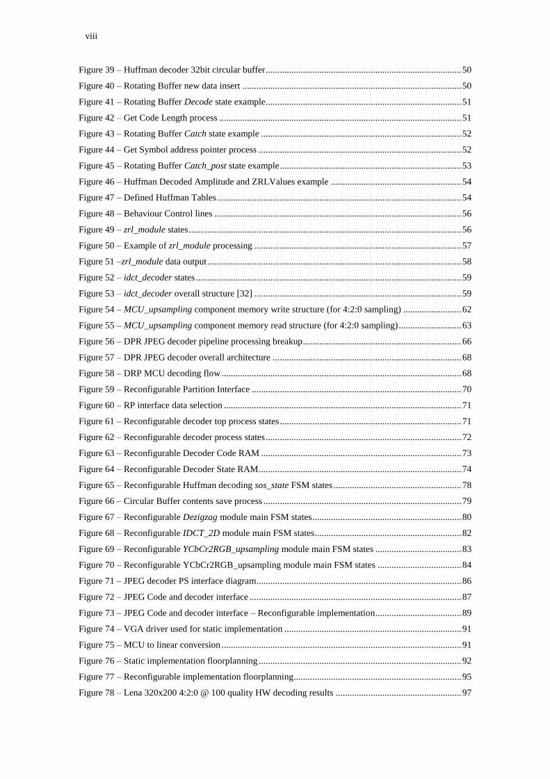
Figure 1 – ZedBoard block diagram [4] ....................................................................................................... 2
Figure 2 – Illustration taken from “The Fixed Plus Variable Structure Computer paper” ........................... 6
Figure 3 – Generic FPGA architecture [6] ................................................................................................... 6
Figure 4 – Typical Logic [7] ........................................................................................................................ 7
Figure 5 – Xilinx DPR design flow ............................................................................................................ 11
Figure 6 – PlanAhead cover area on a Partial Reconfiguration Project flow ............................................. 12
Figure 7 – Z-7020 device organization ....................................................................................................... 13
Figure 8 – LED scrolling shifter using DPR .............................................................................................. 18
Figure 9 – PlanAhead selection of Reconfigurable Project ........................................................................ 19
Figure 10 – Reconfigurable Partition Area Definition ............................................................................... 20
Figure 11 – FPGA Configuration using PCAP ........................................................................................... 21
Figure 12 – Boot sequence and the System Configuration ......................................................................... 22
Figure 13 – JPEG Encoder ......................................................................................................................... 24
Figure 14 – Lena image decomposed to Y’CBCR color space .................................................................... 25
Figure 15 – Y′CBCR downsampling formats............................................................................................... 26
Figure 16 – JPEG Image subsampling MCU ............................................................................................. 26
Figure 17 – JPEG Image subsampling MCU ............................................................................................. 27
Figure 18 – Fast DCT transformation ......................................................................................................... 28
Figure 19 – 2D DCT function representation of the weighted pixel values [30] ........................................ 29
Figure 20 – Quantization of a 2D DCT block ............................................................................................ 29
Figure 21 – Zig-Zag vector stream of a 2D DCT block [27] ...................................................................... 30
Figure 22 – DPCM of DC coefficient ........................................................................................................ 31
Figure 23 – JPEG Baseline sequential decoder .......................................................................................... 34
Figure 24 – Simplified JFIF file format ...................................................................................................... 35
Figure 25 – JFIF marker segments ............................................................................................................. 35
Figure 26 – Stuffing detector ...................................................................................................................... 39
Figure 27 – JPEG Baseline module description files ................................................................................. 40
Figure 28 – jpeg_decoder top entity ........................................................................................................... 40
Figure 29 – Module communication lines .................................................................................................. 42
Figure 30 – sr_input module data ............................................................................................................... 43
Figure 31 – sr_input module structure ....................................................................................................... 43
Figure 32 – Header reading marker states .................................................................................................. 44
Figure 33 – Quantification table reading process ....................................................................................... 44
Figure 34 – Huffman table reading process ................................................................................................ 45
Figure 35 – Frame information reading process ......................................................................................... 47
Figure 36 – Frame components information reading process ..................................................................... 47
Figure 37 – Scan reading process ............................................................................................................... 48
Figure 38 – Huffman decoding sos_state FSM states ................................................................................ 49
viii
Figure 39 – Huffman decoder 32bit circular buffer .................................................................................... 50
Figure 40 – Rotating Buffer new data insert .............................................................................................. 50
Figure 41 – Rotating Buffer Decode state example .................................................................................... 51
Figure 42 – Get Code Length process ........................................................................................................ 51
Figure 43 – Rotating Buffer Catch state example ...................................................................................... 52
Figure 44 – Get Symbol address pointer process ....................................................................................... 52
Figure 45 – Rotating Buffer Catch_post state example .............................................................................. 53
Figure 46 – Huffman Decoded Amplitude and ZRLValues example ........................................................ 54
Figure 47 – Defined Huffman Tables ......................................................................................................... 54
Figure 48 – Behaviour Control lines .......................................................................................................... 56
Figure 49 – zrl_module states ..................................................................................................................... 56
Figure 50 – Example of zrl_module processing ......................................................................................... 57
Figure 51 –zrl_module data output ............................................................................................................. 58
Figure 52 – idct_decoder states .................................................................................................................. 59
Figure 53 – idct_decoder overall structure [32] ......................................................................................... 59
Figure 54 – MCU_upsampling component memory write structure (for 4:2:0 sampling) ......................... 62
Figure 55 – MCU_upsampling component memory read structure (for 4:2:0 sampling) ........................... 63
Figure 56 – DPR JPEG decoder pipeline processing breakup .................................................................... 66
Figure 57 – DPR JPEG decoder overall architecture ................................................................................. 68
Figure 58 – DRP MCU decoding flow ....................................................................................................... 68
Figure 59 – Reconfigurable Partition Interface .......................................................................................... 70
Figure 60 – RP interface data selection ...................................................................................................... 71
Figure 61 – Reconfigurable decoder top process states .............................................................................. 71
Figure 62 – Reconfigurable decoder process states .................................................................................... 72
Figure 63 – Reconfigurable Decoder Code RAM ...................................................................................... 73
Figure 64 – Reconfigurable Decoder State RAM ....................................................................................... 74
Figure 65 – Reconfigurable Huffman decoding sos_state FSM states ....................................................... 78
Figure 66 – Circular Buffer contents save process ..................................................................................... 79
Figure 67 – Reconfigurable Dezigzag module main FSM states ................................................................ 80
Figure 68 – Reconfigurable IDCT_2D module main FSM states ............................................................... 82
Figure 69 – Reconfigurable YCbCr2RGB_upsampling module main FSM states ..................................... 83
Figure 70 – Reconfigurable YCbCr2RGB_upsampling module main FSM states .................................... 84
Figure 71 – JPEG decoder PS interface diagram ........................................................................................ 86
Figure 72 – JPEG Code and decoder interface ........................................................................................... 87
Figure 73 – JPEG Code and decoder interface – Reconfigurable implementation ..................................... 89
Figure 74 – VGA driver used for static implementation ............................................................................ 91
Figure 75 – MCU to linear conversion ....................................................................................................... 91
Figure 76 – Static implementation floorplanning ....................................................................................... 92
Figure 77 – Reconfigurable implementation floorplanning........................................................................ 95
Figure 78 – Lena 320x200 4:2:0 @ 100 quality HW decoding results ...................................................... 97
ix
Figure 79 – Lena 320x200 4:2:0 @ 50 quality HW decoding results ........................................................ 98
Figure 80 – Lena 320x200 Grayscale @ 100 quality HW decoding results ............................................... 98
Figure 81 – Test image 1 decoding time variation with per configuration decoded MCU ....................... 100

x
List of tables
Table 1 – JPEG-Specification defined compression processes .................................................................. 23
Table 2 – MCU component organization and size ..................................................................................... 27
Table 3 – Baseline JPEG coefficient magnitude classification table .......................................................... 31
Table 4 – Example of symbols encoding .................................................................................................... 32
Table 5 – Example of Huffman code tables ............................................................................................... 32
Table 6 – Example of Huffman coding of symbols .................................................................................... 32
Table 7 – JPEF markers identified by the decoder ..................................................................................... 36
Table 8 – Frame Sampling Factor identification ........................................................................................ 38
Table 9 – Static jpeg_decoder module interface signals ............................................................................ 41
Table 10 – Output Sampling Factor identification ..................................................................................... 42
Table 11 – JPEG decoder tasks minimum processing structure ................................................................. 65
Table 12 – JPEG decoder isolated module resources estimation ............................................................... 67
Table 13 – jpeg_decoder module interface signals .................................................................................... 69
Table 14 – Reconfigurable Module ID ....................................................................................................... 70
Table 15 – JPEG Core interface registers ................................................................................................... 87
Table 16 – JPEG Core interface registers ................................................................................................... 88
Table 17 – JPEG Core Status register details – Reconfigurable implementation ....................................... 88
Table 18 – JPEG Core Data register details – Reconfigurable implementation......................................... 88
Table 19 – Static JPEG decoder implementation resources ....................................................................... 93
Table 20 – Reconfigurable JPEG decoder implementation resources ........................................................ 93
Table 21 – Reconfigurable vs Static ........................................................................................................... 93
Table 22 – Used resources by the Reconfigurable partition modules ......................................................... 94
Table 23 – Reconfigurable vs Static Resources usage ............................................................................... 94
Table 24 – Reconfigurable JPEG decoder implementation maximum frequency ...................................... 95
Table 25 – Decoding performance reference images ................................................................................. 95
Table 26 – System Reconfiguration time ................................................................................................... 99
Table 27 – Decoding times for Lena image 320x200 4:2:0 @ 100 quality factor ...................................... 99
Table 28 – Decoding times for Lena image 320x200 4:2:0 @ 50 quality factor ........................................ 99
Table 29 – Decoding times for Lena image 320x200 Grayscale @ 100 quality factor .............................. 99
xi
List of acronyms
ALM Adaptive Logic Module
ALU Arithmetic Logic Unit
ARM Advanced RISC Machine
ASIC Application Specific Integrated Circuit
BRAM Block-RAM
CF Configuration Frame
CLB Configurable Logic Block
CPU Central Processing Unit
DCT Discrete Cosine Transform
DMA Direct Memory Access
DPCM Differential Pulse Code Modulation
DPR Dynamic Partial Reconfiguration
DHT Define Huffman Table marker
DQT Define Quantization Table marker
AC AC DCT coefficient
DC DC DCT coefficient
DSP Digital Signal Processing
EOB End-Of-Block
EOI End-Of-Image marker
F+V Fixed plus Variable Architecture
FPGA Field-Programmable Gate Array
FSBL First Stage Boot Loader
I/O Input/Output
ICAP Internal Configuration Access Port
IDCT Inverse Discrete Cosine Transform
IOB Input/Output Block
ISE Integrated Synthesis EnviromentEnvironment
JFIF JPEG File Interchange Format
JPEG Joint Photographic Experts Group
LUT Look-Up Table
MCU Minimum Coded Unit
MIO Multiplexed Input/Output
PCAP Processor Configuration Access Port
PL Programmable Logic
PLD Programmable Logic Device
PS Processingor System
RAM Random Access Memory
RLE Run-Length Encoding

xii
SDR Software Defined Radio
SoC System-on-Chip
SRAM Static Random Access Memory
VHDL VHSIC Hardware Description Language
VHSIC Very High Speed Integrated Circuit
VLC Variable Length Code
ZRL Zero Run-length
Introduction 1
1 Introduction
Since its invention in the 80’s, the Field-Programmable Gate Array (FPGA) keeps finding its way to
all sorts of applications. The great flexibility, cost efficiency and excellent performance when compared
with microprocessor based approaches, makes the FPGA extremely convenient on the system
development level. When compared with Application Specific Integrated Circuit (ASIC), FPGAs are
historically slower and less energy efficient [1] but due to the possibility of reconfiguration of the logic
fabric at development level, the use of FPGA is still the best way to deploy limited production, design
flexible systems with minimal time-to-market and the possibility to reprogram the logic ‘on the field’.
Like ASICs, the parallelism capabilities make these components very useful in extreme processing tasks
like signal and image processing.
Due to its intrinsic nature, software based approaches compared with the hardware approaches, like
on FPGAs, are still seen as the only solution on systems that require flexibility. Since the introduction of
programmable general purpose computers, these software based systems can change their behaviours in a
flip of an eye, only by changing the running program, concept referred as reconfigurable computing. A
new concept of High-Performance Embedded Reconfigurable Computing has emerged, that combines
FPGA and a Central Processing Unit (CPU) on heterogeneous systems referred to as System-on-Chip
(SoC). The FPGA technology is still somehow limited in the number of tasks it can perform due to the
number of hardware resources that can be implemented over the silicon chip, but these new
heterogeneous systems can dynamically reuse the programmable logic area and implement several
functions, increasing the flexibility of the hardware approach over pure software implementations. The
system used on the development of this thesis utilizes the new family of SoC platforms – Zynq® - from
Xilinx.
Zynq®-7000 AP SoC System Platform
Since 2011 Xilinx made available to the market a new reconfigurable SoC platform Zynq®-7000 AP
SoC. The platform consists of the powerful dual-core ARM Cortex-A9 processor based processing
system and the 28 nm Xilinx Programmable Logic. The ARM processor comes together with caches, on-
chip memory, external memory interfaces, Direct Memory Access (DMA) controller, a I/O configurable
MIO Multiplexer and input-output to the PL.
The Programmable Logic (PL) uses similar architecture to Artix-7 or Kintex-7 (depending on the
Zynq device) FPGA families consisting of configurable logic blocks, block random-access memories,
digital signal processing blocks (DSP), programmable input-output blocks, serial transceivers and analog-
to-digital converters (ADCs). The maximum operational frequency of the ARM is 667 MHz – 1 GHz, the
PL contains between 17 600 – 218 600 LUTs, 35 200 – 437 200 flip- flops, 240 – 2 180 kB block
random-access memories (given by the selected Zynq-7000 AP SoC device) [2]. The embedded processor
and the PL are on independent power supplies, with 1.0 V supply for the logic, 1.8 – 3.3 V for the input-
output buffer and 1.2 – 1.8 V for the external DDR memory interface [3].
2 Introduction
Previous FPGA families by Xilinx are in fact PLs with the possibility for on-chip processor add-in
(PL-centric architecture). The new Zynq®-7000 AP SoC is an FPGA platform built around the processor
(PS-centric architecture).
The PS can configure the PL on boot, reading the bitfile from several possible interfaces, Flash RAM,
SD card or JTAG interface. The dual-core processor can work in several operating configurations:
1) One core is operational and the second one is turned off using clock gating;
2) Both cores are operating. This multiprocessing cooperation can be symmetric, when both cores
are running the same Operating System (OS) and participate in the same operations (e.g.
multithread and multiprocess execution on a higher-level OS like Linux), or asymmetric, when
the cores are independent with different OSs (e.g. full featured OS and non-OS standalone bare-
metal application).
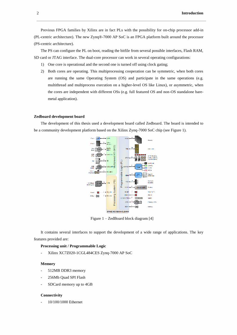
Zedboard development board
The development of this thesis used a development board called Zedboard. The board is intended to
be a community development platform based on the Xilinx Zynq-7000 SoC chip (see Figure 1).
Figure 1 – ZedBoard block diagram [4]
It contains several interfaces to support the development of a wide range of applications. The key
features provided are:
Processing unit / Programmable Logic
- Xilinx XC7Z020-1CGL484CES Zynq-7000 AP SoC
Memory
- 512MB DDR3 memory
- 256Mb Quad SPI Flash
- SDCard memory up to 4GB
Connectivity
- 10/100/1000 Ethernet
Introduction 3
- USB 2.0 USB-UART bridge
- Five Pmod expantion headers
- FMC connector
- Seven push buttons (2 PS, 5 PL)
- Eight switches (PL)
Display / Audio
- HDMI output
- VGA output with 12-bit colour interface
- 128x32 OLED Display
- Audio line-in, Line-out, headphone and Microphone
Motivation and Developed work
This thesis studies the static and the more recent technic based on Dynamic Partial Reconfigurable
(DPR) implementation methods for a baseline JPEG decoder on a FPGA device.
The idea behind this subject was to study in more detail the new implementation technics that over
the past decade become available on commercial FPGA technology. The image processing area has been
over the years one of the main application areas of the FPGA technology and with this work the objective
was to look at different approaches to current problems of these applications.
The first approach has the development and implementation of a working JPEG decoder on a develop
board using standard static implementation methods. Using the developed decoder as starting point, a new
decoder was developed suitable to be implemented using Dynamic Partial Reconfiguration.
The decoder developing approach used was, define all decoder functions, use existing code for some
of them (e.g. Huffman and IDCT decoding), develop the remaining and integrate all functions into the
system.
From the static implementation decoder, a dynamic reconfigurable implementation of a JPEG image
decoder was developed, adapting the existing functions. This implementation method main objective is to
explore the hardware reuse on FPGA.
The thesis is structured on the following way, after a brief introduction to dynamic reconfigurable
systems, the static decoder development is explained in detailed and from it the correct steps to obtain a
dynamic reconfigurable decoder. The results from both types of implementations where compared to
conclude on the advantages and possible disadvantages of the approach.

4 Introduction
Organization of the thesis
This thesis is organized in the following order;
Chapter 2 describes the concept of Dynamic Partial Reconfiguration, describes the SoC system used
for the work and the preparation work developed on reconfigurable systems.
Chapter 3 describes the JPEG decoder implemented in the development platform.
Chapter 4 describes the adaptation study and development of a JPEG decoder that fulfils the
requirements to be implemented on the reconfigurable system.
Chapter 5 presents the results that are then discussed and analysed in detail.
Chapter 6 presents the conclusions and suggestions for future work.
Dynamic Partial Reconfiguration 5
2 Dynamic Partial Reconfiguration
The need to increase the capability to implement more functions on the FPGA logic fabric is pushing
the technology to increase the transistor density of these devices. The development of SoC systems that
can reconfigure the logic fabric at runtime boosted the area of application for these systems due the
extreme flexibility and possible performance that can be achieved. Reconfigurable technologies have
indeed several advantages. These systems can reuse the same hardware and join the best of the software
and hardware approach of a problem, making the concept of reconfigurable computing a reality for the
hardware as it exists for software. A system now can be adapted during runtime if necessary. Normally
the logic fabric can be changed to implement different logic combinations to deal with problems like
decoding an image or adapt an interface to the type of information to be processed. However, the
reconfiguration of the logic fabric implies that system has to stop all tasks while it is reconfigured loosing
also all connections with the past states resulting on a cold start of the system after reconfiguration
finishes. These restrictions limit the use of reconfiguration on complex systems that use a large number of
logic components on the logic fabric to perform several tasks that are not related to each other. In these
cases, stopping all fabric tasks will have a great impact on the overall performance of the system. For
instance a router system that implements on hardware logic for the interface and routing tasks can be
made more flexible and power efficient by reconfiguring the logic on runtime to adapt the system to
specific usage of the number of ports used, type of protocols, routing algorithms. However, the
availability could be seriously affected if all system has to halt while a reconfiguration of the logic is
needed. This problem was in some way overcome by FPGAs that support Dynamic Partial
Reconfiguration. These FPGAs have the ability to change part of the logic configuration area while the
rest of the circuit remains active and running. This technology is a research subject since the 90s [1] and
is now commonly used in FPGAs, provided by Xilinx and Altera. The main advantages of the partial,
run-time reconfiguration are to add hardware flexibility and to reuse hardware area, allowing power and
production costs reductions. Also, the possibility to change the logic fabric at runtime without affecting
all the PL area gives the possibility to fulfil several different tasks on a dynamic scenario. This opens new
possibilities on the development of reconfigurable computing systems that in other way could not be
implemented.
2.1 Reconfigurable Computing Systems
Reconfigurability on a computational process means that the system is able to change hardware, or
parts of the hardware, either on a problem by problem basis or even during the lifetime of an algorithm
solving one problem instance. In software systems, reconfigurability has been accomplished with the
invention of the microprocessor based systems. As for most cases where a new area of technology
appears, there isn’t an exact system that can be accounted as the turning point. It’s fair to say that the idea
behind self-reconfiguring hardware have been developed consistently throughout the history of
computing since about 1960, beginning with what is frequently referenced under “distributed computing”
as the Fixed-Plus-Variable or just F+V computer develop in the University of California by Gerald Estrin
6 Dynamic Partial Reconfiguration
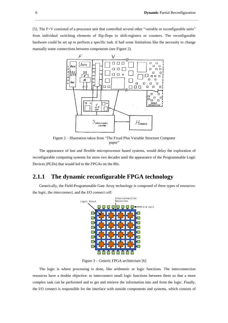
[5]. The F+V consisted of a processor unit that controlled several other “variable or reconfigurable units”
from individual switching elements of flip-flops to shift-registers or counters. The reconfigurable
hardware could be set up to perform a specific task. It had some limitations like the necessity to change
manually some connections between components (see Figure 2).
Figure 2 – Illustration taken from “The Fixed Plus Variable Structure Computer
paper”
The appearance of fast and flexible microprocessor based systems, would delay the exploration of
reconfigurable computing systems for more two decades until the appearance of the Programmable Logic
Devices (PLDs) that would led to the FPGAs on the 80s.
2.1.1 The dynamic reconfigurable FPGA technology
Generically, the Field-Programmable Gate Array technology is composed of three types of resources:
the logic, the interconnect, and the I/O connect cell.
Figure 3 – Generic FPGA architecture [6]
The logic is where processing is done, like arithmetic or logic functions. The interconnection
resources have a double objective: to interconnect small logic functions between them so that a more
complex task can be performed and to get and retrieve the information into and from the logic. Finally,
the I/O connect is responsible for the interface with outside components and systems, which consists of
Dynamic Partial Reconfiguration 7
input and output buffers to adapt the internal signals on the FPGA to be able to be read/write from/to the
outside world. Modern FPGAs have SRAM-based configuration memory that defines the behavior and
interconnection of elements inside of the logic fabric. Due to the volatile nature of the SRAM, these
FPGAs lose all configuration memory after energy flow is disrupted and need a third-party entity to
configure the PL after startup. Normally this is achieved by an external processor connected to the
configuration port of the FPGA that downloads the configuration bits on startup of the system. The
dynamic change of the FPGA configuration memory while the system is running is the base for the
Dynamic Partial Reconfiguration technic.
Logic Elements
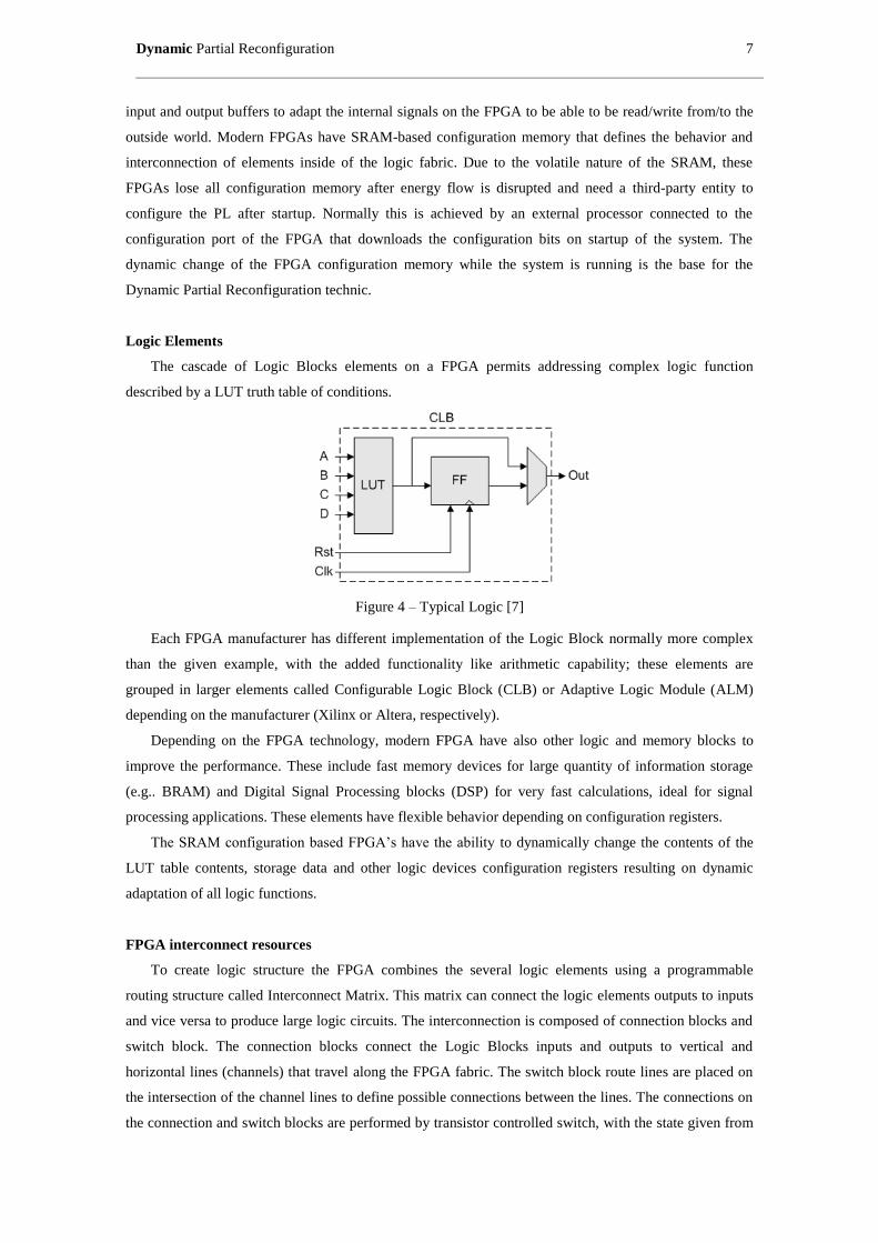
The cascade of Logic Blocks elements on a FPGA permits addressing complex logic function
described by a LUT truth table of conditions.
Figure 4 – Typical Logic [7]
Each FPGA manufacturer has different implementation of the Logic Block normally more complex
than the given example, with the added functionality like arithmetic capability; these elements are
grouped in larger elements called Configurable Logic Block (CLB) or Adaptive Logic Module (ALM)
depending on the manufacturer (Xilinx or Altera, respectively).
Depending on the FPGA technology, modern FPGA have also other logic and memory blocks to
improve the performance. These include fast memory devices for large quantity of information storage
(e.g.. BRAM) and Digital Signal Processing blocks (DSP) for very fast calculations, ideal for signal
processing applications. These elements have flexible behavior depending on configuration registers.
The SRAM configuration based FPGA’s have the ability to dynamically change the contents of the
LUT table contents, storage data and other logic devices configuration registers resulting on dynamic
adaptation of all logic functions.
FPGA interconnect resources
To create logic structure the FPGA combines the several logic elements using a programmable
routing structure called Interconnect Matrix. This matrix can connect the logic elements outputs to inputs
and vice versa to produce large logic circuits. The interconnection is composed of connection blocks and
switch block. The connection blocks connect the Logic Blocks inputs and outputs to vertical and
horizontal lines (channels) that travel along the FPGA fabric. The switch block route lines are placed on
the intersection of the channel lines to define possible connections between the lines. The connections on
the connection and switch blocks are performed by transistor controlled switch, with the state given from
8 Dynamic Partial Reconfiguration
a static RAM (interconnection RAM). The dynamic reconfiguration of the FPGA changes the
interconnection RAM that will trigger changes on the logic block signal routing and thus changing the
logic behavior of the FPGA.
FPGA IO connect resources
The IOBs provide a programmable interface between the internal array of logic blocks and the
device’s external package pins. The IOBs will adapt the internal and external signals so that the internal
logic can communicate with the external environment. These resources are normally programmable to be
able to have different behavior (e.g. behave like a signal input or output). On current FPGA technology
the IOB configuration cannot be dynamic configured. They are configured only by full FPGA
configuration.
FPGA granularity
On commercially available FPGA, the LUT is used as the smallest functional element. To perform
complex functions, a large quantity of these elements have to be implemented on the fabric. The size of
each memory of the LUT will represent a compromise between the area and performance on the FPGA.
The work in [8] and [9], showed that a lookup table size of 4 is the most area efficient in a nonclustered
context. In addition, it was demonstrated in [10] and [11] that using a LUT size of 5 to 6 gave the best
performance.
The FPGA granularity can be described as fine-grained or coarse-grained, depending on the
computation capability of the FPGA. The implementation of a simple structure like a LUT represents a
fine-grained computation capability, on the other end an implementation of large computational blocks,
such as full Arithmetic Logic Units (ALU), represents the coarse-grained. The first is oriented for bit
manipulation logic blocks. The coarse-grained will be more optimal for datapath-oriented computation
that works on standard word sizes (8/16/32 bits).
The commercially available FPGAs use a balanced use of both types of granularity with fine grained
6-LUT architectures with the support of course-grained elements, such as multipliers and memories.
Dynamic Partial Reconfiguration 9
2.2 Dynamic Partial Reconfiguration of FPGA
Dynamic Partial Reconfiguration (DPR) provides a way to modify the implemented logic in FPGA
when the device is on. More clearly DPR allows reconfiguring selected areas of a FPGA while other parts
keep working.
The use of DPR can be seen as the missing link in the gap between a software approach to a problem,
where the system behavior is defined by the running code using the same platform, and an hardware
approach where the flexibility is normally exchanged by the computing power. The use of DPR has also
advantages over conventional designs, including [12]:
- Reducing the size of the FPGA device required to implement a given function, with consequent
reductions in cost and power consumption;
- Providing flexibility in the choices of algorithms or protocols available to an application;
- Enabling new techniques in design security;
- Improving FPGA fault tolerance;
- Accelerating configurable computing.
DPR is not supported on all FPGAs but the new families of Xilinx FPGA normally support DPR. The
Zynq®-7000 family FPGA used in this thesis supports DPR.
2.2.1 Difference-Based Partial Reconfiguration
Partial reconfiguration of an FPGA indicates that a part of the FPGA fabric is reconfigured while the
remaining is not affected on the process. The partial reconfiguration can be applied to a delimited area of
an FPGA, were all logic on that area will be reconfigured between applications on a time multiplexing
scenario. In some approaches the process is based on Difference-Based Partial reconfiguration. The
difference between the two is that the difference-based approach can be used for small design changes
between reconfigurations, especially when the changes on the system are limited to a LUT or Block RAM
contents [13]. In these cases a special a binary file that contains proprietary header information as well as
configuration data – BIT file - can be generated with only the differences between implementations. This
can result in very small BIT files and fast reconfiguration times. The Difference-based approach is out of
the scope of this thesis and will not be further explored.
2.2.2 Dynamic Partial Reconfiguration application examples
The partial reconfiguration of FPGA has been proposed for several applications. This new area of
study is relatively new but a wide range of different application targets can be seen from some of the
examples here described.
Content distribution security
The use of DPR is proposed on the work described in [14]. A system using reconfiguration of the
FPGA could decode protected media data only if the correct partial decoding circuit is configured on a
10 Dynamic Partial Reconfiguration
FPGA. The partial bitstream is stored on a central server and could be downloaded by the client to decode
the media.
Power saving design
Some work has been developed to study the power savings effects on systems that have significant
idle times by using dynamic reconfiguration of FPGA [15, 16] [15, 16] [15, 16]. The FPGA logic is
replaced by a low consuming logic during idle times and overall reductions of power consumption can be
reduced by half [16].
Video processing
Video-based systems are a natural working area for the FPGA architectures. The use of
reconfiguration is essential for system applications that have to deal with different video processing
algorithms. An example of application is the automotive area with the increase demand of driving
auxiliary system that held the driver work by processing the surrounding driving conditions to increase
safety [17].
Fault Tolerant Systems
Application of runtime fault correction strategies for FPGA systems rely on the ability to use
Dynamic Partial Reconfiguration technic as the mean to obtain a fault tolerant system. Modular
Redundancy systems for safety critical applications can also use the DPR to recover from the faulty
conditions. Some study examples of such systems can be found in [18, 19].
Software Defined Radio
The Software Defined Radio refers to a set of techniques that permit the reconfiguration of a
communication system without the need to change a hardware system element. Using these techniques
the communication device can support a wide range of communication standards using the same
hardware platform. A system using FPGA and DPR can be dynamically adapted to work with different
standards with minimum latency and without incurring in service disruption [20].
Dynamic Reconfiguration for Networking Applications
FPGAs have been an important part of several networking projects, some of which use dynamic
reconfiguration.
The Field Programmable Port Extender (FPX) system uses a partially-reconfigurable Xilinx FPGA to
implement a high-speed switch. The FPX system allows packet processing functions to be implemented
as reconfigurable modules. Simplified reconfiguration interfaces in the form of standardized APIs are
used to adapt the modules. Partial bit streams are generated and downloaded into the target FPGA by
sending specialized control packets from remote administration points. Custom tools, such as PARBIT
[7], have been developed to simplify the generation and management of partial bit streams. A
reconfigurable accelerator for packet processing functions in network processors allows customization of
common networking tasks such as tree lookup and pattern matching through partial reconfiguration. The
Dynamic Partial Reconfiguration 11
feasibility of this approach has been demonstrated using a network intrusion detection application. A
dynamically-reconfigurable network processor [8] allows specific parts of a network processor to be
reconfigured to meet the specific workload characteristics.Development System.
For the development of this work an embedded system was used. These systems are normally
computer-based, designed for specific functions with the necessary resources to perform all type of
specific tasks. The systems characteristics of performance, memory, communication resources, power
requirements or very specific control elements are normally associated with the complexity of the task in
hands. Systems tend to have more memory and processing capacity but also more power consumption.
Embedded designers using this type of systems do try to optimize the system without compromising the
result but sometimes the success was only possible with the integration of efficient parallel processing
units and a central controller. The technology evolution and the demand for more flexible systems that
could be ‘adapted’ the needs of the design resulted on hybrid solutions that fusion a processing unit to
programmable logic in a single device.
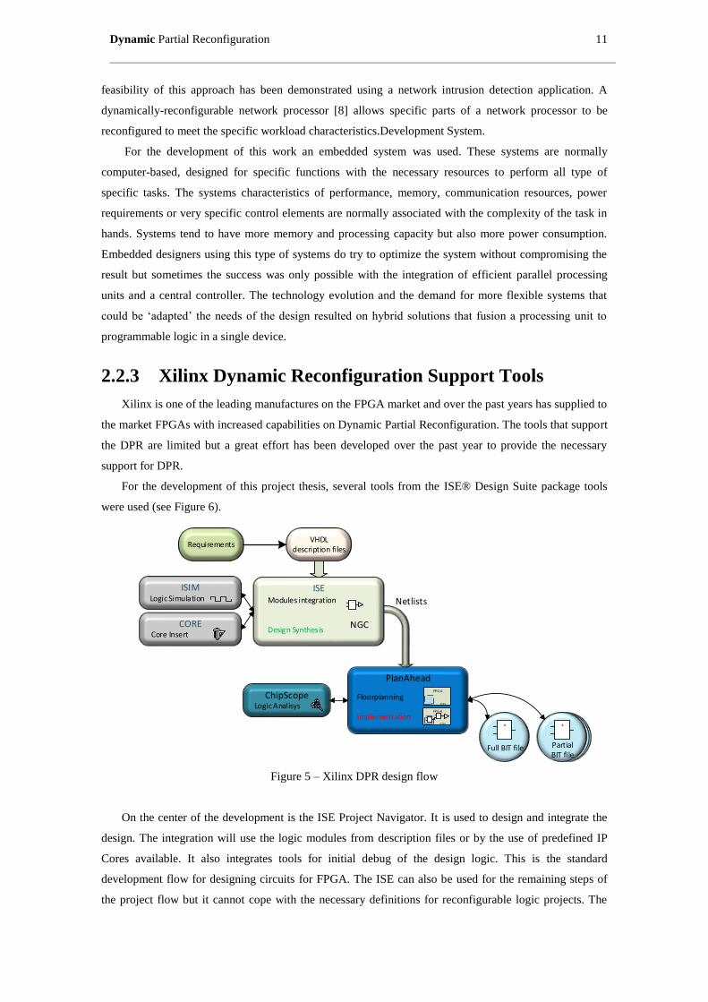
2.2.3 Xilinx Dynamic Reconfiguration Support Tools
Xilinx is one of the leading manufactures on the FPGA market and over the past years has supplied to
the market FPGAs with increased capabilities on Dynamic Partial Reconfiguration. The tools that support
the DPR are limited but a great effort has been developed over the past year to provide the necessary
support for DPR.
For the development of this project thesis, several tools from the ISE® Design Suite package tools
were used (see Figure 6).
ISE
VHDL description files
PlanAhead
Netlists
&0
0
0
Full BIT file
Modules integration
Design Synthesis
>=10
00
NGC
Floorplanning
Implementation >=10
00
FPG A
>=10
00
RP ST ATIC
FPG A
RP ST ATIC
&0
0
0
PartialBIT file
ISIMLogic Simulation
ChipScopeLogic Analisys
CORECore Insert
Requirements
Figure 5 – Xilinx DPR design flow
On the center of the development is the ISE Project Navigator. It is used to design and integrate the
design. The integration will use the logic modules from description files or by the use of predefined IP
Cores available. It also integrates tools for initial debug of the design logic. This is the standard
development flow for designing circuits for FPGA. The ISE can also be used for the remaining steps of
the project flow but it cannot cope with the necessary definitions for reconfigurable logic projects. The
12 Dynamic Partial Reconfiguration
ISE will Synthetize the design and another tool, PlanAhead, will be used for the remaining part of the
project flow, basically the Floorplanning and Implementation. The following steps will be detailed in
continuation.
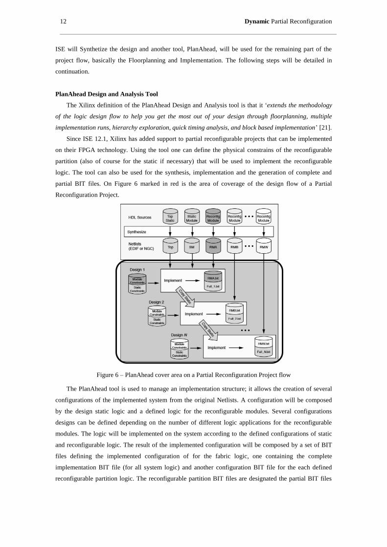
PlanAhead Design and Analysis Tool
The Xilinx definition of the PlanAhead Design and Analysis tool is that it ‘extends the methodology
of the logic design flow to help you get the most out of your design through floorplanning, multiple
implementation runs, hierarchy exploration, quick timing analysis, and block based implementation’ [21].
Since ISE 12.1, Xilinx has added support to partial reconfigurable projects that can be implemented
on their FPGA technology. Using the tool one can define the physical constrains of the reconfigurable
partition (also of course for the static if necessary) that will be used to implement the reconfigurable
logic. The tool can also be used for the synthesis, implementation and the generation of complete and
partial BIT files. On Figure 6 marked in red is the area of coverage of the design flow of a Partial
Reconfiguration Project.
Figure 6 – PlanAhead cover area on a Partial Reconfiguration Project flow
The PlanAhead tool is used to manage an implementation structure; it allows the creation of several
configurations of the implemented system from the original Netlists. A configuration will be composed
by the design static logic and a defined logic for the reconfigurable modules. Several configurations
designs can be defined depending on the number of different logic applications for the reconfigurable
modules. The logic will be implemented on the system according to the defined configurations of static
and reconfigurable logic. The result of the implemented configuration will be composed by a set of BIT
files defining the implemented configuration of for the fabric logic, one containing the complete
implementation BIT file (for all system logic) and another configuration BIT file for the each defined
reconfigurable partition logic. The reconfigurable partition BIT files are designated the partial BIT files
Dynamic Partial Reconfiguration 13
because they only define the system configuration for the reconfigurable partition logic. For the different
designs the static logic will be the same, imported from design to design.
Dynamic Partial Reconfiguration considerations and guidelines
Dynamic Partial Reconfiguration of the FPGA is a powerful technic but subject to several constraints
that must be taken into consideration by the designer. The restrictions and considerations here presented
are oriented for the Xilinx FPGA. Other technology or manufacturer can have different scenarios.
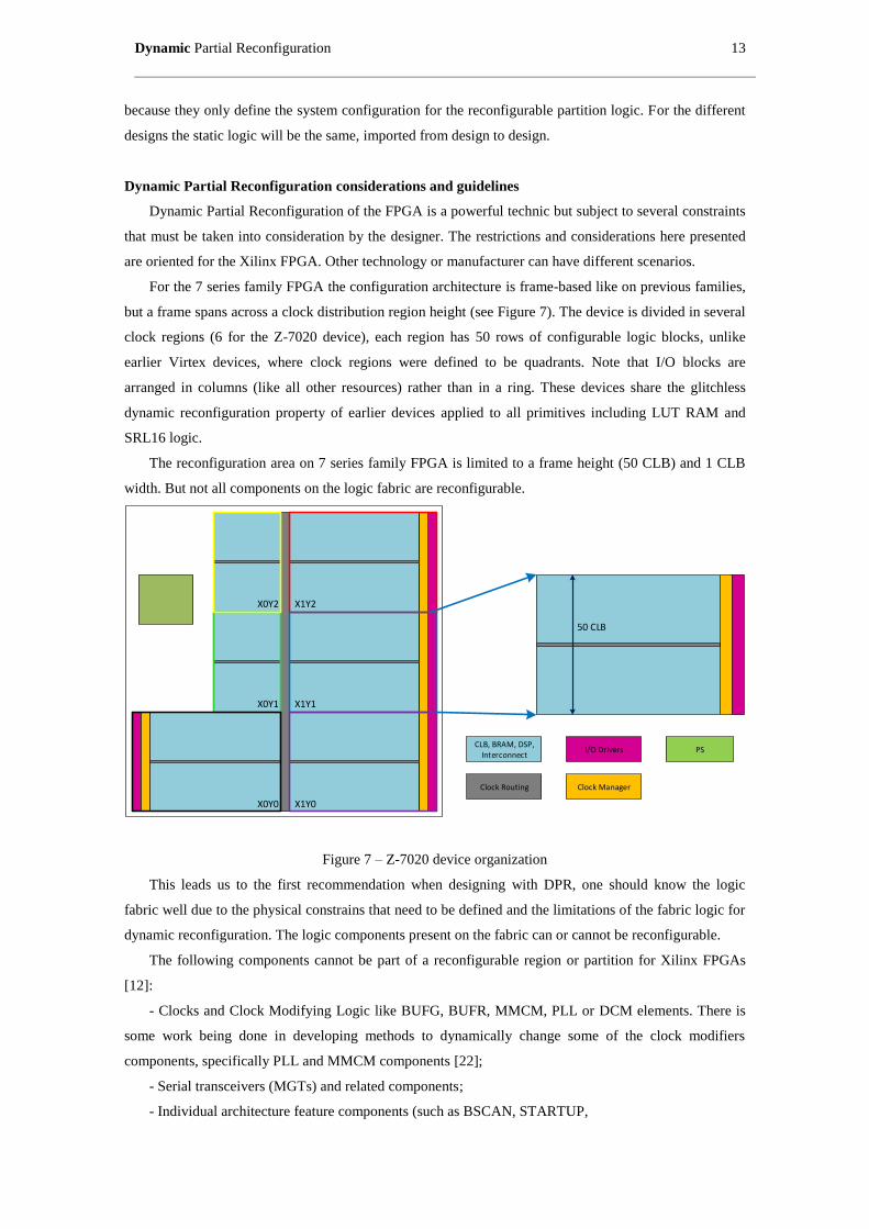
For the 7 series family FPGA the configuration architecture is frame-based like on previous families,
but a frame spans across a clock distribution region height (see Figure 7). The device is divided in several
clock regions (6 for the Z-7020 device), each region has 50 rows of configurable logic blocks, unlike
earlier Virtex devices, where clock regions were defined to be quadrants. Note that I/O blocks are
arranged in columns (like all other resources) rather than in a ring. These devices share the glitchless
dynamic reconfiguration property of earlier devices applied to all primitives including LUT RAM and
SRL16 logic.
The reconfiguration area on 7 series family FPGA is limited to a frame height (50 CLB) and 1 CLB
width. But not all components on the logic fabric are reconfigurable.
X0Y2
X0Y1
X0Y0 X1Y0
X1Y1
X1Y2
50 CLB
CLB, BRAM, DSP, Interconnect
Clock Routing
I/O Drivers
Clock Manager
PS
Figure 7 – Z-7020 device organization
This leads us to the first recommendation when designing with DPR, one should know the logic
fabric well due to the physical constrains that need to be defined and the limitations of the fabric logic for
dynamic reconfiguration. The logic components present on the fabric can or cannot be reconfigurable.
The following components cannot be part of a reconfigurable region or partition for Xilinx FPGAs
[12]:
- Clocks and Clock Modifying Logic like BUFG, BUFR, MMCM, PLL or DCM elements. There is
some work being done in developing methods to dynamically change some of the clock modifiers
components, specifically PLL and MMCM components [22];
- Serial transceivers (MGTs) and related components;
- Individual architecture feature components (such as BSCAN, STARTUP,
14 Dynamic Partial Reconfiguration
XADC, etc.).
Components that can be on the reconfigurable partition:
- All logic block (CLB) components, LUT, flip-flop, register and arithmetic logic;
- I/O and I/O related components are possible to be used on reconfigurable partition but are not
recommended;
- Block RAM. Depending on the FPGA technology some considerations have to be attended, for
instance the 7-series FPGA RAMB36 can be configured has two RAMB18, but only a RAMB36
can be used for the reconfigurable partition even if the logic only uses a RAMB18;
- Digital Signal Processing block (DSP). Also for the 7-series FPGA, for the reconfigurable
partitions these components must be used in groups of 2 DSP48.
Clocking resources
For the reconfigurable project design, other considerations have to be accounted for. For instance the
FPGA global clocking resources used on the FPGA are limited and will depend on the static logic but
also on the Reconfigurable logic. The resources will depend on the device and on the clock regions
occupied by the Reconfigurable Partitions.
Reuse of existing cores
The use of an IP can be restricted on a reconfigurable implementation. For example, the ChipScope
ICON can implement BUFG components (depending on configuration) [23] that cannot be used for
Reconfigurable Partitions. Before using IP cores there must be a study on the necessary resources.
Reset after reconfiguration
The reconfiguration of a used part of the fabric will affect the interconnections, local LUT memory
and BRAM state but once the logic is activated there is no way to predict the possible state of the logic
due to the prior values of the several component outputs. The only way to correctly predict the state of the
logic is to ensure a reset to a defined state of all logic after the reconfiguration is finished. This can be
done by the user logic that can be activated once the reconfigurable partition is updated or in the case of
some Xilinx FPGAs a feature that can be activated by the use of a
RESET_AFTER_RECONFIGURATION flag that will held the reconfigurable region in a steady state
during the reconfiguration process.
Interface Decoupling
The signals that pass between the reconfigurable partition and the static logic have to be decoupled to
avoid strange behavior of the logic. The signals behavior can be erratic and can affect the static logic in a
way that can corrupt memory areas, logic states, I/O and connected components.
The static logic should implement a decoupling of signals to/from the reconfigurable partition by
disabling these interfaces during reconfiguration. In the case of inputs to the reconfigurable modules,
Dynamic Partial Reconfiguration 15
clock and other inputs should be decoupled to prevent spurious writes to memories during
reconfiguration.
The static logic should implement a way to decouple some or all outputs from the reconfigurable
partition during reconfiguration. This is especially critical to Write Enable signals that can affect
memories or other components on the static region in an unpredictable way.
Also, no bidirectional interfaces are permitted between static and reconfigurable regions except in
special dedicated routes.
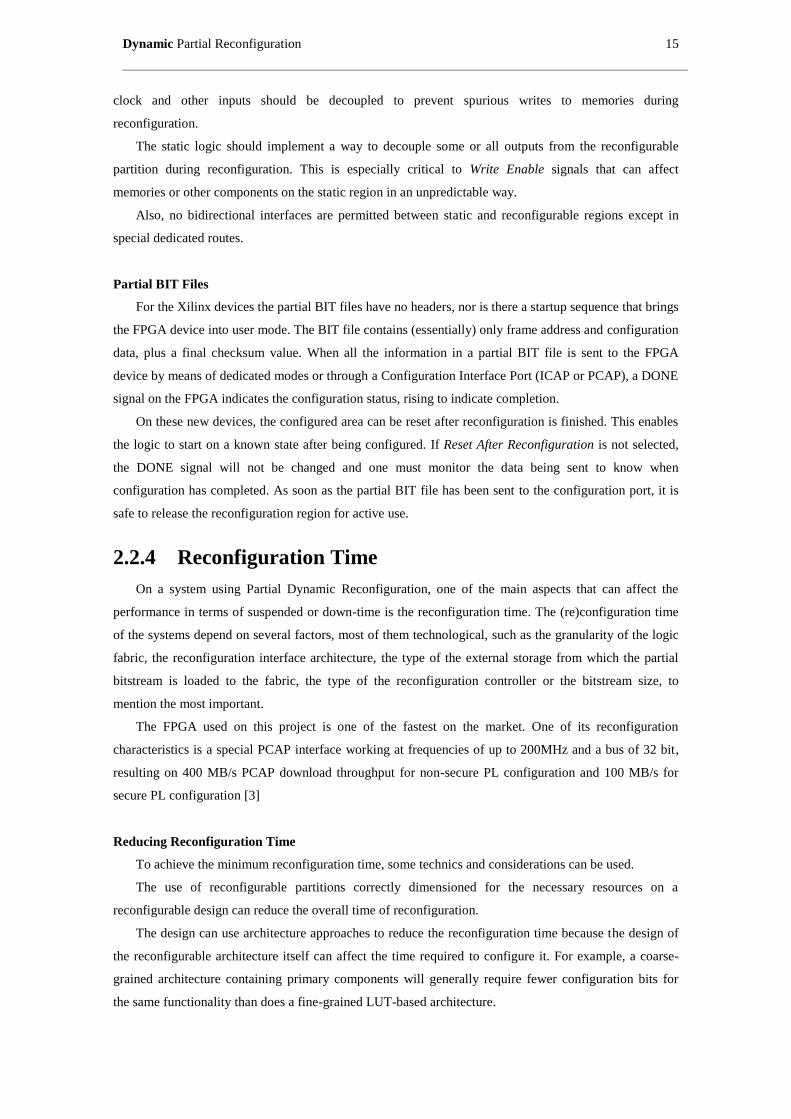
Partial BIT Files
For the Xilinx devices the partial BIT files have no headers, nor is there a startup sequence that brings
the FPGA device into user mode. The BIT file contains (essentially) only frame address and configuration
data, plus a final checksum value. When all the information in a partial BIT file is sent to the FPGA
device by means of dedicated modes or through a Configuration Interface Port (ICAP or PCAP), a DONE
signal on the FPGA indicates the configuration status, rising to indicate completion.
On these new devices, the configured area can be reset after reconfiguration is finished. This enables
the logic to start on a known state after being configured. If Reset After Reconfiguration is not selected,
the DONE signal will not be changed and one must monitor the data being sent to know when
configuration has completed. As soon as the partial BIT file has been sent to the configuration port, it is
safe to release the reconfiguration region for active use.
2.2.4 Reconfiguration Time
On a system using Partial Dynamic Reconfiguration, one of the main aspects that can affect the
performance in terms of suspended or down-time is the reconfiguration time. The (re)configuration time
of the systems depend on several factors, most of them technological, such as the granularity of the logic
fabric, the reconfiguration interface architecture, the type of the external storage from which the partial
bitstream is loaded to the fabric, the type of the reconfiguration controller or the bitstream size, to
mention the most important.
The FPGA used on this project is one of the fastest on the market. One of its reconfiguration
characteristics is a special PCAP interface working at frequencies of up to 200MHz and a bus of 32 bit,
resulting on 400 MB/s PCAP download throughput for non-secure PL configuration and 100 MB/s for
secure PL configuration [3]
Reducing Reconfiguration Time
To achieve the minimum reconfiguration time, some technics and considerations can be used.
The use of reconfigurable partitions correctly dimensioned for the necessary resources on a
reconfigurable design can reduce the overall time of reconfiguration.
The design can use architecture approaches to reduce the reconfiguration time because the design of
the reconfigurable architecture itself can affect the time required to configure it. For example, a coarse-
grained architecture containing primary components will generally require fewer configuration bits for
the same functionality than does a fine-grained LUT-based architecture.
16 Dynamic Partial Reconfiguration
Compression technics on the bitstream data can reduce the amount of configuration data transmitted
to reconfigurable hardware, leading to a corresponding decrease in reconfiguration time. As an example,
the Xilinx 6200 series FPGA includes two “wildcard registers,” equal in bit width to the row and column
addresses, which act as masks on the configuration addresses. This allows one piece of configuration data
to be written to more than one location. Essentially, 0s in the wildcard register retain the configuration
address bits for those locations, whereas 1s indicate that all possible combinations of values in those
specific locations should be addressed. By treating wildcard register value generation as a logic
minimization problem, configuration data is compressed by an average factor of four for the Xilinx 6200
[24] [24].
Xilinx now supports compression technic of BIT file on the BitGen, by minimizing the repeated
frame structures on the configuration information and thus allowing for faster reconfiguration times.
Configuration Security
The increasing use of FPGA on current systems technology means that there is an increasing
potential for intellectual property theft compared to custom ASIC hardware. The SRAM-based FPGAs
have volatile configuration memory. To retain configuration data, a battery must provide a constant
power supply to the configuration memory. This configuration data is stored in memory (RAM or a
PROM) external to the FPGA, and is loaded into the FPGA at system startup. Someone monitoring the
wires between these structures could capture the configuration data flowing from memory to the
reconfigurable device. They could then duplicate the circuit simply by loading that data onto a new chip.
Design firms that create FPGA-based hardware want to protect their work.
Design security can also be provided by encrypting configuration data to obscure the employed
design techniques and/or functionality by implementing on the FPGA hardware capable to decrypt the
AES-GCM, or other encryption algorithms, encrypted bitstream [25]. Now many FPGA vendors include
support for configuration encryption with special on-chip decryption hardware. The Xilinx Zynq-7000
AP SoC devices have the ability to perform a secure boot and to load authenticated and encrypted PS
images and PL bitstreams (full and partial), using a AES/HMAC decryption and authentication engine.
The bitstreams are created using an encryption key that is stored on the device. The encrypted
configurations may only be loaded if they were encrypted with the same key as that stored in the device.
2.2.5 PL Reconfiguration on Zynq®-7000 AP SoC
Previous FPGA architectures allowed the on-chip processor to reconfigure the programmable part of
the PL. This was facilitated by instantiation of an ICAP IP core in the programmable part (the
programmable part needed to be configured before the processor could perform further reconfiguration).
Zynq®-7000 AP SoC has a new feature called processor configuration access port or PCAP which is
part of the PS, and in contrary to ICAP, does not need any instantiation in the PL part. The PS can boot
up and later through PCAP configure the programmable part. The PCAP supports up to 400 megabytes
per second download throughput for non-secure PL configuration bit stream. This can be performed by
DMA transfer, therefore the PS is free during the configuration. Partial reconfiguration is possible and
Dynamic Partial Reconfiguration 17
configuration data is downloaded only for some of the frames and the remaining part of the FPGA not
belonging to configured frames remains unchanged.
The Zynq®-7000 AP SoC PL is based on the Artix-7 and Kintex-7 FPGAs architectures so the
configuration memory is arranged in configuration frames (CF). The frames are the smallest addressable
part of the configuration memory space. The reconfiguration area will be limited to the CF size and all
operation will act upon the whole configuration frame. For the 7 series devices all frames have a fixed,
identical length of 3,232 bits (101 32-bit words) [26]. On these devices the CF can be addressed by the
Frame Address Register that is composed of five fields: block type, top/bottom bit, row address, column
address, and minor address. On the BIT file the frame address can be written directly or auto-incremented
at the end of each frame. The size of the BIT file will depend on the number of configuration frames and
the content of frame addresses.
2.2.6 Exercises on Dynamic Reconfiguration
For the familiarization of the reconfiguration technique in FPGA and to experience on the tools and
the development system proposed, the first step was to develop some simple applications that allowed
working on the requirements necessary for a successful project application.
The criteria for the application were:
a. Dynamic logic algorithm change (reconfiguration);
b. The change should only focus on part of the logic (partial reconfiguration);
c. Reconfiguration controlled and realized by the use of internal ARM processor.
A simple application ensuring the points listed above was developed as follows:
Perform a LED 'shifter' where the direction of displacement was altered by changing the logic on the
reconfigurable part of the fabric. Using the LED's included on the Zedboard (8 in total) was thought two
sets of logic, offset to the left and right shift. To ensure that the system would perform with a static logic
part, the shifter would be composed by the logic concerning the direction of displacement
(reconfigurable) and a timer so that the period of displacement was equal to 1 sec. (static part). The logic
for the offset was also designed to use different resources of the FPGA. The offset to the left was thought
to be implemented through the use of Flip-Flop's while the offset to the right would be implemented with
a BRAM.
Another requirement was that the reconfiguration of logic would be selected by a user using a simple
command line interface and controlled by the ARM processor.
2.2.6.1 Development of a LED scrolling shifter
For the implementation of the system defined above the methodology shown in Figure 5 was
followed. All logic was developed using the ISE tool. The static part of the logic was implemented on the
designated delay entity that instantiates a blackbox entity which represents the reconfigurable entity. The
LED scrolling direction left or right is achieved by a single entity named led_sequence that had two
distinct logic files in VHDL. The number of possible configurations of the system will then be:
1. Static logic + Logic for displacement left
2. Static logic + Logic for displacement right
18 Dynamic Partial Reconfiguration
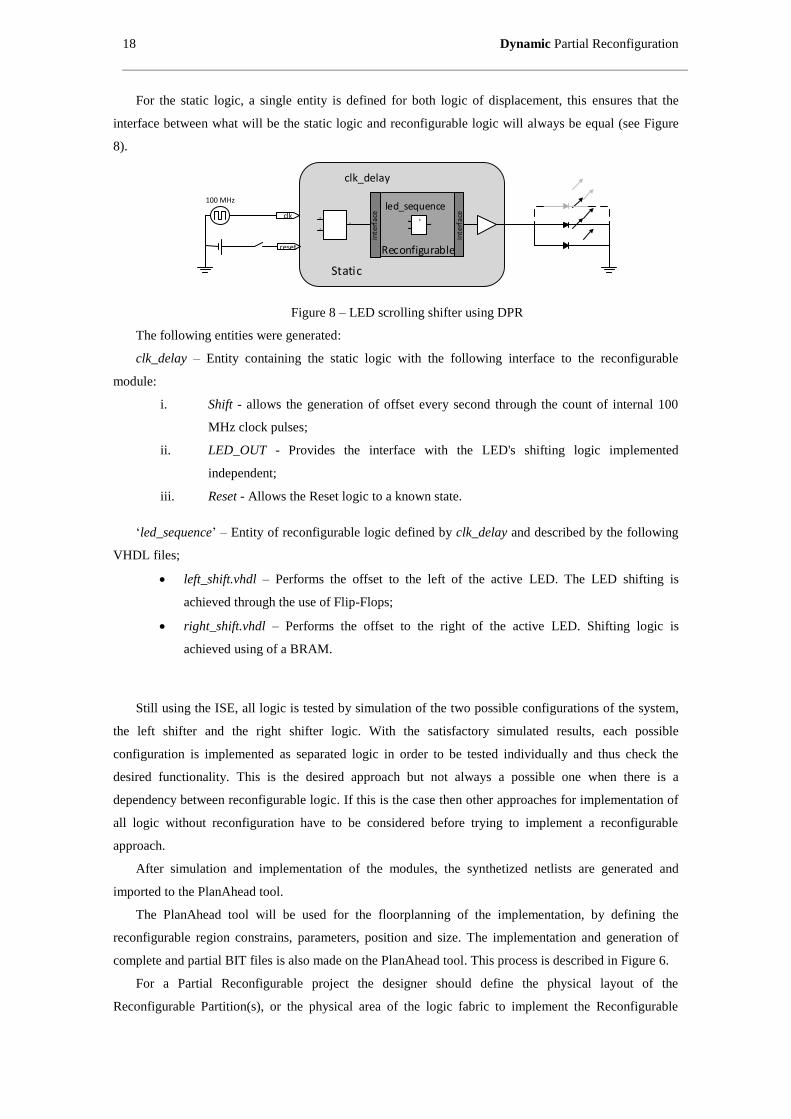
For the static logic, a single entity is defined for both logic of displacement, this ensures that the
interface between what will be the static logic and reconfigurable logic will always be equal (see Figure
8).
&0
0
0
0
0
0
100 MHz
clk_delay
led_sequence
Static
inte
rfa
ce
Reconfigurablereset
inte
rfa
ceclk
Figure 8 – LED scrolling shifter using DPR
The following entities were generated:
clk_delay – Entity containing the static logic with the following interface to the reconfigurable
module:
i. Shift - allows the generation of offset every second through the count of internal 100
MHz clock pulses;
ii. LED_OUT - Provides the interface with the LED's shifting logic implemented
independent;
iii. Reset - Allows the Reset logic to a known state.
‘led_sequence’ – Entity of reconfigurable logic defined by clk_delay and described by the following
VHDL files;
left_shift.vhdl – Performs the offset to the left of the active LED. The LED shifting is
achieved through the use of Flip-Flops;
right_shift.vhdl – Performs the offset to the right of the active LED. Shifting logic is
achieved using of a BRAM.
Still using the ISE, all logic is tested by simulation of the two possible configurations of the system,
the left shifter and the right shifter logic. With the satisfactory simulated results, each possible
configuration is implemented as separated logic in order to be tested individually and thus check the
desired functionality. This is the desired approach but not always a possible one when there is a
dependency between reconfigurable logic. If this is the case then other approaches for implementation of
all logic without reconfiguration have to be considered before trying to implement a reconfigurable
approach.
After simulation and implementation of the modules, the synthetized netlists are generated and
imported to the PlanAhead tool.
The PlanAhead tool will be used for the floorplanning of the implementation, by defining the
reconfigurable region constrains, parameters, position and size. The implementation and generation of
complete and partial BIT files is also made on the PlanAhead tool. This process is described in Figure 6.
For a Partial Reconfigurable project the designer should define the physical layout of the
Reconfigurable Partition(s), or the physical area of the logic fabric to implement the Reconfigurable
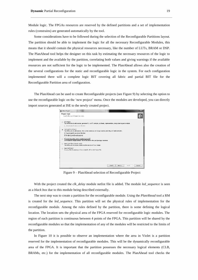
Dynamic Partial Reconfiguration 19
Module logic. The FPGAs resources are reserved by the defined partitions and a set of implementation
rules (constrains) are generated automatically by the tool.
Some considerations have to be followed during the selection of the Reconfigurable Partitions layout.
The partition should be able to implement the logic for all the necessary Reconfigurable Modules, this
means that it should contain the physical resources necessary, like the number of LUTs, BRAM or DSP.
The PlanAhead tool helps the designer on this task by estimating the necessary resources of the logic to
implement and the available by the partition, correlating both values and giving warnings if the available
resources are not sufficient for the logic to be implemented. The PlanAhead allows also the creation of
the several configurations for the static and reconfigurable logic in the system. For each configuration
implemented there will a complete logic BIT covering all fabric and partial BIT file for the
Reconfigurable Partition area of configuration.
The PlanAhead can be used to create Reconfigurable projects (see Figure 9) by selecting the option to
use the reconfigurable logic on the ‘new project’ menu. Once the modules are developed, you can directly
import sources generated at ISE to the newly created project.
Figure 9 – PlanAhead selection of Reconfigurable Project
With the project created the clk_delay module netlist file is added. The module led_sequence is seen
as a black box due to this module being described externally.
The next step was to create a partition for the reconfigurable module. Using the PlanAhead tool a RM
is created for the led_sequence. This partition will set the physical rules of implementation for the
reconfigurable module. Among the rules defined by the partition, there is some defining the logical
location. The location sets the physical area of the FPGA reserved for reconfigurable logic modules. The
region of each partition is continuous between 4 points of the FPGA. This partition will be shared by the
reconfigurable modules so that the implementation of any of the modules will be restricted to the limits of
the partition.
In Figure 10 it is possible to observe an implementation where the area in Violet is a partition
reserved for the implementation of reconfigurable modules. This will be the dynamically reconfigurable
area of the FPGA. It is important that the partition possesses the necessary logical elements (CLB,
BRAMs, etc.) for the implementation of all reconfigurable modules. The PlanAhead tool checks the
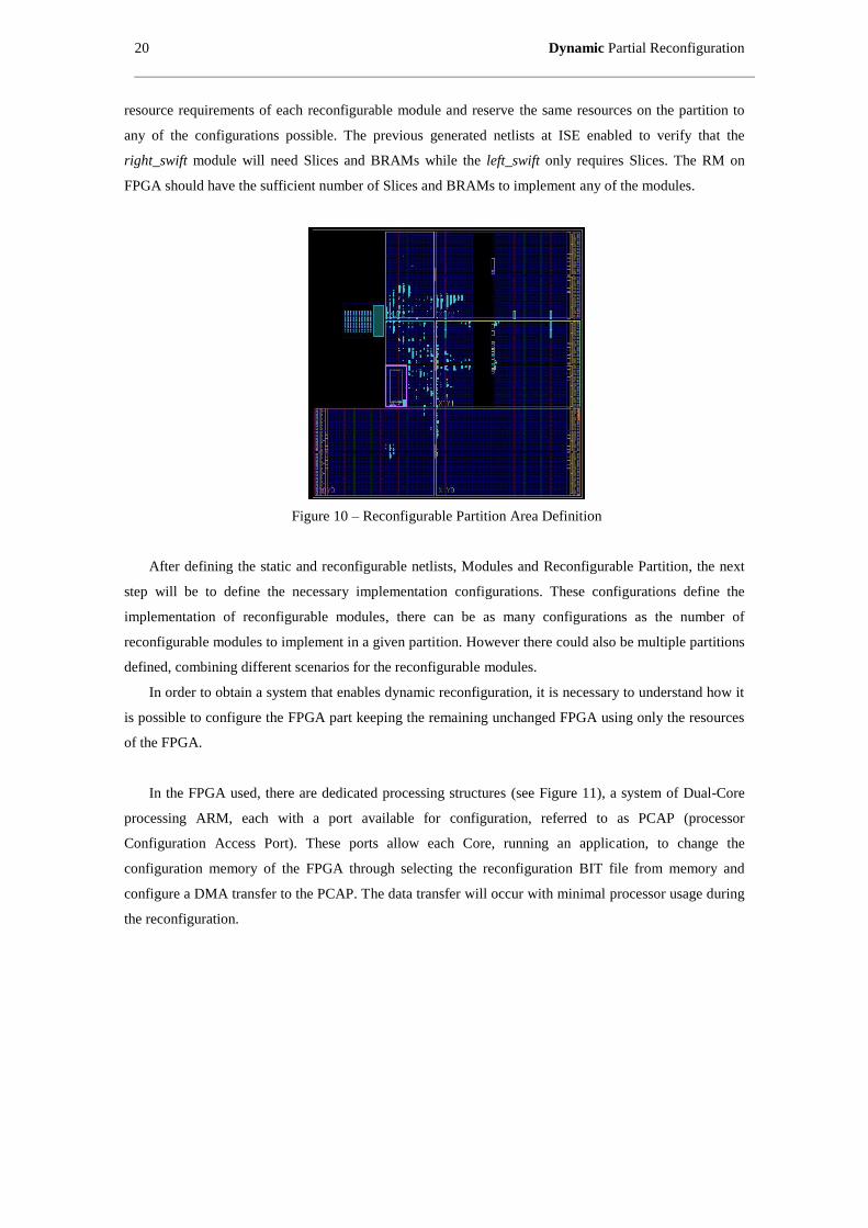
20 Dynamic Partial Reconfiguration
resource requirements of each reconfigurable module and reserve the same resources on the partition to
any of the configurations possible. The previous generated netlists at ISE enabled to verify that the
right_swift module will need Slices and BRAMs while the left_swift only requires Slices. The RM on
FPGA should have the sufficient number of Slices and BRAMs to implement any of the modules.
Figure 10 – Reconfigurable Partition Area Definition
After defining the static and reconfigurable netlists, Modules and Reconfigurable Partition, the next
step will be to define the necessary implementation configurations. These configurations define the
implementation of reconfigurable modules, there can be as many configurations as the number of
reconfigurable modules to implement in a given partition. However there could also be multiple partitions
defined, combining different scenarios for the reconfigurable modules.
In order to obtain a system that enables dynamic reconfiguration, it is necessary to understand how it
is possible to configure the FPGA part keeping the remaining unchanged FPGA using only the resources
of the FPGA.
In the FPGA used, there are dedicated processing structures (see Figure 11), a system of Dual-Core
processing ARM, each with a port available for configuration, referred to as PCAP (processor
Configuration Access Port). These ports allow each Core, running an application, to change the
configuration memory of the FPGA through selecting the reconfiguration BIT file from memory and
configure a DMA transfer to the PCAP. The data transfer will occur with minimal processor usage during
the reconfiguration.
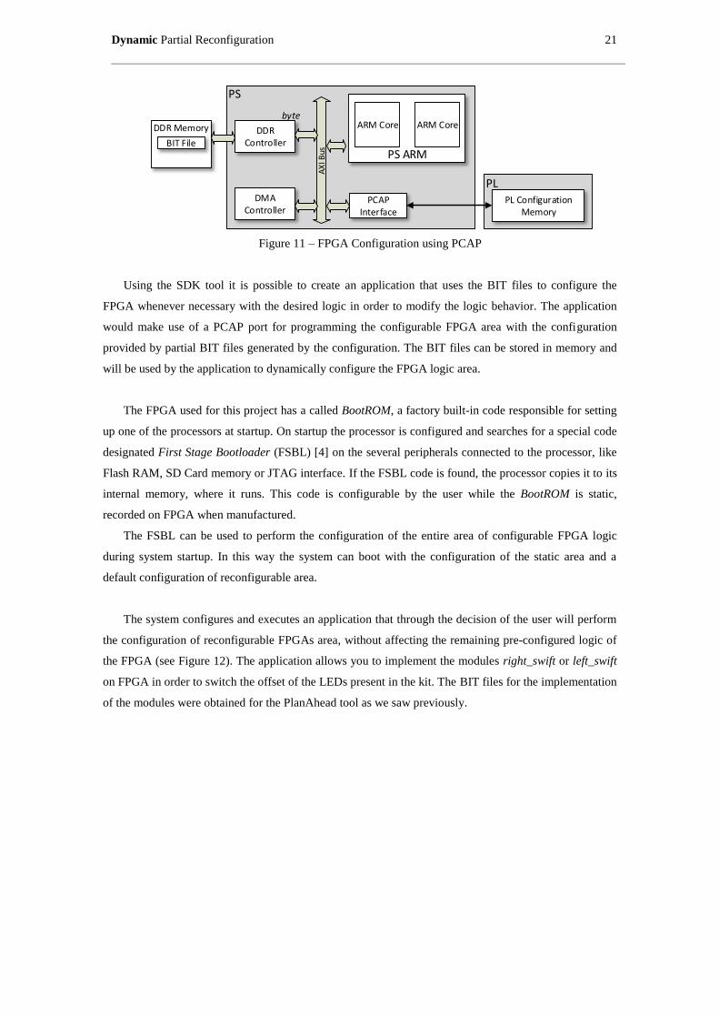
Dynamic Partial Reconfiguration 21
PL
PS
PS ARM
DDR Controller
byte
PL Configuration Memory
ARM Core
PCAP Interface
ARM Core
AX
I Bus
DMA Controller
DDR Memory
BIT File
Figure 11 – FPGA Configuration using PCAP
Using the SDK tool it is possible to create an application that uses the BIT files to configure the
FPGA whenever necessary with the desired logic in order to modify the logic behavior. The application
would make use of a PCAP port for programming the configurable FPGA area with the configuration
provided by partial BIT files generated by the configuration. The BIT files can be stored in memory and
will be used by the application to dynamically configure the FPGA logic area.
The FPGA used for this project has a called BootROM, a factory built-in code responsible for setting
up one of the processors at startup. On startup the processor is configured and searches for a special code
designated First Stage Bootloader (FSBL) [4] on the several peripherals connected to the processor, like
Flash RAM, SD Card memory or JTAG interface. If the FSBL code is found, the processor copies it to its
internal memory, where it runs. This code is configurable by the user while the BootROM is static,
recorded on FPGA when manufactured.
The FSBL can be used to perform the configuration of the entire area of configurable FPGA logic
during system startup. In this way the system can boot with the configuration of the static area and a
default configuration of reconfigurable area.
The system configures and executes an application that through the decision of the user will perform
the configuration of reconfigurable FPGAs area, without affecting the remaining pre-configured logic of
the FPGA (see Figure 12). The application allows you to implement the modules right_swift or left_swift
on FPGA in order to switch the offset of the LEDs present in the kit. The BIT files for the implementation
of the modules were obtained for the PlanAhead tool as we saw previously.
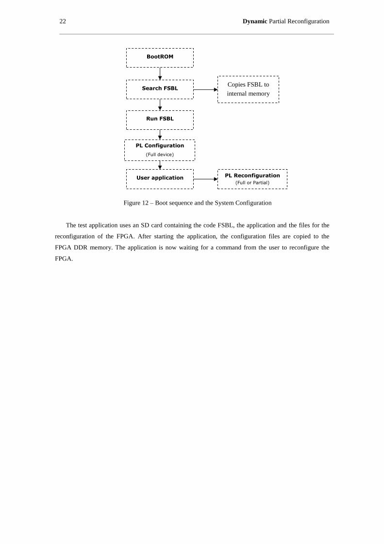
22 Dynamic Partial Reconfiguration
Figure 12 – Boot sequence and the System Configuration
The test application uses an SD card containing the code FSBL, the application and the files for the
reconfiguration of the FPGA. After starting the application, the configuration files are copied to the
FPGA DDR memory. The application is now waiting for a command from the user to reconfigure the
FPGA.
BootROM
Copies FSBL to
internal memory Search FSBL
Run FSBL
PL Configuration
(Full device)
User application PL Reconfiguration
(Full or Partial)
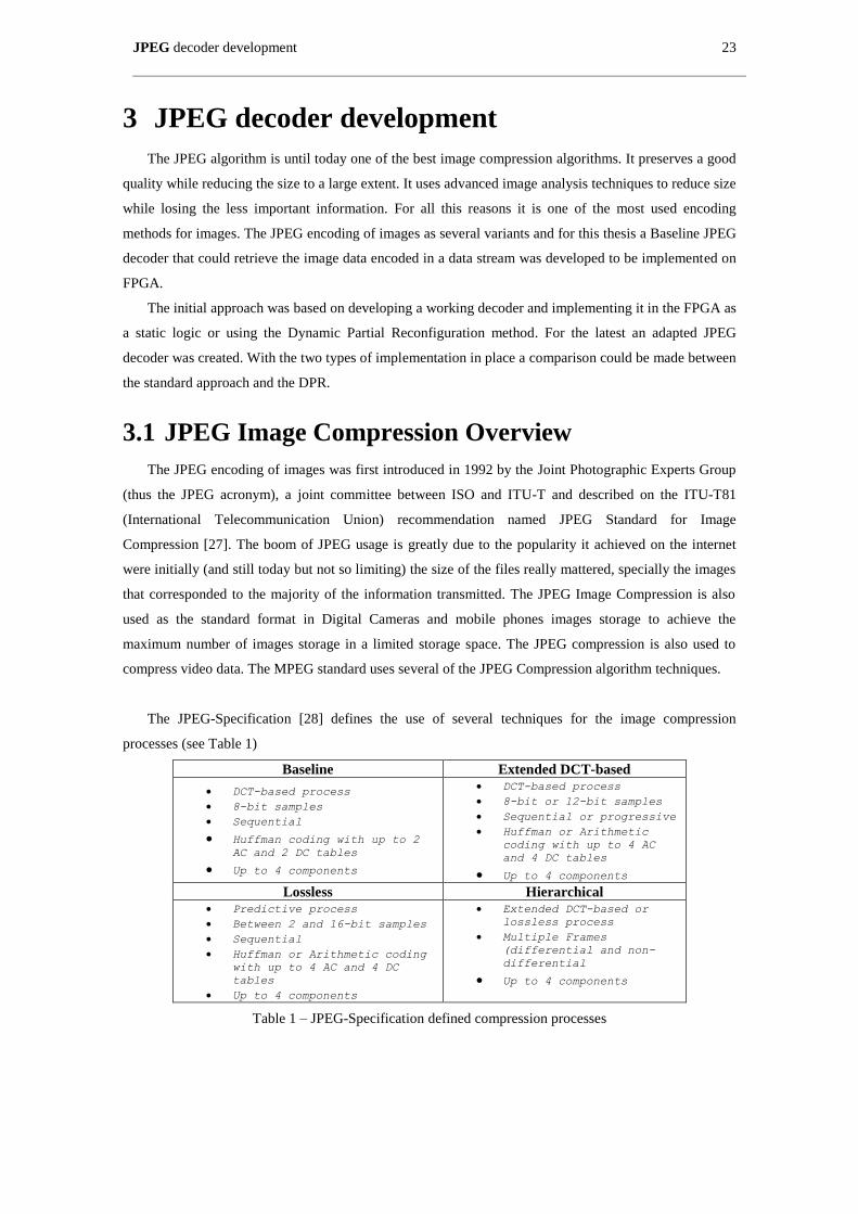
JPEG decoder development 23
3 JPEG decoder development
The JPEG algorithm is until today one of the best image compression algorithms. It preserves a good
quality while reducing the size to a large extent. It uses advanced image analysis techniques to reduce size
while losing the less important information. For all this reasons it is one of the most used encoding
methods for images. The JPEG encoding of images as several variants and for this thesis a Baseline JPEG
decoder that could retrieve the image data encoded in a data stream was developed to be implemented on
FPGA.
The initial approach was based on developing a working decoder and implementing it in the FPGA as
a static logic or using the Dynamic Partial Reconfiguration method. For the latest an adapted JPEG
decoder was created. With the two types of implementation in place a comparison could be made between
the standard approach and the DPR.
3.1 JPEG Image Compression Overview
The JPEG encoding of images was first introduced in 1992 by the Joint Photographic Experts Group
(thus the JPEG acronym), a joint committee between ISO and ITU-T and described on the ITU-T81
(International Telecommunication Union) recommendation named JPEG Standard for Image
Compression [27]. The boom of JPEG usage is greatly due to the popularity it achieved on the internet
were initially (and still today but not so limiting) the size of the files really mattered, specially the images
that corresponded to the majority of the information transmitted. The JPEG Image Compression is also
used as the standard format in Digital Cameras and mobile phones images storage to achieve the
maximum number of images storage in a limited storage space. The JPEG compression is also used to
compress video data. The MPEG standard uses several of the JPEG Compression algorithm techniques.
The JPEG-Specification [28] defines the use of several techniques for the image compression
processes (see Table 1)
Baseline Extended DCT-based
DCT-based process
8-bit samples
Sequential
Huffman coding with up to 2
AC and 2 DC tables
Up to 4 components
DCT-based process
8-bit or 12-bit samples
Sequential or progressive
Huffman or Arithmetic
coding with up to 4 AC
and 4 DC tables
Up to 4 components
Lossless Hierarchical Predictive process
Between 2 and 16-bit samples
Sequential
Huffman or Arithmetic coding
with up to 4 AC and 4 DC
tables
Up to 4 components
Extended DCT-based or
lossless process
Multiple Frames
(differential and non-
differential
Up to 4 components
Table 1 – JPEG-Specification defined compression processes
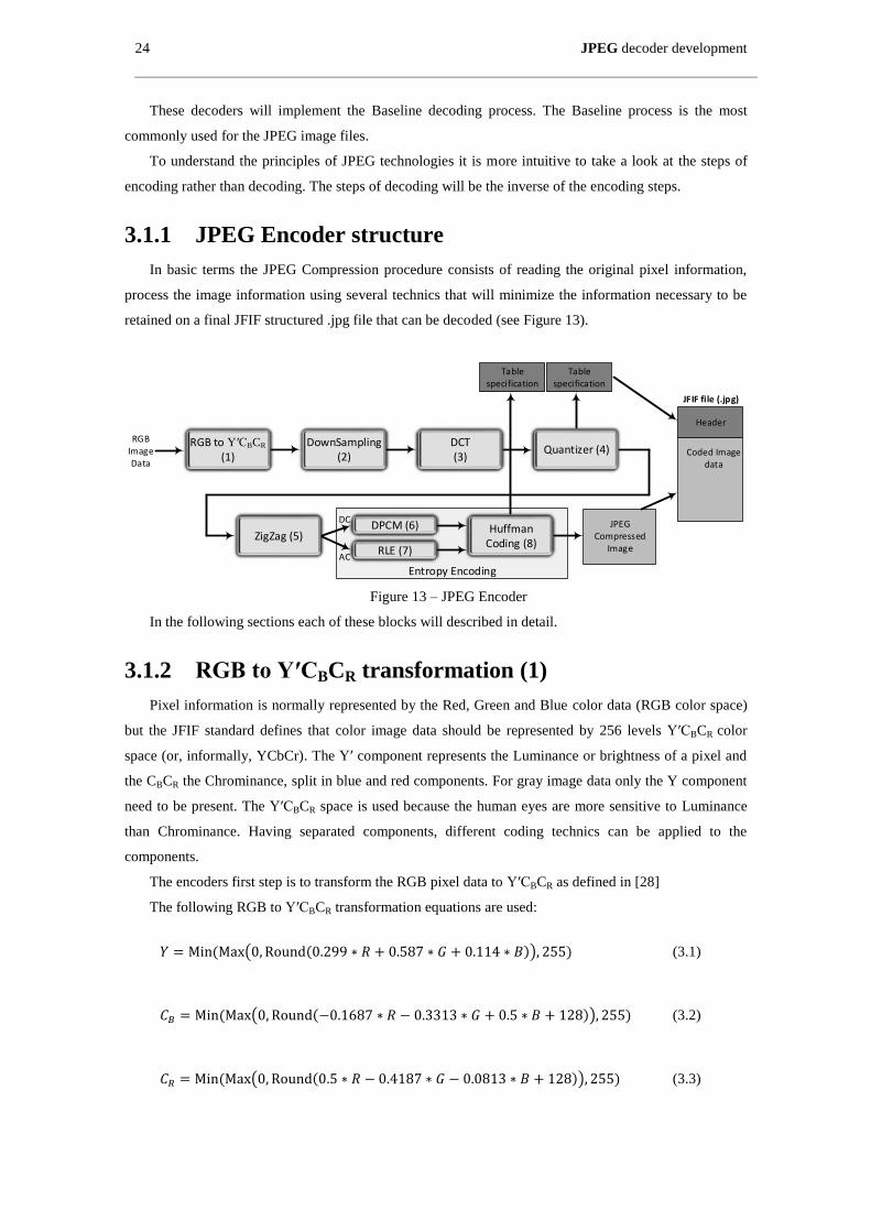
24 JPEG decoder development
These decoders will implement the Baseline decoding process. The Baseline process is the most
commonly used for the JPEG image files.
To understand the principles of JPEG technologies it is more intuitive to take a look at the steps of
encoding rather than decoding. The steps of decoding will be the inverse of the encoding steps.
3.1.1 JPEG Encoder structure
In basic terms the JPEG Compression procedure consists of reading the original pixel information,
process the image information using several technics that will minimize the information necessary to be
retained on a final JFIF structured .jpg file that can be decoded (see Figure 13).
Entropy Encoding
RGB to Y′CBCR
(1)
RGB Image Data
DownSampling(2)
DCT(3)
HuffmanCoding (8)
JPEG Compressed
Image
Quantizer (4)
Table specification
Table specification
ZigZag (5)DPCM (6)
RLE (7)
JFIF file (.jpg)
Header
Coded Image data
DC
AC
Figure 13 – JPEG Encoder
In the following sections each of these blocks will described in detail.
3.1.2 RGB to Y′CBCR transformation (1)
Pixel information is normally represented by the Red, Green and Blue color data (RGB color space)
but the JFIF standard defines that color image data should be represented by 256 levels Y′CBCR color
space (or, informally, YCbCr). The Y′ component represents the Luminance or brightness of a pixel and
the CBCR the Chrominance, split in blue and red components. For gray image data only the Y component
need to be present. The Y′CBCR space is used because the human eyes are more sensitive to Luminance
than Chrominance. Having separated components, different coding technics can be applied to the
components.
The encoders first step is to transform the RGB pixel data to Y′CBCR as defined in [28]
The following RGB to Y′CBCR transformation equations are used:
( )) ) (3.1)
( )) ) (3.2)
( )) ) (3.3)
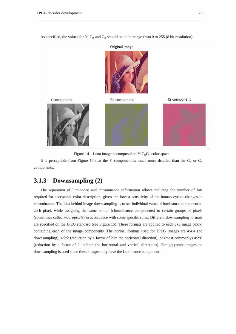
JPEG decoder development 25
As specified, the values for Y, CB and CR should be in the range from 0 to 255 (8 bit resolution).
Figure 14 – Lena image decomposed to Y’CBCR color space
It is perceptible from Figure 14 that the Y component is much more detailed than the CB or CR
components.
3.1.3 Downsampling (2)
The separation of luminance and chrominance information allows reducing the number of bits
required for acceptable color description, given the lowest sensitivity of the human eye to changes in
chrominance. The idea behind image downsampling is to set individual value of luminance component to
each pixel, while assigning the same colour (chrominance components) to certain groups of pixels
(sometimes called macropixels) in accordance with some specific rules. Different downsampling formats
are specified on the JPEG standard (see Figure 15). These formats are applied to each 8x8 image block,
containing each of the image components. The normal formats used for JPEG images are 4:4:4 (no
downsampling), 4:2:2 (reduction by a factor of 2 in the horizontal direction), or (most commonly) 4:2:0
(reduction by a factor of 2 in both the horizontal and vertical directions). For grayscale images no
downsampling is used since these images only have the Luminance component.
Original image
Y component Cb component Cr component
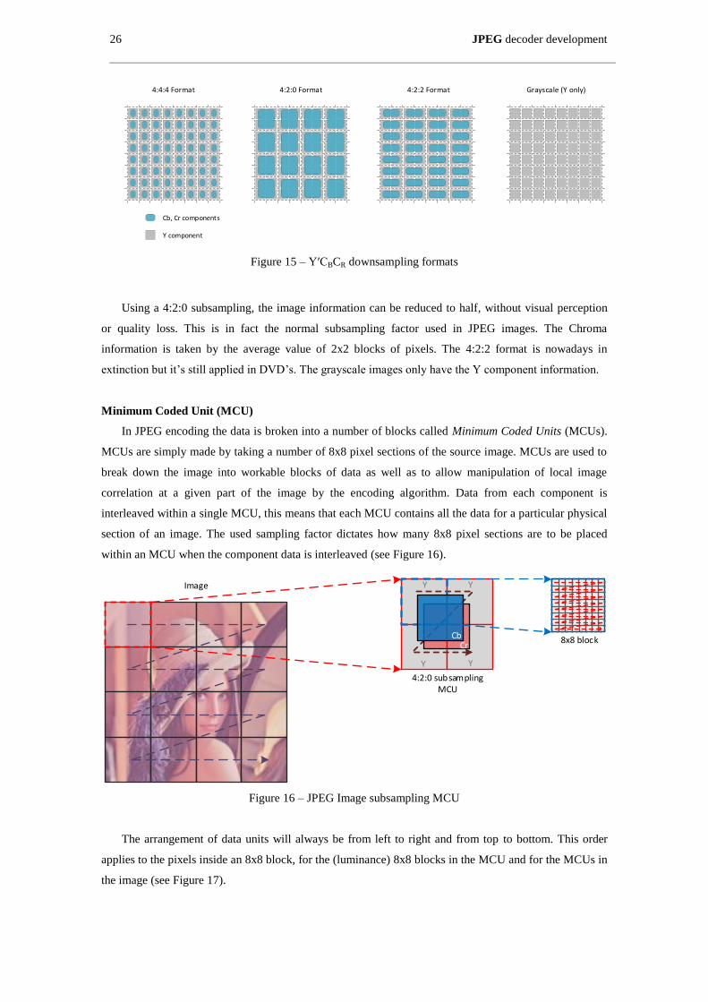
26 JPEG decoder development
Cb, Cr components
Y component
4:4:4 Format 4:2:0 Format 4:2:2 Format Grayscale (Y only)
Figure 15 – Y′CBCR downsampling formats
Using a 4:2:0 subsampling, the image information can be reduced to half, without visual perception
or quality loss. This is in fact the normal subsampling factor used in JPEG images. The Chroma
information is taken by the average value of 2x2 blocks of pixels. The 4:2:2 format is nowadays in
extinction but it’s still applied in DVD’s. The grayscale images only have the Y component information.
Minimum Coded Unit (MCU)
In JPEG encoding the data is broken into a number of blocks called Minimum Coded Units (MCUs).
MCUs are simply made by taking a number of 8x8 pixel sections of the source image. MCUs are used to
break down the image into workable blocks of data as well as to allow manipulation of local image
correlation at a given part of the image by the encoding algorithm. Data from each component is
interleaved within a single MCU, this means that each MCU contains all the data for a particular physical
section of an image. The used sampling factor dictates how many 8x8 pixel sections are to be placed
within an MCU when the component data is interleaved (see Figure 16).
8x8 block
4:2:0 subsampling MCU
Image
Y Y
YY
CbCr
Figure 16 – JPEG Image subsampling MCU
The arrangement of data units will always be from left to right and from top to bottom. This order
applies to the pixels inside an 8x8 block, for the (luminance) 8x8 blocks in the MCU and for the MCUs in
the image (see Figure 17).
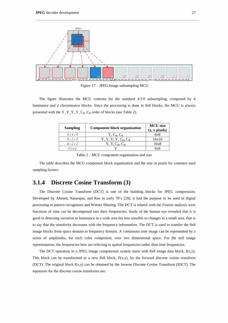
JPEG decoder development 27
Y Y
YY
CbCr
Y Y Y Y Cb Cr Y Y Y Y Cb Cr
MCU 1
MCU 1 MCU 2
Figure 17 – JPEG Image subsampling MCU
The figure illustrates the MCU contents for the standard 4:2:0 subsampling, composed by 4
luminance and 2 chrominance blocks. Since the processing is done in 8x8 blocks, the MCU is always
presented with the Y_Y_Y_Y_CB_CR order of blocks (see Table 2).
Sampling Component block organization MCU size
(x, y pixels)
4:4:4 Y, CB, CR 8x8
4:2:0 Y, Y, Y, Y, CB, CR 16x16
4:2:2 Y, Y, CB, CR 16x8
Gray Y 8x8
Table 2 – MCU component organization and size
The table describes the MCU component block organization and the size in pixels for common used
sampling factors.
3.1.4 Discrete Cosine Transform (3)
The Discrete Cosine Transform (DCT) is one of the building blocks for JPEG compression.
Developed by Ahmed, Natarajan, and Rao in early 70’s [29], it had the purpose to be used in digital
processing in pattern recognition and Wiener filtering. The DCT is related with the Fourier analysis were
functions of time can be decomposed into their frequencies. Study of the human eye revealed that it is
good in detecting variation in luminance in a wide area but less sensible to changes in a small area, that is
to say that the sensitivity decreases with the frequency information. The DCT is used to transfer the 8x8
image blocks from space domain to frequency domain. A continuous tone image can be represented by a
series of amplitudes, for each color component, over two dimensional space. For the still image
representation, the frequencies here are referring to spatial frequencies rather than time frequencies.
The DCT operation in a JPEG image compression system starts with 8x8 image data block, f(x,y).
This block can be transformed to a new 8x8 block, F(x,y), by the forward discrete cosine transform
(DCT). The original block f(x,y) can be obtained by the Inverse Discrete Cosine Transform (IDCT). The
equations for the discrete cosine transforms are:
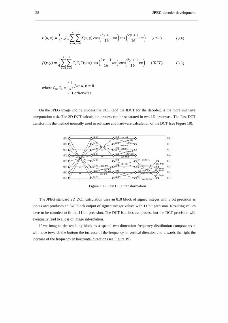
28 JPEG decoder development
)
∑ ∑ ) (
) (
)
) (3.4)
)
∑ ∑ ) (
) (
)
) (3.5)
{
√
On the JPEG image coding process the DCT (and the IDCT for the decoder) is the more intensive
computation task. The 2D DCT calculation process can be separated in two 1D processes. The Fast DCT
transform is the method normally used in software and hardware calculation of the DCT (see Figure 18).
Figure 18 – Fast DCT transformation
The JPEG standard 2D DCT calculation uses an 8x8 block of signed integer with 8 bit precision as
inputs and produces an 8x8 block output of signed integer values with 11 bit precision. Resulting values
have to be rounded to fit the 11 bit precision. The DCT is a lossless process but the DCT precision will
eventually lead to a loss of image information.
If we imagine the resulting block as a spatial two dimension frequency distribution components it
will have towards the bottom the increase of the frequency in vertical direction and towards the right the
increase of the frequency in horizontal direction (see Figure 19).
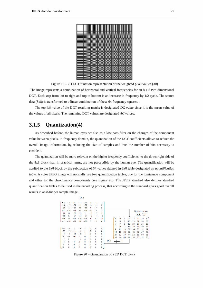
JPEG decoder development 29
Figure 19 – 2D DCT function representation of the weighted pixel values [30]
The image represents a combination of horizontal and vertical frequencies for an 8 x 8 two-dimensional
DCT. Each step from left to right and top to bottom is an increase in frequency by 1/2 cycle. The source
data (8x8) is transformed to a linear combination of these 64 frequency squares.
The top left value of the DCT resulting matrix is designated DC value since it is the mean value of
the values of all pixels. The remaining DCT values are designated AC values.
3.1.5 Quantization(4)
As described before, the human eyes act also as a low pass filter on the changes of the component
value between pixels. In frequency domain, the quantization of the DCT coefficients allows to reduce the
overall image information, by reducing the size of samples and thus the number of bits necessary to
encode it.
The quantization will be more relevant on the higher frequency coefficients, to the down right side of
the 8x8 block that, in practical terms, are not perceptible by the human eye. The quantification will be
applied to the 8x8 block by the subtraction of 64 values defined in 8x8 table designated as quantification
table. A color JPEG image will normally use two quantification tables, one for the luminance component
and other for the chrominance components (see Figure 20). The JPEG standard also defines standard
quantification tables to be used in the encoding process, that according to the standard gives good overall
results in an 8-bit per sample image.
Figure 20 – Quantization of a 2D DCT block
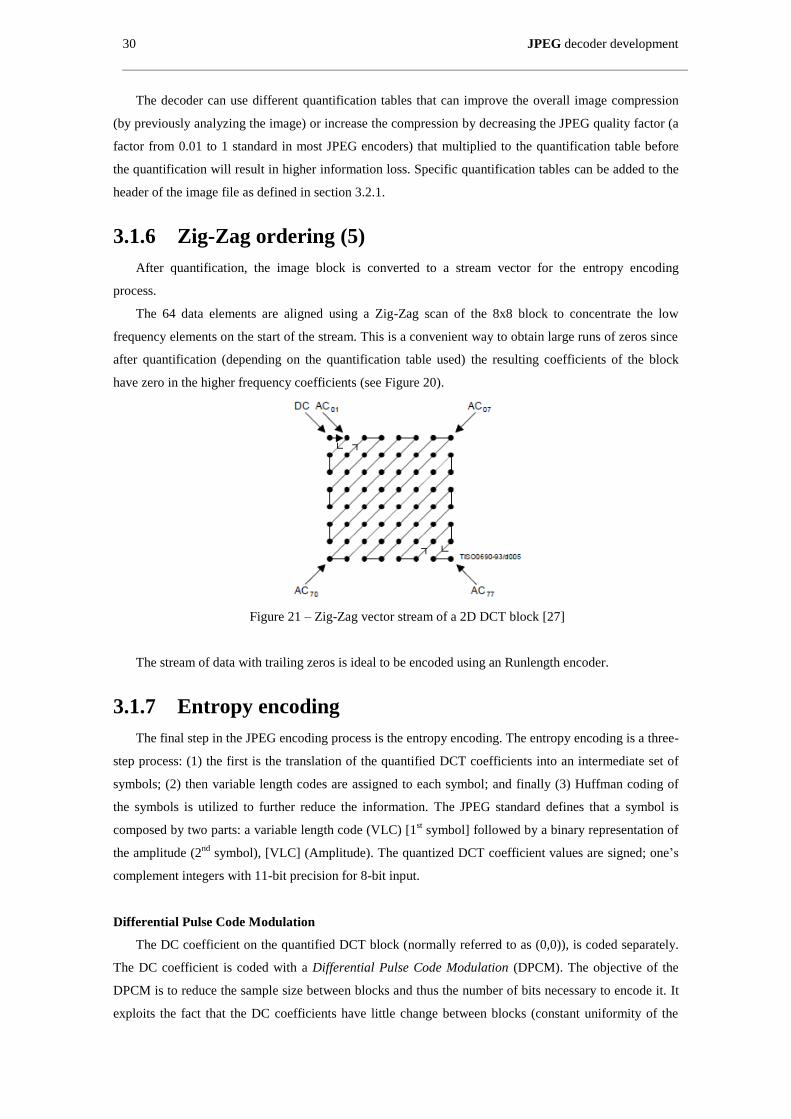
30 JPEG decoder development
The decoder can use different quantification tables that can improve the overall image compression
(by previously analyzing the image) or increase the compression by decreasing the JPEG quality factor (a
factor from 0.01 to 1 standard in most JPEG encoders) that multiplied to the quantification table before
the quantification will result in higher information loss. Specific quantification tables can be added to the
header of the image file as defined in section 3.2.1.
3.1.6 Zig-Zag ordering (5)
After quantification, the image block is converted to a stream vector for the entropy encoding
process.
The 64 data elements are aligned using a Zig-Zag scan of the 8x8 block to concentrate the low
frequency elements on the start of the stream. This is a convenient way to obtain large runs of zeros since
after quantification (depending on the quantification table used) the resulting coefficients of the block
have zero in the higher frequency coefficients (see Figure 20).
Figure 21 – Zig-Zag vector stream of a 2D DCT block [27]
The stream of data with trailing zeros is ideal to be encoded using an Runlength encoder.
3.1.7 Entropy encoding
The final step in the JPEG encoding process is the entropy encoding. The entropy encoding is a three-
step process: (1) the first is the translation of the quantified DCT coefficients into an intermediate set of
symbols; (2) then variable length codes are assigned to each symbol; and finally (3) Huffman coding of
the symbols is utilized to further reduce the information. The JPEG standard defines that a symbol is
composed by two parts: a variable length code (VLC) [1st symbol] followed by a binary representation of
the amplitude (2nd
symbol), [VLC] (Amplitude). The quantized DCT coefficient values are signed; one’s
complement integers with 11-bit precision for 8-bit input.
Differential Pulse Code Modulation
The DC coefficient on the quantified DCT block (normally referred to as (0,0)), is coded separately.
The DC coefficient is coded with a Differential Pulse Code Modulation (DPCM). The objective of the
DPCM is to reduce the sample size between blocks and thus the number of bits necessary to encode it. It
exploits the fact that the DC coefficients have little change between blocks (constant uniformity of the
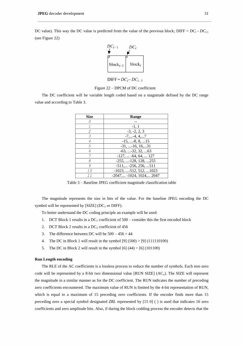
JPEG decoder development 31
DC value). This way the DC value is predicted from the value of the previous block; DIFF = DCi - DCi-1
(see Figure 22)
Figure 22 – DPCM of DC coefficient
The DC coefficient will be variable length coded based on a magnitude defined by the DC range
value and according to Table 3.
Size Range
0 --
1 -1, 1
2 -3, -2, 2, 3
3 -7,...-4, 4,...7
4 -15, ...-8, 8, ...15
5 -31, ...-16, 16,...31
6 -63, ...-32, 32, ...63
7 -127, ... -64, 64, ... 127
8 -255, ...-128, 128, ...255
9 -511,... -256, 256, ...511
10 -1023, ...-512, 512, ...1023
11 -2047,... -1024, 1024,... 2047
Table 3 – Baseline JPEG coefficient magnitude classification table
The magnitude represents the size in bits of the value. For the baseline JPEG encoding the DC
symbol will be represented by [SIZE] (DC1 or DIFF).
To better understand the DC coding principle an example will be used:
1. DCT Block 1 results in a DC1 coefficient of 500 – consider this the first encoded block
2. DCT Block 2 results in a DC2 coefficient of 456
3. The difference between DC will be 500 – 456 = 44
4. The DC in Block 1 will result in the symbol [9] (500) > [9] (111110100)
5. The DC in Block 2 will result in the symbol [6] (44) > [6] (101100)
Run Length encoding
The RLE of the AC coefficients is a lossless process to reduce the number of symbols. Each non-zero
code will be represented by a 8-bit two dimensional value [RUN SIZE] (ACx). The SIZE will represent
the magnitude in a similar manner as for the DC coefficient. The RUN indicates the number of preceding
zero coefficients encountered. The maximum value of RUN is limited by the 4-bit representation of RUN,
which is equal to a maximum of 15 preceding zero coefficients. If the encoder finds more than 15
preceding zero a special symbol designated ZRL represented by [15 0] ( ) is used that indicates 16 zero
coefficients and zero amplitude bits. Also, if during the block codding process the encoder detects that the
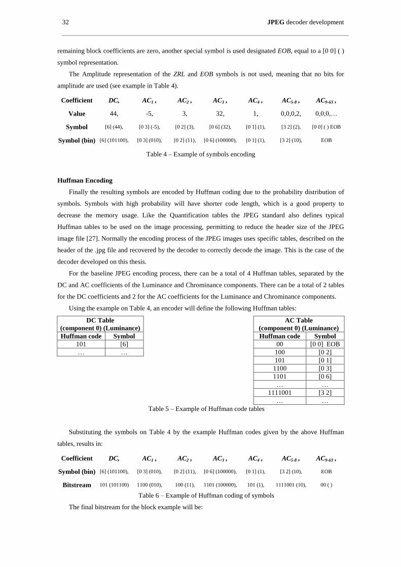
32 JPEG decoder development
remaining block coefficients are zero, another special symbol is used designated EOB, equal to a [0 0] ( )
symbol representation.
The Amplitude representation of the ZRL and EOB symbols is not used, meaning that no bits for
amplitude are used (see example in Table 4).
Coefficient DC, AC1 , AC2 , AC3 , AC4 , AC5-8 , AC9-63 ,
Value 44, -5, 3, 32, 1, 0,0,0,2, 0,0,0,…
Symbol [6] (44), [0 3] (-5), [0 2] (3), [0 6] (32), [0 1] (1), [3 2] (2), [0 0] ( ) EOB
Symbol (bin) [6] (101100), [0 3] (010), [0 2] (11), [0 6] (100000), [0 1] (1), [3 2] (10), EOB
Table 4 – Example of symbols encoding
Huffman Encoding
Finally the resulting symbols are encoded by Huffman coding due to the probability distribution of
symbols. Symbols with high probability will have shorter code length, which is a good property to
decrease the memory usage. Like the Quantification tables the JPEG standard also defines typical
Huffman tables to be used on the image processing, permitting to reduce the header size of the JPEG
image file [27]. Normally the encoding process of the JPEG images uses specific tables, described on the
header of the .jpg file and recovered by the decoder to correctly decode the image. This is the case of the
decoder developed on this thesis.
For the baseline JPEG encoding process, there can be a total of 4 Huffman tables, separated by the
DC and AC coefficients of the Luminance and Chrominance components. There can be a total of 2 tables
for the DC coefficients and 2 for the AC coefficients for the Luminance and Chrominance components.
Using the example on Table 4, an encoder will define the following Huffman tables:
DC Table
(component 0) (Luminance)
AC Table
(component 0) (Luminance)
Huffman code Symbol Huffman code Symbol
101 [6] 00 [0 0] EOB
… … 100 [0 2]
101 [0 1]
1100 [0 3]
1101 [0 6]
… …
1111001 [3 2]
… …
Table 5 – Example of Huffman code tables
Substituting the symbols on Table 4 by the example Huffman codes given by the above Huffman
tables, results in:
Coefficient DC, AC1 , AC2 , AC3 , AC4 , AC5-8 , AC9-63 ,
Symbol (bin) [6] (101100), [0 3] (010), [0 2] (11), [0 6] (100000), [0 1] (1), [3 2] (10), EOB
Bitstream 101 (101100) 1100 (010), 100 (11), 1101 (100000), 101 (1), 1111001 (10), 00 ( )
Table 6 – Example of Huffman coding of symbols
The final bitstream for the block example will be:
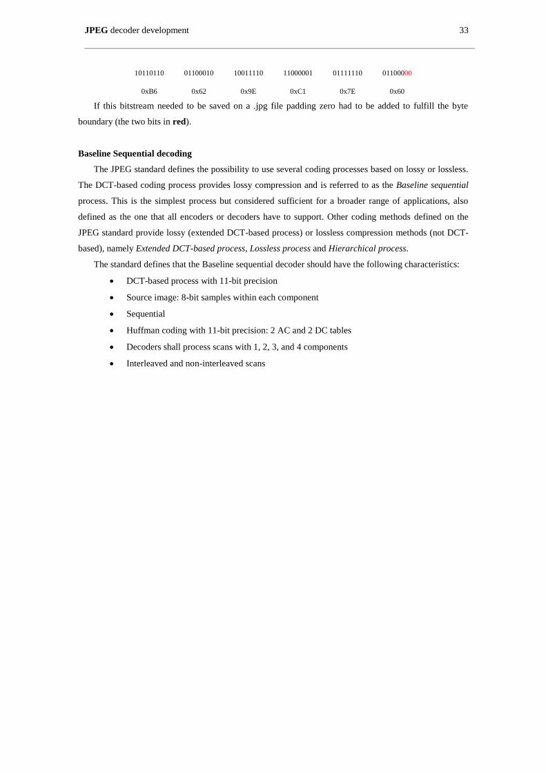
JPEG decoder development 33
10110110 01100010 10011110 11000001 01111110 01100000
0xB6 0x62 0x9E 0xC1 0x7E 0x60
If this bitstream needed to be saved on a .jpg file padding zero had to be added to fulfill the byte
boundary (the two bits in red).
Baseline Sequential decoding
The JPEG standard defines the possibility to use several coding processes based on lossy or lossless.
The DCT-based coding process provides lossy compression and is referred to as the Baseline sequential
process. This is the simplest process but considered sufficient for a broader range of applications, also
defined as the one that all encoders or decoders have to support. Other coding methods defined on the
JPEG standard provide lossy (extended DCT-based process) or lossless compression methods (not DCT-
based), namely Extended DCT-based process, Lossless process and Hierarchical process.
The standard defines that the Baseline sequential decoder should have the following characteristics:
DCT-based process with 11-bit precision
Source image: 8-bit samples within each component
Sequential
Huffman coding with 11-bit precision: 2 AC and 2 DC tables
Decoders shall process scans with 1, 2, 3, and 4 components
Interleaved and non-interleaved scans
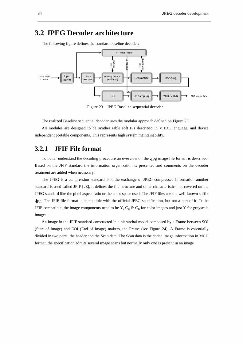
34 JPEG decoder development
3.2 JPEG Decoder architecture
The following figure defines the standard baseline decoder:
Input Buffer
Check0xFF 0x00
Entropy Decoder (Huffman)
Dequantize DeZigZag
IDCT Up Sampling YCbCr2RGB RGB Image Data
JFIF / JPEG stream
JFIF data reader
Quantizatio
n Tables
Hu
ffman
Ta
ble
s
Sampling
Figure 23 – JPEG Baseline sequential decoder
The realized Baseline sequential decoder uses the modular approach defined on Figure 23.
All modules are designed to be synthesizable soft IPs described in VHDL language, and device
independent portable components. This represents high system maintainability.
3.2.1 JFIF File format
To better understand the decoding procedure an overview on the .jpg image file format is described.
Based on the JFIF standard the information organization is presented and comments on the decoder
treatment are added when necessary.
The JPEG is a compression standard. For the exchange of JPEG compressed information another
standard is used called JFIF [28], it defines the file structure and other characteristics not covered on the
JPEG standard like the pixel aspect ratio or the color space used. The JFIF files use the well-known suffix
.jpg. The JFIF file format is compatible with the official JPEG specification, but not a part of it. To be
JFIF compatible, the image components need to be Y, CB & CR for color images and just Y for grayscale
images.
An image in the JFIF standard constructed in a hierarchal model composed by a Frame between SOI
(Start of Image) and EOI (End of Image) makers, the Frame (see Figure 24). A Frame is essentially
divided in two parts: the header and the Scan data. The Scan data is the coded image information in MCU
format, the specification admits several image scans but normally only one is present in an image.
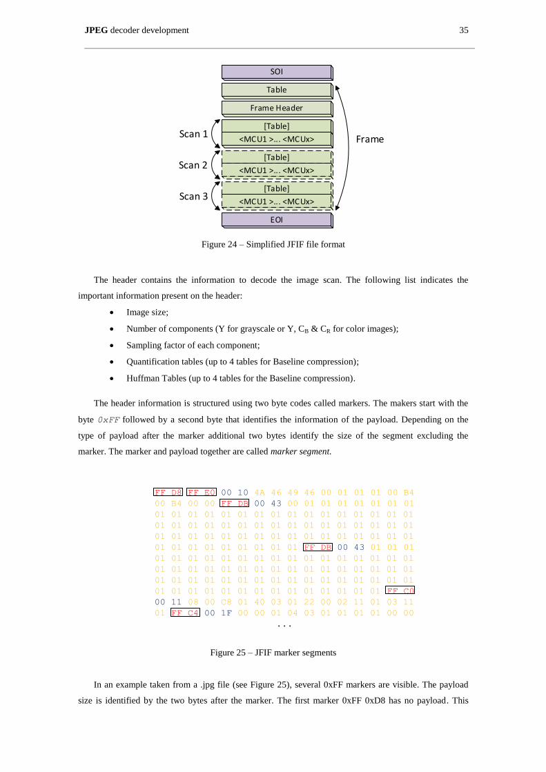
JPEG decoder development 35
SOI
Table
Frame Header
[Table]
<MCU1 >... <MCUx>
[Table]
<MCU1 >... <MCUx>
EOI
[Table]
<MCU1 >... <MCUx>
Scan 1
Scan 2
Scan 3
Frame
Figure 24 – Simplified JFIF file format
The header contains the information to decode the image scan. The following list indicates the
important information present on the header:
Image size;
Number of components (Y for grayscale or Y, CB & CR for color images);
Sampling factor of each component;
Quantification tables (up to 4 tables for Baseline compression);
Huffman Tables (up to 4 tables for the Baseline compression).
The header information is structured using two byte codes called markers. The makers start with the
byte 0xFF followed by a second byte that identifies the information of the payload. Depending on the
type of payload after the marker additional two bytes identify the size of the segment excluding the
marker. The marker and payload together are called marker segment.
FF D8 FF E0 00 10 4A 46 49 46 00 01 01 01 00 B4
00 B4 00 00 FF DB 00 43 00 01 01 01 01 01 01 01
01 01 01 01 01 01 01 01 01 01 01 01 01 01 01 01
01 01 01 01 01 01 01 01 01 01 01 01 01 01 01 01
01 01 01 01 01 01 01 01 01 01 01 01 01 01 01 01
01 01 01 01 01 01 01 01 01 FF DB 00 43 01 01 01
01 01 01 01 01 01 01 01 01 01 01 01 01 01 01 01
01 01 01 01 01 01 01 01 01 01 01 01 01 01 01 01
01 01 01 01 01 01 01 01 01 01 01 01 01 01 01 01
01 01 01 01 01 01 01 01 01 01 01 01 01 01 FF C0
00 11 08 00 C8 01 40 03 01 22 00 02 11 01 03 11
01 FF C4 00 1F 00 00 01 04 03 01 01 01 01 00 00
...
Figure 25 – JFIF marker segments
In an example taken from a .jpg file (see Figure 25), several 0xFF markers are visible. The payload
size is identified by the two bytes after the marker. The first marker 0xFF 0xD8 has no payload. This
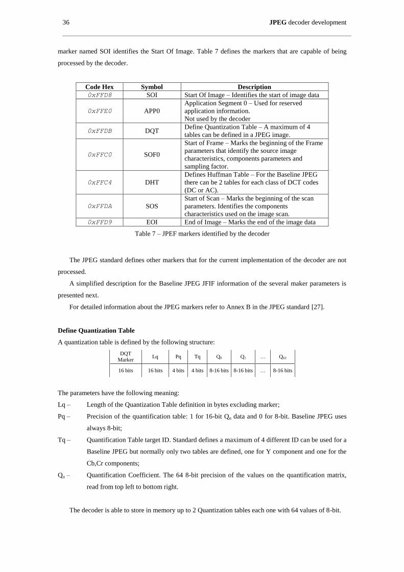
36 JPEG decoder development
marker named SOI identifies the Start Of Image. Table 7 defines the markers that are capable of being
processed by the decoder.
Code Hex Symbol Description
0xFFD8 SOI Start Of Image – Identifies the start of image data
0xFFE0 APP0
Application Segment 0 – Used for reserved
application information.
Not used by the decoder
0xFFDB DQT Define Quantization Table – A maximum of 4
tables can be defined in a JPEG image.
0xFFC0 SOF0
Start of Frame – Marks the beginning of the Frame
parameters that identify the source image
characteristics, components parameters and
sampling factor.
0xFFC4 DHT
Defines Huffman Table – For the Baseline JPEG
there can be 2 tables for each class of DCT codes
(DC or AC).
0xFFDA SOS
Start of Scan – Marks the beginning of the scan
parameters. Identifies the components
characteristics used on the image scan.
0xFFD9 EOI End of Image – Marks the end of the image data
Table 7 – JPEF markers identified by the decoder
The JPEG standard defines other markers that for the current implementation of the decoder are not
processed.
A simplified description for the Baseline JPEG JFIF information of the several maker parameters is
presented next.
For detailed information about the JPEG markers refer to Annex B in the JPEG standard [27].
Define Quantization Table
A quantization table is defined by the following structure:
DQT
Marker Lq Pq Tq Q0 Q1 … Q63
16 bits 16 bits 4 bits 4 bits 8-16 bits 8-16 bits … 8-16 bits
The parameters have the following meaning:
Lq – Length of the Quantization Table definition in bytes excluding marker;
Pq – Precision of the quantification table: 1 for 16-bit Qn data and 0 for 8-bit. Baseline JPEG uses
always 8-bit;
Tq – Quantification Table target ID. Standard defines a maximum of 4 different ID can be used for a
Baseline JPEG but normally only two tables are defined, one for Y component and one for the
Cb,Cr components;
Qn – Quantification Coefficient. The 64 8-bit precision of the values on the quantification matrix,
read from top left to bottom right.
The decoder is able to store in memory up to 2 Quantization tables each one with 64 values of 8-bit.
JPEG decoder development 37
Define Huffman Table
A Huffman table is defined by the following structure:
DHT
Marker Lh Tc Th L1 L2 … L16
[L1
Symbols] …
[L16
Symbols]
16 bits 16 bits 4 bits 4 bits 8 bits 8 bits … 8 bits 8 bits per symbol
… 8 bits per symbol
The parameters have the following meaning:
Lh – Length of the Huffman Table definition in bytes excluding marker;
Tc – Table Class. Defines the DC or AC class of the Huffman symbols being defined. Value 0 for
DC and 1 for AC;
Th – Huffman Table target ID. A maximum of 2 different ID can be used for a Baseline JPEG;
Li – Number of Huffman codes of length i. The maximum code length is 16. If no code exists for a
length i, a 0 value will be used;
[Li symbols] – Depending on the number of Huffman codes for each length, the symbols are defined
starting on length 1 until 16. The symbol will be defined by [SIZE] for a DC table or [RUN
SIZE] for AC class tables. An example is given above.
DHT
Marker Lh Tc Th L1 L2 L3 L4 L5-16 [L2 symbols] [L4 symbols]
0xFFC4 0x17 0x10 0x00 0x01 0x00 0x03 0x00 0x23 0x00 0x12 0x04
The decoder from the information on the number of symbols for each length must be able to generate
the Huffman codes. The symbols need also to be stored in distributed memory for the decoding process.
Start Of Frame0
The SOF0 is defined by the following structure:
SOF0 Marker
Lf P Y X Nf [Component1 parameters]
[Component2 parameters]
[Component3 parameters]
16 bits 16 bits 8 bits 16 bits 16 bits 8 bits [24 bits] [24 bits] [24 bits]
The component parameters will be:
Ci Hi Vi Tqi
8 bits 8 bits 4 bits 8 bits
The parameters have the following meaning:
Lf – Length of the Frame definition in bytes excluding marker;
P – Precision. Defines the sample precision of the components in the frame. Always 8-bit precision
for Baseline JPEG;
Y – Number of lines in the image. The JPEG standard defines that the Y parameter for the frame
can be 0 and be defined on the DNL marker. The decoder expects a value different from zero
on this parameter;
38 JPEG decoder development
X – Number of columns in the image. The JPEG standard defines that the X parameter for the
frame can be 0 and be defined on the DNL marker. The decoder expects a value different from
zero on this parameter;
Nf – Number of components in frame. It will indicate to the decoder the number of components
present in the file. The decoder is prepared to read the parameters for a maximum of 3
components for color images, Y, CB & CR;
Ci – Component Identification. The identification of the components will be used to identify the
components on the scan header. A normal identification will be, 0x01 for Y, 0x02 for CB and
0x03 for CR;
Hi – Horizontal Sampling factor. Defines the number of component horizontal blocks there are in a
MCU. A value 0x2 will indicate that there are 2 blocks of this component in the horizontal
dimension of the MCU;
Vi – Vertical Sampling factor. Defines the number of component vertical blocks there are in a
MCU. A value 0x2 will indicate that there are 2 blocks of this component in the vertical
dimension of the MCU.
The decoder is able to define the sampling factor by the information of each component Hi and Vi.
The following table defines the values for the standard sampling factors:
Component Sampling Factor
ID
MCU size
HxV pixels Y Cb Cr
Hi Vi Hi Vi Hi Vi
0x11 0x11 0x11 4:4:4 8x8
0x22 0x11 0x11 4:2:0 16x16
0x21 0x11 0x11 4:2:2 16x8
0x11 -- -- Gray 8x8
Table 8 – Frame Sampling Factor identification
Tqi – Quantization Table Identification. Defines the quantification ID to use for the component.
Start Of Scan
The SOS is defined by the following structure:
SOS
Marker Ls Ns
[Component1
parameters]
[Component2
parameters]
[Component3
parameters] Ss Se Ah Al
16 bits 16 bits 8 bits [16bits] [16 bits] [16 bits] 8 bits 8 bits 4 bits 4 bits
The component parameters will be:
Csi Tdi Tai
8 bits 4 bits 4 bits
The parameters have the following meaning:
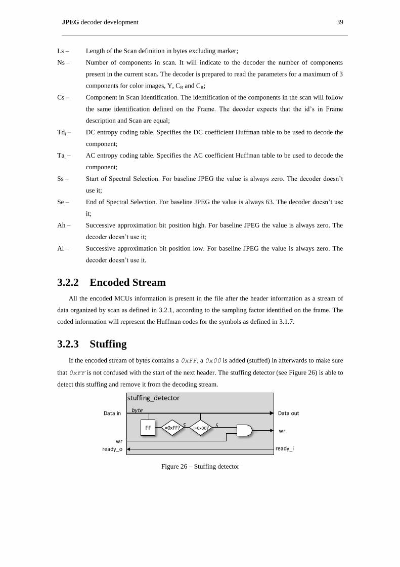
JPEG decoder development 39
Ls – Length of the Scan definition in bytes excluding marker;
Ns – Number of components in scan. It will indicate to the decoder the number of components
present in the current scan. The decoder is prepared to read the parameters for a maximum of 3
components for color images, Y, CB and CR;
Cs – Component in Scan Identification. The identification of the components in the scan will follow
the same identification defined on the Frame. The decoder expects that the id’s in Frame
description and Scan are equal;
Tdi – DC entropy coding table. Specifies the DC coefficient Huffman table to be used to decode the
component;
Tai – AC entropy coding table. Specifies the AC coefficient Huffman table to be used to decode the
component;
Ss – Start of Spectral Selection. For baseline JPEG the value is always zero. The decoder doesn’t
use it;
Se – End of Spectral Selection. For baseline JPEG the value is always 63. The decoder doesn’t use
it;
Ah – Successive approximation bit position high. For baseline JPEG the value is always zero. The
decoder doesn’t use it;
Al – Successive approximation bit position low. For baseline JPEG the value is always zero. The
decoder doesn’t use it.
3.2.2 Encoded Stream
All the encoded MCUs information is present in the file after the header information as a stream of
data organized by scan as defined in 3.2.1, according to the sampling factor identified on the frame. The
coded information will represent the Huffman codes for the symbols as defined in 3.1.7.
3.2.3 Stuffing
If the encoded stream of bytes contains a 0xFF, a 0x00 is added (stuffed) in afterwards to make sure
that 0xFF is not confused with the start of the next header. The stuffing detector (see Figure 26) is able to
detect this stuffing and remove it from the decoding stream.
stuffing_detector
FF
Data in
ready_o
Data out
ready_i
byte
S=0xFF? !=0x00?S
wr
wr
Figure 26 – Stuffing detector

40 JPEG decoder development
3.3 Developed Static JPEG Decoder
In this thesis the first approach to the JPEG decoder was a static implementation of the decoder on
the fabric. This enabled the development of the modules used to implement the JPEG using dynamic
reconfiguration and also to have a comparable approach.
Several VHDL description files were used to implement the different modules of the decoder. The
following figure gives the overview of the modules base description files.
JPEG Decoder (top)
Input Buffer
Check0xFF 0x00
Entropy Decoder (Huffman)
DequantizeDPCM
RLE Expand DeZigZag
IDCT Up Sampling YCbCr2RGB RGB Image Data
JFIF / JPEG stream
JFIF data reader
Qu
an
tizatio
n
Tables
Hu
ffman
Ta
ble
s
Sampling
huffman_decoder
idct_core mcu_upsampling
sr_input
mcu_YCbCr2RGB
zrl_decoder
Image data
Decoding Statusstart of picture, end of image
x size, y size, sampling
Figure 27 – JPEG Baseline module description files
3.3.1 JPEG Decoder top entity
The JPEG Decoder top entity represents the several logic data modules. It defines the interface
between this modules and the I/O interface of the decoder with the system.
The JPEG interface is composed by the input interface where the data JFIF stream in 32-bit word
format is read and the output interface were the decoded data and status information is given.
Figure 28 – jpeg_decoder top entity
The detailed signals are described on Table 9. It also defines each signal group, width and direction.
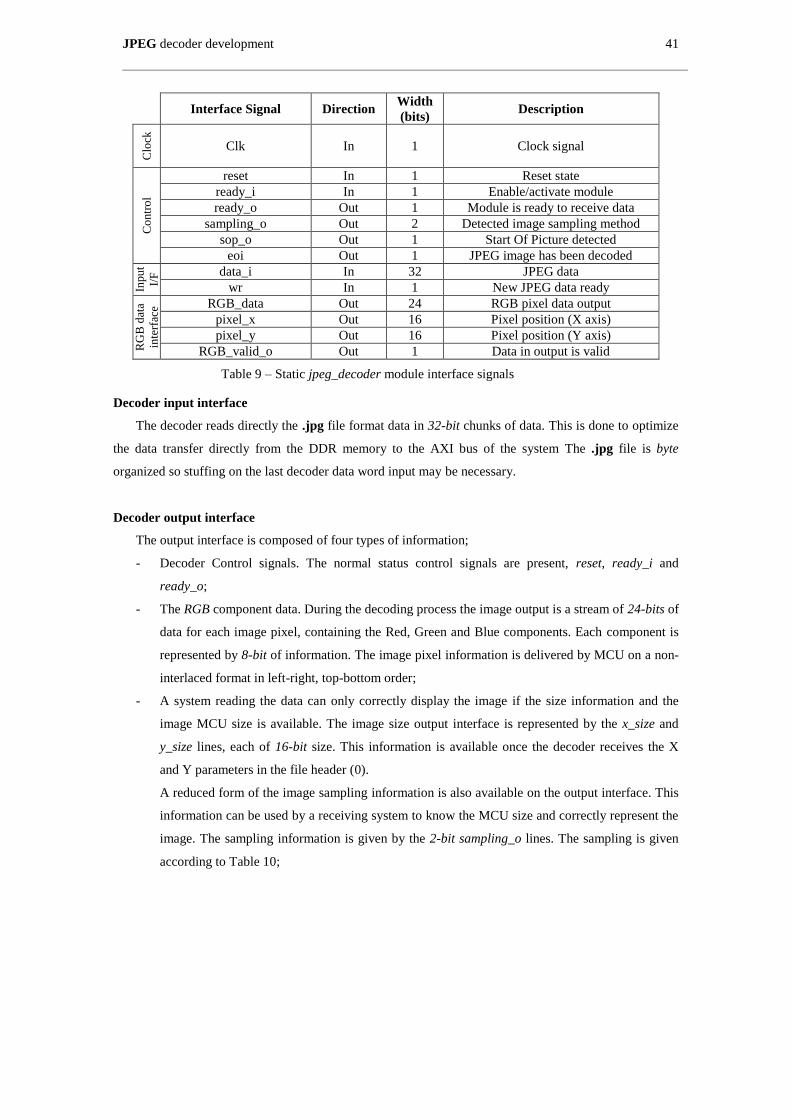
JPEG decoder development 41
Interface Signal Direction
Width
(bits) Description
Clo
ck
Clk In 1 Clock signal C
on
tro
l
reset In 1 Reset state
ready_i In 1 Enable/activate module
ready_o Out 1 Module is ready to receive data
sampling_o Out 2 Detected image sampling method
sop_o Out 1 Start Of Picture detected
eoi Out 1 JPEG image has been decoded
Inpu
t
I/F
data_i In 32 JPEG data
wr In 1 New JPEG data ready
RG
B d
ata
inte
rfac
e RGB_data Out 24 RGB pixel data output
pixel_x Out 16 Pixel position (X axis)
pixel_y Out 16 Pixel position (Y axis)
RGB_valid_o Out 1 Data in output is valid
Table 9 – Static jpeg_decoder module interface signals
Decoder input interface
The decoder reads directly the .jpg file format data in 32-bit chunks of data. This is done to optimize
the data transfer directly from the DDR memory to the AXI bus of the system The .jpg file is byte
organized so stuffing on the last decoder data word input may be necessary.
Decoder output interface
The output interface is composed of four types of information;
- Decoder Control signals. The normal status control signals are present, reset, ready_i and
ready_o;
- The RGB component data. During the decoding process the image output is a stream of 24-bits of
data for each image pixel, containing the Red, Green and Blue components. Each component is
represented by 8-bit of information. The image pixel information is delivered by MCU on a non-
interlaced format in left-right, top-bottom order;
- A system reading the data can only correctly display the image if the size information and the
image MCU size is available. The image size output interface is represented by the x_size and
y_size lines, each of 16-bit size. This information is available once the decoder receives the X
and Y parameters in the file header (0).
A reduced form of the image sampling information is also available on the output interface. This
information can be used by a receiving system to know the MCU size and correctly represent the
image. The sampling information is given by the 2-bit sampling_o lines. The sampling is given
according to Table 10;
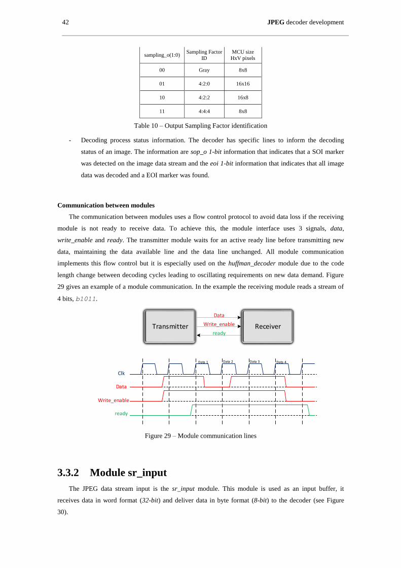
42 JPEG decoder development
sampling_o(1:0) Sampling Factor
ID
MCU size
HxV pixels
00 Gray 8x8
01 4:2:0 16x16
10 4:2:2 16x8
11 4:4:4 8x8
Table 10 – Output Sampling Factor identification
- Decoding process status information. The decoder has specific lines to inform the decoding
status of an image. The information are sop_o 1-bit information that indicates that a SOI marker
was detected on the image data stream and the eoi 1-bit information that indicates that all image
data was decoded and a EOI marker was found.
Communication between modules
The communication between modules uses a flow control protocol to avoid data loss if the receiving
module is not ready to receive data. To achieve this, the module interface uses 3 signals, data,
write_enable and ready. The transmitter module waits for an active ready line before transmitting new
data, maintaining the data available line and the data line unchanged. All module communication
implements this flow control but it is especially used on the huffman_decoder module due to the code
length change between decoding cycles leading to oscillating requirements on new data demand. Figure
29 gives an example of a module communication. In the example the receiving module reads a stream of
4 bits, b1011.
ReceiverTransmitter
Data
Write_enable
ready
Clk
Data
Write_enable
ready
Data 2 Data 3 Data 4Data 1
Figure 29 – Module communication lines
3.3.2 Module sr_input
The JPEG data stream input is the sr_input module. This module is used as an input buffer, it
receives data in word format (32-bit) and deliver data in byte format (8-bit) to the decoder (see Figure
30).
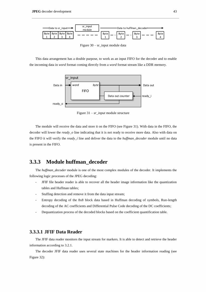
JPEG decoder development 43
Byte 1
Byte 2
Byte 3
Byte 4
Byte 1
Byte 2
Byte 3
Byte 4
Data to sr_input Data to huffman_decodersr_inputmodule
Figure 30 – sr_input module data
This data arrangement has a double purpose, to work as an input FIFO for the decoder and to enable
the incoming data in word format coming directly from a word format stream like a DDR memory.
sr_input
FIFOData out counter
Data in
ready_o
Data out
ready_i
word byte
Figure 31 – sr_input module structure
The module will receive the data and store it on the FIFO (see Figure 31). With data in the FIFO, the
decoder will lower the ready_o line indicating that it is not ready to receive more data. Also with data on
the FIFO it will verify the ready_i line and deliver the data to the huffman_decoder module until no data
is present in the FIFO.
3.3.3 Module huffman_decoder
The huffman_decoder module is one of the most complex modules of the decoder. It implements the
following logic processes of the JPEG decoding:
- JFIF file header reader is able to recover all the header image information like the quantization
tables and Huffman tables;
- Stuffing detection and remove it from the data input stream;
- Entropy decoding of the 8x8 block data based in Huffman decoding of symbols, Run-length
decoding of the AC coefficients and Differential Pulse Code decoding of the DC coefficients;
- Dequantization process of the decoded blocks based on the coefficient quantification table.
3.3.3.1 JFIF Data Reader
The JFIF data reader monitors the input stream for markers. It is able to detect and retrieve the header
information according to 3.2.1.
The decoder JFIF data reader uses several state machines for the header information reading (see
Figure 32):
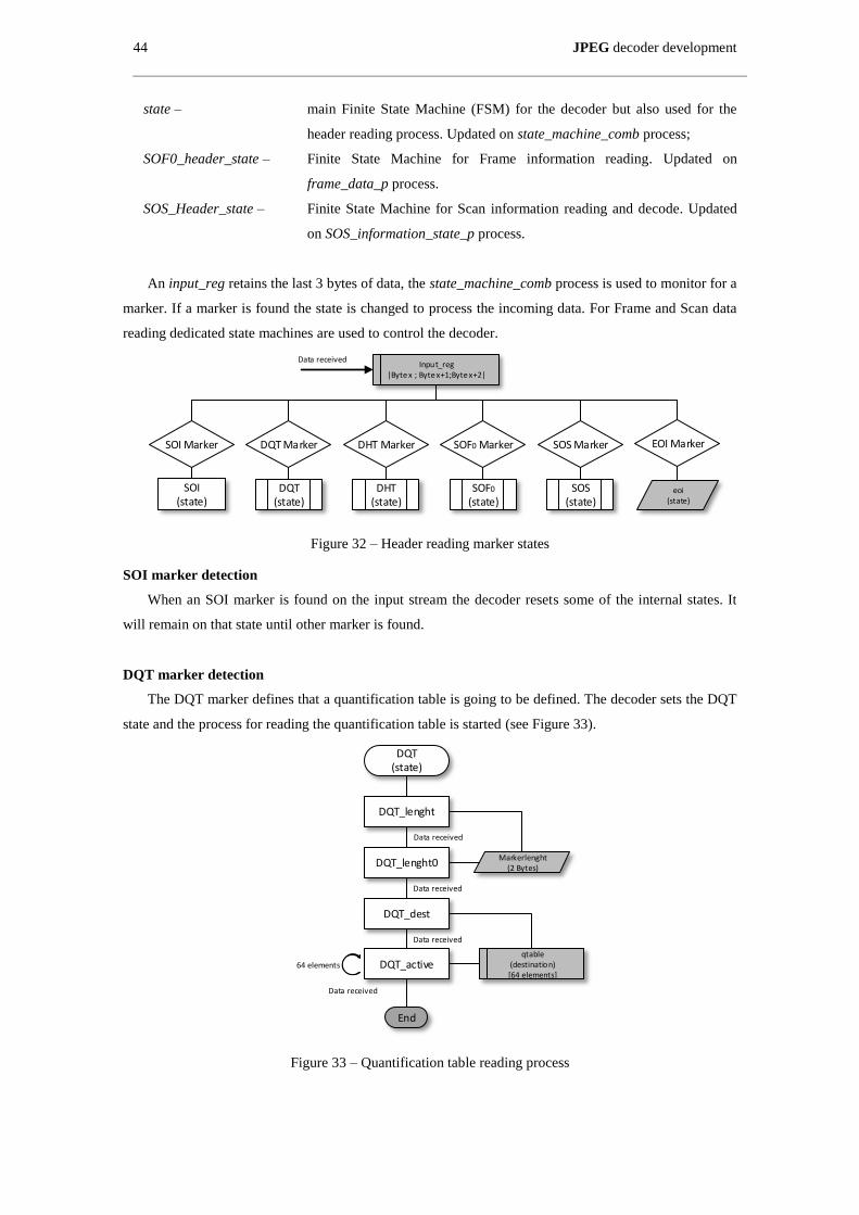
44 JPEG decoder development
state – main Finite State Machine (FSM) for the decoder but also used for the
header reading process. Updated on state_machine_comb process;
SOF0_header_state – Finite State Machine for Frame information reading. Updated on
frame_data_p process.
SOS_Header_state – Finite State Machine for Scan information reading and decode. Updated
on SOS_information_state_p process.
An input_reg retains the last 3 bytes of data, the state_machine_comb process is used to monitor for a
marker. If a marker is found the state is changed to process the incoming data. For Frame and Scan data
reading dedicated state machines are used to control the decoder.
DQT Marker
DQT(state)
DHT Marker
DHT(state)
Input_reg|Byte x ; Byte x+1;Byte x+2|
Data received
SOF0 Marker
SOF0
(state)
SOS Marker
SOS(state)
SOI Marker
SOI(state)
EOI Marker
eoi(state)
Figure 32 – Header reading marker states
SOI marker detection
When an SOI marker is found on the input stream the decoder resets some of the internal states. It
will remain on that state until other marker is found.
DQT marker detection
The DQT marker defines that a quantification table is going to be defined. The decoder sets the DQT
state and the process for reading the quantification table is started (see Figure 33).
DQT_lenght
DQT_lenght0
DQT_dest
DQT_active
Data received
Data received
Markerlenght(2 Bytes)
64 elements
Data received
Data received
qtable(destination)[64 elements]
DQT(state)
End
Figure 33 – Quantification table reading process
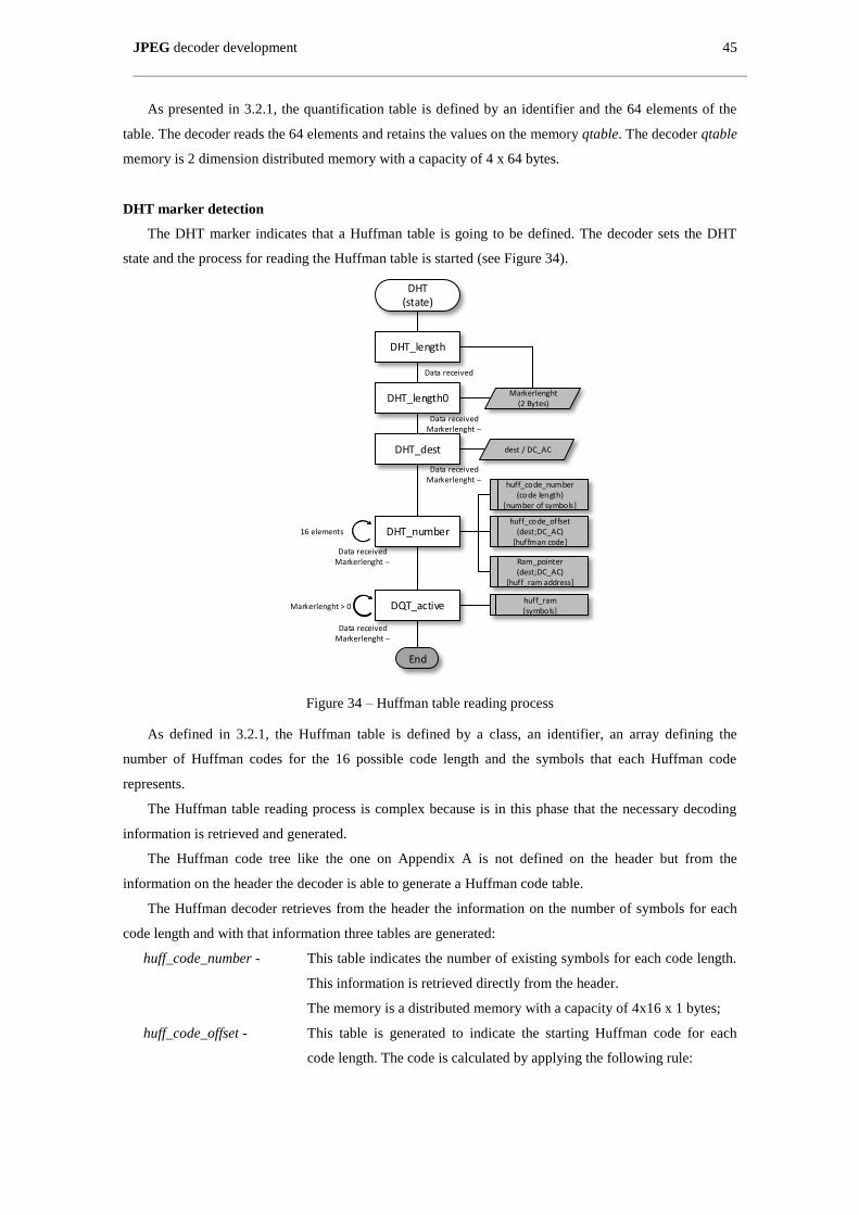
JPEG decoder development 45
As presented in 3.2.1, the quantification table is defined by an identifier and the 64 elements of the
table. The decoder reads the 64 elements and retains the values on the memory qtable. The decoder qtable
memory is 2 dimension distributed memory with a capacity of 4 x 64 bytes.
DHT marker detection
The DHT marker indicates that a Huffman table is going to be defined. The decoder sets the DHT
state and the process for reading the Huffman table is started (see Figure 34).
DHT_length
DHT_length0
DHT_dest
DQT_active
Data received
Data receivedMarkerlenght --
Markerlenght(2 Bytes)
Markerlenght > 0
Data receivedMarkerlenght --
Data receivedMarkerlenght --
huff_ram[symbols]
DHT(state)
End
DHT_number
dest / DC_AC
Data receivedMarkerlenght --
16 elements
huff_code_number(code length)
[number of symbols]
Ram_pointer (dest;DC_AC)
[huff_ram address]
huff_code_offset(dest;DC_AC)
[huffman code]
Figure 34 – Huffman table reading process
As defined in 3.2.1, the Huffman table is defined by a class, an identifier, an array defining the
number of Huffman codes for the 16 possible code length and the symbols that each Huffman code
represents.
The Huffman table reading process is complex because is in this phase that the necessary decoding
information is retrieved and generated.
The Huffman code tree like the one on Appendix A is not defined on the header but from the
information on the header the decoder is able to generate a Huffman code table.
The Huffman decoder retrieves from the header the information on the number of symbols for each
code length and with that information three tables are generated:
huff_code_number - This table indicates the number of existing symbols for each code length.
This information is retrieved directly from the header.
The memory is a distributed memory with a capacity of 4x16 x 1 bytes;
huff_code_offset - This table is generated to indicate the starting Huffman code for each
code length. The code is calculated by applying the following rule:
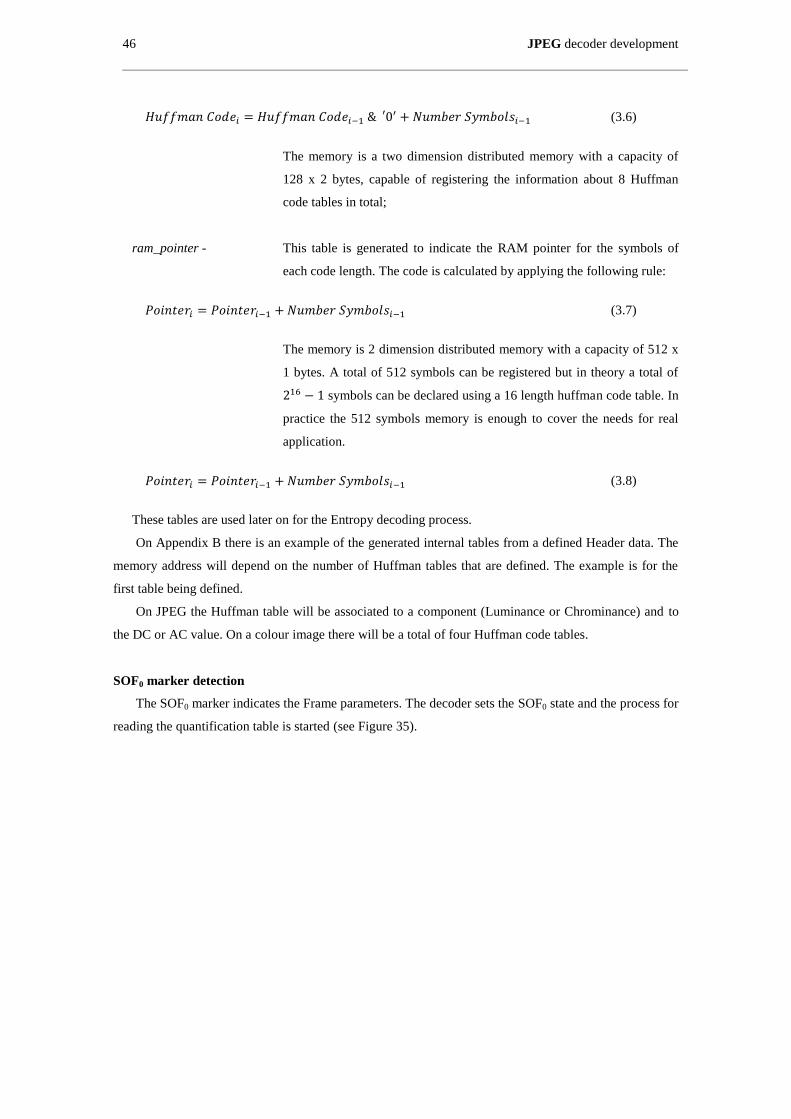
46 JPEG decoder development
(3.6)
The memory is a two dimension distributed memory with a capacity of
128 x 2 bytes, capable of registering the information about 8 Huffman
code tables in total;
ram_pointer - This table is generated to indicate the RAM pointer for the symbols of
each code length. The code is calculated by applying the following rule:
(3.7)
The memory is 2 dimension distributed memory with a capacity of 512 x
1 bytes. A total of 512 symbols can be registered but in theory a total of
symbols can be declared using a 16 length huffman code table. In
practice the 512 symbols memory is enough to cover the needs for real
application.
(3.8)
These tables are used later on for the Entropy decoding process.
On Appendix B there is an example of the generated internal tables from a defined Header data. The
memory address will depend on the number of Huffman tables that are defined. The example is for the
first table being defined.
On JPEG the Huffman table will be associated to a component (Luminance or Chrominance) and to
the DC or AC value. On a colour image there will be a total of four Huffman code tables.
SOF0 marker detection
The SOF0 marker indicates the Frame parameters. The decoder sets the SOF0 state and the process for
reading the quantification table is started (see Figure 35).
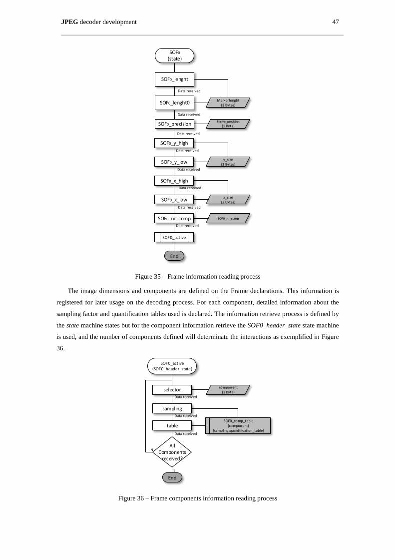
JPEG decoder development 47
SOF0_lenght
SOF0_lenght0
SOF0_precision
Data received
Data received
Markerlenght(2 Bytes)
SOF0
(state)
SOF0_y_high
Data received
SOF0_y_low
Data received
SOF0_x_high
SOF0_x_low
SOF0_nr_comp
SOF0_act ive
End
Data received
Data received
Data received
Data received
Frame_precision
(1 Byte)
y_size(2 Bytes)
x_size(2 Bytes)
SOF0_nr_comp
Figure 35 – Frame information reading process
The image dimensions and components are defined on the Frame declarations. This information is
registered for later usage on the decoding process. For each component, detailed information about the
sampling factor and quantification tables used is declared. The information retrieve process is defined by
the state machine states but for the component information retrieve the SOF0_header_state state machine
is used, and the number of components defined will determinate the interactions as exemplified in Figure
36.
SOF0_act ive(SOF0_header_state)
SOF0_comp_table(component)
[sampling;quantification_table]
All Components
received?
selector
sampling
End
Data received
Data received
table
component(1 Byte)
Data received
S
N
Figure 36 – Frame components information reading process
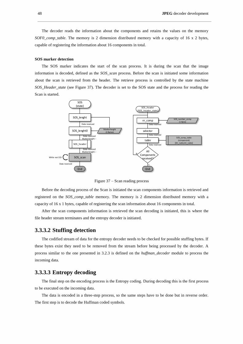
48 JPEG decoder development
The decoder reads the information about the components and retains the values on the memory
SOF0_comp_table. The memory is 2 dimension distributed memory with a capacity of 16 x 2 bytes,
capable of registering the information about 16 components in total.
SOS marker detection
The SOS marker indicates the start of the scan process. It is during the scan that the image
information is decoded, defined as the SOS_scan process. Before the scan is initiated some information
about the scan is retrieved from the header. The retrieve process is controlled by the state machine
SOS_Header_state (see Figure 37). The decoder is set to the SOS state and the process for reading the
Scan is started.
SOS_lenght
SOS_lenght0
SOS_header
Data received
Data receivedMarkerlenght --
Markerlenght(2 Bytes)
Data receivedMarkerlenght --
SOS(state)
End
SOS_scan
Data received
While not EOI
SOS_header(SOS_header_state)
SOS_comp_table(component)
[DC_table;AC_table]
All Components
received?
nr_comp
selector
End
Data received
Data received
table
SOS_number_comp(1 Byte)
Data received
S
N
Figure 37 – Scan reading process
Before the decoding process of the Scan is initiated the scan components information is retrieved and
registered on the SOS_comp_table memory. The memory is 2 dimension distributed memory with a
capacity of 16 x 1 bytes, capable of registering the scan information about 16 components in total.
After the scan components information is retrieved the scan decoding is initiated, this is where the
file header stream terminates and the entropy decoder is initiated.
3.3.3.2 Stuffing detection
The codified stream of data for the entropy decoder needs to be checked for possible stuffing bytes. If
these bytes exist they need to be removed from the stream before being processed by the decoder. A
process similar to the one presented in 3.2.3 is defined on the huffman_decoder module to process the
incoming data.
3.3.3.3 Entropy decoding
The final step on the encoding process is the Entropy coding. During decoding this is the first process
to be executed on the incoming data.
The data is encoded in a three-step process, so the same steps have to be done but in reverse order.
The first step is to decode the Huffman coded symbols.
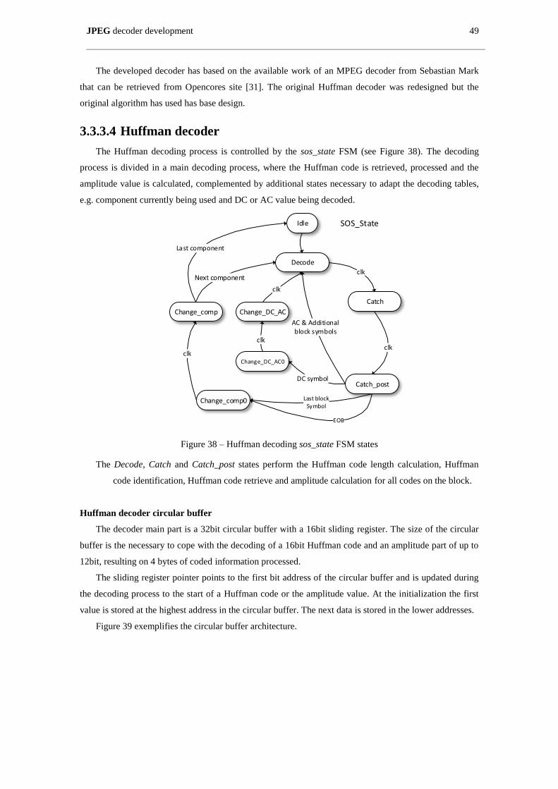
JPEG decoder development 49
The developed decoder has based on the available work of an MPEG decoder from Sebastian Mark
that can be retrieved from Opencores site [31]. The original Huffman decoder was redesigned but the
original algorithm has used has base design.
3.3.3.4 Huffman decoder
The Huffman decoding process is controlled by the sos_state FSM (see Figure 38). The decoding
process is divided in a main decoding process, where the Huffman code is retrieved, processed and the
amplitude value is calculated, complemented by additional states necessary to adapt the decoding tables,
e.g. component currently being used and DC or AC value being decoded.
Decode
Catch
Idle
Catch_post
Change_comp0
Change_comp
Change_DC_AC0
Change_DC_AC
Next component
clk
SOS_State
Figure 38 – Huffman decoding sos_state FSM states
The Decode, Catch and Catch_post states perform the Huffman code length calculation, Huffman
code identification, Huffman code retrieve and amplitude calculation for all codes on the block.
Huffman decoder circular buffer
The decoder main part is a 32bit circular buffer with a 16bit sliding register. The size of the circular
buffer is the necessary to cope with the decoding of a 16bit Huffman code and an amplitude part of up to
12bit, resulting on 4 bytes of coded information processed.
The sliding register pointer points to the first bit address of the circular buffer and is updated during
the decoding process to the start of a Huffman code or the amplitude value. At the initialization the first
value is stored at the highest address in the circular buffer. The next data is stored in the lower addresses.
Figure 39 exemplifies the circular buffer architecture.
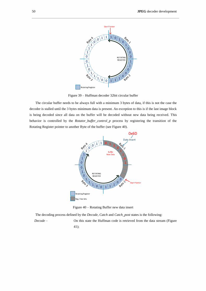
50 JPEG decoder development
10
011 0
00
10
1
10
1
0
1
0
1
1 1
1
1
1
0
0
0
0
0 0 1
1 1
Start Pointer
ROTATINGREGISTER
Rotating Register
Figure 39 – Huffman decoder 32bit circular buffer
The circular buffer needs to be always full with a minimum 3 bytes of data, if this is not the case the
decoder is stalled until the 3 bytes minimum data is present. An exception to this is if the last image block
is being decoded since all data on the buffer will be decoded without new data being received. This
behavior is controlled by the Rotator_buffer_control_p process by registering the transition of the
Rotating Register pointer to another Byte of the buffer (see Figure 40).
1
011 1
00
10
1
10
1
0
1
0
1
1 1
1
1
0
0
1
0 0 1
1 0
Start Pointer
ROTATINGREGISTER
Reg. Free bits
Rotating Register
BufferNew Data
0x6D
Figure 40 – Rotating Buffer new data insert
The decoding process defined by the Decode, Catch and Catch_post states is the following:
Decode – On this state the Huffman code is retrieved from the data stream (Figure
41);
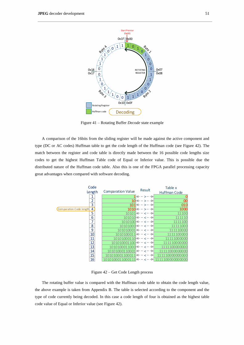
JPEG decoder development 51
10
011 0
00
10
1
10
1
0
1
0
1
1 1
1
11
0
0
0
0
0 0 1
1 1
Start Pointer(0x00)
ROTATINGREGISTER
DecodingHuffman code
Rotating Register
0x00
0x070x08
0x0F0x10
0x170x18
0x1F
Figure 41 – Rotating Buffer Decode state example
A comparison of the 16bits from the sliding register will be made against the active component and
type (DC or AC codes) Huffman table to get the code length of the Huffman code (see Figure 42). The
match between the register and code table is directly made between the 16 possible code lengths size
codes to get the highest Huffman Table code of Equal or Inferior value. This is possible due the
distributed nature of the Huffman code table. Also this is one of the FPGA parallel processing capacity
great advantages when compared with software decoding.
000
Table xHuffman Code
010
11100111110
111110011111000
1111100001111100000
11111000000111110000000
111110000000011111000000000
1111100000000001111100000000000
1000
110
Comparation Value
101
10101101010
101010010101000
1010100011010100011
10101000110101010001100
101010001100010101000110001
1010100011000111010100011000111
1010
12
Code Length
3
56789
10111213141516
4
>>
>>
<Comparation Code length
<<<<<<<<<<<
Result
Figure 42 – Get Code Length process
The rotating buffer value is compared with the Huffman code table to obtain the code length value,
the above example is taken from Appendix B. The table is selected according to the component and the
type of code currently being decoded. In this case a code length of four is obtained as the highest table
code value of Equal or Inferior value (see Figure 42).
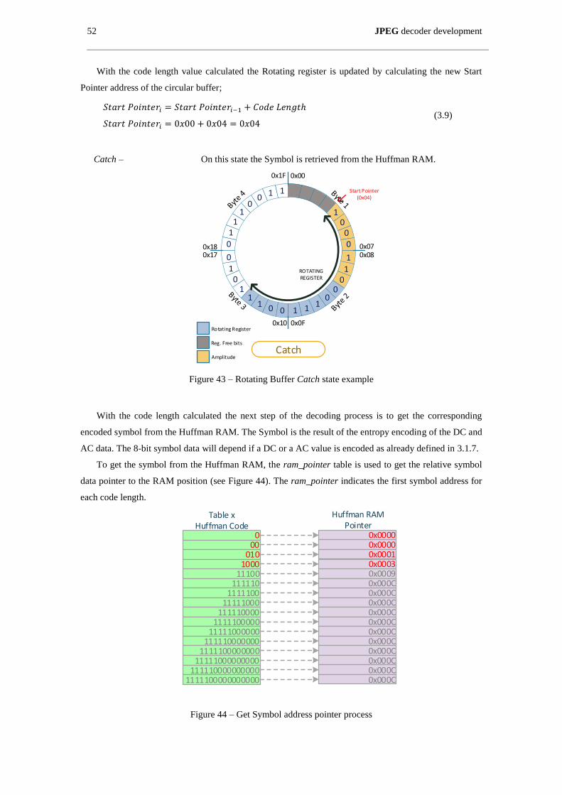
52 JPEG decoder development
With the code length value calculated the Rotating register is updated by calculating the new Start
Pointer address of the circular buffer;
(3.9)
Catch – On this state the Symbol is retrieved from the Huffman RAM.
10
011 0
00
10
1
10
1
0
11
1
1
11
0
0
0
0 0 1
1 Start Pointer(0x04)
ROTATINGREGISTER
CatchReg. Free bits
Amplitude
Rotating Register
0x00
0x070x08
0x0F0x10
0x170x18
0x1F
Figure 43 – Rotating Buffer Catch state example
With the code length calculated the next step of the decoding process is to get the corresponding
encoded symbol from the Huffman RAM. The Symbol is the result of the entropy encoding of the DC and
AC data. The 8-bit symbol data will depend if a DC or a AC value is encoded as already defined in 3.1.7.
To get the symbol from the Huffman RAM, the ram_pointer table is used to get the relative symbol
data pointer to the RAM position (see Figure 44). The ram_pointer indicates the first symbol address for
each code length.
000
Table xHuffman Code
010
11100111110
111110011111000
1111100001111100000
11111000000111110000000
111110000000011111000000000
1111100000000001111100000000000
1000
0x00000x0000
Huffman RAM Pointer
0x0001
0x00090x000C0x000C0x000C0x000C0x000C0x000C0x000C0x000C0x000C0x000C0x000C
0x0003
0x000C
Figure 44 – Get Symbol address pointer process
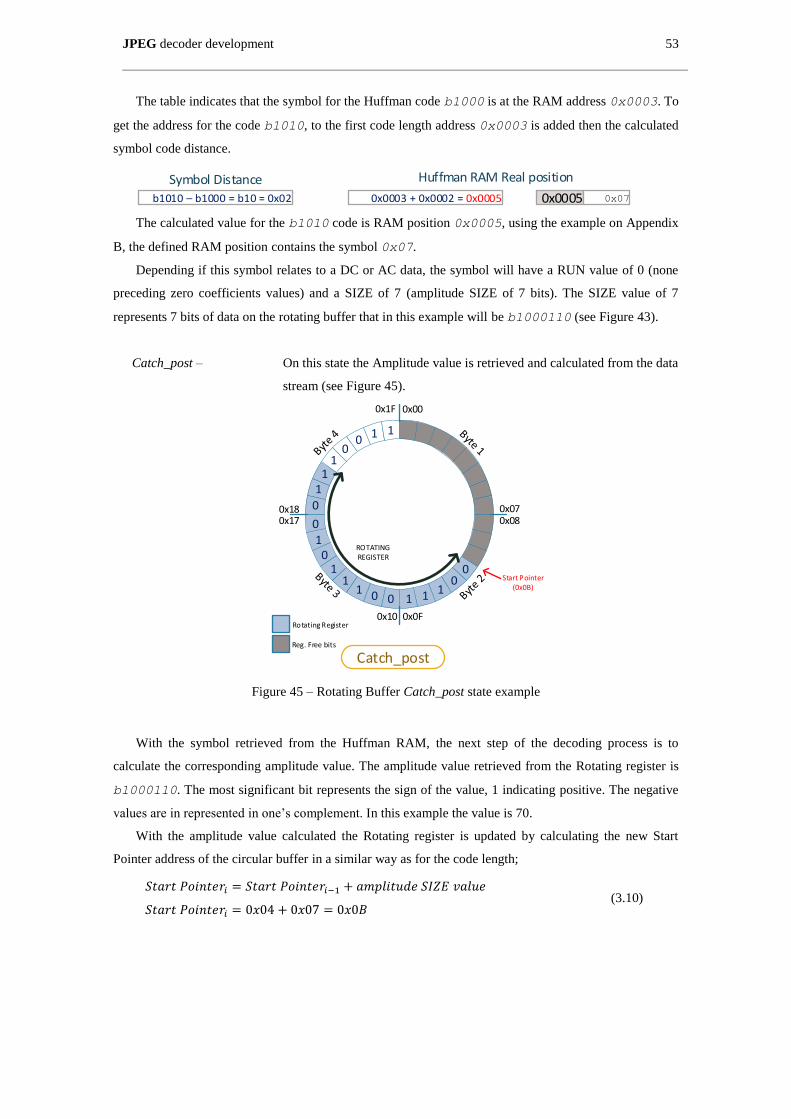
JPEG decoder development 53
The table indicates that the symbol for the Huffman code b1000 is at the RAM address 0x0003. To
get the address for the code b1010, to the first code length address 0x0003 is added then the calculated
symbol code distance.
b1010 – b1000 = b10 = 0x02
Symbol Distance Huffman RAM Real position
0x0003 + 0x0002 = 0x0005 0x0005 0x07
The calculated value for the b1010 code is RAM position 0x0005, using the example on Appendix
B, the defined RAM position contains the symbol 0x07.
Depending if this symbol relates to a DC or AC data, the symbol will have a RUN value of 0 (none
preceding zero coefficients values) and a SIZE of 7 (amplitude SIZE of 7 bits). The SIZE value of 7
represents 7 bits of data on the rotating buffer that in this example will be b1000110 (see Figure 43).
Catch_post – On this state the Amplitude value is retrieved and calculated from the data
stream (see Figure 45).
1
11
00
10
10
1
0
11
1
1
0
0
0 0 1
1
Start Pointer(0x0B)
ROTATINGREGISTER
Catch_postReg. Free bits
Rotating Register
0x00
0x070x08
0x0F0x10
0x170x18
0x1F
Figure 45 – Rotating Buffer Catch_post state example
With the symbol retrieved from the Huffman RAM, the next step of the decoding process is to
calculate the corresponding amplitude value. The amplitude value retrieved from the Rotating register is
b1000110. The most significant bit represents the sign of the value, 1 indicating positive. The negative
values are in represented in one’s complement. In this example the value is 70.
With the amplitude value calculated the Rotating register is updated by calculating the new Start
Pointer address of the circular buffer in a similar way as for the code length;
(3.10)
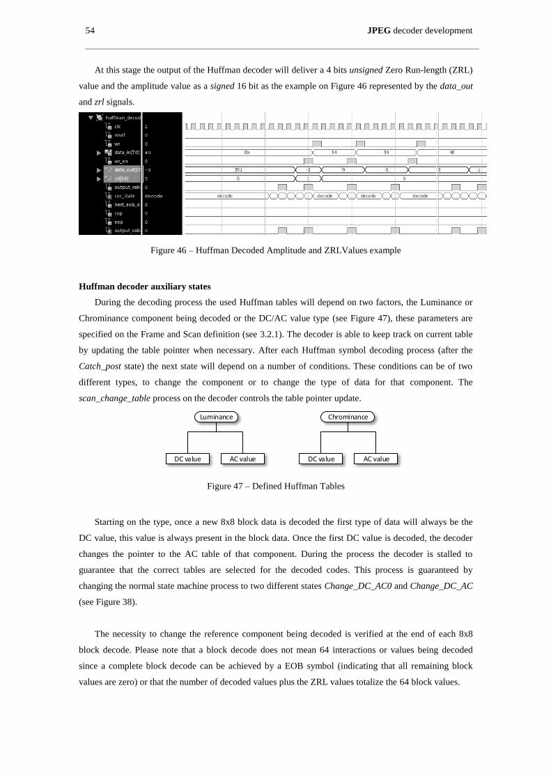
54 JPEG decoder development
At this stage the output of the Huffman decoder will deliver a 4 bits unsigned Zero Run-length (ZRL)
value and the amplitude value as a signed 16 bit as the example on Figure 46 represented by the data_out
and zrl signals.
Figure 46 – Huffman Decoded Amplitude and ZRLValues example
Huffman decoder auxiliary states
During the decoding process the used Huffman tables will depend on two factors, the Luminance or
Chrominance component being decoded or the DC/AC value type (see Figure 47), these parameters are
specified on the Frame and Scan definition (see 3.2.1). The decoder is able to keep track on current table
by updating the table pointer when necessary. After each Huffman symbol decoding process (after the
Catch_post state) the next state will depend on a number of conditions. These conditions can be of two
different types, to change the component or to change the type of data for that component. The
scan_change_table process on the decoder controls the table pointer update.
Luminance Chrominance
DC value AC value DC value AC value
Figure 47 – Defined Huffman Tables
Starting on the type, once a new 8x8 block data is decoded the first type of data will always be the
DC value, this value is always present in the block data. Once the first DC value is decoded, the decoder
changes the pointer to the AC table of that component. During the process the decoder is stalled to
guarantee that the correct tables are selected for the decoded codes. This process is guaranteed by
changing the normal state machine process to two different states Change_DC_AC0 and Change_DC_AC
(see Figure 38).
The necessity to change the reference component being decoded is verified at the end of each 8x8
block decode. Please note that a block decode does not mean 64 interactions or values being decoded
since a complete block decode can be achieved by a EOB symbol (indicating that all remaining block
values are zero) or that the number of decoded values plus the ZRL values totalize the 64 block values.
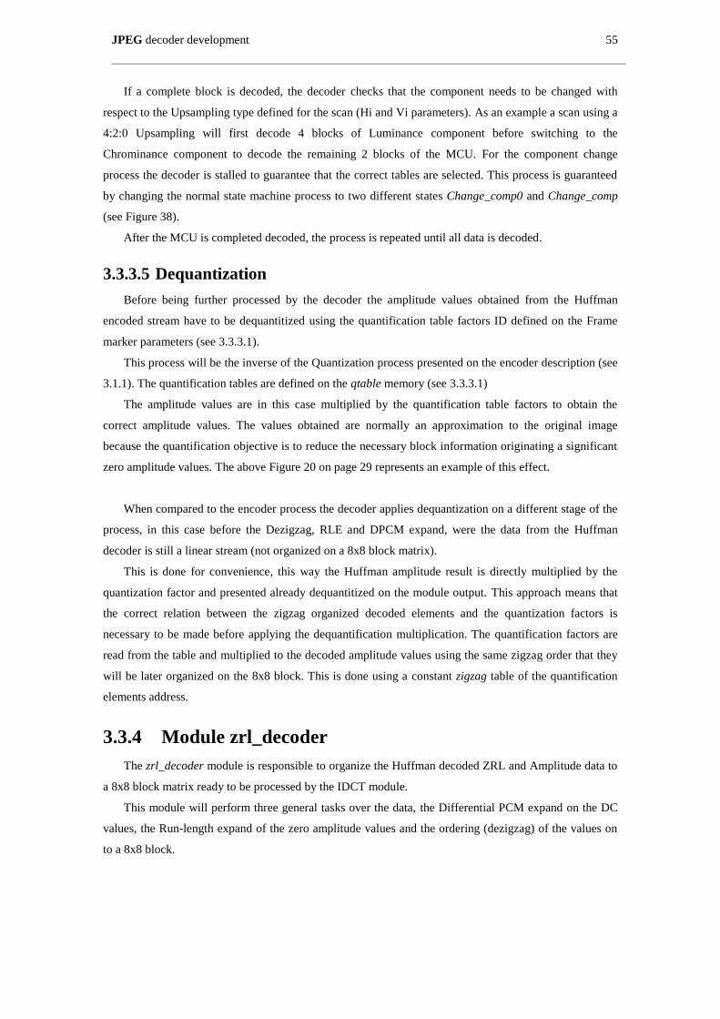
JPEG decoder development 55
If a complete block is decoded, the decoder checks that the component needs to be changed with
respect to the Upsampling type defined for the scan (Hi and Vi parameters). As an example a scan using a
4:2:0 Upsampling will first decode 4 blocks of Luminance component before switching to the
Chrominance component to decode the remaining 2 blocks of the MCU. For the component change
process the decoder is stalled to guarantee that the correct tables are selected. This process is guaranteed
by changing the normal state machine process to two different states Change_comp0 and Change_comp
(see Figure 38).
After the MCU is completed decoded, the process is repeated until all data is decoded.
3.3.3.5 Dequantization
Before being further processed by the decoder the amplitude values obtained from the Huffman
encoded stream have to be dequantitized using the quantification table factors ID defined on the Frame
marker parameters (see 3.3.3.1).
This process will be the inverse of the Quantization process presented on the encoder description (see
3.1.1). The quantification tables are defined on the qtable memory (see 3.3.3.1)
The amplitude values are in this case multiplied by the quantification table factors to obtain the
correct amplitude values. The values obtained are normally an approximation to the original image
because the quantification objective is to reduce the necessary block information originating a significant
zero amplitude values. The above Figure 20 on page 29 represents an example of this effect.
When compared to the encoder process the decoder applies dequantization on a different stage of the
process, in this case before the Dezigzag, RLE and DPCM expand, were the data from the Huffman
decoder is still a linear stream (not organized on a 8x8 block matrix).
This is done for convenience, this way the Huffman amplitude result is directly multiplied by the
quantization factor and presented already dequantitized on the module output. This approach means that
the correct relation between the zigzag organized decoded elements and the quantization factors is
necessary to be made before applying the dequantification multiplication. The quantification factors are
read from the table and multiplied to the decoded amplitude values using the same zigzag order that they
will be later organized on the 8x8 block. This is done using a constant zigzag table of the quantification
elements address.
3.3.4 Module zrl_decoder
The zrl_decoder module is responsible to organize the Huffman decoded ZRL and Amplitude data to
a 8x8 block matrix ready to be processed by the IDCT module.
This module will perform three general tasks over the data, the Differential PCM expand on the DC
values, the Run-length expand of the zero amplitude values and the ordering (dezigzag) of the values on
to a 8x8 block.
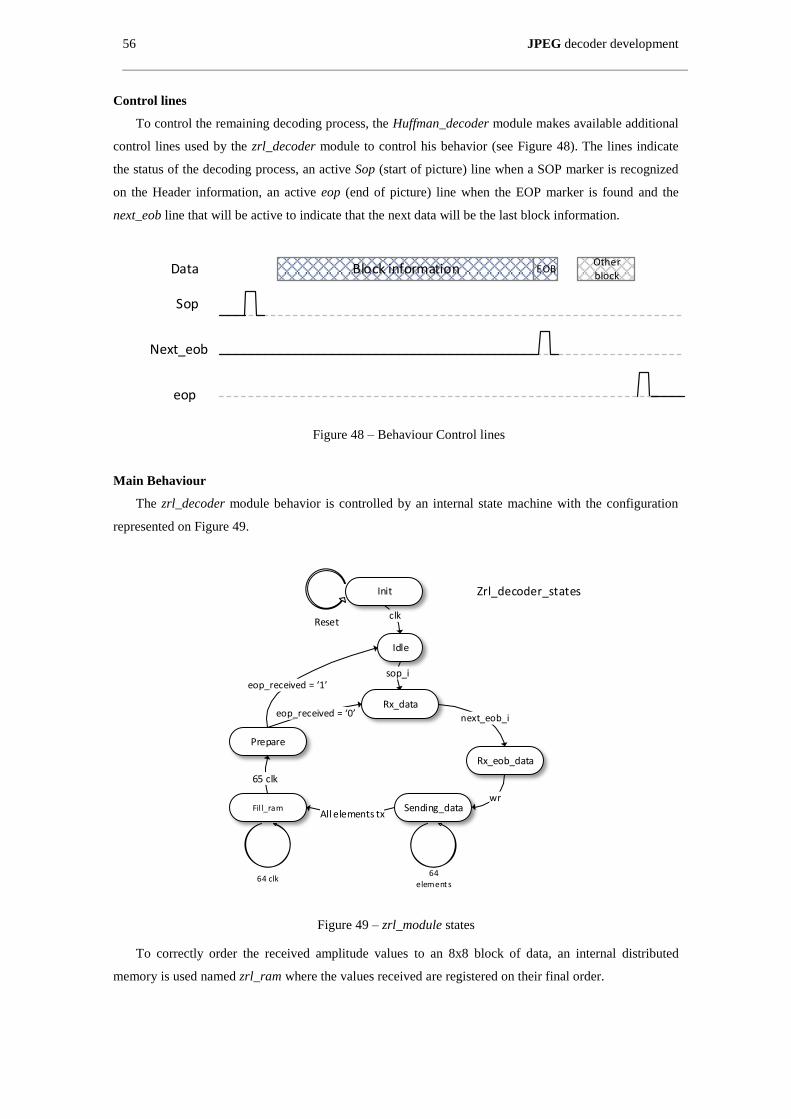
56 JPEG decoder development
Control lines
To control the remaining decoding process, the Huffman_decoder module makes available additional
control lines used by the zrl_decoder module to control his behavior (see Figure 48). The lines indicate
the status of the decoding process, an active Sop (start of picture) line when a SOP marker is recognized
on the Header information, an active eop (end of picture) line when the EOP marker is found and the
next_eob line that will be active to indicate that the next data will be the last block information.
Block informationData
Sop
EOB
Next_eob
eop
Other block
Figure 48 – Behaviour Control lines
Main Behaviour
The zrl_decoder module behavior is controlled by an internal state machine with the configuration
represented on Figure 49.
Rx_data
Rx_eob_data
Idle
sop_i
Sending_dataFil l_ram
Prepare
All elements tx
65 clk
Zrl_decoder_statesInit
Reset
64 elements
64 clk
Figure 49 – zrl_module states
To correctly order the received amplitude values to an 8x8 block of data, an internal distributed
memory is used named zrl_ram where the values received are registered on their final order.
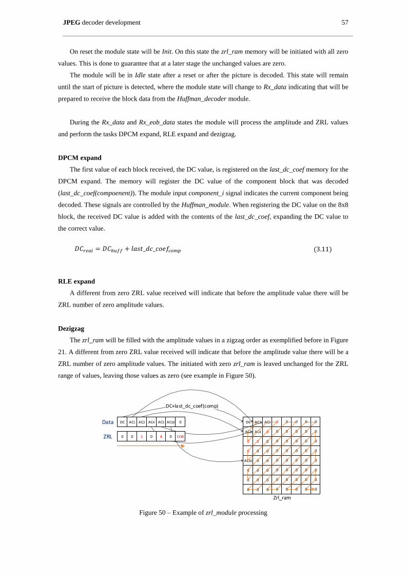
JPEG decoder development 57
On reset the module state will be Init. On this state the zrl_ram memory will be initiated with all zero
values. This is done to guarantee that at a later stage the unchanged values are zero.
The module will be in Idle state after a reset or after the picture is decoded. This state will remain
until the start of picture is detected, where the module state will change to Rx_data indicating that will be
prepared to receive the block data from the Huffman_decoder module.
During the Rx_data and Rx_eob_data states the module will process the amplitude and ZRL values
and perform the tasks DPCM expand, RLE expand and dezigzag.
DPCM expand
The first value of each block received, the DC value, is registered on the last_dc_coef memory for the
DPCM expand. The memory will register the DC value of the component block that was decoded
(last_dc_coef(compoenent)). The module input component_i signal indicates the current component being
decoded. These signals are controlled by the Huffman_module. When registering the DC value on the 8x8
block, the received DC value is added with the contents of the last_dc_coef, expanding the DC value to
the correct value.
(3.11)
RLE expand
A different from zero ZRL value received will indicate that before the amplitude value there will be
ZRL number of zero amplitude values.
Dezigzag
The zrl_ram will be filled with the amplitude values in a zigzag order as exemplified before in Figure
21. A different from zero ZRL value received will indicate that before the amplitude value there will be a
ZRL number of zero amplitude values. The initiated with zero zrl_ram is leaved unchanged for the ZRL
range of values, leaving those values as zero (see example in Figure 50).
Zrl_ram
DC AC1
AC2
0
AC4
DC AC1 AC2 AC4 AC5 AC10 0
0 0 1 0 4 0 EOB
Data
ZRL
AC5 0
0
0
0
0
0
0
0
0
0
0
0
0
0
0
0
0
0
0
0
0
0
0
0
0
0
0
0
0
0
0
0
0
0
0
0
0
0
0
0
0
0
0
0
0
0
0
0
0
0
0
0
0
0
AC10
0
0
0
Figure 50 – Example of zrl_module processing
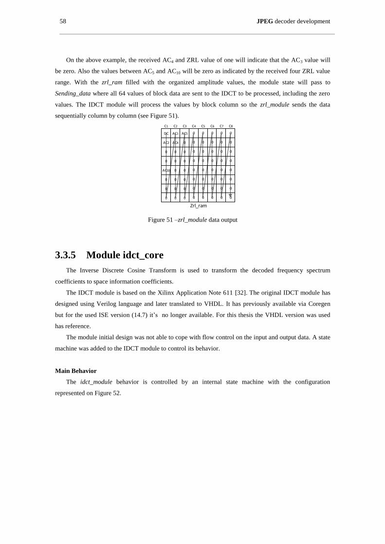
58 JPEG decoder development
On the above example, the received AC4 and ZRL value of one will indicate that the AC3 value will
be zero. Also the values between AC5 and AC10 will be zero as indicated by the received four ZRL value
range. With the zrl_ram filled with the organized amplitude values, the module state will pass to
Sending_data where all 64 values of block data are sent to the IDCT to be processed, including the zero
values. The IDCT module will process the values by block column so the zrl_module sends the data
sequentially column by column (see Figure 51).
Zrl_ram
DC AC1
AC2
0
AC4
AC5 0
0
0
0
0
0
0
0
0
0
0
0
0
0
0
0
0
0
0
0
0
0
0
0
0
0
0
0
0
0
0
0
0
0
0
0
0
0
0
0
0
0
0
0
0
0
0
0
0
0
0
0
0
0
AC10
0
0
0
C1 C2 C3 C4 C5 C6 C7 C8
Figure 51 –zrl_module data output
3.3.5 Module idct_core
The Inverse Discrete Cosine Transform is used to transform the decoded frequency spectrum
coefficients to space information coefficients.
The IDCT module is based on the Xilinx Application Note 611 [32]. The original IDCT module has
designed using Verilog language and later translated to VHDL. It has previously available via Coregen
but for the used ISE version (14.7) it’s no longer available. For this thesis the VHDL version was used
has reference.
The module initial design was not able to cope with flow control on the input and output data. A state
machine was added to the IDCT module to control its behavior.
Main Behavior
The idct_module behavior is controlled by an internal state machine with the configuration
represented on Figure 52.
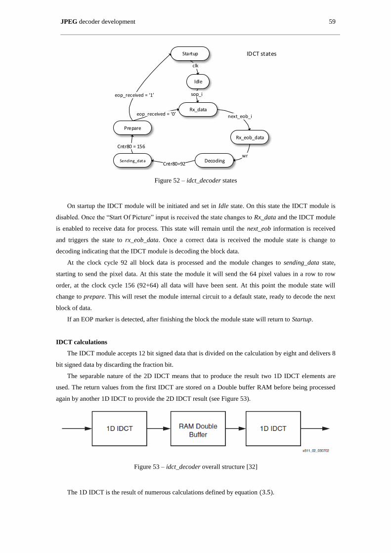
JPEG decoder development 59
Rx_data
Rx_eob_data
Idle
sop_i
DecodingSending_data
Prepare
Cntr80=92
Cntr80 = 156
IDCT statesStartup
Figure 52 – idct_decoder states
On startup the IDCT module will be initiated and set in Idle state. On this state the IDCT module is
disabled. Once the “Start Of Picture” input is received the state changes to Rx_data and the IDCT module
is enabled to receive data for process. This state will remain until the next_eob information is received
and triggers the state to rx_eob_data. Once a correct data is received the module state is change to
decoding indicating that the IDCT module is decoding the block data.
At the clock cycle 92 all block data is processed and the module changes to sending_data state,
starting to send the pixel data. At this state the module it will send the 64 pixel values in a row to row
order, at the clock cycle 156 (92+64) all data will have been sent. At this point the module state will
change to prepare. This will reset the module internal circuit to a default state, ready to decode the next
block of data.
If an EOP marker is detected, after finishing the block the module state will return to Startup.
IDCT calculations
The IDCT module accepts 12 bit signed data that is divided on the calculation by eight and delivers 8
bit signed data by discarding the fraction bit.
The separable nature of the 2D IDCT means that to produce the result two 1D IDCT elements are
used. The return values from the first IDCT are stored on a Double buffer RAM before being processed
again by another 1D IDCT to provide the 2D IDCT result (see Figure 53).
Figure 53 – idct_decoder overall structure [32]
The 1D IDCT is the result of numerous calculations defined by equation (3.5).
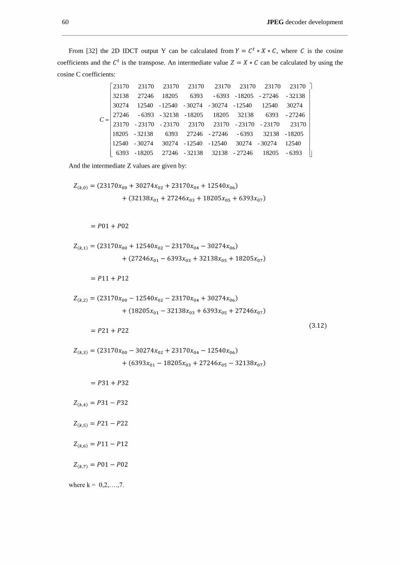
60 JPEG decoder development
From [32] the 2D IDCT output Y can be calculated from , where is the cosine
coefficients and the is the transpose. An intermediate value can be calculated by using the
cosine C coefficients:
6393- 18205 27246- 32138 32138- 27246 18205- 6393
12540 30274- 30274 12540- 12540- 30274 30274- 12540
18205- 32138 6393- 27246- 27246 6393 32138- 18205
23170 23170- 23170- 23170 23170 23170- 23170- 23170
27246- 6393 32138 18205 18205- 32138- 6393- 27246
30274 12540 12540- 30274- 30274- 12540- 12540 30274
32138- 27246- 18205- 6393- 6393 18205 27246 32138
23170 23170 23170 23170 23170 23170 23170 23170
C
And the intermediate Z values are given by:
) )
)
) )
)
) )
)
) )
)
)
)
)
)
(3.12)
where k = 0,2,….,7.
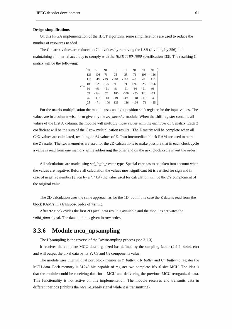
JPEG decoder development 61
Design simplifications
On this FPGA implementation of the IDCT algorithm, some simplifications are used to reduce the
number of resources needed.
The C matrix values are reduced to 7 bit values by removing the LSB (dividing by 256), but
maintaining an internal accuracy to comply with the IEEE 1180-1990 specification [33]. The resulting C
matrix will be the following:
25- 71 106- 126 126- 106 71- 25
49 118- 118 49- 49- 118 118- 49
71- 126 25- 106- 106 25 126- 71
91 91- 91- 91 91 91- 91- 91
106- 25 126 71 71- 126- 25- 106
118 49 49- 118- 118- 49- 49 118
126- 106- 71- 25- 25 71 106 126
91 91 91 91 91 91 91 91
C
For the matrix multiplication the module uses an eight position shift register for the input values. The
values are in a column wise form given by the zrl_decoder module. When the shift register contains all
values of the first X column, the module will multiply those values with the each row of C matrix. Each Z
coefficient will be the sum of the C row multiplication results.. The Z matrix will be complete when all
C*X values are calculated, resulting on 64 values of Z. Two intermediate block RAM are used to store
the Z results. The two memories are used for the 2D calculations to make possible that in each clock cycle
a value is read from one memory while addressing the other and on the next clock cycle invert the order.
All calculations are made using std_logic_vector type. Special care has to be taken into account when
the values are negative. Before all calculation the values most significant bit is verified for sign and in
case of negative number (given by a ‘1’ bit) the value used for calculation will be the 2’s complement of
the original value.
The 2D calculation uses the same approach as for the 1D, but in this case the Z data is read from the
block RAM’s in a transpose order of writing.
After 92 clock cycles the first 2D pixel data result is available and the modules activates the
valid_data signal. The data output is given in row order.
3.3.6 Module mcu_upsampling
The Upsampling is the reverse of the Downsampling process (see 3.1.3).
It receives the complete MCU data organized has defined by the sampling factor (4:2:2, 4:4:4, etc)
and will output the pixel data by its Y, CB and CR components value.
The module uses internal dual port block memories Y_buffer, Cb_buffer and Cr_buffer to register the
MCU data. Each memory is 512x8 bits capable of register two complete 16x16 size MCU. The idea is
that the module could be receiving data for a MCU and delivering the previous MCU reorganized data.
This functionality is not active on this implementation. The module receives and transmits data in
different periods (inhibits the receive_ready signal while it is transmitting).
62 JPEG decoder development
The module receives the MCU data together with the sampling factor used. Depending on the
sampling the data received will be organized as defined on Table 2. The block information will be
received from left to right and top to bottom order. At the output the modules deliver the MCU pixel data
on the same order.
During the MCU data receiving, an input counter counter_in is used to control the RAM write and
addresses lines according to the sampling factor. As an example for a 4:2:0 sampling factor the module
expects a total of 384 (6*64) input values. The values are from received data 1 to 256 the Y component
data, from 257 to 320 the CB component data and 321 to 384 the CR component data. For all sampling
factors the component memory write address will be organized according to Figure 54:
Counter_in[5:3]
Y1
Counter_in[2:0] 700
7
Counter_in[5:3]
Y2
Counter_in[2:0] 700
7
Counter_in[5:3]
Y3
Counter_in[2:0] 700
7
Counter_in[5:3]
Y4
Counter_in[2:0] 700
7
Counter_in[7:6]
0
1
2
3
Counter_in[5:3]
Cb
Counter_in[2:0] 700
7
Counter_in[5:3]
Cr
Counter_in[2:0] 700
7
Counter_in[8]
1
Counter_in[8]
&
Counter_in[6]
1
Figure 54 – MCU_upsampling component memory write structure (for 4:2:0
sampling)
After all MCU data is received the module changes to transmit state and an output counter
counter_out is used to control each RAM read address according to the used sampling factor. As an
example for a 4:2:0 sampling factor the module will deliver a total of 256 (16*16) output component
values. For the 4:2:0 sampling factor the component memory read address will be organized according to
Figure 55:
JPEG decoder development 63
Counter_out[6:4]
Y1
Counter_out[2:0] 700
7
Counter_out[6:4]
Y2
Counter_out[2:0] 700
7
Counter_out[6:4]
Y3
Counter_out[2:0] 700
7
Counter_out[6:4]
Y4
Counter_out[2:0] 700
7
Counter_out[7]
&
Counter_out[3]
0
1
2
3
Counter_out[7:5]
Cb
Counter_out[3:1] 700
7
Counter_out[7:5]
Cr
Counter_out[3:1] 700
7
Figure 55 – MCU_upsampling component memory read structure (for 4:2:0
sampling)
3.3.7 Module YCbCr2RGB
The output of the JPEG decoder is in RGB color space. The decoder internal Y, CB, CR is
transformed to RGB using the equations defined in [28]:
( ))) ) (3.13)
( ) )))) ) (3.14)
( )) ) (3.15)
The IDCT values are level shifted, this means that 128 is subtracted from the values. The module will
level the IDCT and use the defined formulas multiplied by 1024 (10 bit shift right) and with the factors
rounded to the next integer. Resulting on the following formulas applied:
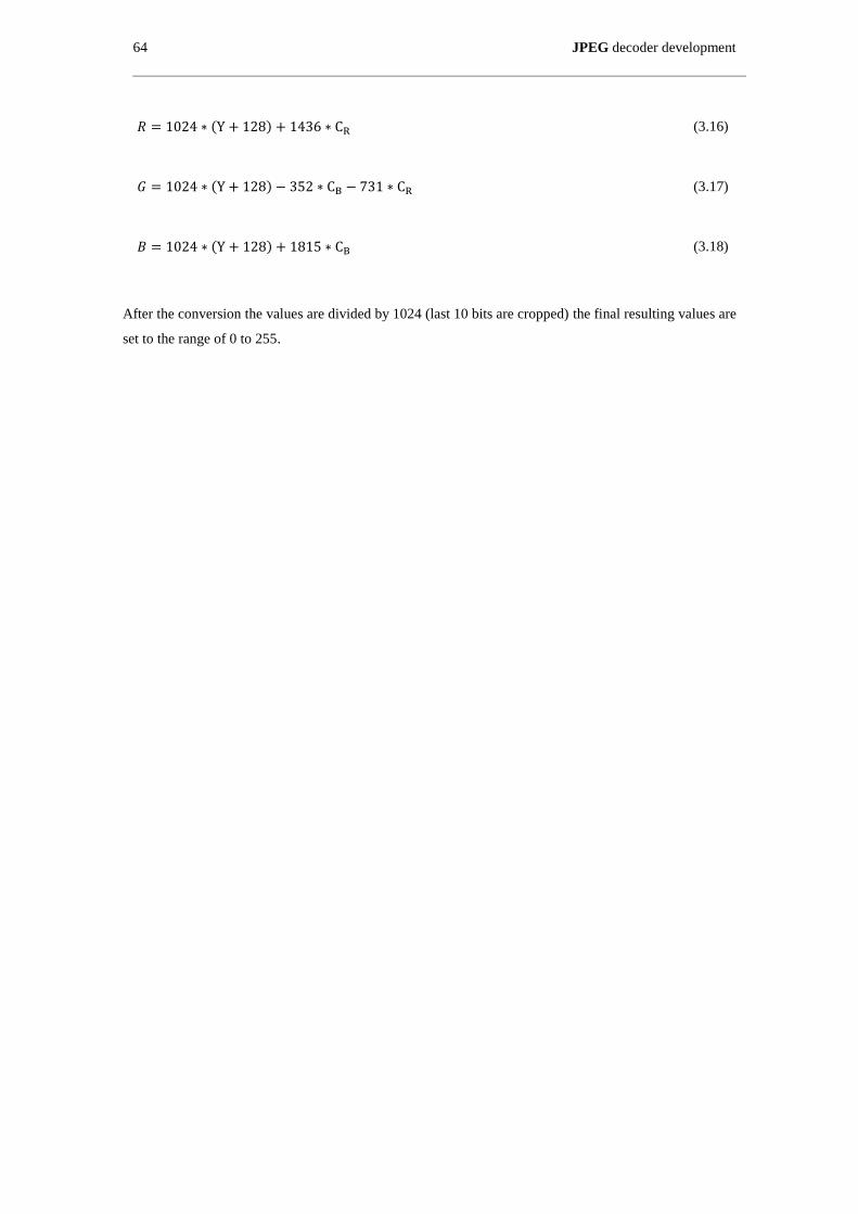
64 JPEG decoder development
) (3.16)
) (3.17)
) (3.18)
After the conversion the values are divided by 1024 (last 10 bits are cropped) the final resulting values are
set to the range of 0 to 255.
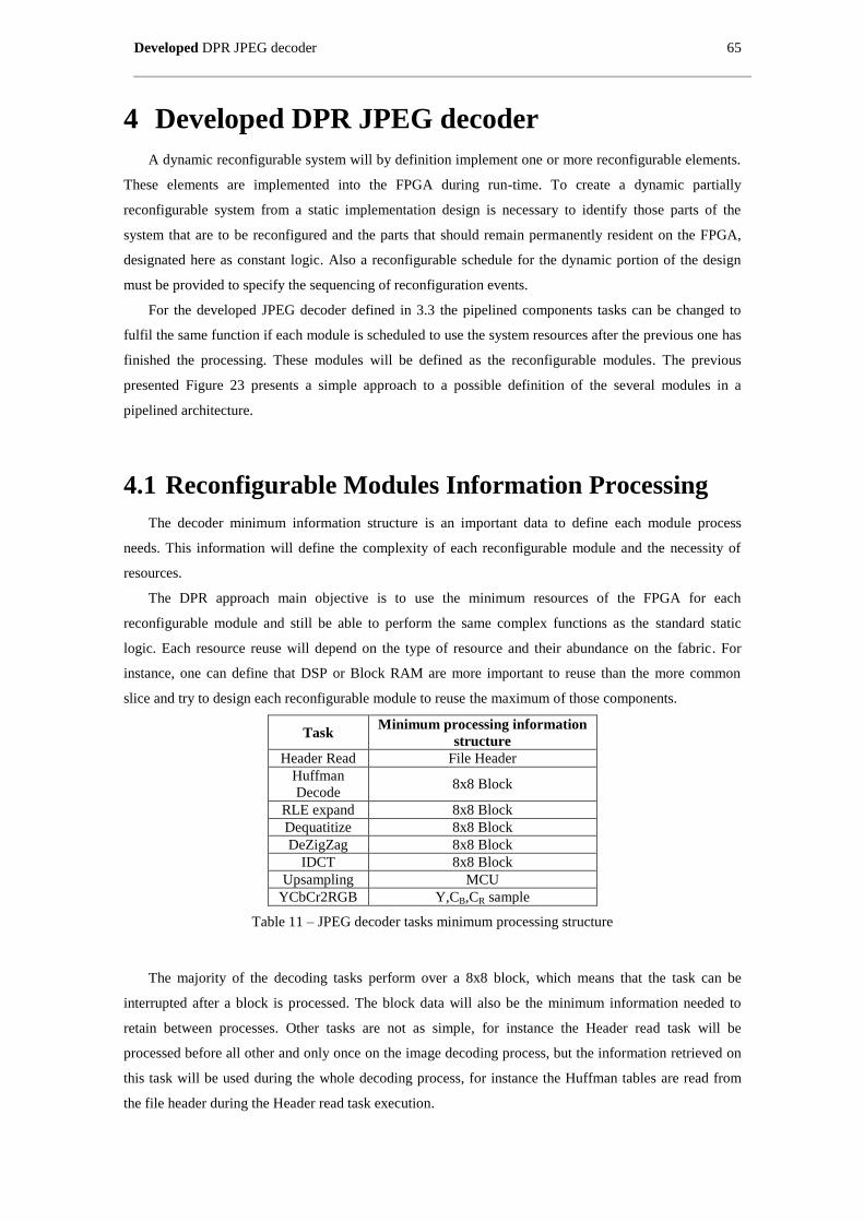
Developed DPR JPEG decoder 65
4 Developed DPR JPEG decoder
A dynamic reconfigurable system will by definition implement one or more reconfigurable elements.
These elements are implemented into the FPGA during run-time. To create a dynamic partially
reconfigurable system from a static implementation design is necessary to identify those parts of the
system that are to be reconfigured and the parts that should remain permanently resident on the FPGA,
designated here as constant logic. Also a reconfigurable schedule for the dynamic portion of the design
must be provided to specify the sequencing of reconfiguration events.
For the developed JPEG decoder defined in 3.3 the pipelined components tasks can be changed to
fulfil the same function if each module is scheduled to use the system resources after the previous one has
finished the processing. These modules will be defined as the reconfigurable modules. The previous
presented Figure 23 presents a simple approach to a possible definition of the several modules in a
pipelined architecture.
4.1 Reconfigurable Modules Information Processing
The decoder minimum information structure is an important data to define each module process
needs. This information will define the complexity of each reconfigurable module and the necessity of
resources.
The DPR approach main objective is to use the minimum resources of the FPGA for each
reconfigurable module and still be able to perform the same complex functions as the standard static
logic. Each resource reuse will depend on the type of resource and their abundance on the fabric. For
instance, one can define that DSP or Block RAM are more important to reuse than the more common
slice and try to design each reconfigurable module to reuse the maximum of those components.
Task Minimum processing information
structure
Header Read File Header
Huffman
Decode 8x8 Block
RLE expand 8x8 Block
Dequatitize 8x8 Block
DeZigZag 8x8 Block
IDCT 8x8 Block
Upsampling MCU
YCbCr2RGB Y,CB,CR sample
Table 11 – JPEG decoder tasks minimum processing structure
The majority of the decoding tasks perform over a 8x8 block, which means that the task can be
interrupted after a block is processed. The block data will also be the minimum information needed to
retain between processes. Other tasks are not as simple, for instance the Header read task will be
processed before all other and only once on the image decoding process, but the information retrieved on
this task will be used during the whole decoding process, for instance the Huffman tables are read from
the file header during the Header read task execution.
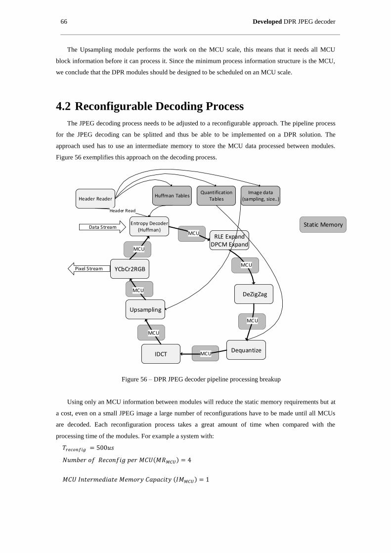
66 Developed DPR JPEG decoder
The Upsampling module performs the work on the MCU scale, this means that it needs all MCU
block information before it can process it. Since the minimum process information structure is the MCU,
we conclude that the DPR modules should be designed to be scheduled on an MCU scale.
4.2 Reconfigurable Decoding Process
The JPEG decoding process needs to be adjusted to a reconfigurable approach. The pipeline process
for the JPEG decoding can be splitted and thus be able to be implemented on a DPR solution. The
approach used has to use an intermediate memory to store the MCU data processed between modules.
Figure 56 exemplifies this approach on the decoding process.
DeZigZag
IDCT
Header Reader
Entropy Decoder(Huffman)
Quantification Tables
Huffman Tables
RLE ExpandDPCM Expand
Dequantize
Upsampling
YCbCr2RGB
Data Stream
Image data(sampling, size..)
Static Memory
Figure 56 – DPR JPEG decoder pipeline processing breakup
Using only an MCU information between modules will reduce the static memory requirements but at
a cost, even on a small JPEG image a large number of reconfigurations have to be made until all MCUs
are decoded. Each reconfiguration process takes a great amount of time when compared with the
processing time of the modules. For example a system with:
)
)
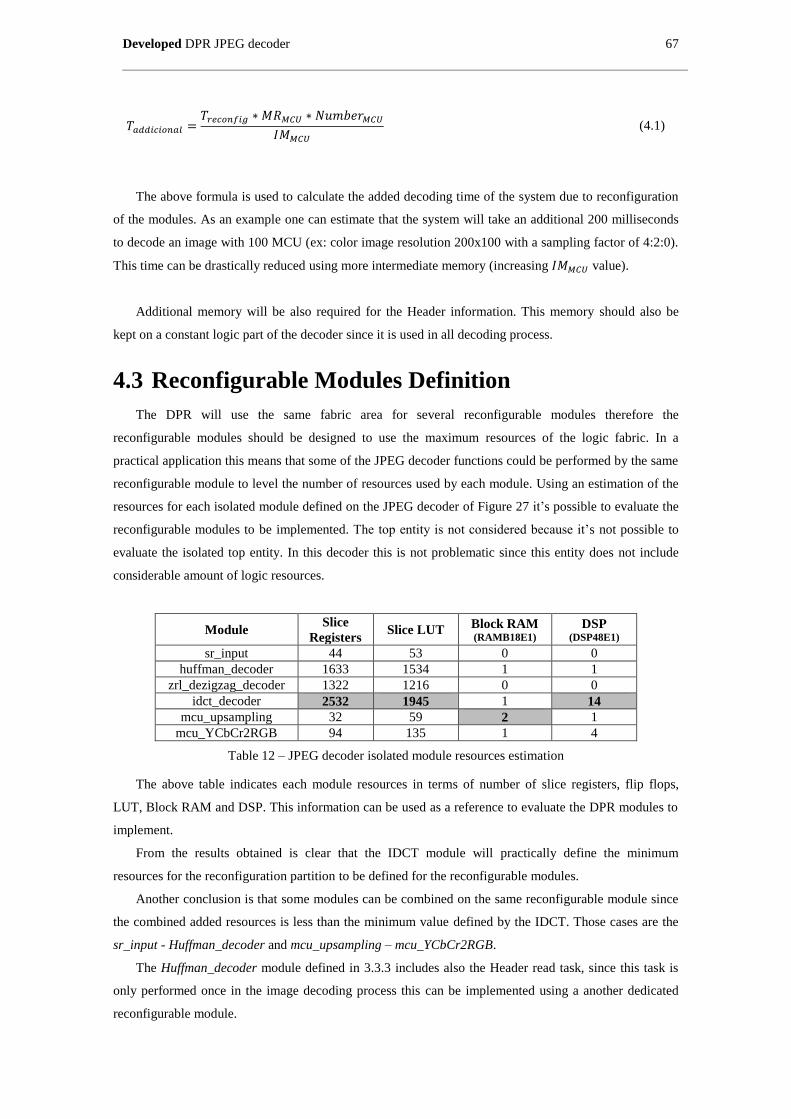
Developed DPR JPEG decoder 67
(4.1)
The above formula is used to calculate the added decoding time of the system due to reconfiguration
of the modules. As an example one can estimate that the system will take an additional 200 milliseconds
to decode an image with 100 MCU (ex: color image resolution 200x100 with a sampling factor of 4:2:0).
This time can be drastically reduced using more intermediate memory (increasing value).
Additional memory will be also required for the Header information. This memory should also be
kept on a constant logic part of the decoder since it is used in all decoding process.
4.3 Reconfigurable Modules Definition
The DPR will use the same fabric area for several reconfigurable modules therefore the
reconfigurable modules should be designed to use the maximum resources of the logic fabric. In a
practical application this means that some of the JPEG decoder functions could be performed by the same
reconfigurable module to level the number of resources used by each module. Using an estimation of the
resources for each isolated module defined on the JPEG decoder of Figure 27 it’s possible to evaluate the
reconfigurable modules to be implemented. The top entity is not considered because it’s not possible to
evaluate the isolated top entity. In this decoder this is not problematic since this entity does not include
considerable amount of logic resources.
Module Slice
Registers Slice LUT
Block RAM (RAMB18E1)
DSP (DSP48E1)
sr_input 44 53 0 0
huffman_decoder 1633 1534 1 1
zrl_dezigzag_decoder 1322 1216 0 0
idct_decoder 2532 1945 1 14
mcu_upsampling 32 59 2 1
mcu_YCbCr2RGB 94 135 1 4
Table 12 – JPEG decoder isolated module resources estimation
The above table indicates each module resources in terms of number of slice registers, flip flops,
LUT, Block RAM and DSP. This information can be used as a reference to evaluate the DPR modules to
implement.
From the results obtained is clear that the IDCT module will practically define the minimum
resources for the reconfiguration partition to be defined for the reconfigurable modules.
Another conclusion is that some modules can be combined on the same reconfigurable module since
the combined added resources is less than the minimum value defined by the IDCT. Those cases are the
sr_input - Huffman_decoder and mcu_upsampling – mcu_YCbCr2RGB.
The Huffman_decoder module defined in 3.3.3 includes also the Header read task, since this task is
only performed once in the image decoding process this can be implemented using a another dedicated
reconfigurable module.
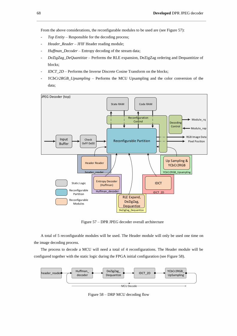
68 Developed DPR JPEG decoder
From the above considerations, the reconfigurable modules to be used are (see Figure 57):
- Top Entity – Responsible for the decoding process;
- Header_Reader – JFIF Header reading module;
- Huffman_Decoder – Entropy decoding of the stream data;
- DeZigZag_DeQuantitize – Performs the RLE expansion, DeZigZag ordering and Dequantitize of
blocks;
- IDCT_2D – Performs the Inverse Discrete Cosine Transform on the blocks;
- YCbCr2RGB_Upsampling – Performs the MCU Upsampling and the color conversion of the
data;
JPEG Decoder (top)
Input Buffer
Check0xFF 0x00
Entropy Decoder (Huffman)
RLE Expand, DeZigZag,
Dequantize
IDCT
Up Sampling & YCbCr2RGB
Reconfigurable Partition
Header Reader
State RAM Code RAM
Static Logic
Reconfigurable Partition
Reconfigurable Modules
RGB Image Data
header_reader YCbCr2RGB_Upsampling
IDCT_2D
DeZigZag_Dequantize
Huffman_decoder
Decoding Control
Reconfiguration Control
Module_rq
Pixel Position
Module_rep
Figure 57 – DPR JPEG decoder overall architecture
A total of 5 reconfigurable modules will be used. The Header module will only be used one time on
the image decoding process.
The process to decode a MCU will need a total of 4 reconfigurations. The Header module will be
configured together with the static logic during the FPGA initial configuration (see Figure 58).
header_readerHuffman_decoder
DeZigZag_Dequantize
IDCT_2DYCbCr2RGB_UpSampling
MCU Decode
Figure 58 – DRP MCU decoding flow
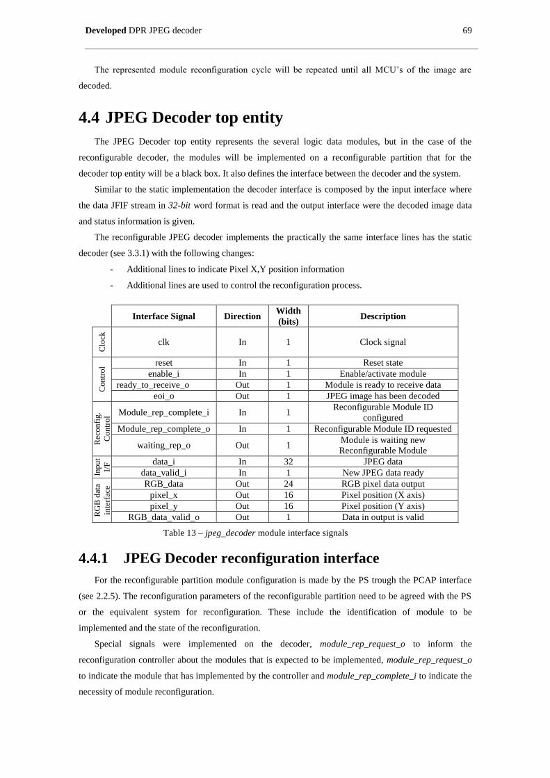
Developed DPR JPEG decoder 69
The represented module reconfiguration cycle will be repeated until all MCU’s of the image are
decoded.
4.4 JPEG Decoder top entity
The JPEG Decoder top entity represents the several logic data modules, but in the case of the
reconfigurable decoder, the modules will be implemented on a reconfigurable partition that for the
decoder top entity will be a black box. It also defines the interface between the decoder and the system.
Similar to the static implementation the decoder interface is composed by the input interface where
the data JFIF stream in 32-bit word format is read and the output interface were the decoded image data
and status information is given.
The reconfigurable JPEG decoder implements the practically the same interface lines has the static
decoder (see 3.3.1) with the following changes:
- Additional lines to indicate Pixel X,Y position information
- Additional lines are used to control the reconfiguration process.
Interface Signal Direction
Width
(bits) Description
Clo
ck
clk In 1 Clock signal
Co
ntr
ol reset In 1 Reset state
enable_i In 1 Enable/activate module
ready_to_receive_o Out 1 Module is ready to receive data
eoi_o Out 1 JPEG image has been decoded
Rec
on
fig
.
Co
ntr
ol Module_rep_complete_i In 1
Reconfigurable Module ID
configured
Module_rep_complete_o In 1 Reconfigurable Module ID requested
waiting_rep_o Out 1 Module is waiting new
Reconfigurable Module
Inpu
t
I/F
data_i In 32 JPEG data
data_valid_i In 1 New JPEG data ready
RG
B d
ata
inte
rfac
e RGB_data Out 24 RGB pixel data output
pixel_x Out 16 Pixel position (X axis)
pixel_y Out 16 Pixel position (Y axis)
RGB_data_valid_o Out 1 Data in output is valid
Table 13 – jpeg_decoder module interface signals
4.4.1 JPEG Decoder reconfiguration interface
For the reconfigurable partition module configuration is made by the PS trough the PCAP interface
(see 2.2.5). The reconfiguration parameters of the reconfigurable partition need to be agreed with the PS
or the equivalent system for reconfiguration. These include the identification of module to be
implemented and the state of the reconfiguration.
Special signals were implemented on the decoder, module_rep_request_o to inform the
reconfiguration controller about the modules that is expected to be implemented, module_rep_request_o
to indicate the module that has implemented by the controller and module_rep_complete_i to indicate the
necessity of module reconfiguration.
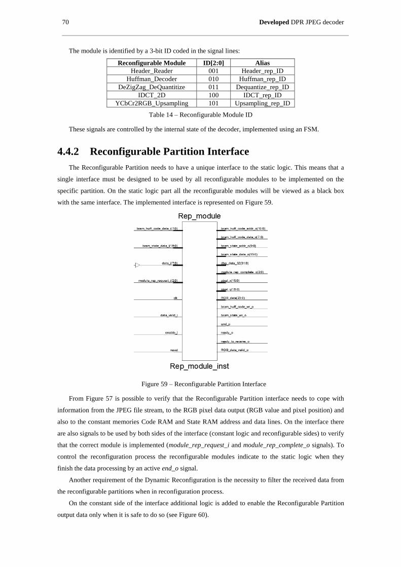
70 Developed DPR JPEG decoder
The module is identified by a 3-bit ID coded in the signal lines:
Reconfigurable Module ID[2:0] Alias
Header_Reader 001 Header_rep_ID
Huffman_Decoder 010 Huffman_rep_ID
DeZigZag_DeQuantitize 011 Dequantize_rep_ID
IDCT_2D 100 IDCT_rep_ID
YCbCr2RGB_Upsampling 101 Upsampling_rep_ID
Table 14 – Reconfigurable Module ID
These signals are controlled by the internal state of the decoder, implemented using an FSM.
4.4.2 Reconfigurable Partition Interface
The Reconfigurable Partition needs to have a unique interface to the static logic. This means that a
single interface must be designed to be used by all reconfigurable modules to be implemented on the
specific partition. On the static logic part all the reconfigurable modules will be viewed as a black box
with the same interface. The implemented interface is represented on Figure 59.
Figure 59 – Reconfigurable Partition Interface
From Figure 57 is possible to verify that the Reconfigurable Partition interface needs to cope with
information from the JPEG file stream, to the RGB pixel data output (RGB value and pixel position) and
also to the constant memories Code RAM and State RAM address and data lines. On the interface there
are also signals to be used by both sides of the interface (constant logic and reconfigurable sides) to verify
that the correct module is implemented (module_rep_request_i and module_rep_complete_o signals). To
control the reconfiguration process the reconfigurable modules indicate to the static logic when they
finish the data processing by an active end_o signal.
Another requirement of the Dynamic Reconfiguration is the necessity to filter the received data from
the reconfigurable partitions when in reconfiguration process.
On the constant side of the interface additional logic is added to enable the Reconfigurable Partition
output data only when it is safe to do so (see Figure 60).
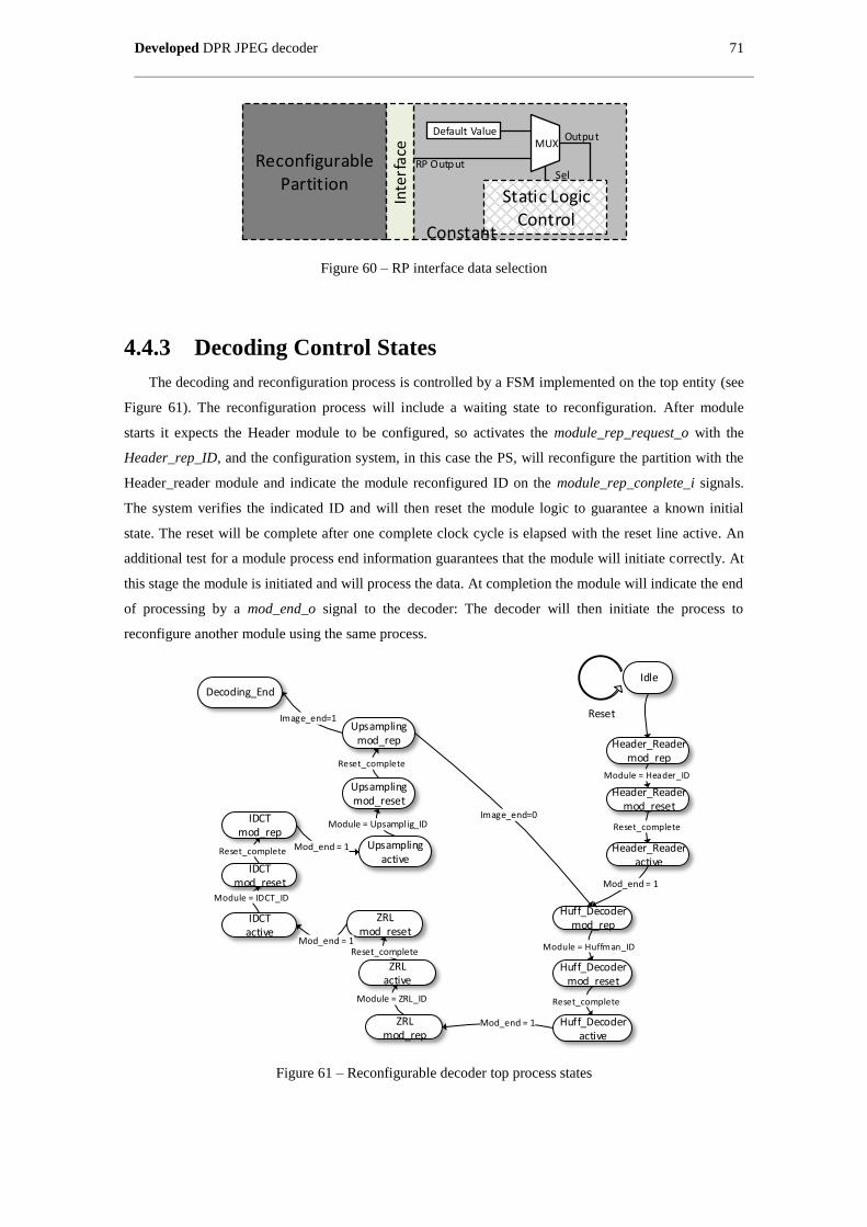
Developed DPR JPEG decoder 71
Reconfigurable Partition
MUXDefault Value Output
Sel
Inte
rfac
e
RP Output
Static Logic Control
Constant
Figure 60 – RP interface data selection
4.4.3 Decoding Control States
The decoding and reconfiguration process is controlled by a FSM implemented on the top entity (see
Figure 61). The reconfiguration process will include a waiting state to reconfiguration. After module
starts it expects the Header module to be configured, so activates the module_rep_request_o with the
Header_rep_ID, and the configuration system, in this case the PS, will reconfigure the partition with the
Header_reader module and indicate the module reconfigured ID on the module_rep_conplete_i signals.
The system verifies the indicated ID and will then reset the module logic to guarantee a known initial
state. The reset will be complete after one complete clock cycle is elapsed with the reset line active. An
additional test for a module process end information guarantees that the module will initiate correctly. At
this stage the module is initiated and will process the data. At completion the module will indicate the end
of processing by a mod_end_o signal to the decoder: The decoder will then initiate the process to
reconfigure another module using the same process.
Idle
Module = Header_ID
Header_Readermod_rep
Header_Readermod_reset
Header_Readeractive
Huff_Decodermod_rep
Huff_Decodermod_reset
Huff_Decoderactive
ZRLmod_rep
ZRLmod_reset
ZRLactive
IDCTmod_rep
IDCTmod_reset
IDCTactive
Upsamplingmod_rep
Upsamplingmod_reset
Upsamplingactive
Decoding_End
Reset
Reset_complete
Module = Huffman_ID
Reset_complete
Module = IDCT_ID
Reset_complete
Reset_complete
Figure 61 – Reconfigurable decoder top process states
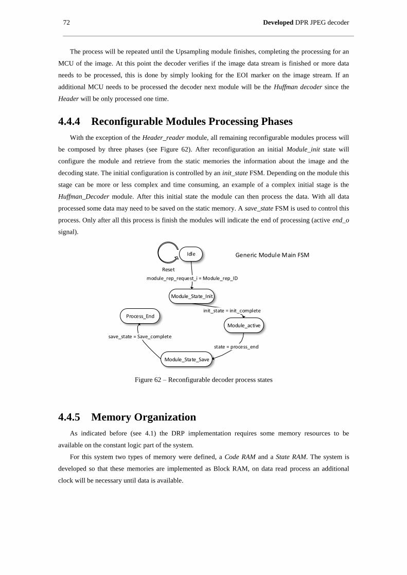
72 Developed DPR JPEG decoder
The process will be repeated until the Upsampling module finishes, completing the processing for an
MCU of the image. At this point the decoder verifies if the image data stream is finished or more data
needs to be processed, this is done by simply looking for the EOI marker on the image stream. If an
additional MCU needs to be processed the decoder next module will be the Huffman decoder since the
Header will be only processed one time.
4.4.4 Reconfigurable Modules Processing Phases
With the exception of the Header_reader module, all remaining reconfigurable modules process will
be composed by three phases (see Figure 62). After reconfiguration an initial Module_init state will
configure the module and retrieve from the static memories the information about the image and the
decoding state. The initial configuration is controlled by an init_state FSM. Depending on the module this
stage can be more or less complex and time consuming, an example of a complex initial stage is the
Huffman_Decoder module. After this initial state the module can then process the data. With all data
processed some data may need to be saved on the static memory. A save_state FSM is used to control this
process. Only after all this process is finish the modules will indicate the end of processing (active end_o
signal).
Module_State_Init
Module_active
Idle
Module_State_Save
Process_End
Generic Module Main FSM
Reset
Figure 62 – Reconfigurable decoder process states
4.4.5 Memory Organization
As indicated before (see 4.1) the DRP implementation requires some memory resources to be
available on the constant logic part of the system.
For this system two types of memory were defined, a Code RAM and a State RAM. The system is
developed so that these memories are implemented as Block RAM, on data read process an additional
clock will be necessary until data is available.
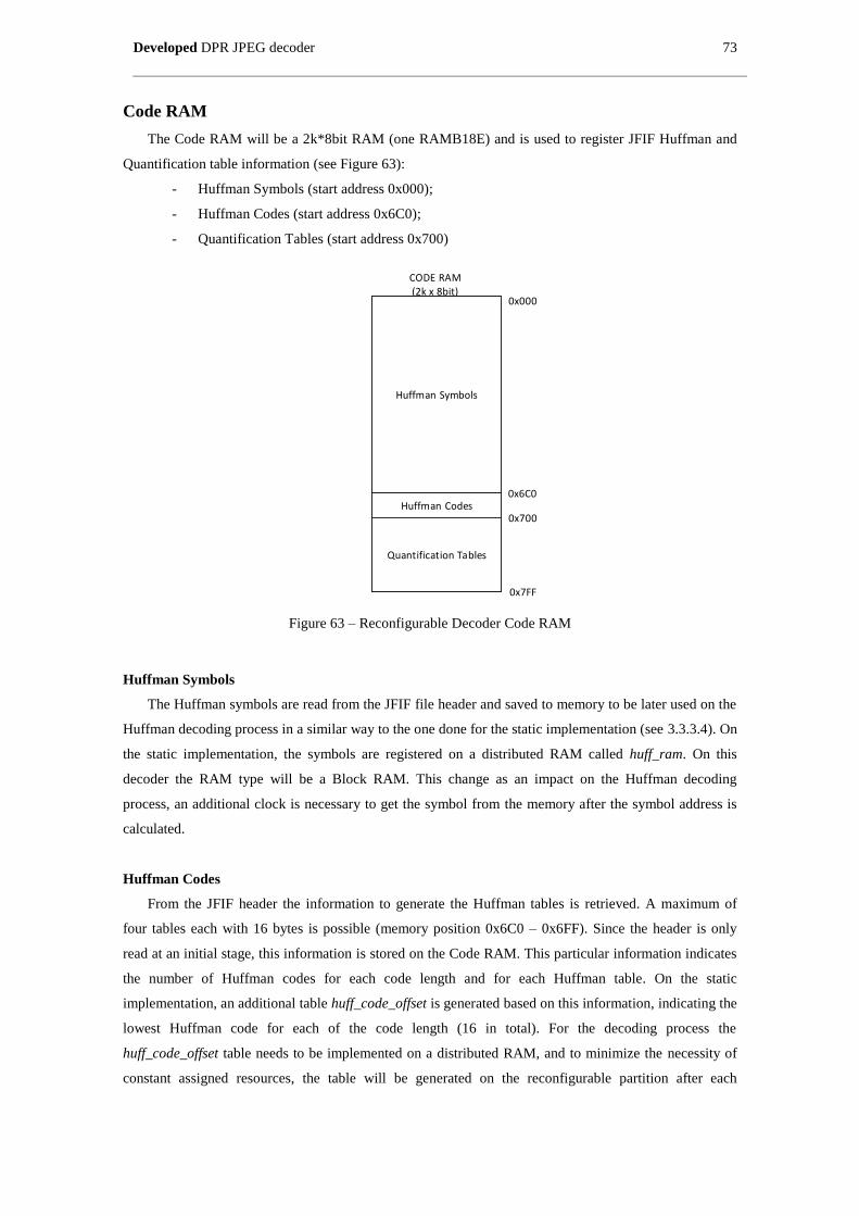
Developed DPR JPEG decoder 73
Code RAM
The Code RAM will be a 2k*8bit RAM (one RAMB18E) and is used to register JFIF Huffman and
Quantification table information (see Figure 63):
- Huffman Symbols (start address 0x000);
- Huffman Codes (start address 0x6C0);
- Quantification Tables (start address 0x700)
0x000
CODE RAM(2k x 8bit)
0x7FF
Huffman Symbols
Huffman Codes0x6C0
0x700
Quantification Tables
Figure 63 – Reconfigurable Decoder Code RAM
Huffman Symbols
The Huffman symbols are read from the JFIF file header and saved to memory to be later used on the
Huffman decoding process in a similar way to the one done for the static implementation (see 3.3.3.4). On
the static implementation, the symbols are registered on a distributed RAM called huff_ram. On this
decoder the RAM type will be a Block RAM. This change as an impact on the Huffman decoding
process, an additional clock is necessary to get the symbol from the memory after the symbol address is
calculated.
Huffman Codes
From the JFIF header the information to generate the Huffman tables is retrieved. A maximum of
four tables each with 16 bytes is possible (memory position 0x6C0 – 0x6FF). Since the header is only
read at an initial stage, this information is stored on the Code RAM. This particular information indicates
the number of Huffman codes for each code length and for each Huffman table. On the static
implementation, an additional table huff_code_offset is generated based on this information, indicating the
lowest Huffman code for each of the code length (16 in total). For the decoding process the
huff_code_offset table needs to be implemented on a distributed RAM, and to minimize the necessity of
constant assigned resources, the table will be generated on the reconfigurable partition after each
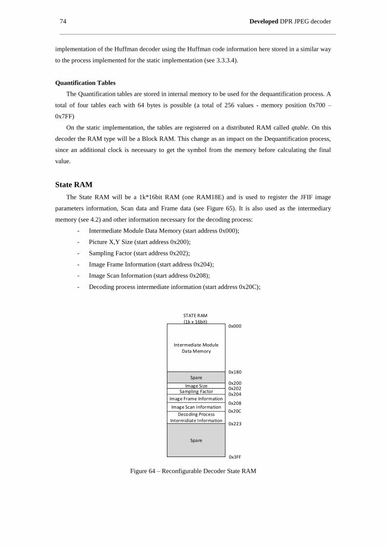
74 Developed DPR JPEG decoder
implementation of the Huffman decoder using the Huffman code information here stored in a similar way
to the process implemented for the static implementation (see 3.3.3.4).
Quantification Tables
The Quantification tables are stored in internal memory to be used for the dequantification process. A
total of four tables each with 64 bytes is possible (a total of 256 values - memory position 0x700 –
0x7FF)
On the static implementation, the tables are registered on a distributed RAM called qtable. On this
decoder the RAM type will be a Block RAM. This change as an impact on the Dequantification process,
since an additional clock is necessary to get the symbol from the memory before calculating the final
value.
State RAM
The State RAM will be a 1k*16bit RAM (one RAM18E) and is used to register the JFIF image
parameters information, Scan data and Frame data (see Figure 65). It is also used as the intermediary
memory (see 4.2) and other information necessary for the decoding process:
- Intermediate Module Data Memory (start address 0x000);
- Picture X,Y Size (start address 0x200);
- Sampling Factor (start address 0x202);
- Image Frame Information (start address 0x204);
- Image Scan Information (start address 0x208);
- Decoding process intermediate information (start address 0x20C);
0x000
STATE RAM(1k x 16bit)
0x3FF
Intermediate Module Data Memory
Image Size0x200
0x20CDecoding Process
Intermidiate Information
Sampling Factor0x202
Image Frame Information
Image Scan Information
0x204
0x208
Spare
Spare0x180
0x223
Figure 64 – Reconfigurable Decoder State RAM
Developed DPR JPEG decoder 75
Intermediate Module Data Memory
This RAM area is used to register the information processed by each reconfigurable module during
the decoding process. All modules share this region of memory thus the information that it contains will
vary with the decoding stage. As referred in 4.2 the memory capacity has to be one MCU. The memory
region is prepared for the JPEG standard worst case scenario, which for images using the 4:2:0 sampling
factor it needs to hold six 8x8 blocks element information (a total of 384 elements). The size of each
element varies. The worst case are the Huffman decoded elements that are composed by the 12bit
amplitude value for the IDCT and the 4 bit ZRL value, giving a total of 16 bits of information for each
element. To simplify the implementation, the 16 bits memory organization registers the 16 bit ZRL and
amplitude value for each element.
The memory is arranged in blocks for each component. For the Luminance component, a total of four
blocks are defined;
Block Y1 – Defined from 0x000 to 0x03F
Block Y2 – Defined from 0x040 to 0x07F
Block Y3 – Defined from 0x080 to 0x0BF
Block Y4 – Defined from 0x0C0 to 0x0FF
For the Chrominance components, a total of two blocks are defined;
Block CB – Defined from 0x100 to 0x13F
Block CR – Defined from 0x140 to 0x17F
Until the block data is expanded, by the Dezigzag_Dequantitize module, each block of data can be
represented by less than 64 elements. Each module needs to keep track on the remaining and already
decoded elements.
Image Size
This RAM area is used to register of the information retrieved on the JFIF for the image Y and X
pixel size. Each element is a 16 bit value so the memory will contain:
Image Y size – Defined on address 0x200
Image X size – Defined on address 0x201
Sampling Factor
This RAM area is used to register of the information retrieved on the JFIF for the image Sampling
Factor. The memory will contain the Sampling Factor in a reduced form has defined in 0:
Sampling Factor – Defined on address 0x202
Image Frame Information
The image Frame information as it is defined in the JFIF header is stored on this RAM area. It will
contain a maximum of 3 components information on the following positions:
Number of Frame Components – Defined on address 0x204
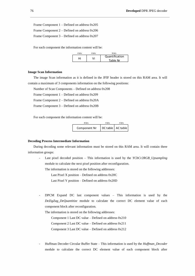
76 Developed DPR JPEG decoder
Frame Component 1 – Defined on address 0x205
Frame Component 2 – Defined on address 0x206
Frame Component 3 – Defined on address 0x207
For each component the information content will be:
Hi ViQuantification
Table Nr
4 bits 4 bits 8 bits
Image Scan Information
The image Scan information as it is defined in the JFIF header is stored on this RAM area. It will
contain a maximum of 3 components information on the following positions:
Number of Scan Components – Defined on address 0x208
Frame Component 1 – Defined on address 0x209
Frame Component 2 – Defined on address 0x20A
Frame Component 3 – Defined on address 0x20B
For each component the information content will be:
DC table AC tableComponent Nr
4 bits 4 bits8 bits
Decoding Process Intermediate Information
During decoding some relevant information must be stored on this RAM area. It will contain three
information groups:
- Last pixel decoded position – This information is used by the YCbCr2RGB_Upsampling
module to calculate the next pixel position after reconfiguration.
The information is stored on the following addresses:
Last Pixel X position – Defined on address 0x20C
Last Pixel Y position – Defined on address 0x20D
- DPCM Expand DC last component values – This information is used by the
DeZigZag_DeQuantitize module to calculate the correct DC element value of each
component block after reconfiguration.
The information is stored on the following addresses:
Component 1 Last DC value – Defined on address 0x210
Component 2 Last DC value – Defined on address 0x211
Component 3 Last DC value – Defined on address 0x212
- Huffman Decoder Circular Buffer State – This information is used by the Huffman_Decoder
module to calculate the correct DC element value of each component block after
Developed DPR JPEG decoder 77
reconfiguration. The Huffman decoder uses a circular buffer to decode the Huffman codes in
a similar way as defined in 3.3.3.4. The circular buffer state between decoded MCUs will be
variable and this information will be lost after the module is reconfigured.
The decoder has to be able to recover the circular buffer last state after reconfiguration to
correctly decode the next image MCU. To do this and using Figure 39 as reference, the
information about following Circular Buffer Contents and pointer need to be recovered.
The information is stored on the following addresses:
Circular Buffer Data (0x1F to 0x10) – Defined on address 0x220
Circular Buffer Data (0x0F to 0x00) – Defined on address 0x221
Circular Buffer Start Pointer – Defined on address 0x222
4.4.6 RP Header_reader module
All necessary information to decode a JPEG image is retrieved by reading the JFIF file header. Just
like the static implementation of the JPEG decoder, this is the first step on the decoding process. On the
static implementing the JFIF reader task is implemented on the Huffman_decoder module (see 3.3.3) but
for the DPR approach the same task is realized by this dedicated module. This is done because this
module is only implemented one time during decoding and there is no necessity to occupy resources after
the header information is retrieved from the file.
The implemented process to read the JFIF information is similar to the described in 3.3.3. The
differences to the static implementation are, has referred on 4.4.5, that the image information will be
stored on constant logic memory, and no data processing will be done at this stage (an example is the
dynamic generation of the Huffman table codes).
When this module finishes processing the image data will be organized on the Code and State RAM
as described in 4.4.5, including the Decoding Process Intermediate Information memory area initiated
with default values.
4.4.7 RP Huffman_decoder module
The Huffman_Decoder module main task is the decoding of the symbols from the image data stream.
It decodes an entire MCU.
Module Init
The Huffman_Decoder module needs to have some information retrieved from the static memory
before initiating the stream decoding. The information retrieved will be stored on internal distributed
RAM for fast access during decoding activity.
The information retrieved will be:
- Circular Buffer last contents (on the first configuration it will contain the first 4 bytes of the
datastream);
- Circular Buffer Pointer last position (on the first configuration the position will be to the
start of the buffer);
- Image Frame component Information;
78 Developed DPR JPEG decoder
- Creation of the static equivalent huff_code_offset and ram_pointer tables to be used during
the decoding process. To create the tables the module retrieves the static stored number of
symbols per code length for each Huffman table;
- Image Scan components Information.
Module Active
With the initial process complete the module is active for decoding. The module is totally recoded but
the implemented decoding process is similar to the static decoder. Changes were made to cope with the
fact the decoded symbols are stored on the static Block RAM (see Figure 65).
Catch
Catch_post
Idle
Decode
Change_comp0
Change_comp
Change_DC_AC
SOS_State
Buffer empty
Buffer empty
Decoding_End
Figure 65 – Reconfigurable Huffman decoding sos_state FSM states
The main states are Catch, Catch_post and Decode. The remaining states are auxiliary states to verify
that the complete MCU is decoded. Since there are some alterations on the decoding states and process, in
a simplified form each state will perform the following tasks:
Catch
a. Retrieve the Scan component sampling factor;
b. Retrieve the Huffman code from the circular buffer;
c. Based on b., calculate the Huffman Code Symbol position on the Code Static memory;
d. Update the Circular Buffer Pointer based on code length of b.
Catch_post
a. Retrieve the Huffman Code Symbol from the RAM.
Decode
a. Retrieve the Amplitude value from the Circular Buffer;
b. Calculate the Amplitude value from a;
Developed DPR JPEG decoder 79
c. Store on the State RAM the decoded ZRL&Amplitude data;
d. Update the Circular Buffer Pointer based on Amplitude length of Huffman Code Symbol;
e. Update the number of decoded elements of the block (including the ZRL on the retrieved
symbol).
Change_DC_AC
a. Point to the AC values table for the active component.
Change_comp0
a. Update the Scan active component being decoded.
Change_comp
a. Verify that all MCU block are decoded;
b. Point to the DC value table for the active component.
On this approach the reconfigurable Circular Buffer will perform exactly as the implemented on the
static decoder. Also all the process to decode the Huffman codes from the buffer and access the symbols
in memory is the same (see 3.3.3.4).
Module State Save
After the last block of the MCU is decoded the module ends the decoding state (see Figure 66).
Before indicating to the top entity the end of process it needs first to guarantee the storage of the Huffman
Circular Buffer state that will enable later return to the same state.
Figure 66 – Circular Buffer contents save process
A total of 48 bits of information are needed to be stored, the 32 bits Circular Buffer contents and the
16 bits of the buffer pointer.
4.4.8 RP Dezigzag_Dequantitize module
This module performs the RLE expansion, DeZigZag ordering and Dequantitize of blocks. It will
perform the task on all blocks of an MCU.
The module shares some similar functionality with the zrl_decoder module from the static
implementation but was totally recoded and merged with the Dequantitize process. It performs the
DPCM, ZRL Expand and Dezigzag processes on the static stored data left by the Huffman_decoder.
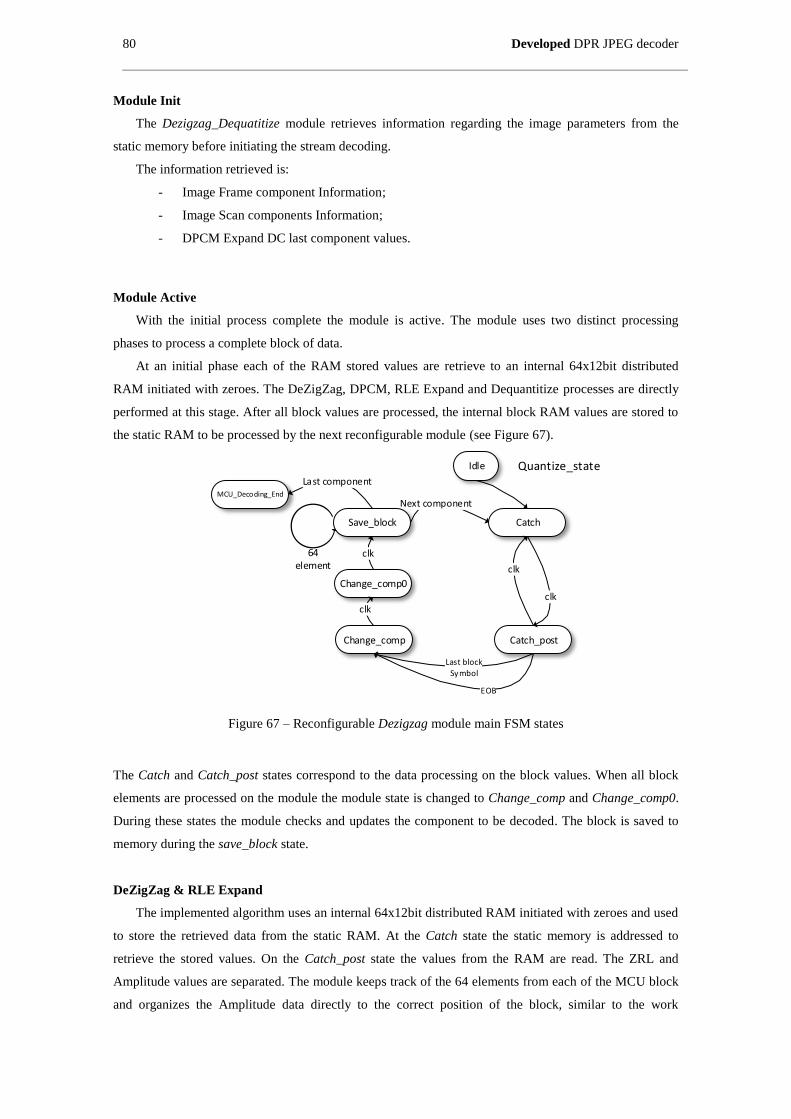
80 Developed DPR JPEG decoder
Module Init
The Dezigzag_Dequatitize module retrieves information regarding the image parameters from the
static memory before initiating the stream decoding.
The information retrieved is:
- Image Frame component Information;
- Image Scan components Information;
- DPCM Expand DC last component values.
Module Active
With the initial process complete the module is active. The module uses two distinct processing
phases to process a complete block of data.
At an initial phase each of the RAM stored values are retrieve to an internal 64x12bit distributed
RAM initiated with zeroes. The DeZigZag, DPCM, RLE Expand and Dequantitize processes are directly
performed at this stage. After all block values are processed, the internal block RAM values are stored to
the static RAM to be processed by the next reconfigurable module (see Figure 67).
Catch
Catch_post
Idle
Change_comp0
Change_comp
Last blockSymbol
EOB
Quantize_state
64 element
MCU_Decoding_End
Save_block
Figure 67 – Reconfigurable Dezigzag module main FSM states
The Catch and Catch_post states correspond to the data processing on the block values. When all block
elements are processed on the module the module state is changed to Change_comp and Change_comp0.
During these states the module checks and updates the component to be decoded. The block is saved to
memory during the save_block state.
DeZigZag & RLE Expand
The implemented algorithm uses an internal 64x12bit distributed RAM initiated with zeroes and used
to store the retrieved data from the static RAM. At the Catch state the static memory is addressed to
retrieve the stored values. On the Catch_post state the values from the RAM are read. The ZRL and
Amplitude values are separated. The module keeps track of the 64 elements from each of the MCU block
and organizes the Amplitude data directly to the correct position of the block, similar to the work
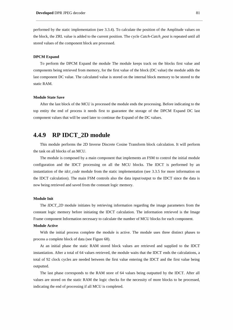
Developed DPR JPEG decoder 81
performed by the static implementation (see 3.3.4). To calculate the position of the Amplitude values on
the block, the ZRL value is added to the current position. The cycle Catch-Catch_post is repeated until all
stored values of the component block are processed.
DPCM Expand
To perform the DPCM Expand the module The module keeps track on the blocks first value and
components being retrieved from memory, for the first value of the block (DC value) the module adds the
last component DC value. The calculated value is stored on the internal block memory to be stored to the
static RAM.
Module State Save
After the last block of the MCU is processed the module ends the processing. Before indicating to the
top entity the end of process it needs first to guarantee the storage of the DPCM Expand DC last
component values that will be used later to continue the Expand of the DC values.
4.4.9 RP IDCT_2D module
This module performs the 2D Inverse Discrete Cosine Transform block calculation. It will perform
the task on all blocks of an MCU.
The module is composed by a main component that implements an FSM to control the initial module
configuration and the IDCT processing on all the MCU blocks. The IDCT is performed by an
instantiation of the idct_code module from the static implementation (see 3.3.5 for more information on
the IDCT calculation). The main FSM controls also the data input/output to the IDCT since the data is
now being retrieved and saved from the constant logic memory.
Module Init
The IDCT_2D module initiates by retrieving information regarding the image parameters from the
constant logic memory before initiating the IDCT calculation. The information retrieved is the Image
Frame component Information necessary to calculate the number of MCU blocks for each component.
Module Active
With the initial process complete the module is active. The module uses three distinct phases to
process a complete block of data (see Figure 68).
At an initial phase the static RAM stored block values are retrieved and supplied to the IDCT
instantiation. After a total of 64 values retrieved, the module waits that the IDCT ends the calculations, a
total of 92 clock cycles are needed between the first value entering the IDCT and the first value being
outputted.
The last phase corresponds to the RAM store of 64 values being outputted by the IDCT. After all
values are stored on the static RAM the logic checks for the necessity of more blocks to be processed,
indicating the end of processing if all MCU is completed.
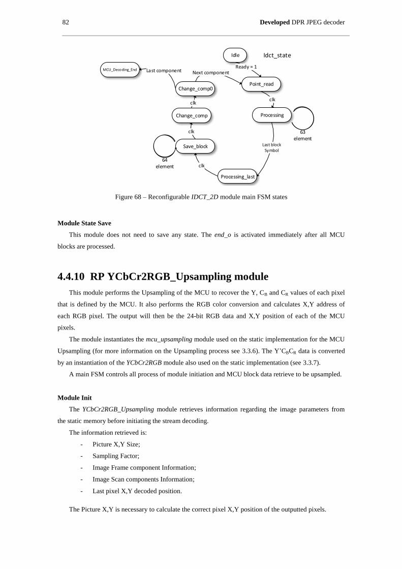
82 Developed DPR JPEG decoder
63 element
Point_read
Processing
Idle
Save_block
Processing_last
Idct_state
MCU_Decoding_End
64 element
Change_comp0
Change_comp
Figure 68 – Reconfigurable IDCT_2D module main FSM states
Module State Save
This module does not need to save any state. The end_o is activated immediately after all MCU
blocks are processed.
4.4.10 RP YCbCr2RGB_Upsampling module
This module performs the Upsampling of the MCU to recover the Y, CB and CR values of each pixel
that is defined by the MCU. It also performs the RGB color conversion and calculates X,Y address of
each RGB pixel. The output will then be the 24-bit RGB data and X,Y position of each of the MCU
pixels.
The module instantiates the mcu_upsampling module used on the static implementation for the MCU
Upsampling (for more information on the Upsampling process see 3.3.6). The Y’CBCR data is converted
by an instantiation of the YCbCr2RGB module also used on the static implementation (see 3.3.7).
A main FSM controls all process of module initiation and MCU block data retrieve to be upsampled.
Module Init
The YCbCr2RGB_Upsampling module retrieves information regarding the image parameters from
the static memory before initiating the stream decoding.
The information retrieved is:
- Picture X,Y Size;
- Sampling Factor;
- Image Frame component Information;
- Image Scan components Information;
- Last pixel X,Y decoded position.
The Picture X,Y is necessary to calculate the correct pixel X,Y position of the outputted pixels.
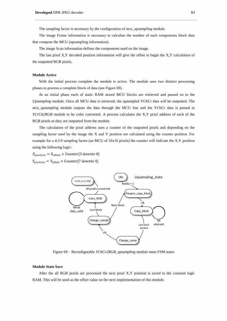
Developed DPR JPEG decoder 83
The sampling factor is necessary by the configuration of mcu_upsampling module.
The image Frame information is necessary to calculate the number of each components block data
that compose the MCU (upsampling information).
The image Scan information defines the components used on the image.
The last pixel X,Y decoded position information will give the offset to begin the X,Y calculation of
the outputted RGB pixels.
Module Active
With the initial process complete the module is active. The module uses two distinct processing
phases to process a complete block of data (see Figure 69).
At an initial phase each of static RAM stored MCU blocks are retrieved and passed on to the
Upsampling module. Once all MCU data is retrieved, the upsampled YCbCr data will be outputted. The
mcu_upsampling module outputs the data through the MCU line and the YCbCr data is passed to
YCrCb2RGB module to be color converted. A process calculates the X,Y pixel address of each of the
RGB pixels as they are outputted from the module.
The calculation of the pixel address uses a counter of the outputted pixels and depending on the
sampling factor used by the image the X and Y position are calculated using the counter position. For
example for a 4:2:0 sampling factor (an MCU of 16x16 pixels) the counter will indicate the X,Y position
using the following logic:
63 element
Prepare_copy_block
Copy_block
Idle
Change_comp0
Change_comp
Upsampling_stateFinish_conv_RGB
While data_valid
Conv_RGB
Figure 69 – Reconfigurable YCbCr2RGB_upsampling module main FSM states
Module State Save
After the all RGB pixels are processed the next pixel X,Y position is saved to the constant logic
RAM. This will be used as the offset value on the next implementation of this module.
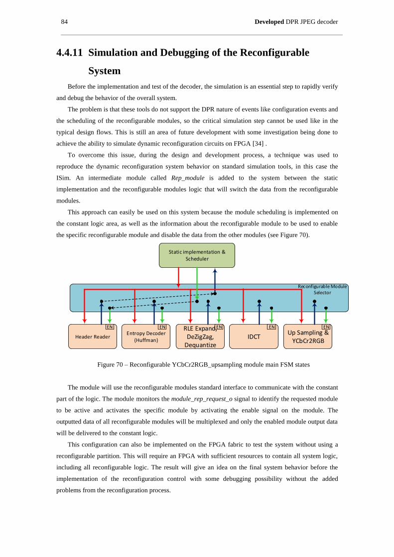
84 Developed DPR JPEG decoder
4.4.11 Simulation and Debugging of the Reconfigurable
System
Before the implementation and test of the decoder, the simulation is an essential step to rapidly verify
and debug the behavior of the overall system.
The problem is that these tools do not support the DPR nature of events like configuration events and
the scheduling of the reconfigurable modules, so the critical simulation step cannot be used like in the
typical design flows. This is still an area of future development with some investigation being done to
achieve the ability to simulate dynamic reconfiguration circuits on FPGA [34] .
To overcome this issue, during the design and development process, a technique was used to
reproduce the dynamic reconfiguration system behavior on standard simulation tools, in this case the
ISim. An intermediate module called Rep_module is added to the system between the static
implementation and the reconfigurable modules logic that will switch the data from the reconfigurable
modules.
This approach can easily be used on this system because the module scheduling is implemented on
the constant logic area, as well as the information about the reconfigurable module to be used to enable
the specific reconfigurable module and disable the data from the other modules (see Figure 70).
Entropy Decoder (Huffman)
RLE Expand, DeZigZag,
DequantizeIDCT
Up Sampling & YCbCr2RGB
Header Reader
Reconfigurable Module Selector
Static implementation & Scheduler
ENEN EN EN EN
Figure 70 – Reconfigurable YCbCr2RGB_upsampling module main FSM states
The module will use the reconfigurable modules standard interface to communicate with the constant
part of the logic. The module monitors the module_rep_request_o signal to identify the requested module
to be active and activates the specific module by activating the enable signal on the module. The
outputted data of all reconfigurable modules will be multiplexed and only the enabled module output data
will be delivered to the constant logic.
This configuration can also be implemented on the FPGA fabric to test the system without using a
reconfigurable partition. This will require an FPGA with sufficient resources to contain all system logic,
including all reconfigurable logic. The result will give an idea on the final system behavior before the
implementation of the reconfiguration control with some debugging possibility without the added
problems from the reconfiguration process.
Developed DPR JPEG decoder 85
This approach has some limitations, the most obvious is that is does not reproduce the system
behavior during reconfiguration. However, with cautioned design approach followed by the design
requirements referred in 2.2 it reduces the possibility to persist some design errors on the final
reconfigurable system. Another limitation is that the reconfiguration times are not taken into account so it
is not possible to retrieve a direct estimation of the overall system performance with the active
reconfiguration, this can be mitigated with careful study of the reconfiguration performance on the system
in hand and if necessary calculate an estimation of the final system performance (see Appendix C for an
example of system performance estimation). Using this approach also means that all system logic will be
simulated rather than the actual amount of logic used in the design making the simulation task more
processing demanding.
Debugging with ChipScope
Debugging of the system after implementation is essential in systems that for example interact with
external components that cannot be fully simulated. For those cases Xilinx gives the possibility to use
ChipScope, an In-System-Debugger that can be implemented and configured with the design. For designs
that use reconfigurable partitions the ChipScope cannot be used because it uses BUFG primitive. The
design rules do not allow using global clock resources such as BUFGs primitive on reconfigurable
partitions.
In this work, ChipScope was used and implemented as constant logic. To debug the reconfigurable
module a debug port dbg_data_32 was declared on the reconfigurable partition interface. The signals
from this port were routed inside the reconfigurable modules to the desired logic points giving an inside
“view” of the modules logic behavior. The same debug signals have different connections on each
module so monitored data depends on the implemented module.
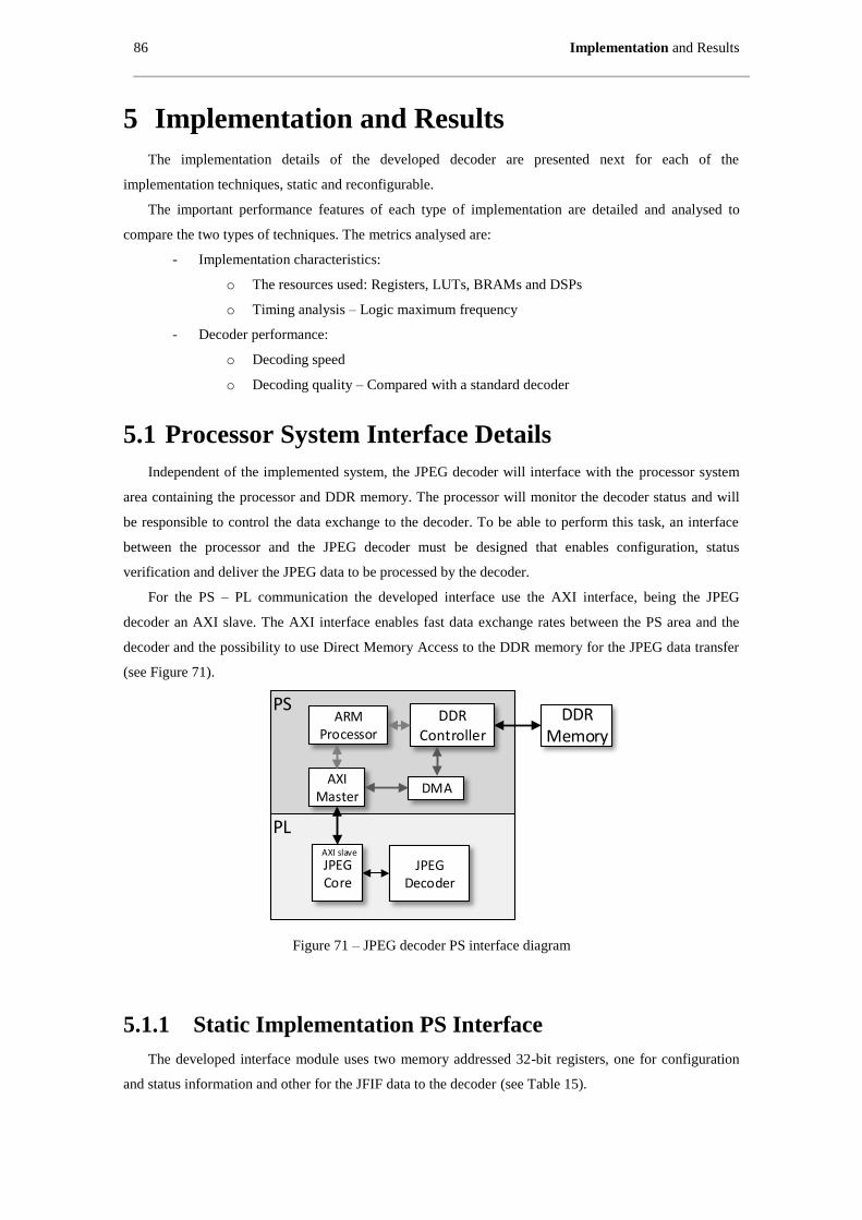
86 Implementation and Results
5 Implementation and Results
The implementation details of the developed decoder are presented next for each of the
implementation techniques, static and reconfigurable.
The important performance features of each type of implementation are detailed and analysed to
compare the two types of techniques. The metrics analysed are:
- Implementation characteristics:
o The resources used: Registers, LUTs, BRAMs and DSPs
o Timing analysis – Logic maximum frequency
- Decoder performance:
o Decoding speed
o Decoding quality – Compared with a standard decoder
5.1 Processor System Interface Details
Independent of the implemented system, the JPEG decoder will interface with the processor system
area containing the processor and DDR memory. The processor will monitor the decoder status and will
be responsible to control the data exchange to the decoder. To be able to perform this task, an interface
between the processor and the JPEG decoder must be designed that enables configuration, status
verification and deliver the JPEG data to be processed by the decoder.
For the PS – PL communication the developed interface use the AXI interface, being the JPEG
decoder an AXI slave. The AXI interface enables fast data exchange rates between the PS area and the
decoder and the possibility to use Direct Memory Access to the DDR memory for the JPEG data transfer
(see Figure 71).
PL
PS
AXI Master
DDR Memory
DDR Controller
JPEG Decoder
JPEG Core
ARM Processor
DMA
AXI slave
Figure 71 – JPEG decoder PS interface diagram
5.1.1 Static Implementation PS Interface
The developed interface module uses two memory addressed 32-bit registers, one for configuration
and status information and other for the JFIF data to the decoder (see Table 15).
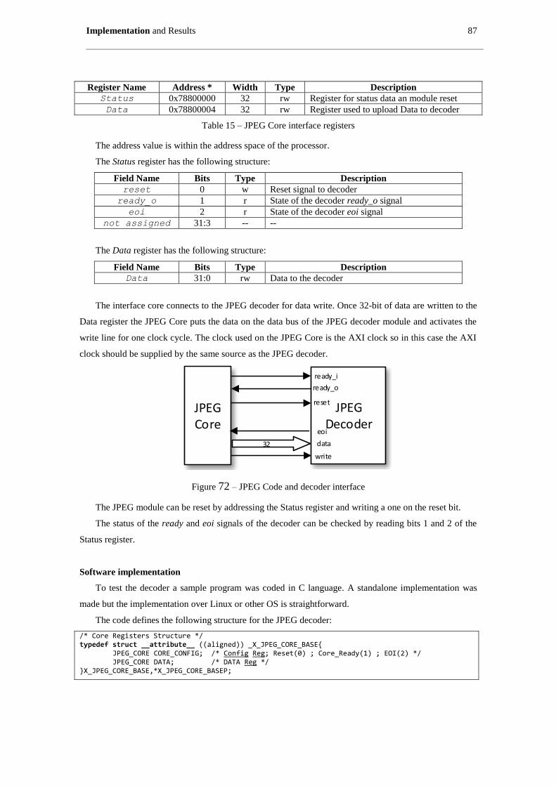
Implementation and Results 87
Register Name Address * Width Type Description
Status 0x78800000 32 rw Register for status data an module reset
Data 0x78800004 32 rw Register used to upload Data to decoder
Table 15 – JPEG Core interface registers
The address value is within the address space of the processor.
The Status register has the following structure:
Field Name Bits Type Description
reset 0 w Reset signal to decoder
ready_o 1 r State of the decoder ready_o signal
eoi 2 r State of the decoder eoi signal
not assigned 31:3 -- --
The Data register has the following structure:
Field Name Bits Type Description
Data 31:0 rw Data to the decoder
The interface core connects to the JPEG decoder for data write. Once 32-bit of data are written to the
Data register the JPEG Core puts the data on the data bus of the JPEG decoder module and activates the
write line for one clock cycle. The clock used on the JPEG Core is the AXI clock so in this case the AXI
clock should be supplied by the same source as the JPEG decoder.
JPEG Decoder
JPEG Core
ready_o
ready_i
reset
data
write
eoi
32
Figure 72 – JPEG Code and decoder interface
The JPEG module can be reset by addressing the Status register and writing a one on the reset bit.
The status of the ready and eoi signals of the decoder can be checked by reading bits 1 and 2 of the
Status register.
Software implementation
To test the decoder a sample program was coded in C language. A standalone implementation was
made but the implementation over Linux or other OS is straightforward.
The code defines the following structure for the JPEG decoder:
/* Core Registers Structure */ typedef struct __attribute__ ((aligned)) _X_JPEG_CORE_BASE{ JPEG_CORE CORE_CONFIG; /* Config Reg; Reset(0) ; Core_Ready(1) ; EOI(2) */ JPEG_CORE DATA; /* DATA Reg */ }X_JPEG_CORE_BASE,*X_JPEG_CORE_BASEP;
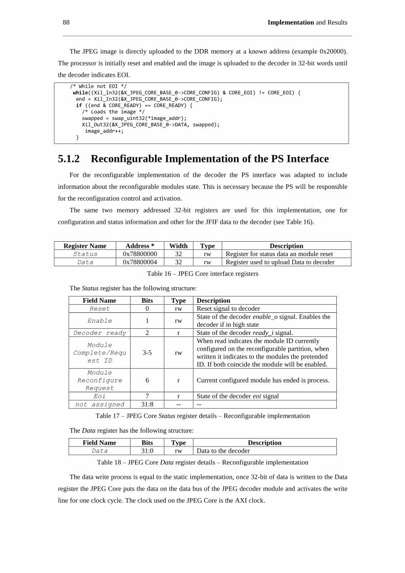
88 Implementation and Results
The JPEG image is directly uploaded to the DDR memory at a known address (example 0x20000).
The processor is initially reset and enabled and the image is uploaded to the decoder in 32-bit words until
the decoder indicates EOI.
/* While not EOI */ while((Xil_In32(&X_JPEG_CORE_BASE_0->CORE_CONFIG) & CORE_EOI) != CORE_EOI) { end = Xil_In32(&X_JPEG_CORE_BASE_0->CORE_CONFIG); if ((end & CORE_READY) == CORE_READY) { /* Loads the image */ swapped = swap_uint32(*image_addr); Xil_Out32(&X_JPEG_CORE_BASE_0->DATA, swapped); image_addr++; }
5.1.2 Reconfigurable Implementation of the PS Interface
For the reconfigurable implementation of the decoder the PS interface was adapted to include
information about the reconfigurable modules state. This is necessary because the PS will be responsible
for the reconfiguration control and activation.
The same two memory addressed 32-bit registers are used for this implementation, one for
configuration and status information and other for the JFIF data to the decoder (see Table 16).
Register Name Address * Width Type Description
Status 0x78800000 32 rw Register for status data an module reset
Data 0x78800004 32 rw Register used to upload Data to decoder
Table 16 – JPEG Core interface registers
The Status register has the following structure:
Field Name Bits Type Description
Reset 0 rw Reset signal to decoder
Enable 1 rw State of the decoder enable_o signal. Enables the
decoder if in high state
Decoder ready 2 r State of the decoder ready_i signal.
Module
Complete/Requ
est ID
3-5 rw
When read indicates the module ID currently
configured on the reconfigurable partition, when
written it indicates to the modules the pretended
ID. If both coincide the module will be enabled.
Module
Reconfigure
Request
6 r Current configured module has ended is process.
Eoi 7 r State of the decoder eoi signal
not assigned 31:8 -- --
Table 17 – JPEG Core Status register details – Reconfigurable implementation
The Data register has the following structure:
Field Name Bits Type Description
Data 31:0 rw Data to the decoder
Table 18 – JPEG Core Data register details – Reconfigurable implementation
The data write process is equal to the static implementation, once 32-bit of data is written to the Data
register the JPEG Core puts the data on the data bus of the JPEG decoder module and activates the write
line for one clock cycle. The clock used on the JPEG Core is the AXI clock.
Implementation and Results 89
JPEG Decoder
JPEG Core
ready_o
ready_i
reset
data
write
eoi
32
Module_end
3
3 Module_request
Module_complete
Figure 73 – JPEG Code and decoder interface – Reconfigurable implementation
Software implementation
As for the static implementation, to test the decoder a sample program coded in C language was used.
The code defines a similar register structure for the JPEG decoder:
/* Core Registers Structure */ typedef struct __attribute__ ((aligned)) _X_JPEG_CORE_BASE{ JPEG_CORE CORE_CONFIG; /* Config Reg Reset(0) R/W, Enable(1) R/W, Ready(2) R/W, Module_ID(3-5) R(request)/W(complete), module_request(6) R, EOI(2) R */ JPEG_CORE DATA; /* DATA Reg Data(0-31) R */ }X_JPEG_CORE_BASE,*X_JPEG_CORE_BASEP;
The JPEG image is directly uploaded to the DDR memory at a known address (example 0x20000).
For the reconfiguration the DMA is configured to send data to the PCAP with the address of the
bitstream files.
int XDcfg_TransferBitfile(XDcfg *Instance, u32 StartAddress, u32 WordLength) { int Status; volatile u32 IntrStsReg = 0; /* Clear DMA and PCAP Done Interrupts */ XDcfg_IntrClear(Instance, XDCFG_IXR_D_P_DONE_MASK); /* Transfer bitstream from DDR into fabric in non secure mode */ Status = XDcfg_Transfer(Instance, (u32 *) StartAddress, WordLength, (u32 *) XDCFG_DMA_INVALID_ADDRESS, 0, XDCFG_NON_SECURE_PCAP_WRITE); if (Status != XST_SUCCESS) return Status; /* Poll PCAP Done Interrupt */ while ((IntrStsReg & XDCFG_IXR_D_P_DONE_MASK) != XDCFG_IXR_D_P_DONE_MASK) IntrStsReg = XDcfg_IntrGetStatus(Instance); return XST_SUCCESS; }
The PS verifies that the correct module is configured, pulling the Module_Reconfigure_Request bit
and checking the Module_request_ID.
Core_Status = Xil_In32((unsigned int)&X_JPEG_CORE_BASE_0->CORE_CONFIG); if ((Core_Status & CORE_READY) == CORE_READY) { /* Loads the image */ swapped = swap_uint32(*image_addr); Xil_Out32((unsigned int)&X_JPEG_CORE_BASE_0->DATA, swapped); image_addr++; }
90 Implementation and Results
/* Verify if new module is necessary */ if ((Core_Status & WAITING_MOD) == WAITING_MOD) { /* New Reconfigurable Module Request */ switch (Core_Status & MODULE_ID) { /* Yes, verify the requested module ID */
…
The processor is initially reset and enabled and the image is uploaded to the decoder in 32-bit words
until the decoder indicates EOI.
5.2 Auxiliary modules Implementation
For the static implementation of the decoder, additional modules where introduced to obtain a
complete decoding system.
VGA Driver
The output of the decoder was connected to a VGA interface implemented on the PL. This interface
can connect to a VGA display and present to the user the decoded image. It will receive the decoded RGB
data values and display the decoded image on the VGA display.
The VGA module is based on standard VHDL code available (see Figure 74). It is composed by the
following components:
VGA_SYNC
This module controls the HW interface for the VGA monitor, generating the necessary
synchronization signals for an 800x600 image resolution. The pixel data is retrieved from a
video RAM. For the desired resolution the module must be clocked with a 50MHz clock;
READ_RAM
This module controls the video RAM. The video RAM is implemented using logic resources
of the FPGA, in this case block RAM (BRAM). For a full 800x600 resolution, the number of
resources needed overcome the available on the test system. To reduce the used resources
the resolution is limited to a maximum of 320x200. This module verifies that the correct
memory address is read from the video memory during the image scanning;
BLOCK_RAM
This represents the video memory module. As referred the used memory is block RAM.
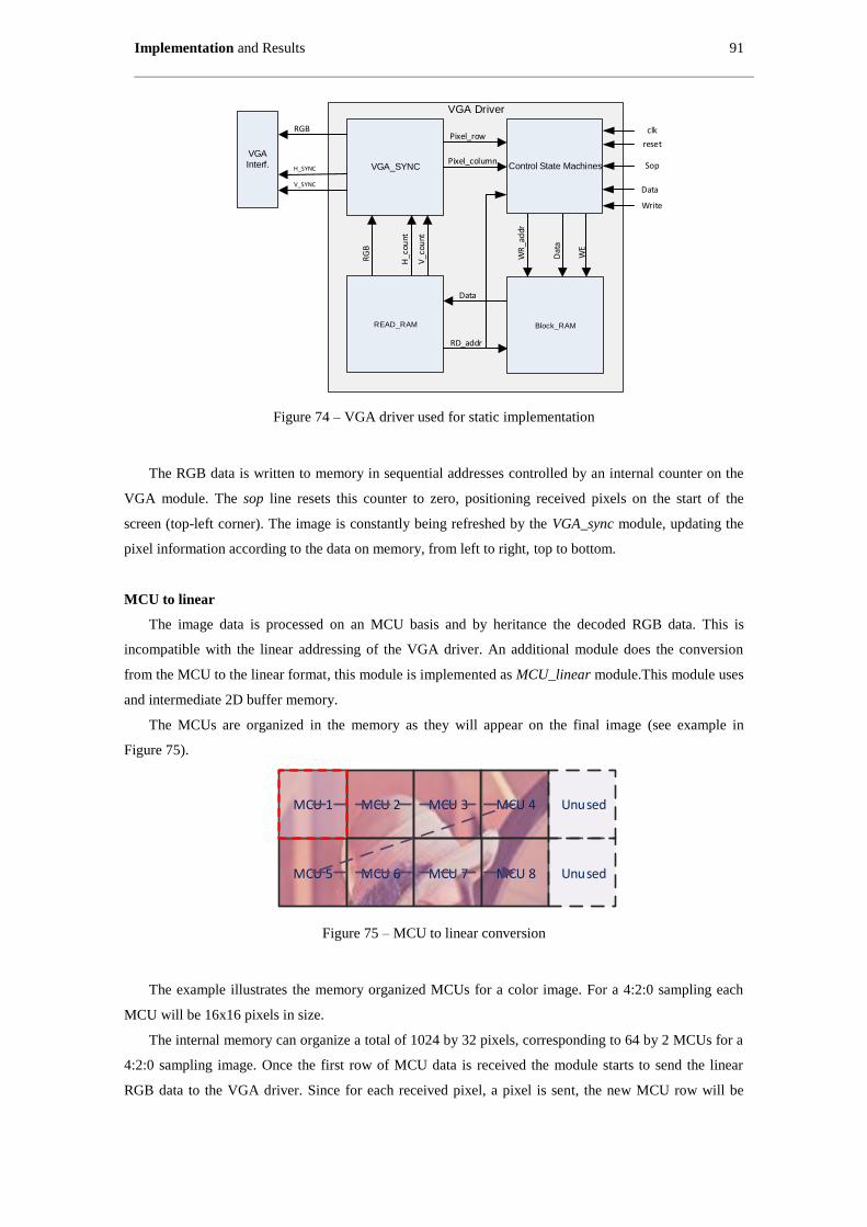
Implementation and Results 91
VGA Driver
VGA_SYNC
READ_RAM
VGAInterf.
H_c
ount
V_c
ount
RG
B
RD_addr
Data
Pixel_column
Pixel_rowRGB
H_SYNC
V_SYNC
Block_RAM
WR
_ad
dr
Dat
a
WE
Control State Machines
Write
Data
Sop
clk
reset
Figure 74 – VGA driver used for static implementation
The RGB data is written to memory in sequential addresses controlled by an internal counter on the
VGA module. The sop line resets this counter to zero, positioning received pixels on the start of the
screen (top-left corner). The image is constantly being refreshed by the VGA_sync module, updating the
pixel information according to the data on memory, from left to right, top to bottom.
MCU to linear
The image data is processed on an MCU basis and by heritance the decoded RGB data. This is
incompatible with the linear addressing of the VGA driver. An additional module does the conversion
from the MCU to the linear format, this module is implemented as MCU_linear module.This module uses
and intermediate 2D buffer memory.
The MCUs are organized in the memory as they will appear on the final image (see example in
Figure 75).
MCU 2 MCU 3 MCU 4
MCU 5 MCU 6 MCU 7 MCU 8
MCU 1 Unused
Unused
Figure 75 – MCU to linear conversion
The example illustrates the memory organized MCUs for a color image. For a 4:2:0 sampling each
MCU will be 16x16 pixels in size.
The internal memory can organize a total of 1024 by 32 pixels, corresponding to 64 by 2 MCUs for a
4:2:0 sampling image. Once the first row of MCU data is received the module starts to send the linear
RGB data to the VGA driver. Since for each received pixel, a pixel is sent, the new MCU row will be
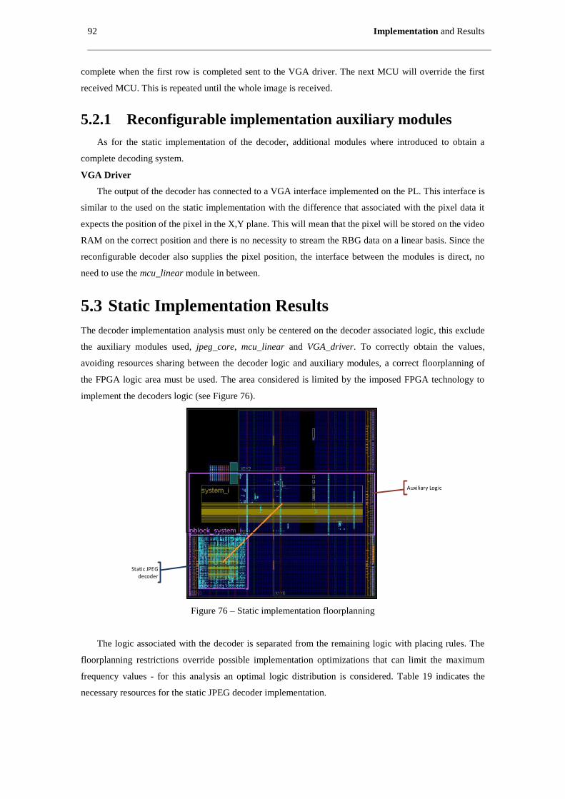
92 Implementation and Results
complete when the first row is completed sent to the VGA driver. The next MCU will override the first
received MCU. This is repeated until the whole image is received.
5.2.1 Reconfigurable implementation auxiliary modules
As for the static implementation of the decoder, additional modules where introduced to obtain a
complete decoding system.
VGA Driver
The output of the decoder has connected to a VGA interface implemented on the PL. This interface is
similar to the used on the static implementation with the difference that associated with the pixel data it
expects the position of the pixel in the X,Y plane. This will mean that the pixel will be stored on the video
RAM on the correct position and there is no necessity to stream the RBG data on a linear basis. Since the
reconfigurable decoder also supplies the pixel position, the interface between the modules is direct, no
need to use the mcu_linear module in between.
5.3 Static Implementation Results
The decoder implementation analysis must only be centered on the decoder associated logic, this exclude
the auxiliary modules used, jpeg_core, mcu_linear and VGA_driver. To correctly obtain the values,
avoiding resources sharing between the decoder logic and auxiliary modules, a correct floorplanning of
the FPGA logic area must be used. The area considered is limited by the imposed FPGA technology to
implement the decoders logic (see Figure 76).
Static JPEG decoder
Auxiliary Logic
Figure 76 – Static implementation floorplanning
The logic associated with the decoder is separated from the remaining logic with placing rules. The
floorplanning restrictions override possible implementation optimizations that can limit the maximum
frequency values - for this analysis an optimal logic distribution is considered. Table 19 indicates the
necessary resources for the static JPEG decoder implementation.
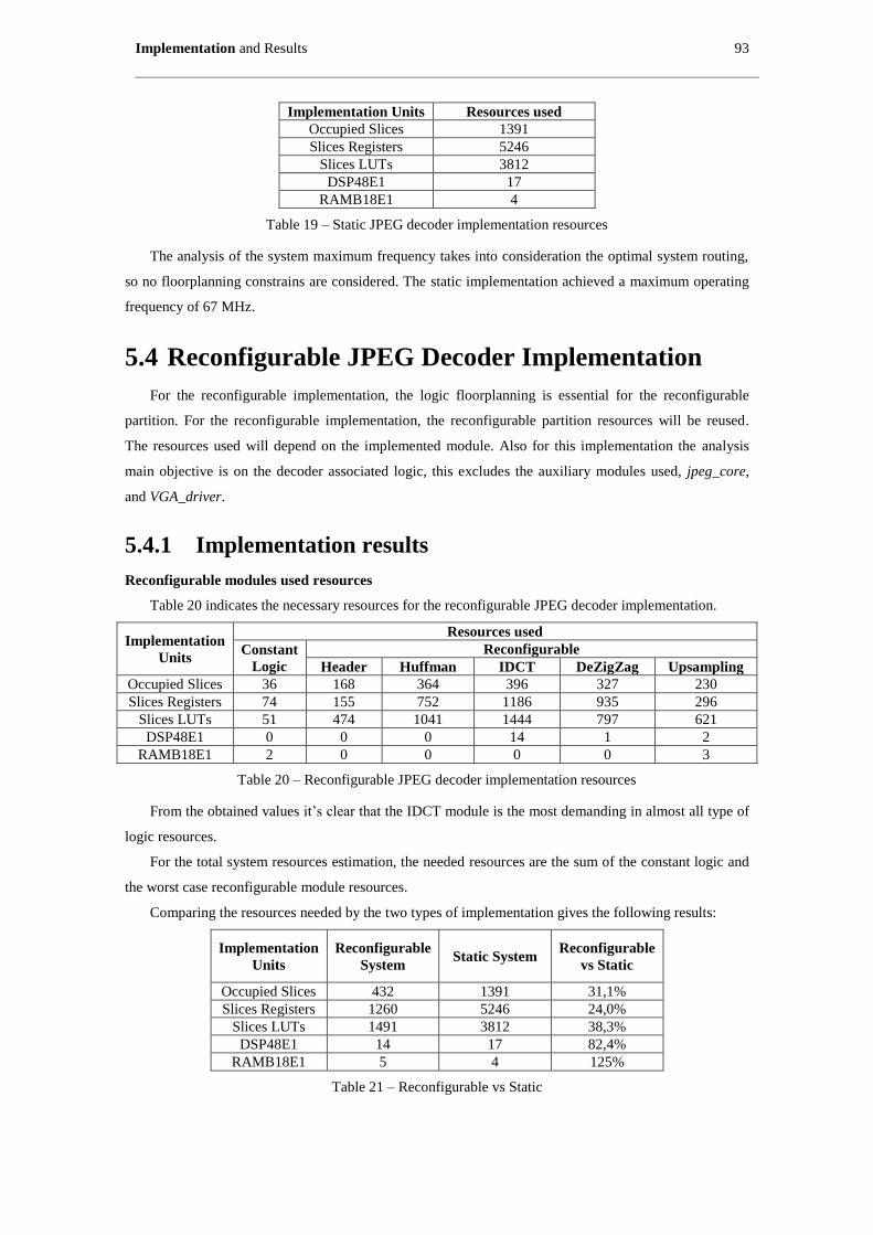
Implementation and Results 93
Implementation Units Resources used
Occupied Slices 1391
Slices Registers 5246
Slices LUTs 3812
DSP48E1 17
RAMB18E1 4
Table 19 – Static JPEG decoder implementation resources
The analysis of the system maximum frequency takes into consideration the optimal system routing,
so no floorplanning constrains are considered. The static implementation achieved a maximum operating
frequency of 67 MHz.
5.4 Reconfigurable JPEG Decoder Implementation
For the reconfigurable implementation, the logic floorplanning is essential for the reconfigurable
partition. For the reconfigurable implementation, the reconfigurable partition resources will be reused.
The resources used will depend on the implemented module. Also for this implementation the analysis
main objective is on the decoder associated logic, this excludes the auxiliary modules used, jpeg_core,
and VGA_driver.
5.4.1 Implementation results
Reconfigurable modules used resources
Table 20 indicates the necessary resources for the reconfigurable JPEG decoder implementation.
Implementation
Units
Resources used
Constant
Logic
Reconfigurable
Header Huffman IDCT DeZigZag Upsampling
Occupied Slices 36 168 364 396 327 230
Slices Registers 74 155 752 1186 935 296
Slices LUTs 51 474 1041 1444 797 621
DSP48E1 0 0 0 14 1 2
RAMB18E1 2 0 0 0 0 3
Table 20 – Reconfigurable JPEG decoder implementation resources
From the obtained values it’s clear that the IDCT module is the most demanding in almost all type of
logic resources.
For the total system resources estimation, the needed resources are the sum of the constant logic and
the worst case reconfigurable module resources.
Comparing the resources needed by the two types of implementation gives the following results:
Implementation
Units
Reconfigurable
System Static System
Reconfigurable
vs Static
Occupied Slices 432 1391 31,1%
Slices Registers 1260 5246 24,0%
Slices LUTs 1491 3812 38,3%
DSP48E1 14 17 82,4%
RAMB18E1 5 4 125%
Table 21 – Reconfigurable vs Static
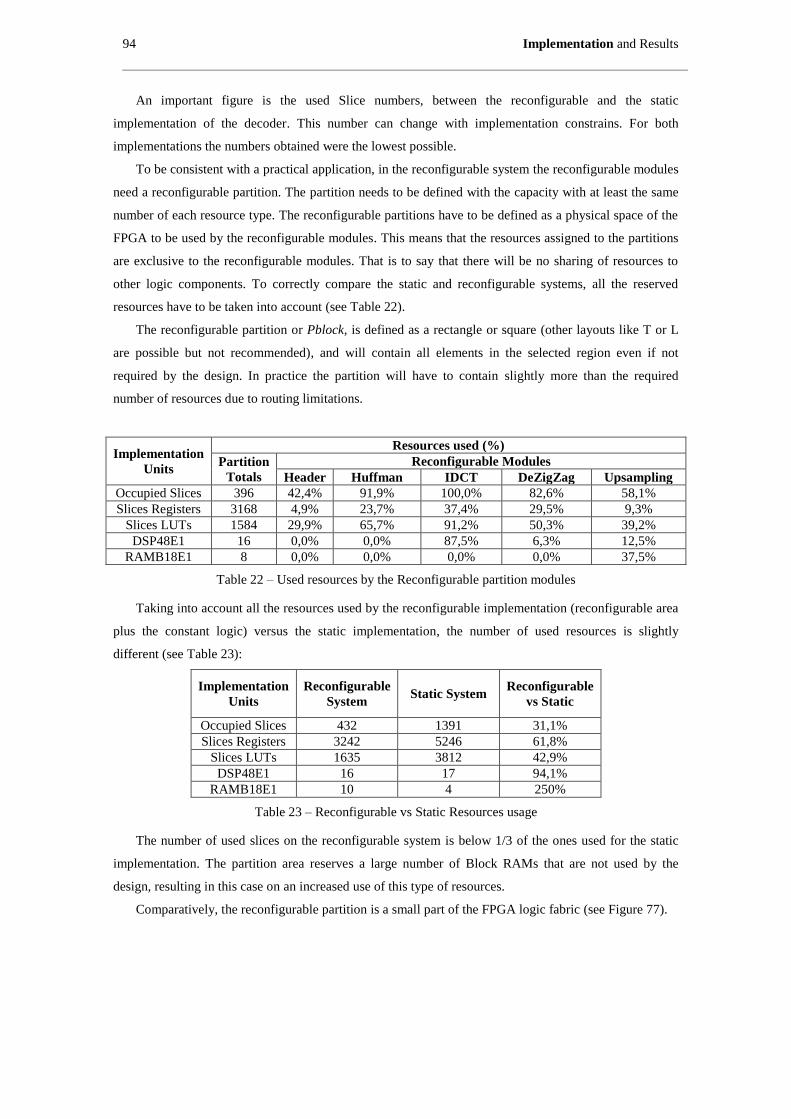
94 Implementation and Results
An important figure is the used Slice numbers, between the reconfigurable and the static
implementation of the decoder. This number can change with implementation constrains. For both
implementations the numbers obtained were the lowest possible.
To be consistent with a practical application, in the reconfigurable system the reconfigurable modules
need a reconfigurable partition. The partition needs to be defined with the capacity with at least the same
number of each resource type. The reconfigurable partitions have to be defined as a physical space of the
FPGA to be used by the reconfigurable modules. This means that the resources assigned to the partitions
are exclusive to the reconfigurable modules. That is to say that there will be no sharing of resources to
other logic components. To correctly compare the static and reconfigurable systems, all the reserved
resources have to be taken into account (see Table 22).
The reconfigurable partition or Pblock, is defined as a rectangle or square (other layouts like T or L
are possible but not recommended), and will contain all elements in the selected region even if not
required by the design. In practice the partition will have to contain slightly more than the required
number of resources due to routing limitations.
Implementation
Units
Resources used (%)
Partition
Totals
Reconfigurable Modules
Header Huffman IDCT DeZigZag Upsampling
Occupied Slices 396 42,4% 91,9% 100,0% 82,6% 58,1%
Slices Registers 3168 4,9% 23,7% 37,4% 29,5% 9,3%
Slices LUTs 1584 29,9% 65,7% 91,2% 50,3% 39,2%
DSP48E1 16 0,0% 0,0% 87,5% 6,3% 12,5%
RAMB18E1 8 0,0% 0,0% 0,0% 0,0% 37,5%
Table 22 – Used resources by the Reconfigurable partition modules
Taking into account all the resources used by the reconfigurable implementation (reconfigurable area
plus the constant logic) versus the static implementation, the number of used resources is slightly
different (see Table 23):
Implementation
Units
Reconfigurable
System Static System
Reconfigurable
vs Static
Occupied Slices 432 1391 31,1%
Slices Registers 3242 5246 61,8%
Slices LUTs 1635 3812 42,9%
DSP48E1 16 17 94,1%
RAMB18E1 10 4 250%
Table 23 – Reconfigurable vs Static Resources usage
The number of used slices on the reconfigurable system is below 1/3 of the ones used for the static
implementation. The partition area reserves a large number of Block RAMs that are not used by the
design, resulting in this case on an increased use of this type of resources.
Comparatively, the reconfigurable partition is a small part of the FPGA logic fabric (see Figure 77).
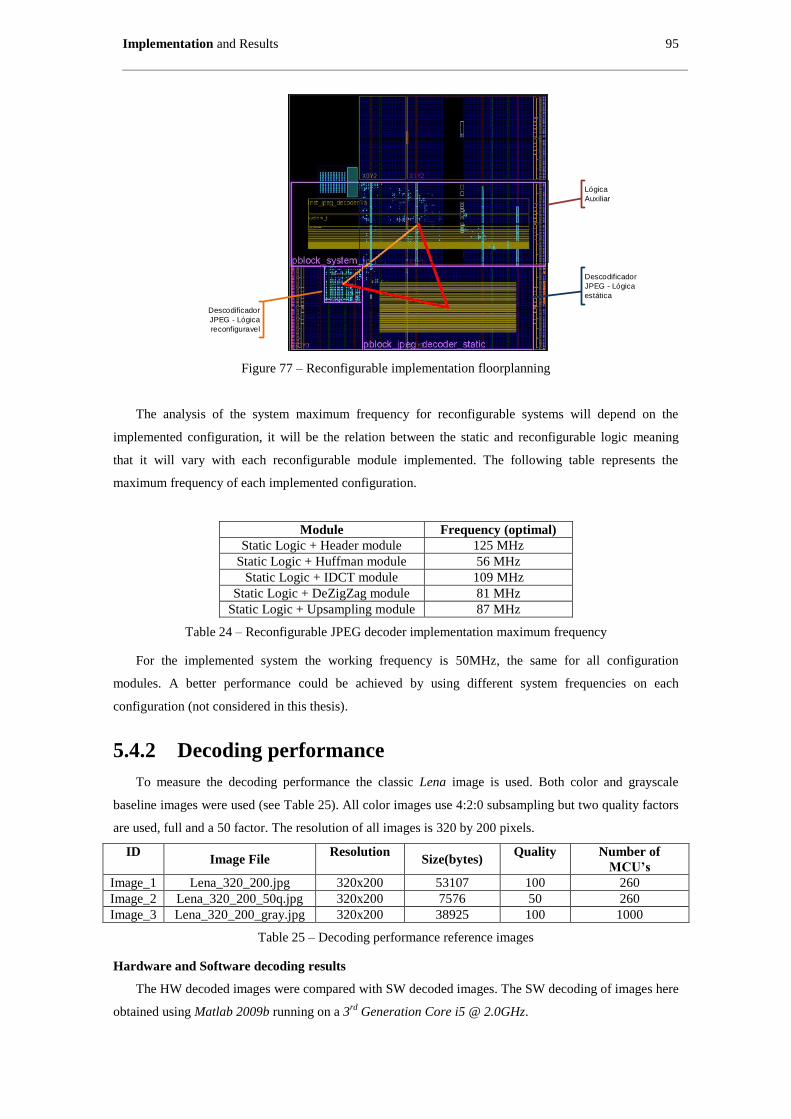
Implementation and Results 95
Lógica
Auxiliar
Descodificador
JPEG - Lógica
estática
Descodificador
JPEG - Lógica
reconfiguravel
Figure 77 – Reconfigurable implementation floorplanning
The analysis of the system maximum frequency for reconfigurable systems will depend on the
implemented configuration, it will be the relation between the static and reconfigurable logic meaning
that it will vary with each reconfigurable module implemented. The following table represents the
maximum frequency of each implemented configuration.
Module Frequency (optimal)
Static Logic + Header module 125 MHz
Static Logic + Huffman module 56 MHz
Static Logic + IDCT module 109 MHz
Static Logic + DeZigZag module 81 MHz
Static Logic + Upsampling module 87 MHz
Table 24 – Reconfigurable JPEG decoder implementation maximum frequency
For the implemented system the working frequency is 50MHz, the same for all configuration
modules. A better performance could be achieved by using different system frequencies on each
configuration (not considered in this thesis).
5.4.2 Decoding performance
To measure the decoding performance the classic Lena image is used. Both color and grayscale
baseline images were used (see Table 25). All color images use 4:2:0 subsampling but two quality factors
are used, full and a 50 factor. The resolution of all images is 320 by 200 pixels.
ID Image File
Resolution Size(bytes)
Quality Number of
MCU’s
Image_1 Lena_320_200.jpg 320x200 53107 100 260
Image_2 Lena_320_200_50q.jpg 320x200 7576 50 260
Image_3 Lena_320_200_gray.jpg 320x200 38925 100 1000
Table 25 – Decoding performance reference images
Hardware and Software decoding results
The HW decoded images were compared with SW decoded images. The SW decoding of images here
obtained using Matlab 2009b running on a 3rd
Generation Core i5 @ 2.0GHz.
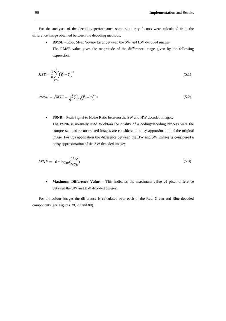
96 Implementation and Results
For the analyses of the decoding performance some similarity factors were calculated from the
difference image obtained between the decoding methods:
RMSE – Root Mean Square Error between the SW and HW decoded images.
The RMSE value gives the magnitude of the difference image given by the following
expression;
�
∑( ̂ )
(5.1)
√ √
∑ ( ̂ )
= (5.2)
PSNR – Peak Signal to Noise Ratio between the SW and HW decoded images.
The PSNR is normally used to obtain the quality of a coding/decoding process were the
compressed and reconstructed images are considered a noisy approximation of the original
image. For this application the difference between the HW and SW images is considered a
noisy approximation of the SW decoded image;
�
) (5.3)
Maximum Difference Value – This indicates the maximum value of pixel difference
between the SW and HW decoded images.
For the colour images the difference is calculated over each of the Red, Green and Blue decoded
components (see Figures 78, 79 and 80).
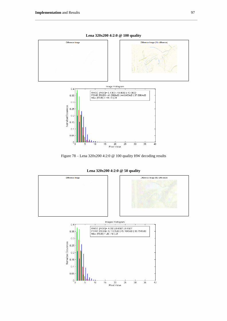
Implementation and Results 97
Lena 320x200 4:2:0 @ 100 quality
Figure 78 – Lena 320x200 4:2:0 @ 100 quality HW decoding results
Lena 320x200 4:2:0 @ 50 quality
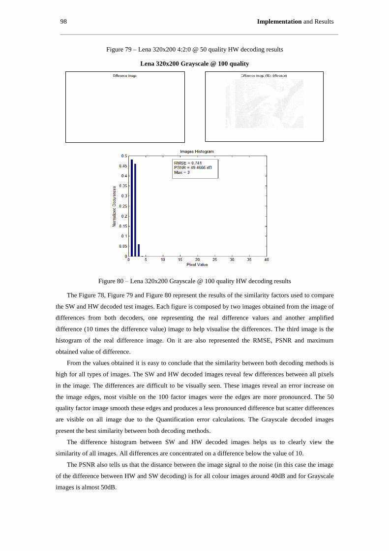
98 Implementation and Results
Figure 79 – Lena 320x200 4:2:0 @ 50 quality HW decoding results
Lena 320x200 Grayscale @ 100 quality
Figure 80 – Lena 320x200 Grayscale @ 100 quality HW decoding results
The Figure 78, Figure 79 and Figure 80 represent the results of the similarity factors used to compare
the SW and HW decoded test images. Each figure is composed by two images obtained from the image of
differences from both decoders, one representing the real difference values and another amplified
difference (10 times the difference value) image to help visualise the differences. The third image is the
histogram of the real difference image. On it are also represented the RMSE, PSNR and maximum
obtained value of difference.
From the values obtained it is easy to conclude that the similarity between both decoding methods is
high for all types of images. The SW and HW decoded images reveal few differences between all pixels
in the image. The differences are difficult to be visually seen. These images reveal an error increase on
the image edges, most visible on the 100 factor images were the edges are more pronounced. The 50
quality factor image smooth these edges and produces a less pronounced difference but scatter differences
are visible on all image due to the Quantification error calculations. The Grayscale decoded images
present the best similarity between both decoding methods.
The difference histogram between SW and HW decoded images helps us to clearly view the
similarity of all images. All differences are concentrated on a difference below the value of 10.
The PSNR also tells us that the distance between the image signal to the noise (in this case the image
of the difference between HW and SW decoding) is for all colour images around 40dB and for Grayscale
images is almost 50dB.
Implementation and Results 99
Module Reconfiguration time
An important information about the reconfigurable implementation is the reconfiguration time of the
decoder modules. The time will vary with the size of the bitstream files, technology, and implementation
consideration (e.g. use of DMA for the reconfiguration) (see Table 26).
Bitstream
applied Size(bytes)
Time for
configuration(us) Throughput(Mbps)
Complete 4045564 31106 1040,5
Partial 218000 1679 1038,7
Table 26 – System Reconfiguration time
The values were obtained using the PCAP interface and the DMA for the data transfer. The partial
reconfiguration time are the same for all reconfigurable modules (they have all the same bitstream size).
Additionally, the Bitstream files for reconfiguration are striped from all header information, normally
called bitstream bin files. Xilinx provides tools to directly obtain the bin files from the bitfiles as follows:
exec promgen –b –w –p bin –data_width 32 –u 0 <bit_file.bit> -o <bin_file.bin>
Decoding time
The decoding time of the test images was obtained for both implementations. The Matlab software
decoding time was also obtained using a 3rd
Generation Core i5 @ 2.0GHz processor. The software
decoding times were obtained using a software function with a variable resolution. The decoding value
was obtained using the mean value of 100 decoding interactions.
Tables 27, 28 and 29 summarizes the obtained decoding times for both implementations on the test
image.
Lena image (320x200 4:2:0 @ 100 quality factor – 260 MCU’s)
Implementation Time to decode(ms) Images per sec.
Static 17,074 58,56
Reconfigurable 1777 0,5627
SW Decoding
Matlab (Core i5 PC) 4,1 243
Table 27 – Decoding times for Lena image 320x200 4:2:0 @ 100 quality factor
Lena image (320x200 4:2:0 @ 50 quality factor – 260 MCU’s)
Implementation Time to decode(ms) Images per sec.
Static 5,95 168,1
Reconfigurable 1761 0,5678
SW Decoding
Matlab (Core i5 PC) 2,8 357
Table 28 – Decoding times for Lena image 320x200 4:2:0 @ 50 quality factor
Lena image (320x200 Grayscale @ 100 quality factor – 1000 MCU’s)
Implementation Time to decode(ms) Images per sec.
Static 12,035 83,1
Reconfigurable 6742 0,148
SW Decoding
Matlab (Core i5 PC) 2,3 357
Table 29 – Decoding times for Lena image 320x200 Grayscale @ 100 quality factor
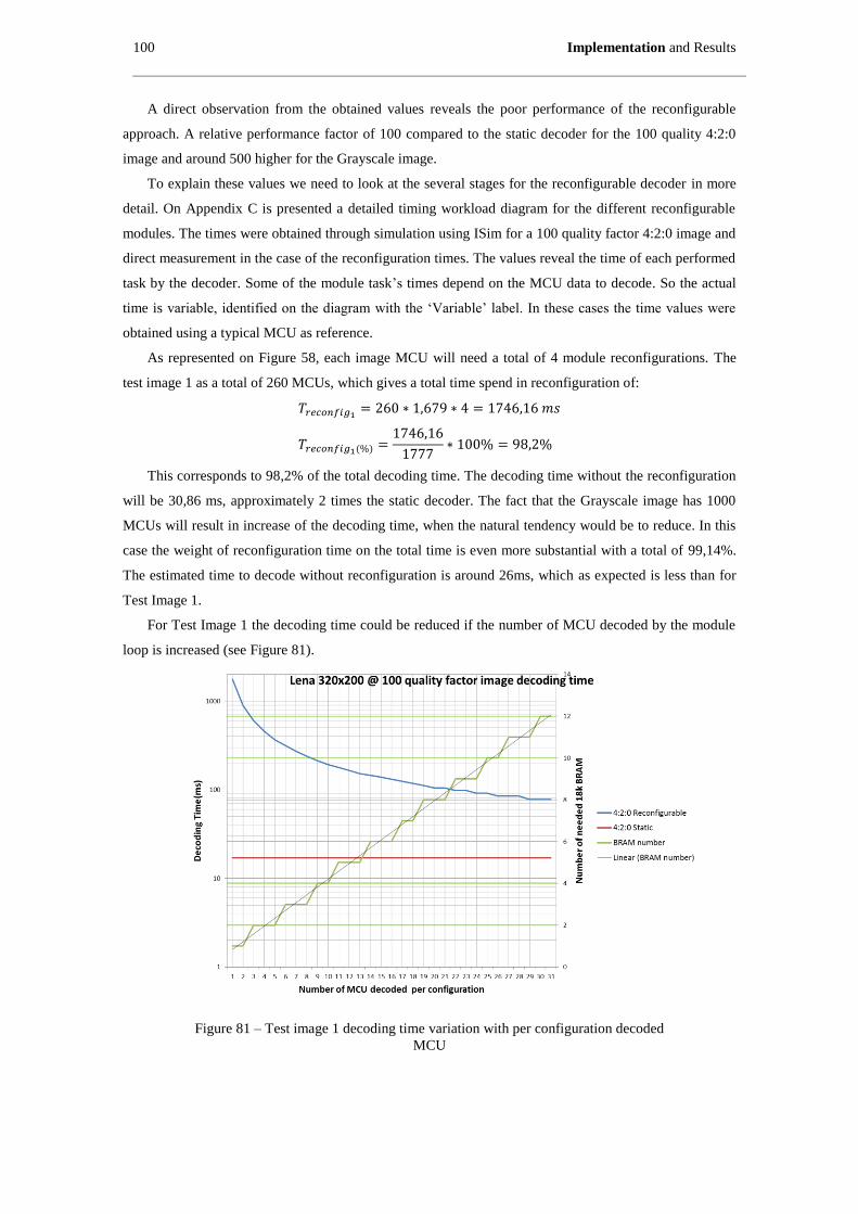
100 Implementation and Results
A direct observation from the obtained values reveals the poor performance of the reconfigurable
approach. A relative performance factor of 100 compared to the static decoder for the 100 quality 4:2:0
image and around 500 higher for the Grayscale image.
To explain these values we need to look at the several stages for the reconfigurable decoder in more
detail. On Appendix C is presented a detailed timing workload diagram for the different reconfigurable
modules. The times were obtained through simulation using ISim for a 100 quality factor 4:2:0 image and
direct measurement in the case of the reconfiguration times. The values reveal the time of each performed
task by the decoder. Some of the module task’s times depend on the MCU data to decode. So the actual
time is variable, identified on the diagram with the ‘Variable’ label. In these cases the time values were
obtained using a typical MCU as reference.
As represented on Figure 58, each image MCU will need a total of 4 module reconfigurations. The
test image 1 as a total of 260 MCUs, which gives a total time spend in reconfiguration of:
)
This corresponds to 98,2% of the total decoding time. The decoding time without the reconfiguration
will be 30,86 ms, approximately 2 times the static decoder. The fact that the Grayscale image has 1000
MCUs will result in increase of the decoding time, when the natural tendency would be to reduce. In this
case the weight of reconfiguration time on the total time is even more substantial with a total of 99,14%.
The estimated time to decode without reconfiguration is around 26ms, which as expected is less than for
Test Image 1.
For Test Image 1 the decoding time could be reduced if the number of MCU decoded by the module
loop is increased (see Figure 81).
Figure 81 – Test image 1 decoding time variation with per configuration decoded
MCU
Conclusions and future work 101
6 Conclusions and future work
The reconfigurability of the FPGA logic takes a new step forward when applied together with the
possibility to partially reconfigure the logic fabric. The logic can now be seen as a working platform that
can be adapted in a dynamic manner, freeing the technology resource limits and perform complicated
algorithms with extreme flexibility seen in the past as exclusively to software approaches. The DPR
opens new possibilities but there are still many limiting factors for this technology, mainly its intimate
relation with the physicality of the FPGA and for each vendor.
The DPR is also largely dependent on a processing unit for the reconfiguration control. This can be
overcome with current technology but greater benefits are obtained using a hybrid solution between the
software approach and the hardware, this is the main advantage of the new SoC systems like the one used
on this work.
The implementation results of the JPEG decoder implemented in this work demonstrates that the
DPR can address problems of resource limitation but this come with a cost. The adaptation of a system to
this approach requires an intense study and a great number of development hours. The approach used is
very severe on the overall decoder performance due to the intense reconfiguration work necessary to
perform the decoding algorithm. Simple changes to the used approach can improve dramatically the
performance of the system, without compromising the innumerous advantages that the approach offers.
One proposal of improvement is to increase the number of image MCU that can be decoded on each
module reconfiguration loop. Using the Block RAMs that became reserved by the reconfigurable partition
and use it to store the intermediate MCU values processed by each module, the number of
reconfigurations can be decreased without adding additional resources (see Figure 81).
Using for instance the reconfigurable partition reserved number of Block RAMs (6) the estimated
decoding time for the Test Image 1 with a total of 260 MCUs is around 131ms, similar to 7 times the
static implementation.
With respect to the used resources of the FPGA, as expected the reconfigurable approach gets the
best results. The slice resources used where reduced to almost half of the static implementation. This
result means that the reconfigurable decoder can be used on low resources FPGA where the static
implementation cannot be used.
Also the results from the implementation of the reconfigurable decoder demonstrated the possibility
to run the reconfigurable modules at different clock rates, this allied to the use of pipeline design in
critical components like the IDCT could improve the overall performance of the decoding process. The
reconfigurable approach also gains from the fact that with less logic resources used the overall placement
can be optimized, resulting in better performance and an increased usage of the granularity of the FPGA.
A DPR approach can also be used in implementations that consider the reconfiguration of a complete
decoder. Whole reconfigured decoders would perform equal or even better when compared with the static
implementation since no reconfiguration time would be added to the process (excluding the initial
reconfiguration time).
102 Conclusions and future work
One use of this approach could be the development of a JPEG decoder fully compliant with the
specification processes, as referenced in Table 1. A static implementation of a fully compliant decoder
could mean the use of innumerous resources due to the fact that it should be designed to process different
approaches to intensive processing tasks like Huffman coding or Arithmetic, DCT-process or Predictive.
In the static decoder the logic to cope with such different coding processes would mean that innumerous
resources would just be reserved to the event that images with different coding process needed to be
decoded. A DPR decoder would implement the specific logic to decode each image by initially reading
the JFIF data and implementing the specific decoder to process the data stream. The logic to be
implemented would only be the necessary to decode each of the coding processes defined on the JPEG
standard, resulting in a resource optimization and eventually better performance by the optimal placement
of logic.
One of the limitations of the DPR based-solution is the close dependency of a processing unit to
control the reconfiguration process. The use of a fully autonomous DPR decoder would include the
control of an ICAP component for the reconfiguration and the access to a memory resource like the DDR
memory or and SD Card for the bitstreams data storage. The reconfiguration logic would verify the need
for reconfiguration, access the memory resource that holds the bitstream data for the reconfigurable
modules and implement then into the fabric using the ICAP component.

Appendix 103
Appendix
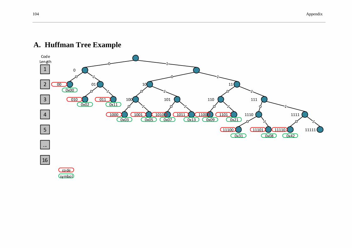
104 Appendix
A. Huffman Tree Example
00
0
01
010 011
10 11
110 111100 101
1000 1001 1010 1011 1100 1111
11110 11111
11101101
11100 11101
Code Length
16
5
4
3
2
1
...
0x00
0x02 0x11
0x03 0x05 0x07 0x13 0x09 0x21
0x31 0x08 0x42
code
symbol
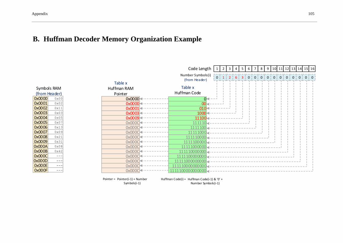
Appendix 105
B. Huffman Decoder Memory Organization Example
Code Length 1 2 3 4 5 6 7 8 9 10 11 12 13 14 15 16
000
0 1 2 6 3 0 0 0 0 0 0 0 0 0 0 0Number Symbols(i)
(from Header)
Table xHuffman Code
010
11100111110
111110011111000
1111100001111100000
11111000000111110000000
111110000000011111000000000
1111100000000001111100000000000
1000
Huffman Code(i) =
0x00000x0000
Table xHuffman RAM
Pointer
0x0001
0x00090x000C0x000C0x000C0x000C0x000C0x000C0x000C0x000C0x000C0x000C0x000C
0x0003
0x000C
Huffman Code(i-1) & ‘0’ + Number Symbols(i-1)
Pointer = Pointer(i-1) + Number Symbols(i-1)
0x00000x0001
Symbols RAM(from Header)
0x0002
0x00040x000C0x00060x00070x00080x00090x000A0x000B0x000C0x000D0x000E0x000F
0x0003
0x0005
0x00
0x02
0x11
0x05
0x000C
0x13
0x09
0x21
0x31
0x08
0x42
---
---
---
---
0x03
0x07
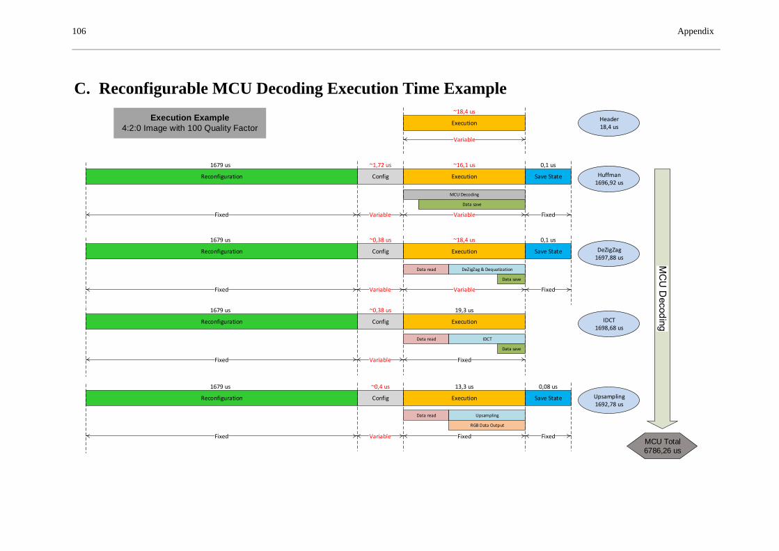
106 Appendix
C. Reconfigurable MCU Decoding Execution Time Example
ExecutionConfigReconfiguration Save State
1679 us ~1,72 us ~16,1 us 0,1 us
MCU Decoding
Data save
Huffman1696,92 us
Fixed Variable Variable Fixed
Execution
~18,4 usHeader18,4 us
Variable
ExecutionConfigReconfiguration Save State
1679 us ~0,38 us ~18,4 us 0,1 us
Data read DeZigZag & Dequatization
DeZigZag1697,88 us
Fixed Variable Variable Fixed
ExecutionConfigReconfiguration
1679 us ~0,38 us 19,3 us
IDCT1698,68 us
Fixed Variable Fixed
ExecutionConfigReconfiguration Save State
1679 us ~0,4 us 13,3 us 0,08 us
Upsampling1692,78 us
Fixed Variable Fixed Fixed
Data save
Data read IDCT
Data save
Data read Upsampling
RGB Data Output
MCU Total
6786,26 us
Execution Example
4:2:0 Image with 100 Quality Factor
Bibliography 107
Bibliography
[1] I. Kuon e J. Rose, “Measuring the gap between FPGAs and ASICs,” IEEE Transactions on
Computer-Aided Design of Integrated Circuits and Systems, vol. 26, pp. 203-215, 2007.
[2] Xilinx, “Zynq-7000 All Programmable SoC Overview DS190 (v1.7)", 2014.
[3] Xilinx, "Zynq-7000 All Programmable SoC - Technical Reference Manual UG585 (v1.9.1)", 2014.
[4] AVNET, “ZedBoard - Zynq™ Evaluation and Development Hardware User's Guide - ver.1.6,”
AVNET, 2012.
[5] G. Estrin, Organization of Computer Systems - The Fixed plus Variable Structure Computer, Los
Angeles, California: University of California, 1960.
[6] B. Zeidman, “All about FPGAs,” EETimes, 2006. [Online]. Available:
http://www.eetimes.com/document.asp?doc_id=1274496. [Acedido em Feb 2015].
[7] WikiBooks, “Programmable Logic/FPGAs,” [Online]. Available:
http://en.wikibooks.org/wiki/Programmable_Logic/FPGAs. [Acedido em January 2015].
[8] J. Kouloheris e A. El Gamal, “PLA-based FPGA Area Versus Cell C+ Granularity,” Proceedings of
the IEEE 1992 Custom Integrated Circuits Conference, pp. 4.3.1-4.3.4, May 1992.
[9] J. Rose, R. Francis, D. Lewis e P. Chow, “Architecture of field-programmable gate arrays: the effect
of logic block functionality on area efficiency,” IEEE Journal of Solid-State Circuits, vol. 25, pp.
1217-1225, Oct. 1990.
[10] S. Singh, J. Rose, P. Chow e D. Lewis, “The effect of logic block architecture on FPGA
performance,” IEEE Journal of Solid-State Circuits, Vols. %1 de %227, no. 3, pp. 281-287, Mar.
1992.
[11] S. Singh, “The effect of logic block architecture on FPGA performance,” M.A.Sc. thesis, Univ.
Toronto, 1991.
[12] Xilinx, “UG702 - Partial Reconfiguration User Guide (v14.5),” Xilinx, 2013.
[13] Xilinx, "Difference-Based Partial Reconfiguration - XAPP290", 2007.
[14] Y. Hori, H. Yokoyama, H. Sakane e K. Toda, “"A Secure Digital Content Delivery System Based on
Partially Reconfigurable Hardware",” International Conference on Field-Programmable
Technology, 2007. ICFPT 2007, pp. 253-256, Dec 2007.
[15] Y. Hori, H. Sakane e K. Toda, “A study of the effectiveness of dynamic partial reconfiguration for
size and power reduction,” IEICE Tech. Rep , vol. 107, pp. 31-36, Jan 2008.
[16] S. Liu, R. N. Pittman e A. Forin, “Energy Reduction with Run-Time Partial Reconfiguration,”
Microsoft Corporation, 2009.
[17] C. Claus, J. Zeppenfeld, F. Muller e W. Stechele, “Using Partial-Run-Time Reconfigurable
Hardware to accelerate Video Processing in Driver Assistance System,” Design, Automation & Test
in Europe Conference & Exhibition, pp. 1-6, April 2007.
108 Bibliography
[18] P. Y. K. Cheung e J. J. Davis, “Achieving low-overhead fault tolerance for parallel accelerators with
dynamic partial reconfiguration,” 2014 24th International Conference on Field Programmable Logic
and Applications (FPL), pp. 1-6, Sept 2014.
[19] Haryono, J. E. H. A. Istiyanto e P. A. E., “Five Modular Redundancy with Mitigation Technique to
Recover the Error Module,” International Journal of advanced studies in Computer Science and
Engineering, vol. 3, pp. 15-20, 2014.
[20] J. P. Delahaye, G. Gogniat, C. Roland e P. Bomel, “Software Radio and Dynamic Reconfiguration
on a DSP/FPGA platform,” IETR/Supelec - Laboratoire LESTER - Université de Bretagne Sud,
2004.
[21] Xilinx, “PlanAhead Design and Analysis Tool,” Xilinx, 2015. [Online]. Available:
http://www.xilinx.com/tools/planahead.htm.
[22] J. Tasukawa, "MMCM and PLL Dynamic Reconfiguration", Xilinx, 2014.
[23] Xilinx, ChipScope Pro ICON - DS646, 2009.
[24] Z. L. E. S. Scott Hauck, “"Configuration Compression for the Xilinx XC6200 FPGA",” FPGAs for
Custom Computing Machines, pp. 138-146, Apr 1998.
[25] Y. Hori, T. Katashita, H. Sakane, K. Toda e A. Satoh, "Bitstream Protection in dynamic Partial
Reconfiguration systems Using Authenticated Encryption", The Institute of Electronics, Information
and Communication Engineers, 2013.
[26] Xilinx, "7 Series FPGAs Configuration User Guide (UG470)", 2014.
[27] I. T. Union, "ITU-T81 - Information Technology - Digital Compression and Coding of Continuous-
Tone Still Images - Requirements and Guidelines", ITU, 1992.
[28] I. T. Union, "ITU-T.871 - Information technology – Digital compression and coding of continuous-
tone still images: JPEG File Interchange Format (JFIF)", ITU, 2012.
[29] N. Ahmed, T. Natarajan e K. Rao, “Discrete cosine Transform,” IEEE Transactions on Computers,
Vols. %1 de %2C-23, pp. pp.90-93, Jan 1974.
[30] Wikipedia, “JPEG,” Wikipedia, 2015. [Online]. Available: http://en.wikipedia.org/wiki/JPEG.
[31] OpenCores, “OpenCores,” [Online]. Available: http://opencores.org/project,mjpeg-decoder.
[Acedido em January 2015].
[32] L. Pillai, "XAPP611 - Video Decompression Using IDCT", Xilinx, 2007.
[33] I. S. Board, “IEEE Standard Specifications for the Implementations of 8X8 Inverse Discrete Cosine
Transform,” IEEE Std 1180-1990, pp. 1-, 1991.
[34] J. Stockwood e P. Lysaght, “A Simulation Tool for Dynamically Reconfigurable Field
Programmable Gate Arrays,” IEEE Transactions on Very Large Scale Integration (VLSI) Systems,
vol. 4, pp. 381-390, Sept. 1996.

Bibliography 109
[35] P. Y. K. Cheung, “Modern FPGA Architectures,” Department of Electrical & Electronic Engineering
- Imperial College London, 9 January 2008. [Online]. Available:
http://www.ee.ic.ac.uk/pcheung/teaching/ee3_DSD/Topic%203%20-%20Modern%20FPGAs.pdf.
[Acedido em February 2015].
Related Documents