Jawaharlal Nehru Engineering College Laboratory Manual Electronics Devices and Circuits-II For Second Year Students Manual made by Prof. M. A. Mulay Author JNEC, Aurangabad

Welcome message from author
This document is posted to help you gain knowledge. Please leave a comment to let me know what you think about it! Share it to your friends and learn new things together.
Transcript

Jawaharlal Nehru Engineering College
Laboratory Manual
Electronics Devices and Circuits-II
For
Second Year Students
Manual made by
Prof. M. A. Mulay
Author JNEC, Aurangabad

MGM’S
Jawaharlal Nehru Engineering College
N-6, CIDCO, Aurangabad
Department of Electronics &Telecommunication
Vision of the Department:
To develop GREAT technocrats and to establish centre of excellence in the field of
Electronics and Telecommunications.
Global technocrats with human values
Research and lifelong learning attitude,
Excellent ability to tackle challenges
Awareness of the needs of society
Technical expertise
Mission of the Department:
1. To provide good technical education and enhance technical competency by providing
good infrastructure, resources, effective teaching learning process and competent,
caring and committed faculty.
2. To provide various platforms to students for cultivating professional attitude and
ethical values.
3. Creating a strong foundation among students which will enable them to pursue their
career choice.

Jawaharlal Nehru Engineering College
Technical Document
This technical document is a series of Laboratory manuals of Electronics and
Telecommunication Department and is a certified document of Jawaharlal Nehru
Engineering College. The care has been taken to make the document error-free. But still if
any error is found. Kindly bring it to the notice of subject teacher and HOD.
Recommended by,
HOD
Approved by,
Principal
Copies:
• Departmental Library
• Laboratory
• HOD
• Principal

FOREWORD
It is my great pleasure to present this laboratory manual for Second year engineering
students for the subject of Electronics Devices and Circuits - II keeping in view the vast
coverage required for visualization of concepts of Electronics.
As a student, many of you may be wondering with some of the questions in your mind
regarding the subject and exactly what has been tried is to answer through this manual.
Faculty members are also advised that covering these aspects in initial stage itself, will
greatly relived them in future as much of the load will be taken care by the enthusiasm
energies of the students once they are conceptually clear.
H.O.D.

LABORATORY MANUAL CONTENTS
This manual is intended for the Second year students of Electronics and
Telecommunication engineering branch in the subject of Electronics Devices and Circuits -
II. This manual typically contains practical/Lab Sessions related Basic Electronics covering
various aspects related to the subject to enhance understanding.
Students are advised to thoroughly go through this manual rather than only topics
mentioned in the syllabus as practical aspects are the key to understanding and conceptual
visualization of theoretical aspects covered in the books.
Good Luck for your Enjoyable Laboratory Sessions
Prof. M. A. Mulay.

SUBJECT INDEX
1. Do’s and Don’ts in the laboratory
2. Lab Experiments:
• Study of RC integrator for sine, square wave input.
• Study of RC Differentiator for sine, square wave input.
• Study of RC Clipper –positive, biased, unbiased types.
• Study of RC Clampper –positive, biased, unbiased types.
• Study of transistorized astable multivibrator.
• To study the two stage RC Coupled Amplifier using Transistor.
• To study of class A transformer coupled amplifier, its frequency response &
bandwidth.
3. Quiz on the subject
4. Conduction of Viva-Voce Examinations
5. Evaluation and Marking System

DOs and DON’ TS in Laboratory:
1. Do not handle any equipment before reading the instructions/Instruction manuals
2. Read carefully the power ratings of the equipment before it is switched on whether
ratings 230 V/50Hz or 115V/60 Hz. For Indian equipments, the power ratings are normally
230V/50Hz. If you have equipment with 115/60 Hz ratings, do not insert power plug, as our
normal supply is 230V/50 Hz, which will damage the equipment.
3. Observe type of sockets of equipment power to avoid mechanical damage
4. Do not forcefully place connectors to avoid the damage
5. Strictly observe the instructions given by the teacher/Lab Instructor
Instruction for Laboratory Teachers::
1. Submission related to whatever lab work has been completed should be done during the
next lab session.
2. The promptness of submission should be encouraged by way of marking and evaluation
patterns that will benefit the sincere students.

Experiment NO 1
Aim: - Study of RC integrator for sine, square wave input.
Apparatus required: - Function generator, CRO, Breadboard.
Components required: -Resister, Capacitor
Circuit diagram: -
Fig: Integrator
Theory:-
• Explain operation of RC integrator circuit for different input signal?
• What are the applications of integrator circuit?
Procedure:-
1. Mount the components on bread board as per circuit diagram.
2. Give input from function generator as sine wave from10 Hz to 1MHz. By keeping
input (Vin) constant
3. Observe (amplitude) output on CRO.
4. Repeat same for Squre wave input.

Observation table:- Vin = -------- V
No Frequency Output voltage Gain Gain (db)
Conclusion:-
From integrator circuit we know that it is acting as low pass filter and is able to generate
triangular waveforms at high frequencies for square wave input.

Experiment NO 2
Aim:- Study of RC Differentiator for sine, square wave input.
Apparatus required:- Function generator, CRO, Breadboard.
Components required:-Resister, Capacitor
Circuit diagram:-
Fig: Differentiator
Theory:-
• Explain operation of RC differentiator circuit for different input signal?
• What are the applications of differentiator circuit?
Procedure:-
1. Mount the components on bread board as per circuit diagram.
2. Give input from function generator as sine wave from10 Hz to 1MHz. By keeping
input (Vin) constant
3. Observe (amplitude) output on CRO.
4. Repeat same for Square wave input.
Observation table:- Vin = ----------V
No Frequency Output voltage Gain Gain (db)
Conclusion:-From differentiator circuit we know that it is acting as high pass filter and is
able to generate spikes waveforms at low frequencies for square wave input.
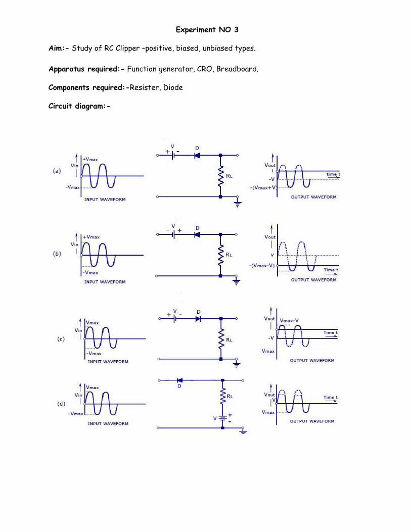
Experiment NO 3
Aim:- Study of RC Clipper –positive, biased, unbiased types.
Apparatus required:- Function generator, CRO, Breadboard.
Components required:-Resister, Diode
Circuit diagram:-

Theory:-
• Explain operation of different clipper circuits along with waveforms.
• What are the applications of clipper circuit?
Procedure:-
• Mount the components on bread board as per circuit diagram.
• Make connections as shown in figure.
• Give input from function generator.
• Observe output on CRO.
Conclusion:-
Different waveforms for various clipper circuits are observed.

Experiment NO 4
Aim:- Study of RC Clamper –positive, biased, unbiased types.
Apparatus required:- Function generator, CRO, Breadboard.
Components required:-Capacitor, Diode

Theory:-
• Explain operation of different clamper circuits along with waveforms.
• What are the applications of clamper circuits?
Procedure:-
• Mount the components on bread board as per circuit diagram.
• Make connections as shown in figure.
• Give input from function generator.
• Observe output on CRO.
Conclusion:-
Different waveforms for various clamper circuits are observed.

Experiment NO 5
Aim:- Study of transistorized astable multivibrator.
Apparatus required:- Function generator, CRO, Breadboard.
Components required:-Capacitor C1 (0.1uF), Resistor R1=R4(1Kohm)R2=R3(10Kohm), and
Transistors(BC 107)
Theory:-
1. Explain operation of astable multivibrator circuit along with waveforms.
2. What are the applications of multivibrator circuit?
Procedure:-
• Mount the components on bread board as per circuit diagram.
• Make connections as shown in figure.
• Give input from function generator.
• Observe output on CRO.
Observation:-
Theoretical value of time period = 1.38RC =………………….
Practical value of time period = ………………………………..
Conclusion:-
In an astable multivibrator circuit both transistors are not in ON or OFF state. When one
transistor is ON another is OFF and vice versa. At the collector of the transistors square
waveforms are formed with alternate ON and OFF transistor action.

Experiment NO 6
Aim: - To study the two stage RC Coupled Amplifier using Transistor.
Apparatus required: - Function generator, CRO, RC coupled Amplifier kit
Formula:-
AV=AV1*AV2
Where AV = Overall voltage gain.
AV1= Voltage gain of first stage.
Av2= Voltage gain of second stage.

Theory:-
Q. Explain working of R-C coupled amplifier
Procedure:-
1) Study the circuit provided on the front panel of the kit.
2) Connect the signal generator at the input terminals of the circuit.
3) Connect the CRO at the output of the fist stage.
4) Switch on the power supply.
5) Keep the input signal amplitude Vi constant so that transistors should not enter in
saturation. Now vary the input frequency Fi from 50 Hz to 100kHz in steps. Observe &
note the corresponding output voltage Vo . Find out the voltage gain Av.
6) Plot the graph between input frequency & voltage gain.
7) Observe & note the output voltage at collector of Q1.Caculate the gain of the first
stage AV1.
8) Observe & note the output voltage at collector of Q2.Caculate the gain of the first
stage AV2.
Observation Table:- Vin =_____V
For overall Gain
Sr. No I/P Frequency O/P Voltage Gain (Av)= Vo/Vin Gain (Av)in dB
For First Stage Vin =_____V
Sr. No I/P Frequency O/P Voltage Gain (Av) Gain (Av)in dB
For Second Stage Vin =_____V
Sr. No I/P Frequency O/P Voltage Gain (Av) Gain (Av)in dB
Result:-
AV1 = ---------, AV2 = ---------, AV = -------
Bandwidth of R-C Coupled amplifier is found to be ____________

Experiment NO 7
Aim :- To study of class A transformer coupled amplifier, its frequency response &
bandwidth.
Apparatus :- Signal Generator, CRO, Patch chords
Theory:-
Q. Explain working of Transformer coupled amplifier
Procedure:-
1. Study the circuit provided on the front panel of the kit.
2. Connect the signal generator at the input terminals.
3. Connect the CRO at the output terminals.
4. Switch on the power supply.
5. Apply a sine wave I/P around of 1KHz, Adjust the amplitude so that transistor should not
enter in saturation.
6. Now increase I/P frequency Fi from 100 Hz to 200 KHz in suitable steps, Observe &
note the corresponding O/P voltage VO. Determine it’s gain.
Plot the graph, frequency of I/P Fi VS gain. Determine its bandwidth.

Observations :-
Input voltage (Vi) = -------(constant)
Sr. No. I/P Frequency O/P Voltage Gain(vo/Vin) Gain in dB
Result :
The bandwidth of transformer coupled class A amplifier is found to be……..
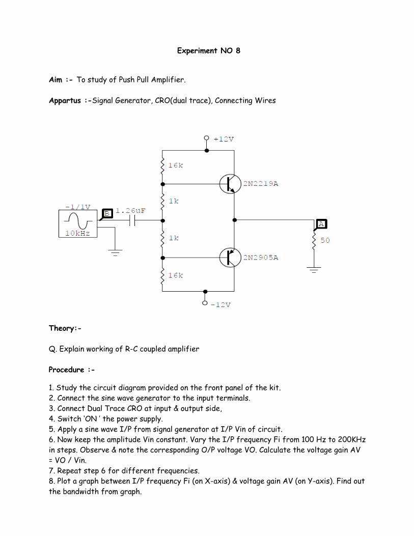
Experiment NO 8
Aim :- To study of Push Pull Amplifier.
Appartus :-Signal Generator, CRO(dual trace), Connecting Wires
Theory:-
Q. Explain working of R-C coupled amplifier
Procedure :-
1. Study the circuit diagram provided on the front panel of the kit.
2. Connect the sine wave generator to the input terminals.
3. Connect Dual Trace CRO at input & output side,
4. Switch ‘ON ’ the power supply.
5. Apply a sine wave I/P from signal generator at I/P Vin of circuit.
6. Now keep the amplitude Vin constant. Vary the I/P frequency Fi from 100 Hz to 200KHz
in steps. Observe & note the corresponding O/P voltage VO. Calculate the voltage gain AV
= VO / Vin.
7. Repeat step 6 for different frequencies.
8. Plot a graph between I/P frequency Fi (on X-axis) & voltage gain AV (on Y-axis). Find out
the bandwidth from graph.

Observations :-
Vin = --------V(constant)
Sr. No. I/P Frequency Output Voltage(Vo) Gain
Result:-
The frequency response of Class- B Push pull amplifier is studied having bandwidth
BW = --------- Hz.

Quiz:-
What is an amplifier?
Q: What device is used to convert direct current to alternating current?
Q: How does a digital meter’s display differ from an analog meter’s display?
Q: Holding resistance constant, how does increasing current in a circuit affect voltage?
Q: How would adding a 20-Ω resistor in parallel with a 100-Ω resistor change the reading
on an ammeter?
Q: When measuring DC voltage across a device with a multimeter, the meter indicates 0
volts. What is one possible explanation for this reading?
Q: What is the resistance of a lamp which draws 120 mA when connected to a 12.6-V
battery?
Q: How should a multimeter’s leads be connected when measuring resistance?
Q. Why is it important to maintain an impedance match from the source to the load when
sending signals?
a. to reduce external noise b. to keep the line balanced
c. to reduce reflected energy d. to reduce attenuation
Q. Which of the following is represented by the symbol XL?
a. impedance of a load b. reactance of a coil
c. resonant frequency of a filter d. output level of a source
Q. One coulomb-per-second is equal to one:
a. watt b. joule
c. volt d. ampere
Q. Which of the components is the symbol for a PNP bipolar transistor?
Q. The frequency of a signal is INVERSELY proportional to which of the following:
a. period b. amplitude
c. phase d. power

Q. The amount of useful output power provided by a device is 1.5 W. It is powered by a 48-
V supply with 100 mA of current. How much power is wasted in heat?
a. 1.5 W b. 2.1 W
c. 3.3 W d. 6.3 W
Q. As the efficiency of a device DECREASES, which of the following will INCREASE?
a. power output b. amplifier gain
c. heat output d. output impedance
Q. What is the peak voltage of a sine wave that measures 220 VAC rms?
a. 155 V b. 169 V
c. 311 V d. 440 V
Q. A 1-mW signal is attenuated at the rate of 5 dB/1,000ft. What is the power level into a
receiver that is 6,000 feet from the signal source?
a. -5 dBm b. -10 dBm
c. -20 dBm d. -30 dBm
Q. Which of the following is one of the functions performed by a diode?
a. filter b. amplifier
c. rectifier d. inverter
16. A transmission line is rated at 25 pF/ft. How much capacitance will one mile (5280 ft)
of this transmission line have?
a. 13,200 pF b. 13.2 nF
c. 132 nF d. 1.32 µF
4. Conduction of VIVA-VOCE Examinations: -
Teacher should conduct oral exams of the students with full preparation. Normally the
objective questions with guess are to be avoided. To make it meaningful, the questions
should be such that depth of the student in the subject is tested. Oral Exams are to be
conducted in co-cordial situation. Teachers taking oral exams should not have ill thoughts
about each other & courtesies should be offered to each other in case of opinion, which
should be critically suppressed in front of the students.
5. Evaluation and marking system: -
Basic honesty in the evaluation and marking system is essential and in the process impartial
nature of the evaluator is required in the exam system. It is a primary responsibility of the
teacher to see that right students who really put their effort &intelligence are correctly
awarded.
The marking pattern should be justifiable to the students without any ambiguity and
teacher should see that students are faced with just circumstance.
Related Documents