! #$%$&'( )*&+%,'&+- .$,/0$&1 2*- 3+45,$+1 !"#"$%& ()$*#+%$*, -"+./"$0 1 !*0"#) 2*+03*.$"4* Semiconductor Memories Jan M. Rabaey Anantha Chandrakasan Borivoje Nikolic December 20, 2002

Welcome message from author
This document is posted to help you gain knowledge. Please leave a comment to let me know what you think about it! Share it to your friends and learn new things together.
Transcript

!"#$%$&'(")*&+%,'&+-".$,/0$&12*- 3+45,$+1
!"#"$%&'()$*#+%$*,'-"+./"$01'!*0"#)'2*+03*.$"4*
SemiconductorMemories
Jan M. RabaeyAnantha ChandrakasanBorivoje Nikolic
December 20, 2002

!"#$%$&'(")*&+%,'&+-".$,/0$&12*- 3+45,$+1
!"#$%&'()*&'*+&,
Memory ClassificationMemory ArchitecturesThe Memory CorePeripheryReliabilityCase Studies

!"#$%$&'(")*&+%,'&+-".$,/0$&12*- 3+45,$+1
!"#$%&'()%*&+,-"#&+.,/0122$3$%1*$&'
Read-Write MemoryNon-VolatileRead-Write
Memory
Read-Only Memory
EPROM
E2PROM
FLASH
Random
AccessNon-Random
Access
SRAM
DRAM
Mask-Programmed
Programmable (PROM)
FIFO
Shift Register
CAM
LIFO

!"#$%$&'(")*&+%,'&+-".$,/0$&12*- 3+45,$+1
!"#$%&'()#)*+,'-".)*)/)$*0

!"#$%$&'(")*&+%,'&+-".$,/0$&12*- 3+45,$+1
!"#$%&'(%)*+,"),-%".'/")$0"%1
Word 0
Word 1
Word 2
WordN2 2
WordN2 1
Storagecell
M bits M bits
Nwords
S0
S1
S2
SN2 2
A0
A1
AK2 1
K 5 log2N
SN2 1
Word 0
Word 1
Word 2
WordN2 2
WordN2 1
Storagecell
S0
Input-Output(M bits)
Intuitive architecture for N x M memoryToo many select signals:
N words == N select signals K = log2NDecoder reduces the number of select signals
Input-Output(M bits)
Decoder
!"#$%$&'(")*&+%,'&+-".$,/0$&12*- 3+45,$+1
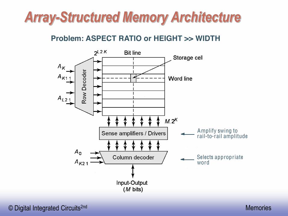
!""#$%&'"()'("*+,-*./"$,!")01'*)'("*Problem: ASPECT RATIO or HEIGHT >> WIDTH
Amplify swing torail-to-rail amplitude
Selects appropriateword

!"#$%$&'(")*&+%,'&+-".$,/0$&12*- 3+45,$+1
!"#$%$&'"&%()*#+,$-).$&'"/#&/0$#
Advantages:1. Shorter wires within blocks2. Block address activates only 1 block => power savings

!"#$%$&'(")*&+%,'&+-".$,/0$&12*- 3+45,$+1
!"#$%&'()#)*+,'-..%$/01"2
DRAM TimingMultiplexed Adressing
SRAM TimingSelf-timed

!"#$%$&'(")*&+%,'&+-".$,/0$&12*- 3+45,$+1
!"#$%&'()*+",-.)*/"((0
WL
BL
WL
BL
1WL
BL
WL
BL
WL
BL
0
VDD
WL
BL
GND
Diode ROM MOS ROM 1 MOS ROM 2
!"#$%$&'(")*&+%,'&+-".$,/0$&12*- 3+45,$+1
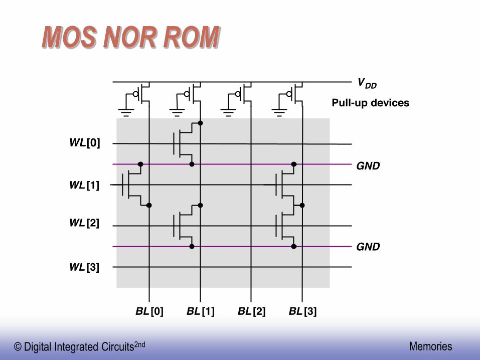
!"#$%"&$&"!
WL[0]
GND
BL [0]
WL [1]
WL [2]
WL [3]
VDD
BL [1]
Pull-up devices
BL [2] BL [3]
GND

!"#$%$&'(")*&+%,'&+-".$,/0$&12*- 3+45,$+1
!"#$%"&$&"!$'()*+,
Programmming using theActive Layer Only
Polysilicon
Metal1
Diffusion
Metal1 on Diffusion
Cell (9.5 x 7 )

!"#$%$&'(")*&+%,'&+-".$,/0$&12*- 3+45,$+1
!"#$%&%'$("!
All word lines high by default with exception of selected row
WL[0]
WL[1]
WL[2]
WL[3]
VDDPull-up devices
BL[3]BL[2]BL[1]BL [0]

!"#$%$&'(")*&+%,'&+-".$,/0$&12*- 3+45,$+1
!"#$%&%'$("!$)*+,-.
No contact to VDD or GND necessary;
Loss in performance compared to NOR ROMdrastically reduced cell size
Polysilicon
Diffusion
Metal1 on Diffusion
Cell (8 x 7 )
Programmming using
the Metal-1 Layer Only
!"#$%$&'(")*&+%,'&+-".$,/0$&12*- 3+45,$+1
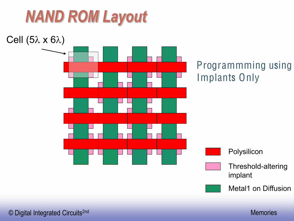
!"!#$%&'$()*+,-Cell (5 x 6 )
Polysilicon
Threshold-alteringimplant
Metal1 on Diffusion
Programmming using
Implants Only

!"#$%$&'(")*&+%,'&+-".$,/0$&12*- 3+45,$+1
!"#$"%&'()*+,$-*.'("*!"/%0
Metal bypass
Polysilicon word lineK cells
Polysilicon word lineWLDriver
(b) Using a metal bypass
(a) Driving the word line from both sides
Metal word line
WL
(c) Use silicides

!"#$%$&'(")*&+%,'&+-".$,/0$&12*- 3+45,$+1
!"#$%&"'#()*+,)-+.).+*
PMOS precharge device can be made as large as necessary,but clock driver becomes harder to design.
WL [0]
GND
BL [0]
WL [1]
WL [2]
WL [3]
VDD
BL [1]
Precharge devices
BL [2] BL [3]
GND
pref

!"#$%$&'(")*&+%,'&+-".$,/0$&12*- 3+45,$+1
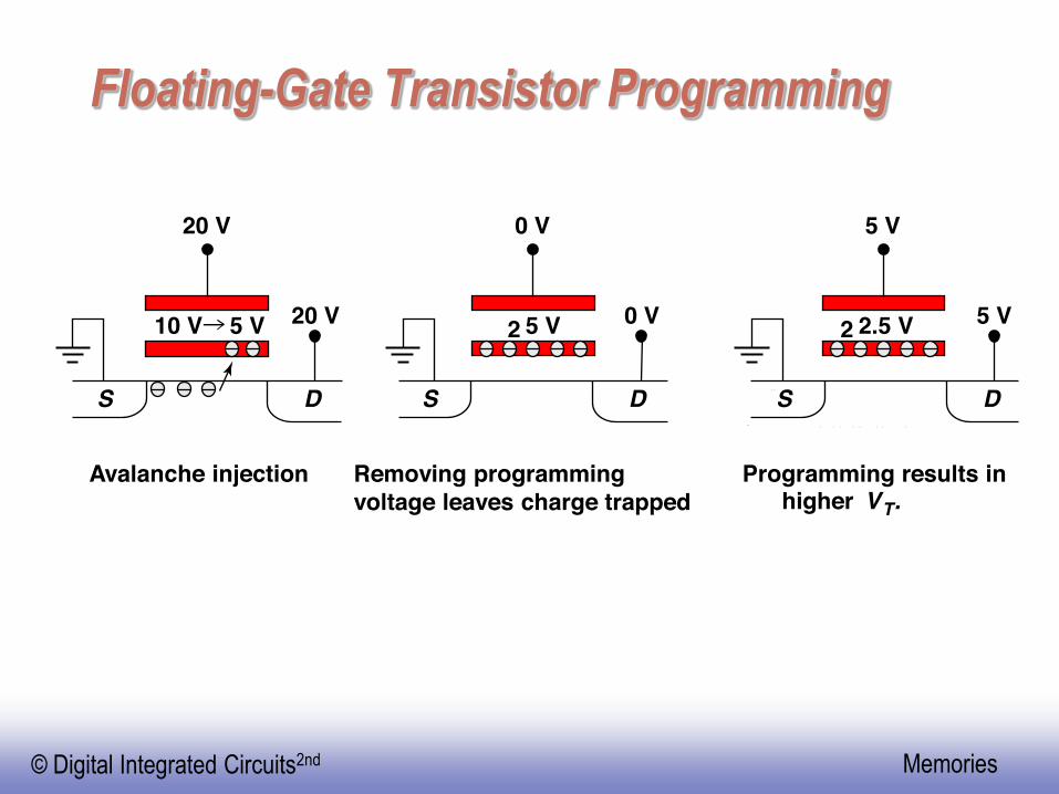
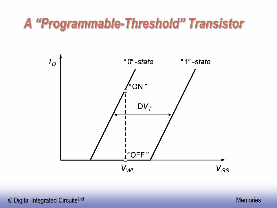
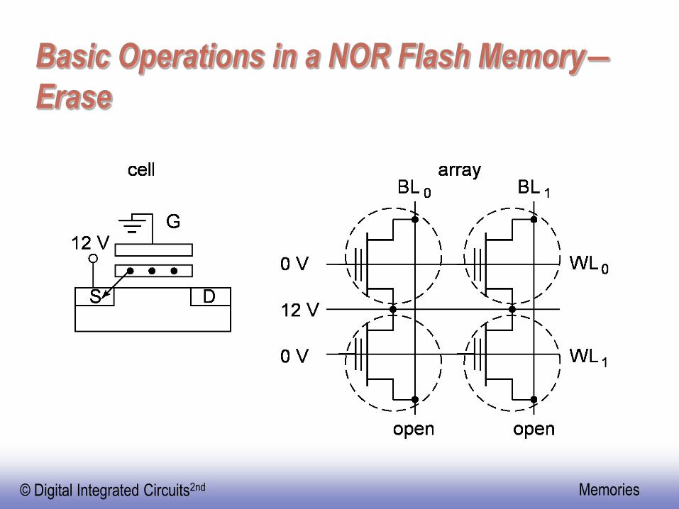
!"#$%"&'()&*+,*-".)*/01*+2&"'()#3$3'(*+(.'#/)/(".+425,678
Floating gate
Source
Substrate
Gate
Drain
n+ n+_p
toxtox
Device cross-section Schematic symbol
G
S
D
!"#$%$&'(")*&+%,'&+-".$,/0$&12*- 3+45,$+1
!"#$%&'()*$%+,-.$'/&/%#.,0.#(.$11&'(
0 V
2 5 V 0 V
DS
Removing programming voltage leaves charge trapped
5 V
2 2.5 V 5 V
DS
Programming results inhigher VT.
20 V
10 V 5 V 20 V
DS
Avalanche injection
!"#$%$&'(")*&+%,'&+-".$,/0$&12*- 3+45,$+1
!
!"#$%$&'(")*&+%,'&+-".$,/0$&12*- 3+45,$+1
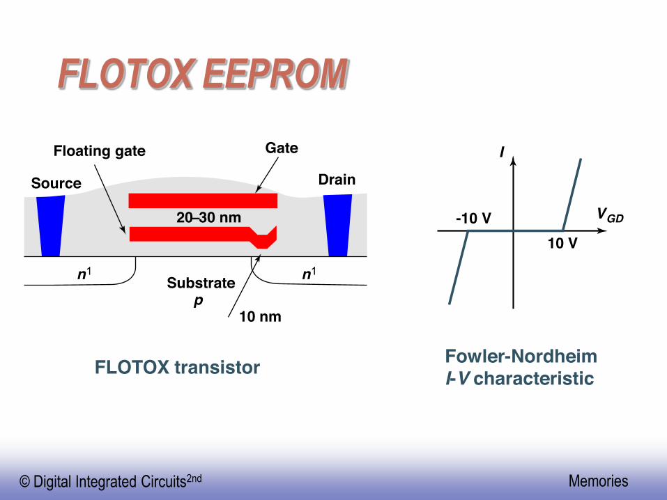
!"#$#%&''()#*Floating gate
Source
Substratep
Gate
Drain
n1 n1
FLOTOX transistor Fowler-Nordheim I-V characteristic
20 30 nm
10 nm
-10 V10 V
I
VGD

!"#$%$&'(")*&+%,'&+-".$,/0$&12*- 3+45,$+1
!!"#$%&'())
WL
BL
VDD
Absolute threshold controlis hardUnprogrammed transistor might be depletion
2 transistor cell

!"#$%$&'(")*&+%,'&+-".$,/0$&12*- 3+45,$+1
!"#$%&''()*+
Control gate
erasure
p-substrate
Floating gate
Thin tunneling oxide
n1 source n1 drainprogramming
!"#$%$&'(")*&+%,'&+-".$,/0$&12*- 3+45,$+1
!"#$%

!"#$%$&'(")*&+%,'&+-".$,/0$&12*- 3+45,$+1
!"#$%

!"#$%$&'(")*&+%,'&+-".$,/0$&12*- 3+45,$+1
!"#$
!"#$%$&'(")*&+%,'&+-".$,/0$&12*- 3+45,$+1
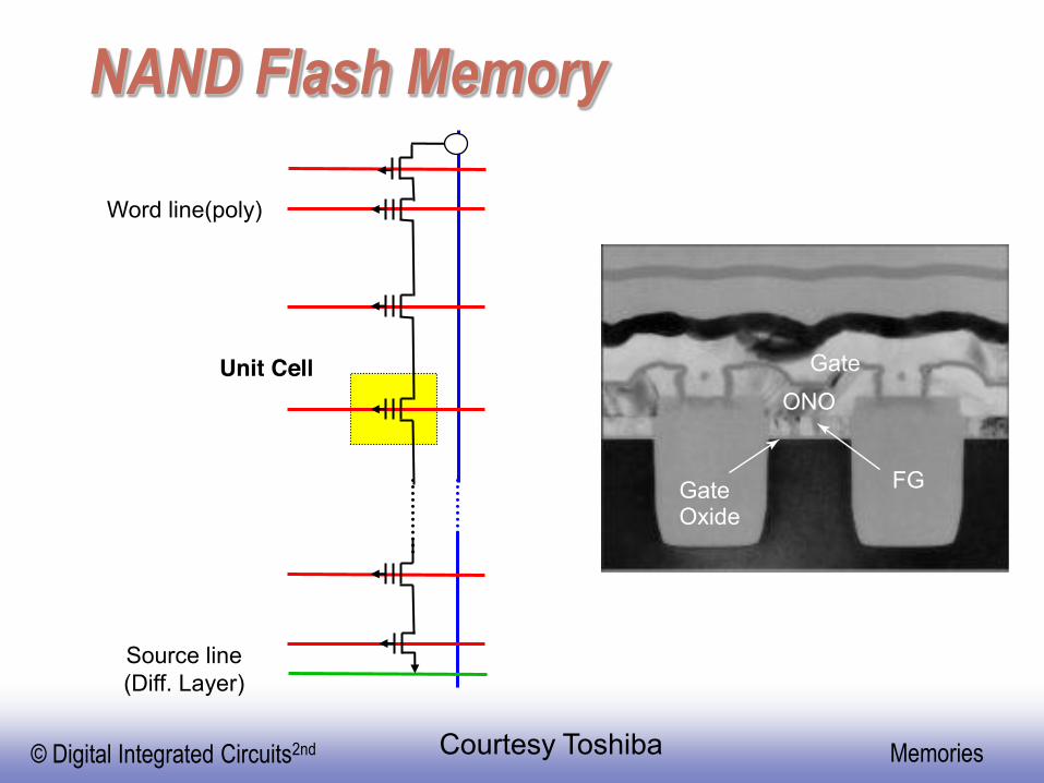
!"!#$%&'()$*+,-./
Unit Cell
Word line(poly)
Source line(Diff. Layer)
Courtesy Toshiba
GateONO
FGGateOxide

!"#$%$&'(")*&+%,'&+-".$,/0$&12*- 3+45,$+1
!"!#$%&'()$*+,-./
Word linesSelect transistor
Bit line contact Source line contact
Active area
ST I
Courtesy Toshiba
!"#$%$&'(")*&+%,'&+-".$,/0$&12*- 3+45,$+1
!"#$#%&'$()&(%)*+,*-&#&'.+,.&"'.#$&*/01
!"#$%$&'(")*&+%,'&+-".$,/0$&12*- 3+45,$+1
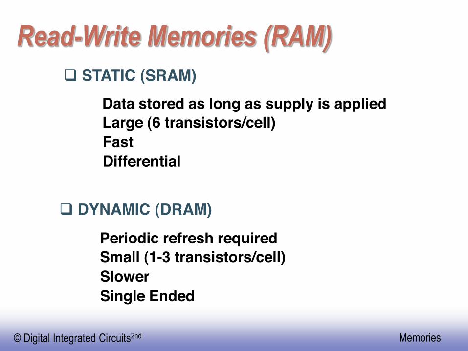
!"#$%&'()"*+",-'(".*/!0+1STATIC (SRAM)
DYNAMIC (DRAM)
Data stored as long as supply is appliedLarge (6 transistors/cell)FastDifferential
Periodic refresh requiredSmall (1-3 transistors/cell)SlowerSingle Ended

!"#$%$&'(")*&+%,'&+-".$,/0$&12*- 3+45,$+1
!"#$%&'('#)$*+,-.*./0,*+122*
WL
BL
VDD
M5M6
M4
M1
M2
M3
BL

!"#$%$&'(")*&+%,'&+-".$,/0$&12*- 3+45,$+1
!"#$%&'( )*+,-.(VDD
GND
WL
BLBL
M1 M3
M4M2
M5 M6

!"#$%$&'(")*&+%,'&+-".$,/0$&12*- 3+45,$+1
!"#$#%&'(")*+&,-.!/0-1"**
Static power dissipation -- Want R L largeBit lines precharged to V DD to address t p problem
M3
RL RLVDD
WL
Q Q
M1 M2
M4
BL BL

!"#$%$&'(")*&+%,'&+-".$,/0$&12*- 3+45,$+1
!"#$%&'()(*+,)-.+-*.
!"#$%$&'(")*&+%,'&+-".$,/0$&12*- 3+45,$+1
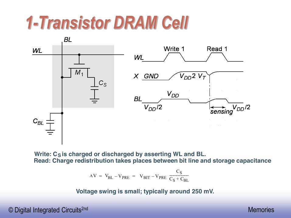
!"#$%&'(')*$+,-./+0122
Write: CS is charged or discharged by asserting WL and BL.Read: Charge redistribution takes places between bit line and storage capacitance
Voltage swing is small; typically around 250 mV.
V BL VPRE VBIT VPRECS
CS CBL+------------= =V
!"#$%$&'(")*&+%,'&+-".$,/0$&12*- 3+45,$+1
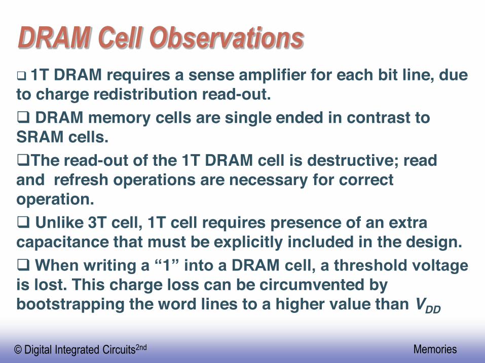
!"#$%&'((%)*+',-./012+1T DRAM requires a sense amplifier for each bit line, due
to charge redistribution read-out.DRAM memory cells are single ended in contrast to
SRAM cells.The read-out of the 1T DRAM cell is destructive; read
and refresh operations are necessary for correct operation.
Unlike 3T cell, 1T cell requires presence of an extra capacitance that must be explicitly included in the design.
1is lost. This charge loss can be circumvented by bootstrapping the word lines to a higher value than VDD

!"#$%$&'(")*&+%,'&+-".$,/0$&12*- 3+45,$+1
!"#$"%&'(%)("*+,-.#
DV(1)
V(1)
V(0)t
VPRE
VBL
Sense amp activatedWord line activated
!"#$%$&'(")*&+%,'&+-".$,/0$&12*- 3+45,$+1
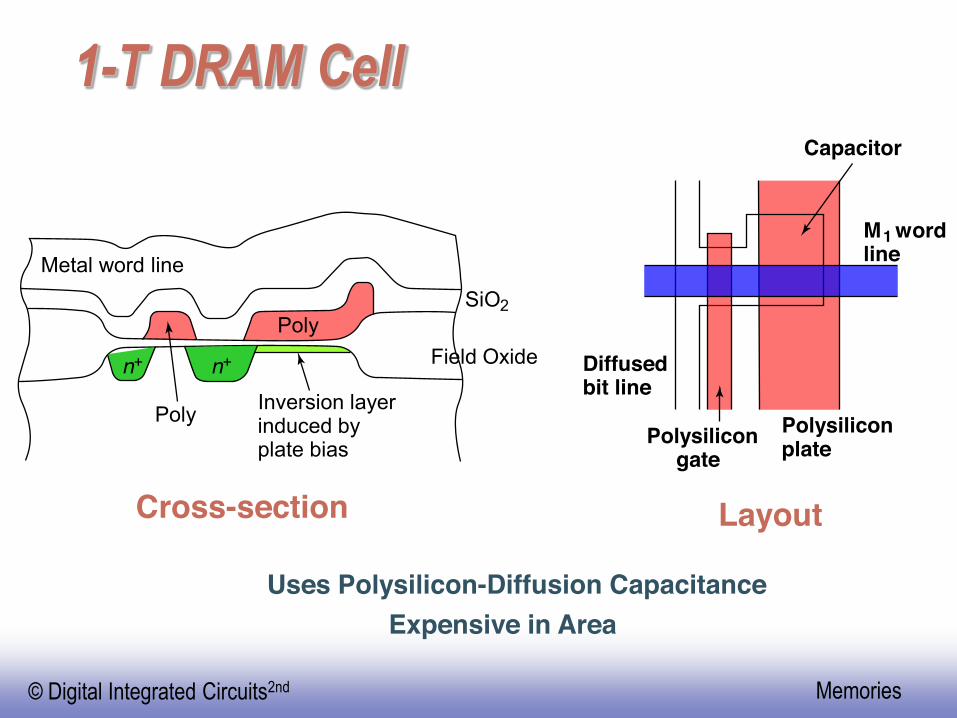
!"#$%&'($)*++
Uses Polysilicon-Diffusion CapacitanceExpensive in Area
M1 wordline
Diffusedbit line
Polysilicongate
Polysiliconplate
Capacitor
Cross-section Layout
Metal word line
Poly
SiO2
Field Oxiden+ n+
Inversion layerinduced byplate bias
Poly
!"#$%$&'(")*&+%,'&+-".$,/0$&12*- 3+45,$+1
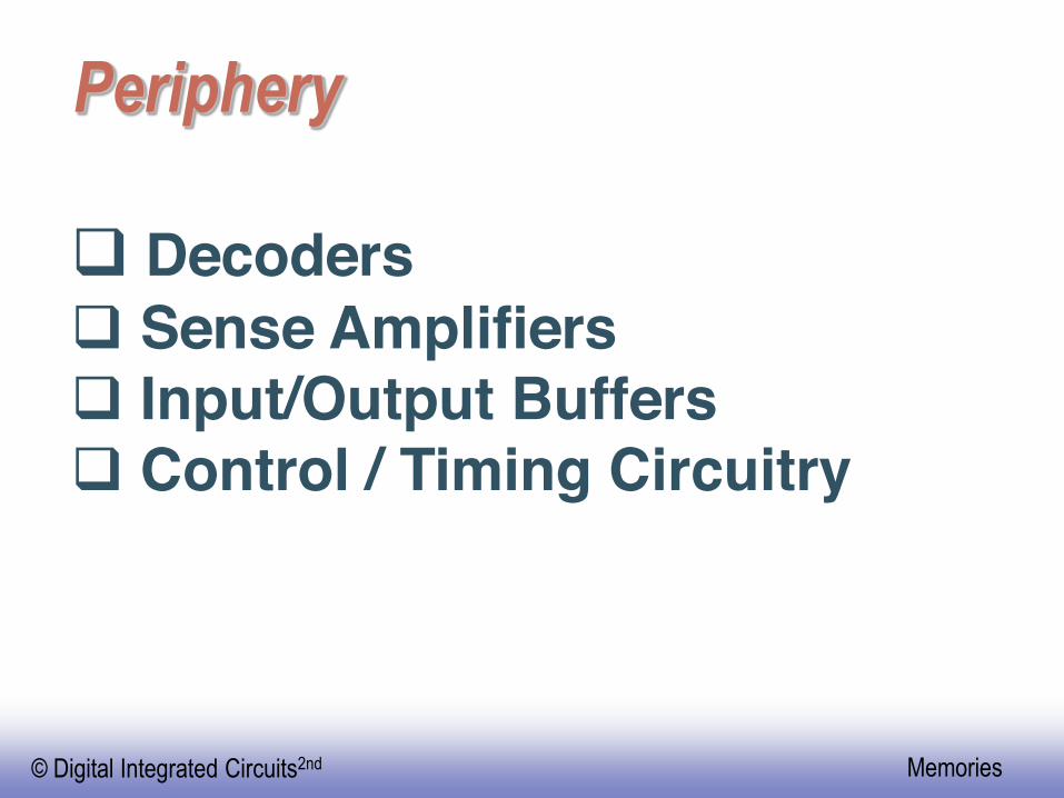
!"#$%&"#'
DecodersSense AmplifiersInput/Output BuffersControl / Timing Circuitry

!"#$%$&'(")*&+%,'&+-".$,/0$&12*- 3+45,$+1
!"#$%&'"(&)*Collection of 2M complex logic gatesOrganized in regular and dense fashion
(N)AND Decoder
NOR Decoder
!"#$%$&'(")*&+%,'&+-".$,/0$&12*- 3+45,$+1
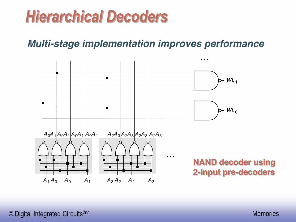
!"#$%$&'"&%()*#&+,#$-
A2A2
A2A3
WL 0
A2A3A2A3A2A3
A3 A3A0A0
A0A1A0A1A0A1A0A1
A1 A1
WL 1
Multi-stage implementation improves performance
NAND decoder using2-input pre-decoders

!"#$%$&'(")*&+%,'&+-".$,/0$&12*- 3+45,$+1
!"#$%&'(!)'*+),-
Precharge devices
VDD
GND
WL3
WL2
WL1
WL0
A0A0
GND
A1A1
WL3
A0A0 A1A1
WL 2
WL 1
WL 0
VDD
VDD
VDD
VDD
2-input NOR decoder 2-input NAND decoder

!"#$%$&'(")*&+%,'&+-".$,/0$&12*- 3+45,$+1
!"#$%&'(%)**"'+)$*#*',+(-)*./(0,1&2$(/.0,/.+
Advantages: speed (tpd does not add to overall memory access time)Only one extra transistor in signal path
Disadvantage: Large transistor count
2-input NOR decoder
A0S0
BL 0 BL 1 BL 2 BL 3
A1
S1
S2
S3
D
Related Documents
![0$1.-,-2()$#33$ 1.-,-2()$45/)+0$$ 1.5&65,()$7&8+2/59(/-.20 · PDF file$1,1#&/$*15,1*x"4"*-',=".*,1*,*.#$1,/="*&@*rpp*%*@4&%*15"*/"d1c='&$"$1*$1,1#&/;*05"*$"=&/.*."-'&)%"/1*'&=,1#&/*x,$*@3415"4*$&315",$1*#/*15"*1&x/*&@*]](https://static.cupdf.com/doc/110x72/5a72a19f7f8b9a93538de0ad/01-233-1-2450-156578259-20-nbsppdf.jpg)
![0)1'#$ · PDF file7ye frgf(v(j./4(]"&.l(w+..&(e.,-&"#"'6(7)+3()&:(g&.+'6(!)+1(=(%&,#@:%&'($"":(')/%f,)?"&()&:()&).+">%,(:%'./4.+(*#)](https://static.cupdf.com/doc/110x72/5a78f6017f8b9a217b8b4e6b/01-frgfvj4lwe-673g61f4.jpg)


![22 12 Umbruch PL - · PDF file= ]h ;>+! 9>* *> 9>* (*= >( # % & ! ! ( "&! ,'$ '# , &&& " " "](https://static.cupdf.com/doc/110x72/5a78aebd7f8b9a70648b4846/22-12-umbruch-pl-h-9-9-.jpg)


