Effect of Deposition Time on Structural and Optoelectronic Properties of Flower-Like Nanostructured PbS Thin Films N. H. Sheeba 1* , A. Namitha 2 , K. M. Ramsiya 2 , T. M. Ashitha 3 , R. Suhail 3 1 Department of Physics, M. E. S. Asmabi College, P. Vemballur, Kodungallur, 680671, India 2 Department of Physics, S. N. College, Nattika, Thriprayar, 680566, India 3 Department of Physics, M. E. S. Marampally College, Aluva, 683547, India Received 25 May 2020, accepted in final revised form 28 September 2020 Abstract Polycrystalline nanostructured PbS thin films are deposited onto soda-lime glass substrates by the method of chemical bath deposition (CBD) at different duration of deposition time. The structure and surface morphology of the films are characterized by X-ray diffraction (XRD) and field effect scanning electron microscopy (FE-SEM). XRD pattern exhibits polycrystalline structure with preferential orientation along (200) direction, parameters such as crystallite size, lattice constant, lattice-strain and dislocation density are calculated. The FE-SEM images show appearance of flower like structure on formation of PbS films which is indicative of suitability in gas sensing applications. Studies on optical properties carried out by UV-Vis spectroscopy measurements show bandgap in the range 1.65eV – 1.41eV. The photoluminescence spectra of the films exhibit two peaks centered at around 613 nm and 738 nm after excitation at 450 nm. Electrical studies from Hall measurements indicate the carrier concentration and mobility of the PbS samples corroborate the variations in the conductivity. Keywords: Thin films; Chemical synthesis; Crystal growth; Surface morphology; Hall effect. © 2021 JSR Publications. ISSN: 2070-0237 (Print); 2070-0245 (Online). All rights reserved. doi: http://dx.doi.org/10.3329/jsr.v13i1.47240 J. Sci. Res. 13 (1), 9-20 (2021) 1. Introduction Lead sulphide (PbS) belongs to binary IV-VI semiconductor material with direct narrow optical energy band gap which can be tuned between 0.41 eV to 3eV at 300 K [1]. The flexibility to vary the band gap in PbS makes it a better candidate in solar cell applications [2]. Further, it is one of the oldest and most common detection materials in various infrared detectors. It functions as a photon detector, responding directly to the photons of radiation, as opposed to thermal detectors [3,4]. The large Bohr radius of 18 nm of the material leads to the observation of quantum confinement effects, a desirable property in * Corresponding author: [email protected] Available Online J. Sci. Res. 13 (1), 9-20 (2021) JOURNAL OF SCIENTIFIC RESEARCH www.banglajol.info/index.php/JSR Publications

Welcome message from author
This document is posted to help you gain knowledge. Please leave a comment to let me know what you think about it! Share it to your friends and learn new things together.
Transcript
Effect of Deposition Time on Structural and Optoelectronic Properties of
Flower-Like Nanostructured PbS Thin Films
N. H. Sheeba
1*, A. Namitha
2, K. M. Ramsiya
2, T. M. Ashitha
3, R. Suhail
3
1Department of Physics, M. E. S. Asmabi College, P. Vemballur, Kodungallur, 680671, India
2Department of Physics, S. N. College, Nattika, Thriprayar, 680566, India
3Department of Physics, M. E. S. Marampally College, Aluva, 683547, India
Received 25 May 2020, accepted in final revised form 28 September 2020
Abstract
Polycrystalline nanostructured PbS thin films are deposited onto soda-lime glass substrates
by the method of chemical bath deposition (CBD) at different duration of deposition time.
The structure and surface morphology of the films are characterized by X-ray diffraction
(XRD) and field effect scanning electron microscopy (FE-SEM). XRD pattern exhibits
polycrystalline structure with preferential orientation along (200) direction, parameters such
as crystallite size, lattice constant, lattice-strain and dislocation density are calculated. The
FE-SEM images show appearance of flower like structure on formation of PbS films which
is indicative of suitability in gas sensing applications. Studies on optical properties carried
out by UV-Vis spectroscopy measurements show bandgap in the range 1.65eV – 1.41eV.
The photoluminescence spectra of the films exhibit two peaks centered at around 613 nm
and 738 nm after excitation at 450 nm. Electrical studies from Hall measurements indicate
the carrier concentration and mobility of the PbS samples corroborate the variations in the
conductivity.
Keywords: Thin films; Chemical synthesis; Crystal growth; Surface morphology; Hall
effect.
© 2021 JSR Publications. ISSN: 2070-0237 (Print); 2070-0245 (Online). All rights reserved.
doi: http://dx.doi.org/10.3329/jsr.v13i1.47240 J. Sci. Res. 13 (1), 9-20 (2021)
1. Introduction
Lead sulphide (PbS) belongs to binary IV-VI semiconductor material with direct narrow
optical energy band gap which can be tuned between 0.41 eV to 3eV at 300 K [1]. The
flexibility to vary the band gap in PbS makes it a better candidate in solar cell applications
[2]. Further, it is one of the oldest and most common detection materials in various
infrared detectors. It functions as a photon detector, responding directly to the photons of
radiation, as opposed to thermal detectors [3,4]. The large Bohr radius of 18 nm of the
material leads to the observation of quantum confinement effects, a desirable property in
* Corresponding author: [email protected]
Available Online
J. Sci. Res. 13 (1), 9-20 (2021)
JOURNAL OF
SCIENTIFIC RESEARCH
www.banglajol.info/index.php/JSR
Publications
10 Flower-Like Nanostructured PbS Thin Films
the field of Dye Sensitized Solar Cells (DSSC) [5]. By many years, there has been an
increasing interest in the development of semiconductor gas sensors to their advantageous
features such as low cost, high sensitivity, fast response/recovery time, and simplicity in
device structure and circuitry [6,7]. There are few reports of PbS gas sensors which can
work at moderate operating temperatures unlike commonly used metal oxide gas sensors
in the range 200 to 650 °C as their operating temperatures [8,9]. It is well known that
among different preparation techniques such as SILAR [10], Sputtering [11], Spray
Pyrolysis [12] etc. the method of chemical bath deposition (CBD) is the most inexpensive
technique for PbS thin films which is based on the reaction of the species on the substrate
surface from aqueous solutions [13,14].
Even though PbS is a widely investigated material due to its varied applications, the
field of gas sensors is a less explored area [15-17]. The desired characteristic of a thin film
as a gas sensor is the roughness of the surface with large surface area. Such a surface can
provide adsorption sites by oxygen vacancies trapped within the surface which is
conducive to good sensor performance [18]. In this work, we present the morphology
evolution of PbS thin films with deposition time to form a surface with flower-like
structure using the cost effective method of Chemical Bath Deposition technique (CBD).
Further, the essential requisite of a sensor material need to be balanced with the
processing costs for practical applications. There are many reports of chemically
synthesized PbS thin films with characterization of their significant properties [19,20].
But to the best of our knowledge, PbS thin films with a morphology of flower-like
structure is rarely reported. The present work aims to study the micro-structure, surface
morphology, optical characteristics, photoluminescence and electrical parameters of PbS
thin films indicating the suitability of the material in gas sensor applications based on its
surface morphology and as absorber material in DSSC.
2. Experimental
Pure PbS thin films are grown on cleaned soda lime glass substrates via chemical bath
deposition technique. The chemicals used for the preparation of PbS thin films consist of
lead acetate [Pb(CH3COO)2.3H2O] (Merck, India), thiourea [(H2N)2CS], sodium
hydroxide (NaOH, Merck, India) and triethylene amine (TEA). The reagents are of
analytical grade and used without further purification. The precursor solution consists of
3.5 mL 2M NaOH, 3.0 mL of 1M thiourea and 2.5 mL of 0.5M lead acetate together
diluted to 50 mL with two drops of TEA. Cleaned glass substrates are then inserted
vertically into the beaker at different dipping times such as 1, 3 and 6 h, respectively. For
the convenience of discussion, the as-prepared PbS films are designated as PbS-1, PbS-2
and PbS-3 corresponding to the deposition times. The reaction process for forming PbS
films is described elsewhere [21].
The structural properties of the as-prepared PbS films are investigated using X-ray
diffraction, XRD (Bruker AXS D8 (USA) Advance X-ray diffractometer with Cu Kα
radiation λCu = 0.154056 nm as the source) and surface morphology using Field Effect
N. H. Sheeba et al., J. Sci. Res. 13 (1), 9-20 (2021) 11
Scanning Electron Microscope, FE-SEM (Sigma 300 HV FESEM, Germany). The optical
transmittance and absorbance have been recorded by Model: Varian, Cary 5000 UV–Vis
spectrophotometer, (Australia). Photoluminescence spectra of PbS samples are recorded
using Model: Fluoromax-4C spectro-fluorometer (Japan) with the excitation wavelength
of 450 nm. The Hall measurements have been carried out by four-probe method at room
temperature using ECOPIA Hall effect measurement system (HMS-3000 Ecopia, South
Korea) in a magnetic field strength of 0.54T.
3. Results and Discussion
3.1. Structural characterization
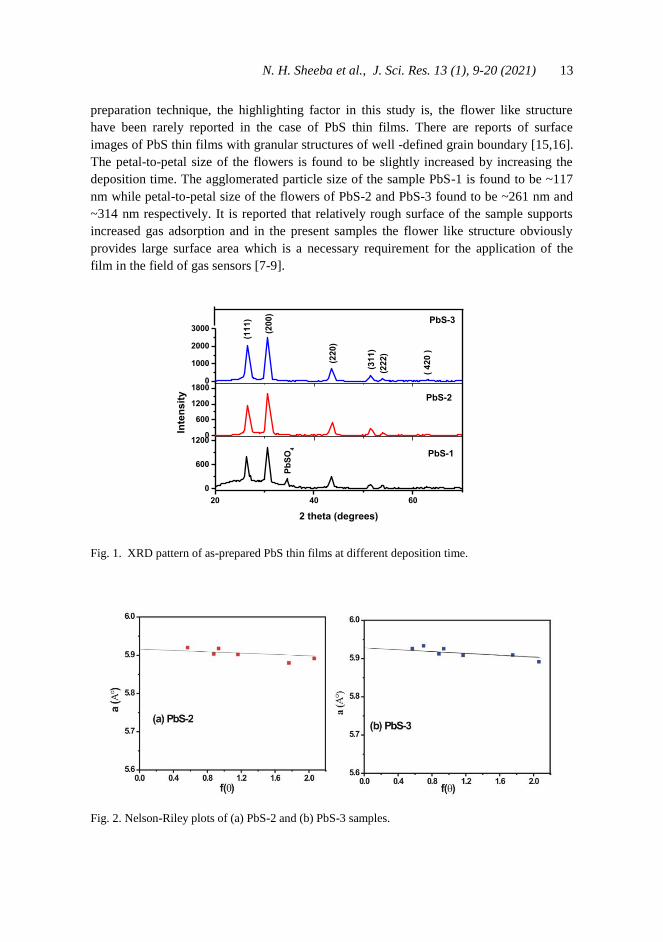
The XRD spectra of the as-prepared PbS nano crystalline thin films at different growth
time are shown in Fig. 1. All the synthesized PbS thin films have cubic rock salt (NaCl)
type structure (JCPDS cards No. 1-880) and the patterns contain peaks that are clearly
distinguishable. In the sample PbS-1, the diffraction peaks are observed at angles around
26°, 30°, 43°, 51° and 53° that correspond to the (111), (200), (220), (311) and (222)
planes of cubic PbS as confirmed by standard card with an extra peak at 34°. This
corresponds to peak of lead sulphate (PbSO4) (JCPDS 82-1855) which indicates the
formation of PbS is incomplete at this stage of deposition. In PbS-2 this diffraction peak
vanishes, retaining all the peaks corresponding to PbS and the intensity is found slightly
increased from that of PbS-1. The sample PbS-3 display characteristic PbS peaks with
higher intensity which is indicative of improved crystalline structure [22,23]. Moreover,
the absence of any other peaks corresponding to metallic clusters or impurities supports
the quality of samples [18]. All PbS films exhibit preferential orientation along (200)
direction. Table 1 illustrates the crystallite size of the PbS samples which is not affected
appreciably with growth time. The average crystallite size is calculated using well-known
Scherrer formula [24].
D =
(1)
where λ is the wavelength used (0.154 nm), β is the angular line width at half
maximum intensity and θ the Bragg angle.
The PbS-2 sample exhibits a small decrease in crystallite size, but as dip time increases
a tendency for growth in crystallite size is noticed. This must be due to the effect of
increase in thickness after the formation of pure PbS crystals. The dislocation density
which is a measure of number of dislocation lines per unit volume has been calculated
using equation [22].
(2)
12 Flower-Like Nanostructured PbS Thin Films
For all samples, the variation of 𝞭 is in accordance with that in crystallite size. The lattice
constant ‘a’ of the cubic rock salt has been computed for each peak using the formula
[11].
√ (3)
where h, k and l are Miller indices and d the inter-lattice spacing. In order to obtain more
accurate value of lattice constants free from all systematic errors, the iterative technique of
Nelson– Riley plots are employed. These are plots of the error function versus calculated
values of lattice constant for different planes. The corrected values of lattice constant ‘a’
is estimated from Nelson-Riley plots of ‘a’ versus error function f(θ) [25]. The
extrapolation to θ = 90° extracts the correct value of lattice constant ‘a’.
( )
] (4)
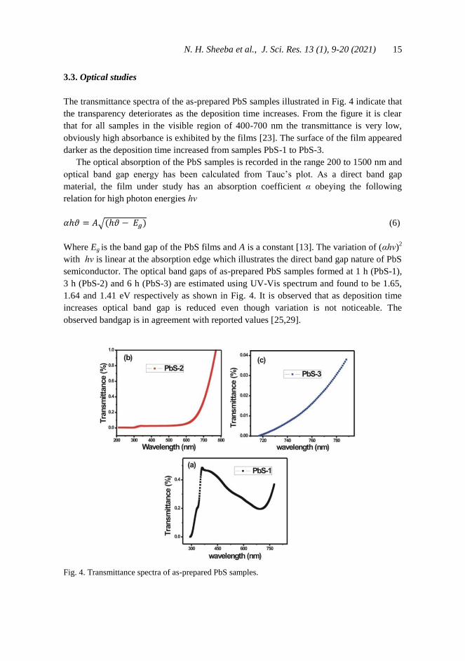
Fig. 2 depicts Nelson-Riley plots for pure PbS samples PbS-2 and PbS-3 and the value
of lattice constant ‘a’ indicate that it is improved and approaches the bulk value of 5.936
(A°) when deposition time increased from 3 h to 6 h [10,13]. But the deviation from the
bulk value suggests that the films are strained [26].
The lattice strain is calculated from the prominent peak using the relation [22]:
(5)
The values of strain illustrated in Table 1 indicate that on the formation PbS crystals,
strain decreases with increase in dip time which reflects relaxation of thicker films. In the
present work, among the samples, PbS-2 exhibits increase in dislocation density as the
particle size decreases which leads to strain-hardening. This implies that lattice strain in
PbS-2 film restricts the increase in particle size at the grain boundaries. Meanwhile the
lower value of strain and high intensity in diffraction pattern for PbS-3 is indicative of the
increased thickness with deposition time which comes in agreement with reported results
[22,25].
3.2. Surface morphology
The morphology of nano crystalline PbS thin film has been investigated using FE-SEM
which is shown in Fig. 3. It has been observed that the sample PbS-1 formed at a growth
time of 1 h possesses a surface with uniform grains, but has some voids and small cracks.
As from the XRD data of the sample, the formation of PbS thin film is incomplete at this
deposition time. A close observation of the image indicates the tendency to the formation
of flake like structure while the samples PbS-2 and PbS-3 illustrate surfaces with thickly
covered particles in the form of flakes and protruding flower like structure. The diffraction
peaks illustrate that at this deposition time the samples PbS-2 and PbS-3 represent pure
PbS material. Even though the formation of flower like structure is characteristic of this
N. H. Sheeba et al., J. Sci. Res. 13 (1), 9-20 (2021) 13
preparation technique, the highlighting factor in this study is, the flower like structure
have been rarely reported in the case of PbS thin films. There are reports of surface
images of PbS thin films with granular structures of well -defined grain boundary [15,16].
The petal-to-petal size of the flowers is found to be slightly increased by increasing the
deposition time. The agglomerated particle size of the sample PbS-1 is found to be ~117
nm while petal-to-petal size of the flowers of PbS-2 and PbS-3 found to be ~261 nm and
~314 nm respectively. It is reported that relatively rough surface of the sample supports
increased gas adsorption and in the present samples the flower like structure obviously
provides large surface area which is a necessary requirement for the application of the
film in the field of gas sensors [7-9].
0
1000
2000
3000
20 40 60
0
600
12000
600
1200
1800
PbS-3
(11
1)
(20
0)
(22
0)
(31
1)
(22
2)
( 4
20
)
2 theta (degrees)
PbS-1
Pb
SO
4
Inte
nsit
y PbS-2
Fig. 1. XRD pattern of as-prepared PbS thin films at different deposition time.
Fig. 2. Nelson-Riley plots of (a) PbS-2 and (b) PbS-3 samples.

14 Flower-Like Nanostructured PbS Thin Films
Table 1. Comparison of crystallographic data for as-prepared PbS thin films.
The formation of flower-like structure can be elucidated based on the growth kinetics.
Prolonged deposition time leads to increase in density of grains. On the thermodynamics
point of view, the surface growth shows the tendency to maintain the surface energy to the
minimum. In the present case, as deposition time increases, the larger number of grains
formed are likely to aggregate and form flakes as illustrated by FE-SEM. Further, the
neighbouring flakes agglomerate and self- assemble to form flower like structure to have
minimum surface energy by reducing the exposed areas. The PbS samples exhibit a
gradual evolution of morphology leading to the formation of flower-like structure as
deposition time increases from 1 h to 6 h. From diffraction pattern of the samples, it is
possible to infer that PbS flowers grow along (200) plane [27,28].
Fig. 3. FE-SEM micrographs of as-deposited PbS samples (a) PbS-1 (b) PbS-2 (c) PbS-3.
Sample
Crystallite size
D (nm)
Dislocation density
𝞭x1015(m-2) Lattice parameter
a (A°)
Strain εx10-3
PbS-1 21 2.3 - 1.66
PbS-2 18 3.1 5.92 1.94
PbS-3 21 2.3 5.93 1.68
N. H. Sheeba et al., J. Sci. Res. 13 (1), 9-20 (2021) 15
3.3. Optical studies
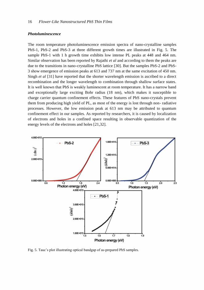
The transmittance spectra of the as-prepared PbS samples illustrated in Fig. 4 indicate that
the transparency deteriorates as the deposition time increases. From the figure it is clear
that for all samples in the visible region of 400-700 nm the transmittance is very low,
obviously high absorbance is exhibited by the films [23]. The surface of the film appeared
darker as the deposition time increased from samples PbS-1 to PbS-3.
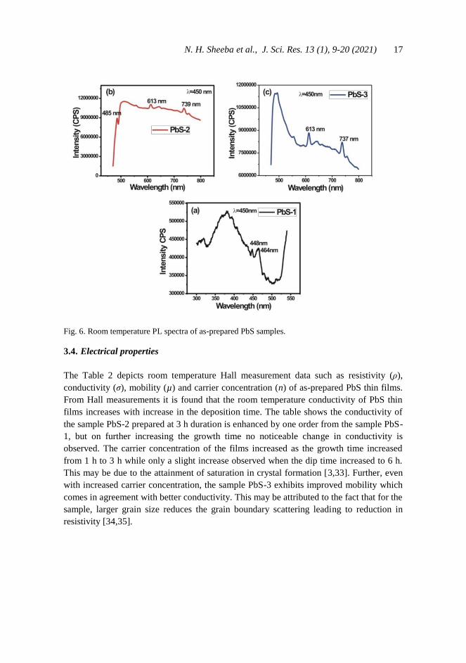
The optical absorption of the PbS samples is recorded in the range 200 to 1500 nm and
optical band gap energy has been calculated from Tauc’s plot. As a direct band gap
material, the film under study has an absorption coefficient α obeying the following
relation for high photon energies hν
√( ) (6)
Where Eg is the band gap of the PbS films and A is a constant [13]. The variation of (αhν)2
with hν is linear at the absorption edge which illustrates the direct band gap nature of PbS
semiconductor. The optical band gaps of as-prepared PbS samples formed at 1 h (PbS-1),
3 h (PbS-2) and 6 h (PbS-3) are estimated using UV-Vis spectrum and found to be 1.65,
1.64 and 1.41 eV respectively as shown in Fig. 4. It is observed that as deposition time
increases optical band gap is reduced even though variation is not noticeable. The
observed bandgap is in agreement with reported values [25,29].
Fig. 4. Transmittance spectra of as-prepared PbS samples.
16 Flower-Like Nanostructured PbS Thin Films
Photoluminescence
The room temperature photoluminescence emission spectra of nano-crystalline samples
PbS-1, PbS-2 and PbS-3 at three different growth times are illustrated in Fig. 5. The
sample PbS-1 with 1 h growth time exhibits low intense PL peaks at 448 and 464 nm.
Similar observation has been reported by Rajathi et al and according to them the peaks are
due to the transitions in nano-crystalline PbS lattice [30]. But the samples PbS-2 and PbS-
3 show emergence of emission peaks at 613 and 737 nm at the same excitation of 450 nm.
Singh et al [31] have reported that the shorter wavelength emission is ascribed to a direct
recombination and the longer wavelength to combination through shallow surface states.
It is well known that PbS is weakly luminescent at room temperature. It has a narrow band
and exceptionally large exciting Bohr radius (18 nm), which makes it susceptible to
charge carrier quantum confinement effects. These features of PbS nano-crystals prevent
them from producing high yield of PL, as most of the energy is lost through non- radiative
processes. However, the low emission peak at 613 nm may be attributed to quantum
confinement effect in our samples. As reported by researchers, it is caused by localization
of electrons and holes in a confined space resulting in observable quantization of the
energy levels of the electrons and holes [21,32].
Fig. 5. Tauc’s plot illustrating optical bandgap of as-prepared PbS samples.
N. H. Sheeba et al., J. Sci. Res. 13 (1), 9-20 (2021) 17
Fig. 6. Room temperature PL spectra of as-prepared PbS samples.
3.4. Electrical properties
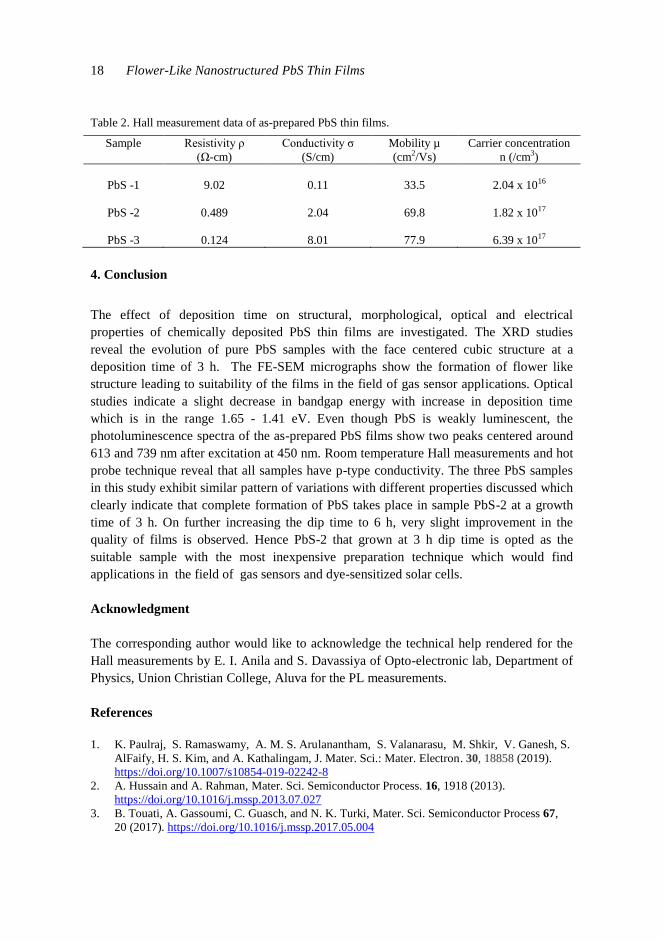
The Table 2 depicts room temperature Hall measurement data such as resistivity (ρ),
conductivity (σ), mobility (µ) and carrier concentration (n) of as-prepared PbS thin films.
From Hall measurements it is found that the room temperature conductivity of PbS thin
films increases with increase in the deposition time. The table shows the conductivity of
the sample PbS-2 prepared at 3 h duration is enhanced by one order from the sample PbS-
1, but on further increasing the growth time no noticeable change in conductivity is
observed. The carrier concentration of the films increased as the growth time increased
from 1 h to 3 h while only a slight increase observed when the dip time increased to 6 h.
This may be due to the attainment of saturation in crystal formation [3,33]. Further, even
with increased carrier concentration, the sample PbS-3 exhibits improved mobility which
comes in agreement with better conductivity. This may be attributed to the fact that for the
sample, larger grain size reduces the grain boundary scattering leading to reduction in
resistivity [34,35].
18 Flower-Like Nanostructured PbS Thin Films
Table 2. Hall measurement data of as-prepared PbS thin films.
Sample Resistivity ρ
(Ω-cm)
Conductivity σ
(S/cm)
Mobility µ
(cm2/Vs)
Carrier concentration
n (/cm3)
PbS -1
9.02
0.11
33.5
2.04 x 10¹⁶
PbS -2
0.489
2.04
69.8
1.82 x 10¹⁷
PbS -3
0.124
8.01
77.9
6.39 x 10¹⁷
4. Conclusion
The effect of deposition time on structural, morphological, optical and electrical
properties of chemically deposited PbS thin films are investigated. The XRD studies
reveal the evolution of pure PbS samples with the face centered cubic structure at a
deposition time of 3 h. The FE-SEM micrographs show the formation of flower like
structure leading to suitability of the films in the field of gas sensor applications. Optical
studies indicate a slight decrease in bandgap energy with increase in deposition time
which is in the range 1.65 - 1.41 eV. Even though PbS is weakly luminescent, the
photoluminescence spectra of the as-prepared PbS films show two peaks centered around
613 and 739 nm after excitation at 450 nm. Room temperature Hall measurements and hot
probe technique reveal that all samples have p-type conductivity. The three PbS samples
in this study exhibit similar pattern of variations with different properties discussed which
clearly indicate that complete formation of PbS takes place in sample PbS-2 at a growth
time of 3 h. On further increasing the dip time to 6 h, very slight improvement in the
quality of films is observed. Hence PbS-2 that grown at 3 h dip time is opted as the
suitable sample with the most inexpensive preparation technique which would find
applications in the field of gas sensors and dye-sensitized solar cells.
Acknowledgment
The corresponding author would like to acknowledge the technical help rendered for the
Hall measurements by E. I. Anila and S. Davassiya of Opto-electronic lab, Department of
Physics, Union Christian College, Aluva for the PL measurements.
References
1. K. Paulraj, S. Ramaswamy, A. M. S. Arulanantham, S. Valanarasu, M. Shkir, V. Ganesh, S.
AlFaify, H. S. Kim, and A. Kathalingam, J. Mater. Sci.: Mater. Electron. 30, 18858 (2019).
https://doi.org/10.1007/s10854-019-02242-8
2. A. Hussain and A. Rahman, Mater. Sci. Semiconductor Process. 16, 1918 (2013).
https://doi.org/10.1016/j.mssp.2013.07.027
3. B. Touati, A. Gassoumi, C. Guasch, and N. K. Turki, Mater. Sci. Semiconductor Process 67,
20 (2017). https://doi.org/10.1016/j.mssp.2017.05.004
N. H. Sheeba et al., J. Sci. Res. 13 (1), 9-20 (2021) 19
4. A. B. Rohom, P. U. Londhe, P. R. Jadhav, G. R. Bhand, and N. B. Chaure, J. Mater. Sci.:
Mater. Electron. 28, 17107 (2017). https://doi.org/10.1007/s10854-017-7637-4
5. . uan . ichaels R. Roy . ohansson . berg A. Andruszkiewicz, X. Zhang, M.
Freitag, and E. M. J. Johansson, ACS Appl. Energy Mater. 3, 3157 (2020).
https://doi.org/10.1021/acsaem.0c00030
6. C. L. Johnson and J.W. Schwank, Sensors Actuators B 20, 55 (1994).
https://doi.org/10.1016/0925-4005(93)01162-W
7. George F. Fine, Leon M. Cavanagh, A. Afonja, and R. Binions, Sensors 10, 5469 (2010).
https://doi.org/10.3390/s100605469
8. H. Karami, M. Ghasemi, and S. Matini, Int. J. Electrochem. Sci. 8, 11661 (2013).
9. V. V. Burungale, R. S. Devan, and S. A. Pawar, Mater. Sci. -Poland 34, 204 (2016).
https://doi.org/10.1515/msp-2016-0001
10. K. N. C. Kumar, S. K. K. Basha, and G. S. Muhammad, Int. J. Chem. Technol. Res. 7, 2257
(2014).
11. H. Soetedjo, B. Siswanto, I. Aziz, and S. Sudjatmoko, J. Non-Oxide Glasses 9, 55 (2017).
12. M. G. Faraj, Am. J. Condensed Matter Phys. 5, 51 (2015).
13. D. K. Sonavane, S. K. Jare, R. V. Kathare, R. N. Bulakhe, and J. -J. Shim, Mater. Today:
Proceed. 5, 7743 (2018). https://doi.org/10.1016/j.matpr.2017.11.451
14. J. J. Valenzuela- ´auregui R. Ram´ırez-Bon, A. Mendoza-Galva´n, M. Sotelo-Lerma, Thin
Solid Films 441, 104 (2003). https://doi.org/10.1016/S0040-6090(03)00908-8
15. B. Abdallah, A. Ismail, H. Kashoua, and W. Zetoun, J. Nanomater. 2018, ID 1826959 (2018).
https://doi.org/10.1155/2018/1826959
16. E. Barrios-Salgado, Y. Rodr-guez-Lazcano, J. P. Pérez-Orozco, J. Colin, P. Altuzar, J. Campos,
and D. Quesada, Adv. Condensed Matter Phys. 2019, ID 5960587 (2019).
https://doi.org/10.1155/2019/5960587
17. M. M. Abbas, A. Ab-M. Shehab, N. -A. Hassan, A. -K. Al-Samuraee, Thin Solid Films 519,
4917 (2011). https://doi.org/10.1016/S0040-6090(03)00908-8
18. N. H. Sheeba, S. C. Vattappalam, G. S Okram, V. Sharma, P. V. Sreenivasan, S. Mathew, and
R. R. Philip, Mater. Res. Bull. 93, 130 (2017).
https://doi.org/10.1016/j.materresbull.2017.04.021
19. B. Abdallah, R. Hussein, N. AlKafri, and W. Zetoun, Iran. J. Sci. Technol., Transact. A: Sci.
43, 1371 (2019). https://doi.org/10.1007/s40995-019-00698-1
20. F. Solis-Pomar, A. F. Cruz, JL Menchaca, MF Meléndrez and E. Pérez-Tijerina, Mater. Res.
Express 5 (2018) ID 106403. https://doi.org/10.1088/2053-1591/aadac0
21. T. Tohidi and K. Jamshidi-Ghaleh, Appl. Phys. A 118, 1 (2014).
https://doi.org/10.1007/s00339-014-8823-3
22. A. N. Fouda, M. Marzook, H. M. Abd El-Khalek, S. Ahmed, E. A. Eid, and A. B. El Basaty,
Silicon 9, 809 (2015). https://doi.org/10.1007/s12633-015-9399-z
23. S. Seghaier, N. Kamouna, R. Brini, and A. B. Amara, Mater. Chem. Phys. 97, 71 (2006).
https://doi.org/10.1016/j.matchemphys.2005.07.061
24. F. Khatun, M. A. Gafur, M. S. Ali, M. S. Islam, and M. A. R. Sarker, J. Sci. Res. 6, 217 (2014).
https://doi.org/10.3329/jsr.v6i2.17900
25. M. P. Sarma and G. Wary, Int. Lett. Chem. Phys. Astronomy 74, 22 (2017).
https://doi.org/10.18052/www.scipress.com/ILCPA.74.22
26. N. Choudhury and B. K. Sarma, Bull. Mater. Sci. 32, 43 (2009).
https://doi.org/10.1007/s12034-009-0007-y
27. J. Qiu, B. Weng, L. Zhao, C. Chang, Z. Shi, X. Li, H. K. Kim and Y. H. Hwang, J. Nanomater.
2014, ID 281461 (2014). http://dx.doi.org/10.1155/2014/281461
28. G. Bakiyaraj and R. Dhanasekaran, Appl. Nanosci. 3, 125 (2013).
https://doi.org/10.1007/s13204-012-0075-y
29. A. Beggas, Z. Becer, R. Ahmim, and M. S. Aida, Defect Diffus. Forum 397, 125 (2019).
https://doi.org/10.4028/www.scientific.net/DDF.397.125

20 Flower-Like Nanostructured PbS Thin Films
30. S. Rajathi, K. Kirubavathi, K. Selvaraju, J. Taibah Univ. Sci. 11, 1296 (2017).
https://doi.org/10.1016/j.jtusci.2017.05.001
31. L. R. Singh, A. N. Singh, and S. B. Singh, Int. J. Lumines. Applicat. 5, 76 (2015).
32. K. V. Khot, S. S. Mali, N. B. Pawar, R. M. Mane, V. V. Kondalkar, V. B. Ghanwat, P. S. Patil,
C. K. Hong, J. H. Kim, J. Heo, and P. N. Bhosale, J. Mater. Sci.: Mater. Electron. 25, 3762
(2014). https://doi.org/10.1007/s10854-014-2087-8
33. F. Gode, O. Baglayan, and E. Guneri, Chalcogenide Letts. 12, 519 (2015).
34. S. Thirumavalavana, K. Mani, and S. S. Sagadevan, J. Nano- Electron. Phys. 7, ID 04024
(2015).
35. M. V. Frischbier, H. F. Wardenga, M. Weidner, O. Bierwagen, J. Jia, Y. Shigesato, and A.
Klein, Thin Solid Films 614, 62 (2016). https://doi.org/10.1016/j.tsf.2016.03.022
Related Documents


