IMPORTANT NOTICE Dear customer, As from August 2 nd 2008, the wireless operations of NXP have moved to a new company, ST-NXP Wireless. As a result, the following changes are applicable to the attached document. ● Company name - Philips Semiconductors is replaced with ST-NXP Wireless. ● Copyright - the copyright notice at the bottom of each page “© Koninklijke Philips Electronics N.V. 200x. All rights reserved”, shall now read: “© ST-NXP Wireless 200x - All rights reserved”. ● Web site - http://www.semiconductors.philips.com is replaced with http://www.stnwireless.com ● Contact information - the list of sales offices previously obtained by sending an email to [email protected] , is now found at http://www.stnwireless.com under Contacts. If you have any questions related to the document, please contact our nearest sales office. Thank you for your cooperation and understanding. ST-NXP Wireless www.stnwireless.com

Welcome message from author
This document is posted to help you gain knowledge. Please leave a comment to let me know what you think about it! Share it to your friends and learn new things together.
Transcript

IMPORTANT NOTICE
Dear customer,
As from August 2nd 2008, the wireless operations of NXP have moved to a new company,ST-NXP Wireless.
As a result, the following changes are applicable to the attached document.
Company name - Philips Semiconductors is replaced with ST-NXP Wireless.
Copyright - the copyright notice at the bottom of each page “© Koninklijke Philips Electronics N.V. 200x. All rights reserved”, shall now read: “© ST-NXP Wireless 200x - All rights reserved”.
Web site - http://www.semiconductors.philips.com is replaced with http://www.stnwireless.com
Contact information - the list of sales offices previously obtained by sending an email to [email protected], is now found at http://www.stnwireless.com under Contacts.
If you have any questions related to the document, please contact our nearest sales office.Thank you for your cooperation and understanding.
ST-NXP Wireless
www.stnwireless.com

1. General description
The ISP1520 is a stand-alone Universal Serial Bus (USB) hub controller IC that complieswith Universal Serial Bus Specification Rev. 2.0. It supports data transfer at high-speed(480 Mbit/s), full-speed (12 Mbit/s) and low-speed (1.5 Mbit/s).
The upstream facing port can be connected to a Hi-Speed USB host or hub, or to anOriginal USB host or hub. If the upstream facing port is connected to a Hi-Speed USBhost or hub, then the ISP1520 will operate as a Hi-Speed USB hub. That is, it will supporthigh-speed, full-speed and low-speed devices connected to its downstream facing ports. Ifthe upstream facing port is connected to an Original USB host or hub, then the ISP1520will operate as an Original USB hub. That is, high-speed devices that are connected to itsdownstream facing ports will operate in full-speed mode instead.
The ISP1520 is a full hardware USB hub controller. All Original USB devices connected tothe downstream facing ports are handled using a single Transaction Translator (TT), whenoperating in a cross-version environment. This allows the whole 480 Mbit/s upstreambandwidth to be shared by all the Original USB devices on its downstream facing ports.
The ISP1520 has four downstream facing ports. If not used, ports 3 and 4 can bedisabled. The vendor ID, product ID and string descriptors on the hub are supplied by theinternal ROM; they can also be supplied by an external I2C-bus EEPROM or amicrocontroller.
The ISP1520 is suitable for self-powered hub designs.
An analog overcurrent detection circuitry is built into the ISP1520, which can also acceptdigital overcurrent signals from external circuits; for example, Micrel MOSFET switchMIC2026. The circuitry can be configured to trip on a global or an individual overcurrentcondition.
Each port comes with two status indicator LEDs.
Target applications of the ISP1520 are monitor hubs, docking stations for notebooks,internal USB hub for motherboards, hub for extending Intel Easy PCs, hub boxes, and soon.
ISP1520Hi-Speed Universal Serial Bus hub controllerRev. 04 — 28 April 2006 Product data sheet

Philips Semiconductors ISP1520Hi-Speed USB hub controller
2. Features
Complies with:
Universal Serial Bus Specification Rev. 2.0 Advanced Configuration and Power Interface (ACPI), OnNow and USB power
management requirements
Supports data transfer at high-speed (480 Mbit/s), full-speed (12 Mbit/s) andlow-speed (1.5 Mbit/s)
Self-powered capability
Configurable number of ports
Internal Power-On Reset (POR) and low voltage reset circuit
Port status indicators
Integrates high performance USB interface device with hub handler, Philips SerialInterface Engine (SIE) and transceivers
Built-in overcurrent detection circuit
Individual or ganged power switching, individual or global overcurrent protection, andnonremovable port support by I/O pins configuration
Simple I2C-bus (master or slave) interface to read device descriptor parameters,language ID, manufacturer ID, product ID, serial number ID and string descriptors froma dedicated external EEPROM, or to allow the microcontroller to set up hubdescriptors
Visual USB traffic monitoring (GoodLink) for the upstream facing port
Uses 12 MHz crystal oscillator with on-chip Phase-Locked Loop (PLL) for lowElectroMagnetic Interference (EMI)
Supports temperature range from −40 °C to +70 °C Available in LQFP64 package
3. Applications
Monitor hubs
Docking stations for notebooks
Internal hub for USB motherboards
Hub for extending Easy PCs
Hub boxes
4. Ordering information
Table 1. Ordering information
Type number Package
Name Description Version
ISP1520BD LQFP64 plastic low profile quad flat package; 64 leads; body 10 × 10 × 1.4 mm SOT314-2
ISP1520_4 © Koninklijke Philips Electronics N.V. 2006. All rights reserved.
Product data sheet Rev. 04 — 28 April 2006 2 of 53

xxxx xxxxxxxxxxxxxxxxxxxxxxxxxxxxxx x xxxxxxxxxxxxxx xxxxxxxxxx xxx xxxxxx xxxxxxxxxxxxxxxxxxxxxxx xxxxxxxxxxxxxxxxxxxxxxxxxxx xxxxxx xx xxxxxxxxxxxxxxxxxxxxxxxxxxxxx xxxxxxxxxxxxxxxxxxxxxx xxxxxxxxxxx xxxxxxx xxxxxxxxxxxxxxxxxxxxxxxxxxxxxxxxxxx xxxxxxxxxxxxxx xxxxxx xx xxxxxxxxxxxxxxxxxxxxxxxxxxxxxxxx xxxxxxxxxxxxxxxxxxxxxxxx xxxxxxxxxxxxxxxxxxxxxxxxxxxxxxxxxxxxxxxxxxxxxxxxxxxxx xxxxxxxxxxx xxxxx x x
ISP
1520_4
Product data shee
Philips S
emiconduc
5.B
lock diagramRAMROM
RPU DM0 DP0
2
12 MHzupstream port 0
XTAL1 XTAL2
RREF
34334375
t
BIT CLOCK
PLL
ANALOG TRANSCEIVER
VCC19, 39
13, 45
torsISP1520
Hi-S
peed US
B hub controller
004aaa169
I2C-BUSCONTROLLER
LINK LEDS
PORTCONTROLLER
HUBCONTROLLER
SDA
ADOC
NOOC
SCL
I C-bus
POWER SWITCH
VERCURRENT DETECTION
am
_N
PSW4_N
GRN4_N
AMB4_N
25 26 50 51
RESET_N
HUBGL_N
49
32
63
64
62
31
© K
oninklijke Philips E
lectronics N.V. 2006. A
ll rights reserved.
Rev. 04 —
28 April 2006
3 of 53
Fig 1. Block diagram
POWER SWITCH
OVERCURRENT DETECTION
LINK LEDS
RECOVERY
ANALOGTRANSCEIVER
− ORIGINAL USB− HI-SPEED USB
ROUTING LOGIC
PHILIPS PIE
PHILIPS SIE
MINI-HOSTCONTROLLER
HUB REPEATER− ORIGINAL USB− HI-SPEED USB
− ORIGINAL USB − HI-SPEED USB
TRANSACTIONTRANSLATOR
VCC2
VCC3
VCC4
VREF(5V0)
O
ANALOGTRANSCEIVER
− ORIGINAL USB− HI-SPEED USB
downstreamport 1
downstreamport 2 to port 3
downstreport 4
DM4DM1 DP1
OC1_N
PSW1_N
GRN1_N
AMB1_N DP4
ISP1520
OC4
15 16 19 20 60 61 47 48
GND
PORT 1 PORT 4PORTS 2 to 3
23, 57
11, 41
24, 56
TEST_HIGH
8, 12,18, 38
2, 6, 10,14, 21, 22, 35,40, 42,46, 58,59
TEST_LOW17
TEST1

Philips Semiconductors ISP1520Hi-Speed USB hub controller
6. Pinning information
6.1 Pinning
6.2 Pin description
Fig 2. Pin configuration
ISP1520BD
TEST DP4
GND DM4
DM0 GND
DP0 VCC2
RPU DP3
GND DM3
RREF GND
TEST_HIGH VCC4
VCC1 GND
GND VCC1
VCC4 TEST_HIGH
TEST_HIGH DP2
VCC2 DM2
GND GND
DM1 XTAL2
DP1 XTAL1
TE
ST
_LO
WS
DA
TE
ST
_HIG
HS
CL
OC
1_N
HU
BG
L_N
PS
W1_
NA
MB
1_N
GN
DG
RN
1_N
GN
DG
ND
VC
C3
GN
D
VR
EF
(5V
0)V
CC
3
OC
4_N
VR
EF
(5V
0)
PS
W4_
NA
MB
2_N
OC
3_N
GR
N2_
N
PS
W3_
NA
MB
3_N
OC
2_N
GR
N3_
N
PS
W2_
NA
MB
4_N
RE
SE
T_N
GR
N4_
N
AD
OC
NO
OC
004aaa164
1
2
3
4
5
6
7
8
9
10
11
12
13
14
15
16
48
47
46
45
44
43
42
41
40
39
38
37
36
35
34
33
17 18 19 20 21 22 23 24 25 26 27 28 29 30 31 32
64 63 62 61 60 59 58 57 56 55 54 53 52 51 50 49
Table 2. Pin description
Symbol [1] [2] Pin Type Description
TEST 1 - connect to ground through a 100 kΩ resistor
GND 2 - ground supply
DM0 3 AI/O upstream facing port D− connection (analog)
DP0 4 AI/O upstream facing port D+ connection (analog)
RPU 5 AI pull-up resistor connection; connect this pin through a resistor of1.5 kΩ ± 5 % to 3.3 V
GND 6 - ground supply
RREF 7 AI reference resistor connection; connect this pin through aresistor of 12 kΩ ± 1 % to an analog band gap ground reference
TEST_HIGH 8 - test pin; connect to 3.3 V
VCC1 9 - supply voltage 1 (3.3 V) (analog)
ISP1520_4 © Koninklijke Philips Electronics N.V. 2006. All rights reserved.
Product data sheet Rev. 04 — 28 April 2006 4 of 53

Philips Semiconductors ISP1520Hi-Speed USB hub controller
GND 10 - ground supply
VCC4 11 - supply voltage 4 (3.3 V) (crystal and PLL)
TEST_HIGH 12 - test pin; connect to 3.3 V
VCC2 13 - supply voltage 2 (3.3 V) (transceiver)
GND 14 - ground supply
DM1 15 AI/O downstream facing port 1 D− connection (analog)[3]
DP1 16 AI/O downstream facing port 1 D+ connection (analog)[3]
TEST_LOW 17 - connect to GND
TEST_HIGH 18 - connect to 5.0 V through a 10 kΩ resistor
OC1_N 19 AI/I overcurrent sense input for downstream facing port 1(analog/digital)
PSW1_N 20 I/O output — power switch control output (open-drain) with aninternal pull-up resistor for downstream facing port 1
input — function of the pin when used as an input is given inTable 5
GND 21 - ground supply
GND 22 - ground supply
VCC3 23 - supply voltage 3 (3.3 V) (digital)
VREF(5V0) 24 - reference voltage (5 V ± 5 %); used to power internal pull-upresistors of PSWn_N pins and also for the analog overcurrentdetection
OC4_N 25 AI/I overcurrent sense input for downstream facing port 4(analog/digital)
PSW4_N 26 I/O output — power switch control output (open-drain) with aninternal pull-up resistor for downstream facing port 4
input — function of the pin when used as an input is given inTable 5
OC3_N 27 AI/I overcurrent sense input for downstream facing port 3(analog/digital)
PSW3_N 28 I/O output — power switch control output (open-drain) with aninternal pull-up resistor for downstream facing port 3
input — function of the pin when used as an input is given inTable 5
OC2_N 29 AI/I overcurrent sense input for downstream facing port 2(analog/digital)
PSW2_N 30 I/O output — power switch control output (open-drain) with aninternal pull-up resistor for downstream facing port 2
input — function of the pin when used as an input is given inTable 5
RESET_N 31 I asynchronous reset input; when reset is active, the internalswitch to the 1.5 kΩ external resistor is opened, and all pinsDPn and DMn are 3-state; it is recommended that you connectto any one of the 3.3 V VCC pins through an RC circuit; refer tothe schematics in ISP1520 Hub Demo Board User’s Guide
ADOC 32 I analog or digital overcurrent detect selection input; LOW selectsdigital mode and HIGH (3.3 V or 5.0 V) selects analog mode
Table 2. Pin description …continued
Symbol [1] [2] Pin Type Description
ISP1520_4 © Koninklijke Philips Electronics N.V. 2006. All rights reserved.
Product data sheet Rev. 04 — 28 April 2006 5 of 53

Philips Semiconductors ISP1520Hi-Speed USB hub controller
XTAL1 33 I crystal oscillator input (12 MHz)
XTAL2 34 O crystal oscillator output (12 MHz)
GND 35 - ground supply
DM2 36 AI/O downstream facing port 2 D− connection (analog)[3]
DP2 37 AI/O downstream facing port 2 D+ connection (analog)[3]
TEST_HIGH 38 - test pin; connect to 3.3 V
VCC1 39 - supply voltage 1 (3.3 V) (analog)
GND 40 - ground supply
VCC4 41 - supply voltage 4 (3.3 V) (crystal and PLL)
GND 42 - ground supply
DM3 43 AI/O downstream facing port 3 D− connection (analog)[4]
DP3 44 AI/O downstream facing port 3 D+ connection (analog)[4]
VCC2 45 - supply voltage 2 (3.3 V) (transceiver)
GND 46 - ground supply
DM4 47 AI/O downstream facing port 4 D− connection (analog)[4]
DP4 48 AI/O downstream facing port 4 D+ connection (analog)[4]
NOOC 49 I no overcurrent protection selection input; connect this pin toHIGH (3.3 V) to select no overcurrent protection; if noovercurrent is selected, all OCn_N pins must be connected toVREF(5V0)
GRN4_N 50 I/O output — green LED port indicator (open-drain) fordownstream facing port 4
input — function of the pin when used as an input is given inTable 9
AMB4_N 51 I/O output — amber LED port indicator (open-drain) fordownstream facing port 4
input — function of the pin when used as an input is given inTable 8
GRN3_N 52 I/O output — green LED port indicator (open-drain) fordownstream facing port 3
input — function of the pin when used as an input is given inTable 9
AMB3_N 53 I/O output — amber LED port indicator (open-drain) fordownstream facing port 3
input — function of the pin when used as an input is given inTable 8
GRN2_N 54 I/O output — green LED port indicator (open-drain) fordownstream facing port 2
input — function of the pin when used as an input is given inTable 9
AMB2_N 55 I/O output — amber LED port indicator (open-drain) fordownstream facing port 2
input — function of the pin when used as an input is given inTable 8
Table 2. Pin description …continued
Symbol [1] [2] Pin Type Description
ISP1520_4 © Koninklijke Philips Electronics N.V. 2006. All rights reserved.
Product data sheet Rev. 04 — 28 April 2006 6 of 53

Philips Semiconductors ISP1520Hi-Speed USB hub controller
[1] The maximum current that the ISP1520 can sink on a pin is 8 mA.
[2] Symbol names ending with underscore N (for example, NAME_N) represent active LOW signals.
[3] Downstream ports 1 and 2 cannot be disabled.
[4] To disable a downstream port n, connect both pins DPn and DMn to VCC (3.3 V); unused ports must bedisabled in reverse order starting from port 4.
VREF(5V0) 56 - reference voltage (5 V ± 5 %); used to power internal pull-upresistors of PSWn_N pins and also for the analog overcurrentdetection
VCC3 57 - supply voltage 3 (3.3 V) (digital)
GND 58 - ground supply
GND 59 - ground supply
GRN1_N 60 I/O output — green LED port indicator (open-drain) fordownstream facing port 1
input — function of the pin when used as an input is given inTable 9
AMB1_N 61 I/O output — amber LED port indicator (open-drain) fordownstream facing port 1
input — function of the pin when used as an input is given inTable 8
HUBGL_N 62 O hub GoodLink LED indicator output; the LED is off until the hubis configured; a transaction between the host and the hub willblink the LED off for 100 ms
SCL 63 I/O I2C-bus clock (open-drain); see Table 11
SDA 64 I/O I2C-bus data (open-drain); see Table 11
Table 2. Pin description …continued
Symbol [1] [2] Pin Type Description
ISP1520_4 © Koninklijke Philips Electronics N.V. 2006. All rights reserved.
Product data sheet Rev. 04 — 28 April 2006 7 of 53

Philips Semiconductors ISP1520Hi-Speed USB hub controller
7. Functional description
7.1 Analog transceiversThe integrated transceivers directly interface to USB lines. They can transmit and receiveserial data at high-speed (480 Mbit/s), full-speed (12 Mbit/s) and low-speed (1.5 Mbit/s).
7.2 Hub controller coreThe main components of the hub core are:
• Philips Serial Interface Engine (SIE)
• Routing logic
• Transaction Translator (TT)
• Mini-Host Controller
• Hub repeater
• Hub controller
• Port controller
• Bit clock recovery
7.2.1 Philips serial interface engine
The Philips Serial Interface Engine (SIE) implements the full USB protocol layer. It iscompletely hardwired for speed and needs no firmware intervention. The functions of thisblock include: synchronization, pattern recognition, parallel or serial conversion, bit(de-)stuffing, CRC checking and generation, Packet IDentifier (PID) verification andgeneration, address recognition, and handshake evaluation and generation.
7.2.2 Routing logic
The routing logic directs signaling to appropriate modules (mini-Host Controller, OriginalUSB repeater and Hi-Speed USB repeater) according to the topology in which the hub isplaced.
7.2.3 Transaction translator
The Transaction Translator (TT) acts as a go-between mechanism that links devicesoperating in Original USB mode and Hi-Speed USB upstream mode. For the ‘IN’ direction,data is concatenated in TT buffers till the proper length is reached, before the host takesthe transaction. In the reverse direction (OUT), the mini-host dispenses the datacontained in TT buffers over a period that fits into the Original USB bandwidth. Thiscontinues until all outgoing data is emptied. TT buffers are used only on split transactions.
7.2.4 Mini-Host Controller
The internal mini-host generates all the Original USB IN, OUT or SETUP tokens for thedownstream facing ports, while the upstream facing port is in high-speed mode. Theresponses from Original USB devices are collected in TT buffers, until the end of thecomplete split transaction clears TT buffers.
ISP1520_4 © Koninklijke Philips Electronics N.V. 2006. All rights reserved.
Product data sheet Rev. 04 — 28 April 2006 8 of 53

Philips Semiconductors ISP1520Hi-Speed USB hub controller
7.2.5 Hub repeater
A hub repeater manages connectivity on a per packet basis. It implements packetsignaling connectivity and resume connectivity. There are two repeaters in the ISP1520: aHi-Speed USB repeater and an Original USB repeater. The only major difference betweenthese two repeaters is the speed at which they operate. When the hub is connected to anOriginal USB system, it automatically switches itself to function as an Original USB hub.
7.2.6 Hub and port controllers
The hub controller provides status report. The port controller provides control forindividual downstream facing ports; it controls the port routing module. Any port statuschange will be reported to the host using the hub status change (interrupt) endpoint.
7.2.7 Bit clock recovery
The bit clock recovery circuit extracts the clock from the incoming USB data stream.
7.3 Phase-locked loop clock multiplierA 12 MHz-to-480 MHz clock multiplier Phase-Locked Loop (PLL) is integrated on-chip.This allows the use of low-cost 12 MHz crystals. The low crystal frequency also minimizesEMI. No external components are required for the operation of the PLL.
7.4 I2C-bus controllerA simple serial I2C-bus interface is provided to transfer vendor ID, product ID and stringdescriptor from an external I2C-bus EEPROM or microcontroller. A master/slave I2C-busprotocol is implemented according to the timing requirements as mentioned in I2C-busstandard specifications. The maximum data count during I2C-bus transfers for theISP1520 is 256 B.
7.5 Overcurrent detection circuitAn overcurrent detection circuit is integrated on-chip. The main features of this circuit are:self reporting, automatic resetting, low-trip time and low cost. This circuit offers an easysolution at no extra hardware cost on the board.
7.6 GoodLinkIndication of a good USB connection is provided through the GoodLink technology. AnLED can be directly connected to pin HUBGL_N through an external 330 Ω resistor.
During enumeration, the LED momentarily blinks on. After successful configuration, theLED blinks off for 100 ms upon each transaction.
This feature provides a user-friendly indication of the status of the hub, the connecteddownstream devices, and the USB traffic. It is a useful diagnostics tool to isolate faultyUSB equipment, and helps to reduce field support and hotline costs.
7.7 Power-on resetThe ISP1520 has an internal Power-On Reset (POR) circuit.
ISP1520_4 © Koninklijke Philips Electronics N.V. 2006. All rights reserved.
Product data sheet Rev. 04 — 28 April 2006 9 of 53

Philips Semiconductors ISP1520Hi-Speed USB hub controller
The triggering voltage of the POR circuit is 2.03 V nominal. A POR is automaticallygenerated when VCC goes below the trigger voltage for a duration longer than 1 µs.
At t1: clock is running and available.
Fig 3. Power-on reset timing
Stable external clock is available at A.
Fig 4. External clock with respect to power-on reset
004aaa388
t1
VCC
2.03 V
0 V
≤ 683 µs
POR
POR
EXTERNAL CLOCK
A
004aaa365
ISP1520_4 © Koninklijke Philips Electronics N.V. 2006. All rights reserved.
Product data sheet Rev. 04 — 28 April 2006 10 of 53

Philips Semiconductors ISP1520Hi-Speed USB hub controller
8. Configuration selections
The ISP1520 is configured through I/O pins and, optionally, through an external I2C-bus,in which case the hub can update its configuration descriptors as a master or as a slave.
Table 3 shows configuration parameters.
[1] Multiple ganged power mode is reported as individual power mode; refer to Universal Serial Bus Specification Rev. 2.0.
[2] When the hub uses global overcurrent protection mode, the overcurrent indication is through wHubStatus field bit 1 (overcurrent) andthe corresponding change bit (overcurrent change).
8.1 Configuration through I/O pins
8.1.1 Number of downstream facing ports
To discount a physical downstream facing port, connect pins DP and DM of thatdownstream facing port to VCC (3.3 V), starting from the highest port number (4), seeTable 4.
The sum of physical ports configured is reflected in the bNbrPorts field.
Table 3. Configuration parameters
Mode and selection Option Configuration method
Pin control Software control
Control pin Reference Affected field Reference
Number of downstreamfacing ports
2 ports
3 ports
4 ports
DM1/DP1 toDM4/DP4
see Section 8.1.1 bNbrPorts0 see Table 22
Power switching mode ganged
multiple ganged[1]
individual
PSW1_N toPSW4_N
see Section 8.1.2 wHubCharacteristics:bits D1 and D0
see Table 22
bPwrOn2PwrGood:time interval
Overcurrent protectionmode
none
global[2]
multiple ganged
individual
NOOC andOC1_N toOC4_N
see Section 8.1.3 wHubCharacteristics:bits D4 and D3
see Table 22
Nonremovable ports any port can benonremovable
AMBn_N see Section 8.1.4 wHubCharacteristics:bit D2 (compound hub)
see Table 22
DeviceRemovable:bit map
Port indicator support no
yes
all GRNn_N see Section 8.1.5 wHubCharacteristics:bit D7
see Table 22
ISP1520_4 © Koninklijke Philips Electronics N.V. 2006. All rights reserved.
Product data sheet Rev. 04 — 28 April 2006 11 of 53

Philips Semiconductors ISP1520Hi-Speed USB hub controller
8.1.2 Power switching
Power switching of downstream ports can be done individually or ganged , where allports are simultaneously switched with one power switch. The ISP1520 supports bothmodes, which can be selected using input PSWn_N; see Table 5.
8.1.2.1 Voltage drop requirements
Self-powered hubs are required to provide a minimum of 4.75 V to its output portconnectors at all legal load conditions. To comply with Underwriters Laboratory Inc. (UL)safety requirements, the power from any port must be limited to 25 W (5 A at 5 V).Overcurrent protection may be implemented on a global or individual basis.
Assuming a 5 V ± 3 % power supply, the worst-case supply voltage is 4.85 V. This onlyallows a voltage drop of 100 mV across the hub Printed-Circuit Board (PCB) to eachdownstream connector. This includes a voltage drop across the:
• Power supply connector
• Hub PCB (power and ground traces, ferrite beads)
• Power switch (FET on-resistance)
• Overcurrent sense device
The PCB resistance and power supply connector resistance may cause a drop of 25 mV,leaving only 75 mV as the voltage drop allowed across the power switch and overcurrentsense device. Individual voltage drop components are shown in Figure 5.
For global overcurrent detection, an increased voltage drop is needed for the overcurrentsense device (in this case, a low-ohmic resistor). This can be realized by using a specialpower supply of 5.1 V ± 3 %, as shown in Figure 6.
Table 4. Downstream facing port number pin configuration
Number of physicaldownstream facing port
DM1/DP1 DM2/DP2 DM3/DP3 DM4/DP4
4 15 kΩpull-down
15 kΩpull-down
15 kΩpull-down
15 kΩpull-down
3 15 kΩpull-down
15 kΩpull-down
15 kΩpull-down
VCC
2 15 kΩpull-down
15 kΩpull-down
VCC VCC
(1) Includes PCB traces, ferrite beads, and so on.
Fig 5. Typical voltage drop components in self-powered mode using individual overcurrent detection
5 VPOWER SUPPLY± 3 % regulated −
+4.85 V (min)
004aaa261
low-ohmicPMOS switch
ISP1520power switch(PSWn_N)
VBUS
D+
D−
GND
SHIELD
4.75 V (min)
downstreamport
connector
hub boardresistance(1)
voltage drop25 mV
voltage drop75 mV
ISP1520_4 © Koninklijke Philips Electronics N.V. 2006. All rights reserved.
Product data sheet Rev. 04 — 28 April 2006 12 of 53

Philips Semiconductors ISP1520Hi-Speed USB hub controller
PSWn_N pins have integrated weak pull-up resistors inside the chip.
8.1.3 Overcurrent protection mode
The ISP1520 supports all overcurrent protection modes: none, global and individual.
No overcurrent protection mode reporting is selected when pin NOOC = HIGH. Globaland individual overcurrent protection modes are selected using pins PSWn_N, followingpower switching modes selection scheme; see Table 6.
For global overcurrent protection mode, only PSW1_N and OC1_N are active; that is, inthis mode, the remaining overcurrent indicator pins are disabled. To inhibit the analogovercurrent detection, OC_N pins must be connected to VREF(5V0).
Both analog and digital overcurrent modes are supported; see Table 7.
For digital overcurrent detection, the normal digital TTL level is accepted on overcurrentinput pins. For analog overcurrent detection, the threshold is given in Section 14. In thismode, to filter out false overcurrent conditions because of in rush and spikes, a dead timeof 15 ms is built into the IC, that is, overcurrent must persist for 15 ms before it is reportedto the host.
(1) Includes PCB traces, ferrite beads, and so on.
Fig 6. Typical voltage drop components in self-powered mode using global overcurrent detection
5.1 V KICK-UPPOWER SUPPLY± 3 % regulated −
+4.95 V (min)
004aaa262
low-ohmicPMOS switch
ISP1520power switch(PSWn_N)
VBUS
D+
D−
GND
SHIELD
4.75 V (min)
downstreamport
connector
hub boardresistance(1)
voltage drop25 mV
voltage drop75 mV
low-ohmicsense resistorfor overcurrent
detection
voltage drop100 mV
Table 5. Power switching mode: pin configuration
Power switching mode PSW1_N PSW2_N PSW3_N PSW4_N
Ganged internal pull-up ground ground ground
Individual internal pull-up internal pull-up internal pull-up internal pull-up
Table 6. Overcurrent protection mode pin configuration
Power switching mode NOOC PSW1_N PSW2_N PSW3_N PSW4_N
None HIGH ground ground ground ground
Global LOW internal pull-up ground ground ground
Individual LOW internal pull-up internal pull-up internalpull-up
internalpull-up
Table 7. Overcurrent detection mode selection pin configuration
Pin ADOC Mode selection Description
3.3 V or 5.0 V analog threshold ∆Vtrip
Ground digital normal digital TTL level
ISP1520_4 © Koninklijke Philips Electronics N.V. 2006. All rights reserved.
Product data sheet Rev. 04 — 28 April 2006 13 of 53

Philips Semiconductors ISP1520Hi-Speed USB hub controller
8.1.4 Nonremovable port
A nonremovable port, by definition, is a port that is embedded inside the hub applicationbox and is not externally accessible. The LED port indicators (pins AMBn_N) of such aport are not used. Therefore, the corresponding amber LED port indicators are disabled tosignify that the port is nonremovable; see Table 8.
More than one nonremovable port can be specified by appropriately connecting thecorresponding amber LED indicators. At least one port should, however, be left as aremovable port.
The detection of any nonremovable port sets the hub descriptor to a compound hub.
8.1.5 Port indicator support
The port indicator support can be disabled by grounding all green port indicators (allpins GRNn_N); see Table 9. This is a global feature. You cannot disable port indicators foronly one port.
8.2 Device descriptors and string descriptors settings using I 2C-bus
8.2.1 Background information on I 2C-bus
The I2C-bus is suitable for bidirectional communication between ICs or modules. Itconsists of two bidirectional lines: SDA for data signals, and SCL for clock signals. Boththese lines must be connected to a positive supply voltage through a pull-up resistor.
The basic I2C-bus protocol is defined as:
• Data transfer is initiated only when the bus is not busy.
• Changes in the data line occur when the clock is LOW, and must be stable when theclock is HIGH. Any changes in data lines when the clock is HIGH will be interpreted ascontrol signals.
8.2.1.1 Different conditions on I 2C-bus
The I2C-bus protocol defines the following conditions:
Not busy — both SDA and SCL remain HIGH.
START — a HIGH-to-LOW transition on SDA, while SCL is HIGH.
STOP — a LOW-to-HIGH transition on SDA, while SCL is HIGH.
Data valid — after a START condition, data on SDA must be stable for the duration of theHIGH period of SCL.
Table 8. Nonremovable port pin configuration
AMBn_N ( n = 1 to 4) Nonremovable port
Ground nonremovable
Pull-up with amber LED removable
Table 9. Port indicator support: pin configuration
GRN1_N to GRN4_N Port indicator support
Ground not supported
LED pull-up green LED for at least one port supported
ISP1520_4 © Koninklijke Philips Electronics N.V. 2006. All rights reserved.
Product data sheet Rev. 04 — 28 April 2006 14 of 53

Philips Semiconductors ISP1520Hi-Speed USB hub controller
8.2.1.2 Data transfer
The master initiates each data transfer using a START condition and terminates it bygenerating a STOP condition. To facilitate the next byte transfer, each byte of data must beacknowledged by the receiver. The acknowledgment is done by pulling the SDA line LOWon the ninth bit of the data. An extra clock pulse must be generated by the master toaccommodate this bit.
For details on the operation of the bus, refer to The I2C-bus specification.
8.2.1.3 I2C-bus address
The address of the ISP1520 is given in Table 10.
8.2.2 Architecture of configurable hub descriptors
The configurable hub descriptors can be masked in the internal ROM memory; seeFigure 7. These descriptors can also be supplied from an external EEPROM or amicrocontroller. The ISP1520 implements both the master and slave I2C-bus controllers.The information from the external EEPROM or the microcontroller is transferred into theinternal RAM during the power-on reset. A signature word is used to identify correctdescriptors. If the signature matches, the content of the RAM is chosen instead of theROM.
Table 10. I2C-bus slave address
Bit MSB Slave address LSB Write
A7 A6 A5 A4 A3 A2 A1
Value 0 0 1 1 0 1 0 0
The I2C-bus cannot be shared between the EEPROM and the external microcontroller.
Fig 7. Configurable hub descriptors
mld711
MICROCONTROLLER SERIAL EEPROM
MASTER/SLAVEI2C-BUS INTERFACE
signature match
RAM(256 B)
DESCRIPTORGENERATORINTERFACE
ROM(256 B)
MUXHUB CORE
I2C-bus
ISP1520_4 © Koninklijke Philips Electronics N.V. 2006. All rights reserved.
Product data sheet Rev. 04 — 28 April 2006 15 of 53

Philips Semiconductors ISP1520Hi-Speed USB hub controller
When external microcontroller mode is selected and while the external microcontroller iswriting to the internal RAM, any request to configurable descriptors will be responded towith a Not AcKnowledge (NAK). There is no specified time-out period for the NAK signal.This data is then passed to the host during the enumeration process.
The three configuration methods are selected by connecting pins SCL and SDA in themanner given in Table 11.
8.2.3 ROM or EEPROM map
Remark: A 128 B EEPROM supports one language ID only, and a 256 B EEPROMsupports two language IDs.
8.2.4 ROM or EEPROM detailed map
Table 11. Configuration method
Configuration method SCL SDA
Internal ROM ground ground
External EEPROM 2.2 kΩ to 4.7 kΩ pull-up 2.2 kΩ to 4.7 kΩ pull-up
External microcontroller driven LOW by themicrocontroller during reset
2.2 kΩ to 4.7 kΩ pull-up
Fig 8. ROM or EEPROM map
mld714
Signature00h
02h
10h
7Fh
FFh
80h
0Ah
Device Descriptor
String Descriptor(first Language ID):iManufacturer string
iProduct stringiSerial Number string
String Descriptor(second Language ID):
iManufacturer stringiProduct string
iSerial Number string
Language ID
Table 12. ROM or EEPROM detailed map
Address(hex)
Content Default(hex)
Example(hex)
Comment
Signature descriptor
00 signature (low) 55 - signature to signify valid data comment
01 signature (high) AA -
Device descriptor
02 idVendor (low) CC - Philips Semiconductors vendor ID
03 idVendor (high) 04 -
04 idProduct (low) 20 - ISP1520 product ID
05 idProduct (high) 15 -
ISP1520_4 © Koninklijke Philips Electronics N.V. 2006. All rights reserved.
Product data sheet Rev. 04 — 28 April 2006 16 of 53

Philips Semiconductors ISP1520Hi-Speed USB hub controller
06 bcdDevice (low) 00 - device release; silicon revision incrementsthis value07 bcdDevice (high) 02 -
08 RSV, iSN, iP, iM - 00 if all the three strings are supported, thevalue of this byte is 39h
09 reserved - FF -
String descriptor Index 0 (language ID)
0A bLength[1] - 06 two language ID support
0B bDescriptorType - 03[2] STRING
0C wLANGID[0] - 09 LANGID code zero (first language ID)(English USA in this example)0D - 04
0E wLANGID[1] - 09 LANGID code one (second language ID)(English UK in this example)0F - 08
String descriptor Index 1 (iManufacturer) [3]
10 bLength - 2E string descriptor length (manufacturer ID)
11 bDescriptorType - 03[2] STRING
12 13 bString - 50 00 P of Philips
14 15 - 68 00 h
16 17 - 69 00 i
18 19 - 6C 00 l
1A 1B - 69 00 i
1C 1D - 70 00 p
1E 1F - 73 00 s
20 21 - 20 00
22 23 - 53 00 S of Semiconductors
24 25 - 65 00 e
26 27 - 6D 00 m
28 29 - 69 00 i
2A 2B - 63 00 c
2C 2D - 6F 00 o
2E 2F - 6E 00 n
30 31 - 64 00 d
32 33 - 75 00 u
34 35 - 63 00 c
36 37 - 74 00 t
38 39 - 6F 00 o
3A 3B - 72 00 r
3C 3D - 73 00 s
String descriptor Index 2 (iProduct)
3E bLength - 10 string descriptor length (product ID)
3F bDescriptorType - 03[2] STRING
Table 12. ROM or EEPROM detailed map …continued
Address(hex)
Content Default(hex)
Example(hex)
Comment
ISP1520_4 © Koninklijke Philips Electronics N.V. 2006. All rights reserved.
Product data sheet Rev. 04 — 28 April 2006 17 of 53

Philips Semiconductors ISP1520Hi-Speed USB hub controller
40 41 bString - 49 00 I of ISP1520
42 43 - 53 00 S
44 45 - 50 00 P
46 47 - 31 00 1
48 49 - 35 00 5
4A 4B - 32 00 2
4C 4D - 30 00 0
String descriptor Index 3 (iSerialNumber)
Remark: If supported, this string must be unique.
4E bLength - 3A string descriptor length (serial number)
4F bDescriptorType - 03[2] STRING
50 51 bString - 39 00 9 of 947337877678 = wired support
52 53 - 34 00 4
54 55 - 37 00 7
56 57 - 33 00 3
58 59 - 33 00 3
5A 5B - 37 00 7
5C 5D - 38 00 8
5E 5F - 37 00 7
60 61 - 37 00 7
62 63 - 36 00 6
64 65 - 37 00 7
66 67 - 38 00 8
68 69 - 20 00
6A 6B - 3D 00 =
6C 6D - 20 00
6E 6F - 77 00 w
70 71 - 69 00 i
72 73 - 72 00 r
74 75 - 65 00 e
76 77 - 64 00 d
78 79 - 20 00
7A 7B - 73 00 s
7C 7D - 75 00 u
7E 7F - 70 00 p
80 81 - 70 00 p
82 83 - 6F 00 o
84 85 - 72 00 r
86 87 - 74 00 t
Table 12. ROM or EEPROM detailed map …continued
Address(hex)
Content Default(hex)
Example(hex)
Comment
ISP1520_4 © Koninklijke Philips Electronics N.V. 2006. All rights reserved.
Product data sheet Rev. 04 — 28 April 2006 18 of 53

Philips Semiconductors ISP1520Hi-Speed USB hub controller
String descriptor Index 1 (iManufacturer) second language
88 bLength - 2E string descriptor length (manufacturer ID)
89 bDescriptorType - 03[2] STRING
8A 8B bString - 50 00 P of Philips
8C 8D - 68 00 h
8E 8F - 69 00 i
90 91 - 6C 00 l
92 93 - 69 00 i
94 95 - 70 00 p
96 97 - 73 00 s
98 99 - 20 00
9A 9B - 53 00 S of Semiconductors
9C 9D - 65 00 e
9E 9F - 6D 00 m
A0 A1 - 69 00 i
A2 A3 - 63 00 c
A4 A5 - 6F 00 o
A6 A7 - 6E 00 n
A8 A9 - 64 00 d
AA AB - 75 00 u
AC AD - 63 00 c
AE AF - 74 00 t
B0 B1 - 6F 00 o
B2 B3 - 72 00 r
B4 B5 - 73 00 s
String descriptor Index 2 (iProduct)
B6 bLength - 10[1] string descriptors (product ID)
B7 bDescriptorType - 03[2] STRING
B8 B9 bString - 49 00 I of ISP1520
BA BB - 53 00 S
BC BD - 50 00 P
BE BF - 31 00 1
C0 C1 - 35 00 5
C2 C3 - 32 00 2
C4 C5 - 30 00 0
String descriptor Index 3 (iSerialNumber)
C6 bLength - 16[1] string descriptors (serial number)
C7 bDescriptorType - 03[2] STRING
C8 C9 bString - 36 00 6 of 6568824022
CA CB - 35 00 5
Table 12. ROM or EEPROM detailed map …continued
Address(hex)
Content Default(hex)
Example(hex)
Comment
ISP1520_4 © Koninklijke Philips Electronics N.V. 2006. All rights reserved.
Product data sheet Rev. 04 — 28 April 2006 19 of 53

Philips Semiconductors ISP1520Hi-Speed USB hub controller
[1] If this string descriptor is not supported, this bLength field must be programmed with value 02h.
[2] If this string descriptor is not supported, this bDescriptorType field must be used (programmed with anyvalue, for example, 03h).
[3] String descriptor index (iManufacturer) starts from address 0Eh for one language ID support and 10h fortwo languages ID support.
CC CD - 36 00 6
CE CF - 38 00 8
D0 D1 - 38 00 8
D2 D3 - 32 00 2
D4 D5 - 34 00 4
D6 D7 - 30 00 0
D8 D9 - 32 00 2
DA DB - 32 00 2
DC DD - FF FF
DE DF - FF FF
E0 E1 - FF FF
E2 E3 - FF FF
E4 E5 - FF FF
E6 E7 - FF FF
E8 E9 - FF FF
EA EB - FF FF
EC ED - FF FF
EE EF - FF FF
F0 F1 - FF FF
F2 F3 - FF FF
F4 F5 - FF FF
F6 F7 - FF FF
F8 F9 - FF FF
FA FB - FF FF
FC FD - FF FF
FE - FF
FF - FF upper boundary of all string descriptors
Table 12. ROM or EEPROM detailed map …continued
Address(hex)
Content Default(hex)
Example(hex)
Comment
ISP1520_4 © Koninklijke Philips Electronics N.V. 2006. All rights reserved.
Product data sheet Rev. 04 — 28 April 2006 20 of 53

Philips Semiconductors ISP1520Hi-Speed USB hub controller
9. Hub controller description
Each USB device is composed of several independent logic endpoints. An endpoint actsas a terminus of communication flow between the host and the device. At design time,each endpoint is assigned a unique number (endpoint identifier; see Table 13). Thecombination of the device address (given by the host during enumeration), the endpointnumber, and the transfer direction allows each endpoint to be uniquely referenced.
The ISP1520 has two endpoints: endpoint 0 (control) and endpoint 1 (interrupt).
[1] IN: input for the USB host; OUT: output from the USB host.
9.1 Endpoint 0According to the USB specification, all devices must implement a default control endpoint.This endpoint is used by the host to configure the USB device. It provides access to thedevice configuration and allows generic USB status and control access.
The ISP1520 supports the following descriptor information through its control endpoint 0:
• Device descriptor
• Device_qualifier descriptor
• Configuration descriptor
• Interface descriptor
• Endpoint descriptor
• Hub descriptor
• Other_speed_configuration descriptor
The maximum packet size of this endpoint is 64 B.
9.2 Endpoint 1Endpoint 1 can be accessed only after the hub has been configured by the host (bysending the Set Configuration command). It is used by the ISP1520 to send the statuschange information to the host.
Endpoint 1 is an interrupt endpoint. The host polls this endpoint once every 255 ms. Afterthe hub is configured, an IN token is sent by the host to request the port change status. Ifthe hub detects no change in the port status, it returns a NAK to this request, otherwisethe Status Change byte is sent. Table 14 shows the content of the change byte.
Table 13. Hub endpoints
Function Endpointidentifier
Transfer type Direction [1] Maximum packetsize (bytes)
Hub ports 0 to 4 0 control OUT 64
IN 64
1 interrupt IN 1
ISP1520_4 © Koninklijke Philips Electronics N.V. 2006. All rights reserved.
Product data sheet Rev. 04 — 28 April 2006 21 of 53

Philips Semiconductors ISP1520Hi-Speed USB hub controller
10. Descriptors
The ISP1520 hub controller supports the following standard USB descriptors:
• Device
• Device_qualifier
• Other_speed_configuration
• Configuration
• Interface
• Endpoint
• Hub
The hub returns descriptors based on the mode of operation: full-speed or high-speed.
Table 14. Status Change byte: bit allocation
Bit Name Value Description
0 Hub Status Change 0 no change in the hub status
1 change in the hub status detected
1 to 4 Port n Status Change 0 no change in the status of port n (n = 1 to 4)
1 change in the status of port n (n = 1 to 4)
5 to 7 - - not used
Table 15. Device descriptor
Offset(bytes)
Field name Value (hex) Comments
Full-speed High-speed
0 bLength 12 12 descriptor length = 18 B
1 bDescriptorType 01 01 type = DEVICE
2 bcdUSB 00 00 refer to Universal Serial Bus Specification Rev. 2.0
3 02 02
4 bDeviceClass 09 09 HUB_CLASSCODE
5 bDeviceSubClass 00 00 HubSubClassCode
6 bDeviceProtocol 00 01 HubProtocolHSpeedOneTT
7 bMaxPacketSize0 40 40 packet size = 64 B
8 idVendor CC CC Philips Semiconductors vendor ID (04CC); can becustomized9 04 04
10 idProduct 20 20 the ISP1520 product ID; can be customized
11 15 15
12 bcdDevice 00 00 device ID; can be customized
13 02 02
14 iManufacturer 01 01 can be customized
15 iProduct 02 02 can be customized
16 iSerialNumber 03 03 can be customized; this value must be unique
17 bNumConfigurations 01 01 one configuration
ISP1520_4 © Koninklijke Philips Electronics N.V. 2006. All rights reserved.
Product data sheet Rev. 04 — 28 April 2006 22 of 53

Philips Semiconductors ISP1520Hi-Speed USB hub controller
[1] Value in units of 2 mA.
Table 16. Device_qualifier descriptor
Offset(bytes)
Field name Value (hex) Comments
Full-speed High-speed
0 bLength 0A 0A descriptor length = 10 B
1 bDescriptorType 06 06 type = DeviceQualifierType
2 bcdUSB 00 00 refer to Universal Serial Bus Specification Rev. 2.0
3 02 02
4 bDeviceClass 09 09 HUB_CLASSCODE
5 bDeviceSubClass 00 00 HubSubClassCode
6 bDeviceProtocol 00 01 HubProtocolHSpeedOneTT
7 bMaxPacketSize0 40 40 packet size = 64 B
8 bNumConfigurations 01 01 number of configurations
Table 17. Other_speed_configuration descriptor
Offset(bytes)
Field name Value (hex) Comments
Full-speed High-speed
0 bLength 09 09 descriptor length = 9 B
1 bDescriptorType 07 07 type = OtherSpeedConfigurationType
2 wTotalLength 19 19 TotalConfByte
3 00 00
4 bNumInterfaces 01 01 -
5 bConfigurationValue 01 01 -
6 iConfiguration 00 00 no string supported
7 bmAttributes E0 E0 self-powered
A0 A0 others
8 bMaxPower 00 00 self-powered
Table 18. Configuration descriptor
Offset(bytes)
Field name Value (hex) Comments
Full-speed High-speed
0 bLength 09 09 descriptor length = 9 B
1 bDescriptorType 02 02 type = CONFIGURATION
2 wTotalLength 19 19 total length of configuration, interface and endpointdescriptors = 25 B3 00 00
4 bNumInterfaces 01 01 one interface
5 bConfigurationValue 01 01 configuration value = 1
6 iConfiguration 00 00 no configuration string descriptor
7 bmAttributes E0 E0 self-powered
8 bMaxPower[1] 00 00 self-powered
ISP1520_4 © Koninklijke Philips Electronics N.V. 2006. All rights reserved.
Product data sheet Rev. 04 — 28 April 2006 23 of 53

Philips Semiconductors ISP1520Hi-Speed USB hub controller
[1] Value in units of 2 ms.
Table 19. Interface descriptor
Offset(bytes)
Field name Value (hex) Comments
Full-speed High-speed
0 bLength 09 09 descriptor length = 9 B
1 bDescriptorType 04 04 type = INTERFACE
2 bInterfaceNumber 00 00 -
3 bAlternateSetting 00 00 no alternate setting
4 bNumEndpoints 01 01 status change (interrupt) endpoint
5 bInterfaceClass 09 09 HUB_CLASSCODE
6 bInterfaceSubClass 00 00 HubSubClassCode
7 bInterfaceProtocol 00 00 -
8 bInterface 00 00 no interface string descriptor
Table 20. Endpoint descriptor
Offset(bytes)
Field name Value (hex) Comments
Full-speed High-speed
0 bLength 07 07 descriptor length = 7 B
1 bDescriptorType 05 05 type = ENDPOINT
2 bEndpointAddress 81 81 endpoint 1 at address number 1
3 bmAttributes 03 03 interrupt endpoint
4 wMaxPacketSize 01 01 packet size = 1 B
5 00 00
6 bInterval FF 0C polling interval
Table 21. Hub descriptor
Offset(bytes)
Field name Value (hex) Comments
Full-speed High-speed
0 bDescLength 09 09 descriptor length = 9 B
1 bDescriptorType 29 29 type = HUB
2 bNbrPorts 04 04 number of enabled downstream facing ports; selectable bythe DP/DM strapping03 03
02 02
3 wHubCharacteristics A9 A9 see Table 22
4 00 00
5 bPwrOn2PwrGood[1] 32 32 ganged or individual mode = 100 ms
6 bHubContrCurrent 64 64 -
7 DeviceRemovable 00 00 four downstream facing ports, no embedded port
8 PortPwrCtrlMask FF FF -
ISP1520_4 © Koninklijke Philips Electronics N.V. 2006. All rights reserved.
Product data sheet Rev. 04 — 28 April 2006 24 of 53

Philips Semiconductors ISP1520Hi-Speed USB hub controller
11. Hub requests
The hub must react to a variety of requests initiated by the host. Some requests arestandard and are implemented by any USB device whereas others are hub-class specific.
11.1 Standard USB requestsTable 23 shows supported standard USB requests.
Table 22. wHubCharacteristics bit description
Bit Function Value Description
D0, D1 logical power switching mode 00 ganged
01 individual and multiple ganged
11 -
D2 compound hub selection 0 non-compound
1 compound
D3, D4 overcurrent protection mode 00 global
01 individual and multiple ganged
10 none
11 -
D5 - - -
D6 - - -
D7 port indicator 0 global feature
1 -
Table 23. Standard USB requests
Request bmRequestTypebyte 0(bits 7 to 0)
bRequestbyte 1(hex)
wValuebytes 2, 3(hex)
wIndexbytes 4, 5(hex)
wLengthbytes 6, 7(hex)
Data response
Address
Set Address 0000 0000 05 deviceaddress[1]
00, 00 00, 00 none
Configuration
Get Configuration 1000 0000 08 00, 00 00, 00 01, 00 configuration value
Set Configuration (0) 0000 0000 09 00, 00 00, 00 00, 00 none
Set Configuration (1) 0000 0000 09 01, 00 00, 00 00, 00 none
Descriptors
Get ConfigurationDescriptor
1000 0000 06 00, 02 00, 00 length[2] configuration interfaceand endpoint descriptors
Get Device Descriptor 1000 0000 06 00, 01 00, 00 length[2] device descriptor
Get String Descriptor (0) 1000 0000 06 03, 00 00, 00 length[2] language ID descriptor
Get String Descriptor (1) 1000 0000 06 03, 01 00, 00 length[2] manufacturer string
Get String Descriptor (2) 1000 0000 06 03, 02 00, 00 length[2] product string
Get String Descriptor (3) 1000 0000 06 03, 03 00, 00 length[2] serial number string
ISP1520_4 © Koninklijke Philips Electronics N.V. 2006. All rights reserved.
Product data sheet Rev. 04 — 28 April 2006 25 of 53

Philips Semiconductors ISP1520Hi-Speed USB hub controller
[1] Device address: 0 to 127.
[2] Returned value in bytes.
[3] MSB specifies endpoint direction: 0 = OUT, 1 = IN. The ISP1520 accepts either value.
11.2 Hub class requestsTable 24 shows hub class requests.
Feature
Clear Device Feature(Remote_Wakeup)
0000 0000 01 01, 00 00, 00 00, 00 none
Clear Endpoint (1)Feature (Halt/Stall)
0000 0010 01 00, 00 81, 00 00, 00 none
Set Device Feature(Remote_Wakeup)
0000 0000 03 01, 00 00, 00 00, 00 none
Set Endpoint (1)Feature (Halt/Stall)
0000 0010 03 00, 00 81, 00 00, 00 none
Status
Get Device Status 1000 0000 00 00, 00 00, 00 02, 00 device status
Get Interface Status 1000 0001 00 00, 00 00, 00 02, 00 zero
Get Endpoint (0) Status 1000 0010 00 00, 00 00/80, 00[3] 02, 00 endpoint 0 status
Get Endpoint (1) Status 1000 0010 00 00, 00 81, 00 02, 00 endpoint 1 status
Table 23. Standard USB requests …continued
Request bmRequestTypebyte 0(bits 7 to 0)
bRequestbyte 1(hex)
wValuebytes 2, 3(hex)
wIndexbytes 4, 5(hex)
wLengthbytes 6, 7(hex)
Data response
Table 24. Hub class requests
Request bmRequestTypebyte 0(bits 7 to 0)
bRequestbyte 1(hex)
wValuebytes 2, 3(hex)
wIndexbytes 4, 5(hex)
wLengthbytes 6, 7(hex)
Data
Descriptor
Get Hub Descriptor 1010 0000 06 descriptor typeand index
00, 00 length[1] descriptor
Feature
Clear Hub Feature(C_LOCAL_POWER)
0010 0000 01 00, 00 00, 00 00, 00 none
Clear Port Feature 0010 0011 01 feature[2], 00 port[3], 00 00, 00 none
Set Port Feature 0010 0011 03 feature[2], 00 port[3], 00 00, 00 none
Status
Get Hub Status 1010 0000 00 00, 00 00, 00 04, 00 hub status andchange status
Get Port Status 1010 0011 00 00, 00 port[3], 00 04, 00 port status andchange status
TT
ClearTTBuffer 0010 0011 08 Dev_Addr,EP_nr
01, 00 00, 00 none
ResetTT 0010 0000 09 00, 00 01, 00 00, 00 none
GetTTState 1010 0011 10 TT-flags 01, 00 [4] TT state
ISP1520_4 © Koninklijke Philips Electronics N.V. 2006. All rights reserved.
Product data sheet Rev. 04 — 28 April 2006 26 of 53

Philips Semiconductors ISP1520Hi-Speed USB hub controller
[1] Returned value in bytes.
[2] Feature selector value; see Table 25.
[3] Downstream port identifier: 1 to N where N is the number of enabled ports (2 to 4).
[4] Returns vendor-specific data.
11.3 Detailed responses to hub requests
11.3.1 Get configuration
This request returns the configuration value of the device. This request returns 1 B ofdata; see Table 26.
StopTT 0010 0011 11 00, 00 01, 00 00, 00 none
Test modes
Test_J 0010 0011 03 15, 00 port[3], 01 00, 00 none
Test_K 0010 0011 03 15, 00 port[3], 02 00, 00 none
Test_SE0_NAK 0010 0011 03 15, 00 port[3], 03 00, 00 none
Test_Packet 0010 0011 03 15, 00 port[3], 04 00, 00 none
Test_Force_Enable 0010 0011 03 15, 00 port[3], 05 00, 00 none
Table 24. Hub class requests …continued
Request bmRequestTypebyte 0(bits 7 to 0)
bRequestbyte 1(hex)
wValuebytes 2, 3(hex)
wIndexbytes 4, 5(hex)
wLengthbytes 6, 7(hex)
Data
Table 25. Hub class feature selector
Feature selector name Recipient Value
C_HUB_LOCAL_POWER hub 00
C_HUB_OVER_CURRENT hub 01
PORT_CONNECTION port 00
PORT_ENABLE port 01
PORT_SUSPEND port 02
PORT_OVER_CURRENT port 03
PORT_RESET port 04
PORT_POWER port 08
PORT_LOW_SPEED port 09
C_PORT_CONNECTION port 16
C_PORT_ENABLE port 17
C_PORT_SUSPEND port 18
C_PORT_OVER_CURRENT port 19
C_PORT_RESET port 20
PORT_TEST port 21
PORT_INDICATOR port 22
ISP1520_4 © Koninklijke Philips Electronics N.V. 2006. All rights reserved.
Product data sheet Rev. 04 — 28 April 2006 27 of 53

Philips Semiconductors ISP1520Hi-Speed USB hub controller
11.3.2 Get device status
This request returns 2 B of data; see Table 27.
11.3.3 Get interface status
The request returns 2 B of data; see Table 28.
11.3.4 Get endpoint status
The request returns 2 B of data; see Table 29.
11.3.5 Get hub status
The request returns 4 B of data; see Table 30.
Table 26. Get hub configuration response
Bit Function Value Description
0 configuration value 0 device is not configured
1 device is configured
1 to 7 reserved 0 -
Table 27. Get device status response
Bit Function Value Description
0 self-powered 1 self-powered
1 remote wake-up 0 disabled
1 enabled
2 to 15 reserved 0 -
Table 28. Get interface status response
Bit Function Value Description
0 to 15 reserved 0 -
Table 29. Get endpoint status response
Bit Function Value Description
0 halt 0 endpoint is not halted
1 endpoint is halted
1 to 15 reserved 0 -
Table 30. Get hub status response
Bit Function Value Description
0 local power source 0 local power supply good
1 local power supply lost (inactive)
1 overcurrent indicator 0 no overcurrent condition currently exists
1 a hub overcurrent condition exists
2 to 15 reserved 0 -
16 local power status change 0 no change in the local power status
1 local power status has changed
ISP1520_4 © Koninklijke Philips Electronics N.V. 2006. All rights reserved.
Product data sheet Rev. 04 — 28 April 2006 28 of 53

Philips Semiconductors ISP1520Hi-Speed USB hub controller
11.3.6 Get port status
This request returns 4 B of data. The first word contains port status bits (wPortStatus),and the next word contains port status change bits (wPortChange). The contents ofwPortStatus is given in Table 31, and the contents of wPortChange is given in Table 32.
17 overcurrent indicator change 0 no change in overcurrent
1 overcurrent status has changed
18 to 31 reserved 0 -
Table 30. Get hub status response …continued
Bit Function Value Description
Table 31. Get port status response (wPortStatus)
Bit Function Value Description
0 current connect status 0 no device is present
1 a device is present on this port
1 port enabled or disabled 0 port is disabled
1 port is enabled
2 suspend 0 port is not suspended
1 port is suspended
3 overcurrent indicator 0 no overcurrent condition exists
1 an overcurrent condition exists
4 reset 0 reset signaling is not asserted
1 reset signaling is asserted
5 to 7 reserved 0 -
8 port power 0 port is in the powered-off state
1 port is not in the powered-off state
9 low-speed device attached 0 full-speed or high-speed device isattached
1 low-speed device is attached
10 high-speed device attached 0 full-speed device is attached
1 high-speed device is attached
11 port test mode 0 not in port test mode
1 in port test mode
12 port indicator control 0 displays default colors
1 displays software controlled color
13 to 15 reserved 0 -
Table 32. Get port status change response (wPortChange)
Bit Function Value Description
0 connect status change 0 no change in the current connect status
1 change in the current connect status
1 port enable or disable change 0 port is enabled
1 port is disabled
ISP1520_4 © Koninklijke Philips Electronics N.V. 2006. All rights reserved.
Product data sheet Rev. 04 — 28 April 2006 29 of 53
Philips Semiconductors ISP1520Hi-Speed USB hub controller
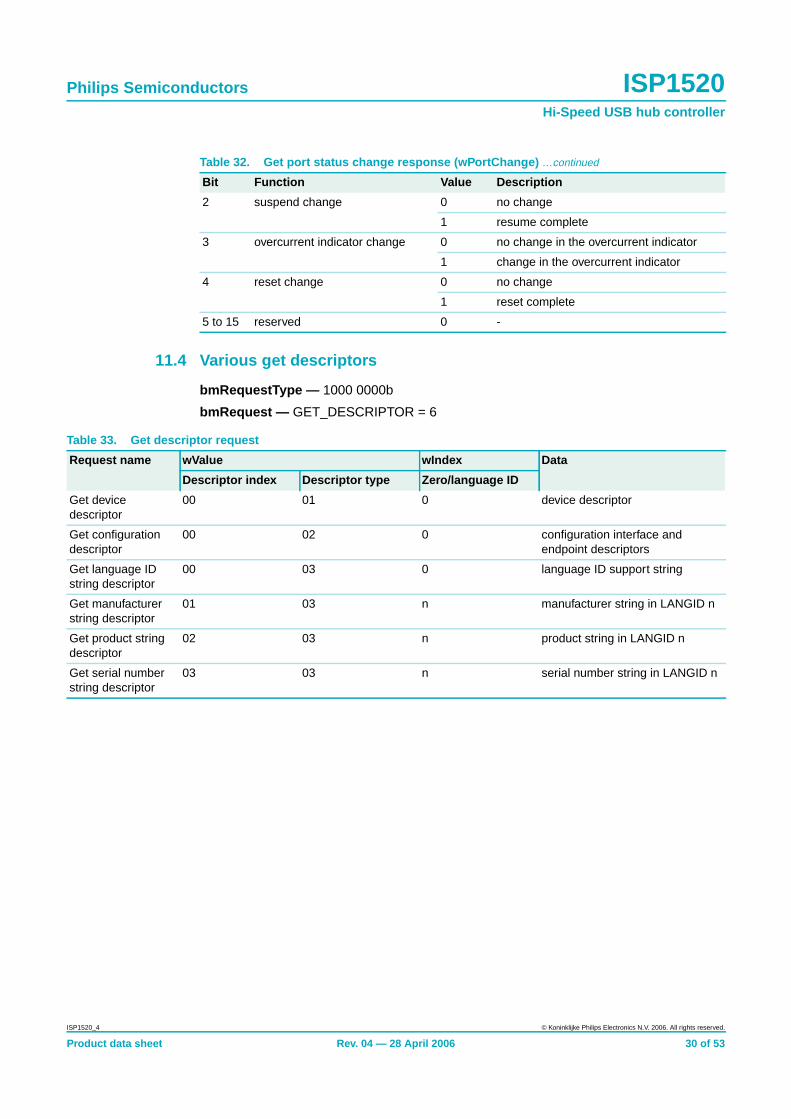
11.4 Various get descriptors
bmRequestType — 1000 0000b
bmRequest — GET_DESCRIPTOR = 6
2 suspend change 0 no change
1 resume complete
3 overcurrent indicator change 0 no change in the overcurrent indicator
1 change in the overcurrent indicator
4 reset change 0 no change
1 reset complete
5 to 15 reserved 0 -
Table 32. Get port status change response (wPortChange) …continued
Bit Function Value Description
Table 33. Get descriptor request
Request name wValue wIndex Data
Descriptor index Descriptor type Zero/language ID
Get devicedescriptor
00 01 0 device descriptor
Get configurationdescriptor
00 02 0 configuration interface andendpoint descriptors
Get language IDstring descriptor
00 03 0 language ID support string
Get manufacturerstring descriptor
01 03 n manufacturer string in LANGID n
Get product stringdescriptor
02 03 n product string in LANGID n
Get serial numberstring descriptor
03 03 n serial number string in LANGID n
ISP1520_4 © Koninklijke Philips Electronics N.V. 2006. All rights reserved.
Product data sheet Rev. 04 — 28 April 2006 30 of 53

Philips Semiconductors ISP1520Hi-Speed USB hub controller
12. Limiting values
[1] Valid only when supply voltage is present.
[2] Test method available on request.
[3] Equivalent to discharging a 100 pF capacitor through a 1.5 kΩ resistor (Human Body Model).
13. Recommended operating conditions
[1] All internal pull-up resistors are connected to this voltage.
[2] For full-speed operation, the temperature range can be extended up to +85 °C.
Table 34. Limiting valuesIn accordance with the Absolute Maximum Rating System (IEC 60134).
Symbol Parameter Conditions Min Max Unit
VCC(3V3) supply voltage (3.3 V) −0.5 +4.6 V
VREF(5V0) input reference voltage 5.0 V −0.5 +6.0 V
VI(5V0) input voltage on 5 V tolerant pins 3.0 V < VCC < 3.6 V [1] −0.5 +6.0 V
VI(3V3) 3.3 V input voltage 3.0 V < VCC < 3.6 V −0.5 +4.6 V
VO(3V3) output voltage on 3.3 V buffers −0.5 +4.6 V
Ilu latch-up current VI < 0 V or VI > VCC - 100 mA
Vesd electrostatic discharge voltage on pins DM1 to DM4, DP1 to DP4,OC1_N to OC4_N, and allVREF(5V0) and GND pins; ILI < 1 µA
[2][3] −4000 +4000 V
on all other pins; ILI < 1 µA [2][3] −2000 +2000 V
Tstg storage temperature −40 +125 °C
Table 35. Recommended operating conditions
Symbol Parameter Conditions Min Typ Max Unit
VCC(3V3) supply voltage (3.3 V) 3.0 3.3 3.6 V
VREF(5V0) input reference voltage 5.0 V [1] 4.5 5.0 5.5 V
VI(3V3) 3.3 V input voltage 0 - VCC V
VI(5V0) input voltage on 5 V tolerant pins 0 - VREF(5V0) V
Tamb ambient temperature −40 - +70[2] °C
ISP1520_4 © Koninklijke Philips Electronics N.V. 2006. All rights reserved.
Product data sheet Rev. 04 — 28 April 2006 31 of 53

Philips Semiconductors ISP1520Hi-Speed USB hub controller
14. Static characteristics
[1] Irrespective of the number of devices connected, the value of ICC is always 91 mA in full-speed.
[2] Total supply current for 3.3 V supply voltage.
[3] Including Rpu drop current.
[1] All pins are 5 V tolerant.
Table 36. Static characteristics: supply pinsVCC = 3.0 V to 3.6 V; Tamb = −40 °C to +70 °C; unless otherwise specified.
Symbol Parameter Conditions Min Typ Max Unit
Full-speed
IREF(5V0) supply current 5 V - 0.5 - mA
ICC(tot) total supply current ICC(tot) = ICC1 + ICC2 + ICC3 + ICC4[1][2] - 91 - mA
High-speed
ICC(tot) total supply current no device connected [2][3] - 136.3 - mA
one active device connected - 180 - mA
two active devices connected - 221 - mA
three active devices connected - 256 - mA
four active devices connected - 288 - mA
Table 37. Static characteristics: digital input and outputsVCC = 3.0 V to 3.6 V; Tamb = −40 °C to +70 °C; unless otherwise specified.[1]
Symbol Parameter Conditions Min Typ Max Unit
Digital input pins
VIL LOW-level input voltage - - 0.8 V
VIH HIGH-level input voltage 2.0 - - V
ILI input leakage current −1 - +1 µA
Schmitt-trigger input pins
Vth(LH) positive-going threshold voltage 1.4 - 1.9 V
Vth(HL) negative-going threshold voltage 0.9 - 1.5 V
Vhys hysteresis voltage 0.4 - 0.7 V
Overcurrent detection pins OC1_N to OC4_N
∆Vtrip overcurrent detection trip voltage ∆V = VCC − VOCn_N - 84 - mV
Digital output pins
VOL LOW-level output voltage - - 0.4 V
VOH HIGH-level output voltage 2.4 - - V
Open-drain output pins
IOZ off-state output current −1 - +1 µA
ISP1520_4 © Koninklijke Philips Electronics N.V. 2006. All rights reserved.
Product data sheet Rev. 04 — 28 April 2006 32 of 53
Philips Semiconductors ISP1520Hi-Speed USB hub controller
[1] All pins are 5 V tolerant.
[2] The bus capacitance (Cb) is specified in pF. To meet the specification for VOL and the maximum rise time (300 ns), use an externalpull-up resistor with Rmax = 850 / Cb kΩ and Rmin = (VCC − 0.4) / 3 kΩ.
[3] Output fall time VIH to VIL.
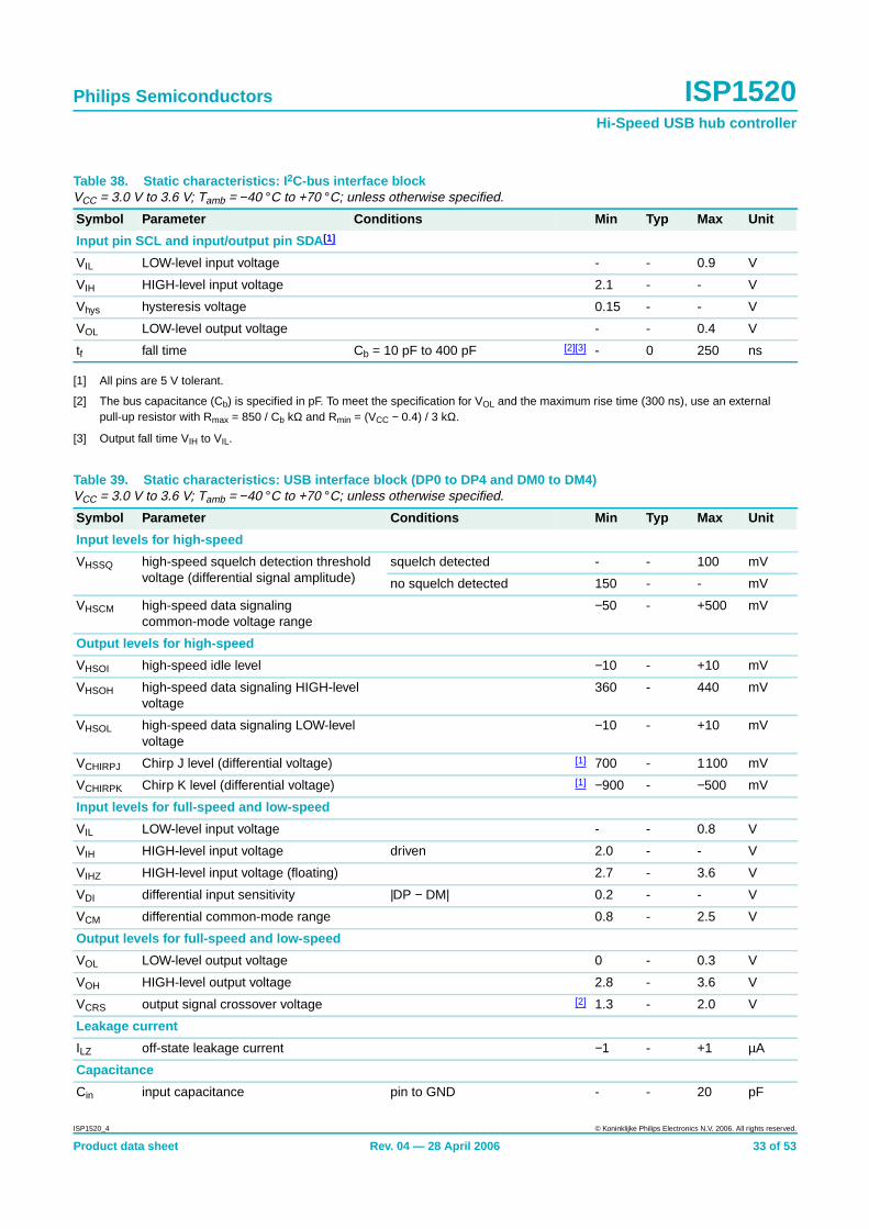
Table 38. Static characteristics: I 2C-bus interface blockVCC = 3.0 V to 3.6 V; Tamb = −40 °C to +70 °C; unless otherwise specified.
Symbol Parameter Conditions Min Typ Max Unit
Input pin SCL and input/output pin SDA [1]
VIL LOW-level input voltage - - 0.9 V
VIH HIGH-level input voltage 2.1 - - V
Vhys hysteresis voltage 0.15 - - V
VOL LOW-level output voltage - - 0.4 V
tf fall time Cb = 10 pF to 400 pF [2][3] - 0 250 ns
Table 39. Static characteristics: USB interface block (DP0 to DP4 and DM0 to DM4)VCC = 3.0 V to 3.6 V; Tamb = −40 °C to +70 °C; unless otherwise specified.
Symbol Parameter Conditions Min Typ Max Unit
Input levels for high-speed
VHSSQ high-speed squelch detection thresholdvoltage (differential signal amplitude)
squelch detected - - 100 mV
no squelch detected 150 - - mV
VHSCM high-speed data signalingcommon-mode voltage range
−50 - +500 mV
Output levels for high-speed
VHSOI high-speed idle level −10 - +10 mV
VHSOH high-speed data signaling HIGH-levelvoltage
360 - 440 mV
VHSOL high-speed data signaling LOW-levelvoltage
−10 - +10 mV
VCHIRPJ Chirp J level (differential voltage) [1] 700 - 1100 mV
VCHIRPK Chirp K level (differential voltage) [1] −900 - −500 mV
Input levels for full-speed and low-speed
VIL LOW-level input voltage - - 0.8 V
VIH HIGH-level input voltage driven 2.0 - - V
VIHZ HIGH-level input voltage (floating) 2.7 - 3.6 V
VDI differential input sensitivity |DP − DM| 0.2 - - V
VCM differential common-mode range 0.8 - 2.5 V
Output levels for full-speed and low-speed
VOL LOW-level output voltage 0 - 0.3 V
VOH HIGH-level output voltage 2.8 - 3.6 V
VCRS output signal crossover voltage [2] 1.3 - 2.0 V
Leakage current
ILZ off-state leakage current −1 - +1 µA
Capacitance
Cin input capacitance pin to GND - - 20 pF
ISP1520_4 © Koninklijke Philips Electronics N.V. 2006. All rights reserved.
Product data sheet Rev. 04 — 28 April 2006 33 of 53

Philips Semiconductors ISP1520Hi-Speed USB hub controller
[1] For minimum value, the HS termination resistor is disabled and the pull-up resistor is connected. Only during reset, when both the huband the device are capable of high-speed operation.
[2] Characterized only, not tested. Limits guaranteed by design.
Resistance
ZINP input impedance 10 - - MΩ
Termination
VTERM termination voltage for pull-up resistor on pinRPU
3.0 - 3.6 V
Table 39. Static characteristics: USB interface block (DP0 to DP4 and DM0 to DM4) …continuedVCC = 3.0 V to 3.6 V; Tamb = −40 °C to +70 °C; unless otherwise specified.
Symbol Parameter Conditions Min Typ Max Unit
ISP1520_4 © Koninklijke Philips Electronics N.V. 2006. All rights reserved.
Product data sheet Rev. 04 — 28 April 2006 34 of 53

Philips Semiconductors ISP1520Hi-Speed USB hub controller
15. Dynamic characteristics
[1] Recommended accuracy of the clock frequency is 500 ppm for the crystal.
[2] Suggested values for external capacitors when using a crystal are 22 pF to 27 pF.
[1] All pins are 5 V tolerant.
Table 40. Dynamic characteristics: system clock timing
Symbol Parameter Conditions Min Typ Max Unit
Reset
tW(POR) internal power-on reset pulsewidth
0.2 - 1 µs
tW(RESET_N) external RESET_N pulse width 0.2 - - µs
Crystal oscillator
fclk clock frequency crystal [1][2] - 12 - MHz
External clock input
δ clock duty cycle - 50 - %
Table 41. Dynamic characteristics: overcurrent sense timingVCC = 3.0 V to 3.6 V; Tamb = −40 °C to +70 °C; unless otherwise specified.
Symbol Parameter Conditions Min Typ Max Unit
Overcurrent sense pins OC1_N to OC4_N
ttrip overcurrent trip response time fromOCn_N LOW to PSWn_N HIGH
see Figure 9- - 15 ms
Overcurrent input: pins OCn_N; power switch output: pins PSWn_N.
Fig 9. Overcurrent trip response timing
mbl032
VCC
0 V
overcurrentinput
VCC
0 V
power switchoutput
ttrip
∆Vtrip
Table 42. Dynamic characteristics: digital pinsVCC = 3.0 V to 3.6 V; Tamb = −40 °C to +70 °C; unless otherwise specified.[1]
Symbol Parameter Conditions Min Typ Max Unit
tt(HL),tt(LH)
output transition time 4 - 15 ns
ISP1520_4 © Koninklijke Philips Electronics N.V. 2006. All rights reserved.
Product data sheet Rev. 04 — 28 April 2006 35 of 53

Philips Semiconductors ISP1520Hi-Speed USB hub controller
[1] Excluding the first transition from Idle state.
[2] Characterized only, not tested. Limits guaranteed by design.
Table 43. Dynamic characteristics: high-speed source electrical characteristicsVCC = 3.0 V to 3.6 V; Tamb = −40 °C to +70 °C; test circuit Figure 21; unless otherwise specified.
Symbol Parameter Conditions Min Typ Max Unit
Driver characteristics
tHSR rise time 10 % to 90 % 500 - - ps
tHSF fall time 90 % to 10 % 500 - - ps
Clock timing
tHSDRAT high-speed data rate 479.76 - 480.24 Mbit/s
tHSFRAM microframe interval 124.9375 - 125.0625 µs
tHSRFI consecutive microframe intervaldifference
1 - four high-speedbit times
ns
Table 44. Dynamic characteristics: full-speed source electrical characteristicsVCC = 3.0 V to 3.6 V; Tamb = −40 °C to +70 °C; test circuit Figure 22; unless otherwise specified.
Symbol Parameter Conditions Min Typ Max Unit
Driver characteristics
tFR rise time CL = 50 pF; 10 % to 90 % of|VOH − VOL|
4 - 20 ns
tFF fall time CL = 50 pF; 90 % to 10 % of|VOH − VOL|
4 - 20 ns
tFRFM differential rise and fall time matching [1] 90 - 111.1 %
VCRS output signal crossover voltage [1][2] 1.3 - 2.0 V
Data source timing [2]
tDJ1 source jitter total (including frequencytolerance) to next transition
see Figure 10 [1] −3.5 - +3.5 ns
tDJ2 source jitter total (including frequencytolerance) for paired transitions
see Figure 10 [1] −4 - +4 ns
tFEOPT source SE0 interval of EOP see Figure 11 160 - 175 ns
tFDEOP source jitter for differential transition toSE0 transition
see Figure 11 −2 - +5 ns
Receiver timing [2]
tJR1 receiver jitter to next transition see Figure 12 −18.5 - +18.5 ns
tJR2 receiver jitter for paired transitions see Figure 12 −9 - +9 ns
tFEOPR receiver SE0 interval of EOP accepted as EOP; seeFigure 11
82 - - ns
tFST width of SE0 interval during differentialtransition
rejected as EOP; seeFigure 13
- - 14 ns
Hub timing (downstream ports configured as full-speed) [2]
tFHDD hub differential data delay (without cable) see Figure 14; CL = 0 pF - - 44 ns
tFSOP data bit width distortion after SOP see Figure 14 −5 - +5 ns
tFEOPD hub EOP delay relative to tHDD see Figure 15 0 - 15 ns
tFHESK hub EOP output width skew see Figure 15 −15 - +15 ns
ISP1520_4 © Koninklijke Philips Electronics N.V. 2006. All rights reserved.
Product data sheet Rev. 04 — 28 April 2006 36 of 53

Philips Semiconductors ISP1520Hi-Speed USB hub controller
[1] Excluding the first transition from Idle state.
[2] Characterized only, not tested. Limits guaranteed by design.
Table 45. Dynamic characteristics: low-speed source electrical characteristicsVCC = 3.0 V to 3.6 V; Tamb = −40 °C to +70 °C; test circuit Figure 22; unless otherwise specified.
Symbol Parameter Conditions Min Typ Max Unit
Driver characteristics
tLR rise time 75 - 300 ns
tLF fall time 75 - 300 ns
tLRFM rise and fall time matching [1] 80 - 125 %
VCRS output signal crossover voltage [1][2] 1.3 - 2.0 V
Hub timing (downstream ports configured as full-speed)
tLHDD hub differential data delay see Figure 14 - - 300 ns
tLSOP data bit width distortion after SOP see Figure 14 [2] −60 - +60 ns
tLEOPD hub EOP delay relative to tHDD see Figure 15 [2] 0 - 200 ns
tLHESK hub EOP output width skew see Figure 15 [2] −300 - +300 ns
TPERIOD is the bit duration corresponding to the USB data rate.
Fig 10. Source differential data jitter
mgr870
TPERIOD
differentialdata lines
crossover point crossover point crossover point
consecutivetransitions
N × TPERIOD + tDJ1
pairedtransitions
N × TPERIOD + tDJ2
+3.3 V
0 V
TPERIOD is the bit duration corresponding to the USB data rate.
Full-speed timing symbols have a subscript prefix ‘F’, low-speed timing a prefix ‘L’.
Fig 11. Source differential data-to-EOP transition skew and EOP width
mgr776
TPERIOD
differentialdata lines
crossover point
differential data toSE0/EOP skew
N × TPERIOD + tDEOP
source EOP width: tEOPT
receiver EOP width: tEOPR
crossover pointextended
+3.3 V
0 V
ISP1520_4 © Koninklijke Philips Electronics N.V. 2006. All rights reserved.
Product data sheet Rev. 04 — 28 April 2006 37 of 53

Philips Semiconductors ISP1520Hi-Speed USB hub controller
TPERIOD is the bit duration corresponding to the USB data rate.
tJR is the jitter reference point.
Fig 12. Receiver differential data jitter
mgr871
TPERIOD
tJR
differentialdata lines
+3.3 V
0 VtJR1 tJR2
consecutivetransitions
N × TPERIOD + tJR1
pairedtransitions
N × TPERIOD + tJR2
Fig 13. Receiver SE0 width tolerance
mgr872
differentialdata lines
+3.3 V
0 V
tFST
VIH(min)
Full-speed timing symbols have a subscript prefix ‘F’, low-speed timing a prefix ‘L’.
Fig 14. Hub differential data delay and SOP distortion
mgr777
SOP distortion:tSOP = tHDD (next J) − tHDD(SOP)
(A) downstream hub delay (B) upstream hub delay
upstreamdifferentialdata lines
hub delaydownstream
tHDD
hub delayupstream
tHDD
downstreamdifferentialdata lines
downstreamdifferential
data
upstreamdifferential
data
crossoverpoint
crossoverpoint
crossoverpoint
crossoverpoint
+3.3 V
0 V
+3.3 V
0 V
ISP1520_4 © Koninklijke Philips Electronics N.V. 2006. All rights reserved.
Product data sheet Rev. 04 — 28 April 2006 38 of 53

Philips Semiconductors ISP1520Hi-Speed USB hub controller
Full-speed timing symbols have a subscript prefix ‘F’, low-speed timing a prefix ‘L’.
Fig 15. Hub EOP delay and EOP skew
mgr778
tEOP+tEOP− tEOP+tEOP−
crossoverpoint
extended
crossoverpoint
extended
EOP delay:tEOP = max (tEOP−, tEOP+)
EOP delay relative to tHDD:tEOPD = tEOP − tHDD
EOP skew:tHESK = tEOP+ − tEOP−
(A) downstream EOP delay (B) upstream EOP delay
upstreamdifferentialdata lines
downstreamport
crossoverpoint
extended
crossoverpoint
extended
upstreamend of cable
downstreamdifferentialdata lines
+3.3 V
0 V
+3.3 V
0 V
ISP1520_4 © Koninklijke Philips Electronics N.V. 2006. All rights reserved.
Product data sheet Rev. 04 — 28 April 2006 39 of 53

Philips Semiconductors ISP1520Hi-Speed USB hub controller
[1] fSCL = 1⁄64 × fXTAL.
[2] Rise time is determined by Cb and pull-up resistor value Rp (typical 4.7 kΩ).
[3] Setup time for (repeated) START condition.
[4] Hold time for (repeated) START condition.
[5] SCL LOW to data-out valid time.
Table 46. Dynamic characteristics: I 2C-bus (pins SDA and SCL)VCC and Tamb within recommended operating range; VDD = 5 V; VSS = VGND ; VIL and VIH between VSS and VDD.
Symbol Parameter Conditions Min Typ Max Unit
Clock frequency
fSCL SCL clock frequency fXTAL = 12 MHz [1] 0 93.75 100 kHz
General timing
t(SCL)L LOW period of the SCL clock 4.7 - - µs
t(SCL)H HIGH period of the SCL clock 4.0 - - µs
tr rise time SDA and SCL signals [2] - - 1000 ns
tf fall time SDA and SCL signals - - 300 ns
Cb capacitive load for each bus line - - 400 pF
SDA timing
tBUF bus free time between a STOP andSTART condition
4.7 - - µs
tSU;STA setup time for the START condition [3] 4.7 - - µs
tHD;STA hold time for the START condition [4] 4.0 - - µs
tSU;DAT data setup time 250 - - ns
tHD;DAT data hold time 0 - - µs
tSU;STO STOP condition setup time 4.0 - - µs
Additional I 2C-bus timing
tVD;DAT data valid time [5] - - 0.4 µs
Fig 16. I2C-bus timing
P S Sr P
004aaa814
tHD;STA
tBUF
tSU;STAtSU;DAT
tf
t(SCL)H t(SCL)L tSU;STO
tr
tHD;DAT
SDA
SCL
ISP1520_4 © Koninklijke Philips Electronics N.V. 2006. All rights reserved.
Product data sheet Rev. 04 — 28 April 2006 40 of 53

Philips Semiconductors ISP1520Hi-Speed USB hub controller
16. Application information
16.1 Descriptor configuration selection
16.2 Overcurrent detection limit adjustmentFor an overcurrent limit of 500 mA per port, a PMOS with RDSon of approximately 100 mΩis required. If a PMOS with a lower RDSon is used, analog overcurrent detection can beadjusted by using a series resistor; see Figure 18.
∆VPMOS = ∆Vtrip = ∆Vtrip(intrinsic) − (IOC(nom) × Radj(oc)), where:
∆VPMOS = voltage drop on PMOS
IOC(nom) = 0.6 µA.
The I2C-bus cannot be shared between the EEPROM and the external microcontroller; see Table 11.
(1) The function on port 4, which is a nonremovable port, is optional.
Fig 17. Descriptors configuration selection application diagram
004aaa303
ISP1520ROM
external microcontrolleracting as I2C-bus master
USB function
EEPROM
I2C-bus
four USB downstream facing ports
green andamber LEDs,
port 1
green andamber LEDs,
port 2
green andamber LEDs,
port 3
green andamber LEDs,
port 4(1)
upstream facing port GoodLink
(1) Radj(oc) is optional.
Fig 18. Adjusting analog overcurrent detection limit (optional)
004aaa259
VREF(5V0)
Radj(oc)(1)
5 V
ISP1520
OCn_NPSWn_N
IOC
ISP1520_4 © Koninklijke Philips Electronics N.V. 2006. All rights reserved.
Product data sheet Rev. 04 — 28 April 2006 41 of 53

Philips Semiconductors ISP1520Hi-Speed USB hub controller
16.3 Self-powered hub configurations
Fig 19. Self-powered hub; individual port power switching; individual overcurrent detection
PSW1_N
PSW2_N
TEST_HIGH
OC1_N
OC2_N
PSW4_N
OC4_N
5 V ± 3 %POWER SUPPLY−
+
1
VBUS
D+
D−GND
port 2to
port 3
SHIELD
+4.75 V(min)
+4.85 V (min)
VREF(5V0)
GND
ISP1520
120 µF
ferrite bead
downstreamport connector
T1
T4
0.1 µF
47 kΩ
004aaa305
3.3 V LDO VOLTAGE
REGULATOR
VCC
ADOC
4
VBUS
D+
D−GND
SHIELD
+4.75 V(min)120 µF
ferrite bead
0.1 µF
47 kΩ
TEST_LOW
PSW3_N
OC3_N
3.3 V or 5.0 V
ISP1520_4 © Koninklijke Philips Electronics N.V. 2006. All rights reserved.
Product data sheet Rev. 04 — 28 April 2006 42 of 53

Philips Semiconductors ISP1520Hi-Speed USB hub controller
Fig 20. Self-powered hub; ganged port power switching; global overcurrent detection
PSW1_N
TEST_HIGH
OC1_N
5.1 V ± 3 %POWER SUPPLY
(kick-up) −
+
1
VBUS
D+
D−GND
port 2to
port 3
SHIELD
+4.75 V(min)
+4.95 V (min)
VREF(5V0)
GND
ISP1520
120 µF
ferrite bead
downstreamport connector
T1
0.1 µF
47 kΩ
004aaa307
VCC
ADOC
4
VBUS
D+
D−GND
SHIELD
+4.75 V(min)120 µF
ferrite bead
low-ohmicsense resistorfor overcurrentdetection
OC2_N
OC3_N
OC4_N
+5 V
PSW3_N
PSW2_N
PSW4_NTEST_LOW
3.3 V LDO VOLTAGE
REGULATOR
3.3 V or 5.0 V
ISP1520_4 © Koninklijke Philips Electronics N.V. 2006. All rights reserved.
Product data sheet Rev. 04 — 28 April 2006 43 of 53

Philips Semiconductors ISP1520Hi-Speed USB hub controller
17. Test information
(1) Transmitter: connected to 50 Ω inputs of a high-speed differential oscilloscope.
Receiver: connected to 50 Ω outputs of a high-speed differential data generator.
Fig 21. High-speed transmitter and receiver test circuit
(1) CL = 50 pF for full-speed.
Fig 22. Full-speed test circuit
mdb273
DMn
DPn
50 Ω coax
50 Ω coax
DUT
GND
VCC
143 Ω
15.8 Ω
15.8 Ω
143 Ω
(1)
D−
D+
CL(1)
(1)
15 kΩ
DPn
DMn
RPU
3.3 V
1.5 kΩ ± 5%
DUT
mdb274
CL(1) 15 kΩ
test point
full-speed
test point
ISP1520_4 © Koninklijke Philips Electronics N.V. 2006. All rights reserved.
Product data sheet Rev. 04 — 28 April 2006 44 of 53

Philips Semiconductors ISP1520Hi-Speed USB hub controller
18. Package outline
Fig 23. LQFP64 package outline
UNITA
max. A1 A2 A3 bp c E(1) e HE L L p Zywv θ
REFERENCESOUTLINEVERSION
EUROPEANPROJECTION ISSUE DATE
IEC JEDEC JEITA
mm 1.6 0.200.05
1.451.35
0.250.270.17
0.180.12
10.19.9
0.512.1511.85
1.451.05
70
o
o0.12 0.11 0.2
DIMENSIONS (mm are the original dimensions)
Note
1. Plastic or metal protrusions of 0.25 mm maximum per side are not included.
0.750.45
SOT314-2 MS-026136E1000-01-1903-02-25
D(1) (1)(1)
10.19.9
HD
12.1511.85
EZ
1.451.05
D
bpe
θ
EA1
A
Lp
detail X
L
(A )3
B
16
c
DH
bp
EH A2
v M B
D
ZD
A
ZE
e
v M A
X
1
64
49
48 33
32
17
y
pin 1 index
w M
w M
0 2.5 5 mm
scale
LQFP64: plastic low profile quad flat package; 64 leads; body 10 x 10 x 1.4 mm SOT314-2
ISP1520_4 © Koninklijke Philips Electronics N.V. 2006. All rights reserved.
Product data sheet Rev. 04 — 28 April 2006 45 of 53

Philips Semiconductors ISP1520Hi-Speed USB hub controller
19. Soldering
19.1 Introduction to soldering surface mount packagesThis text gives a very brief insight to a complex technology. A more in-depth account ofsoldering ICs can be found in our Data Handbook IC26; Integrated Circuit Packages(document order number 9398 652 90011).
There is no soldering method that is ideal for all surface mount IC packages. Wavesoldering can still be used for certain surface mount ICs, but it is not suitable for fine pitchSMDs. In these situations reflow soldering is recommended.
19.2 Reflow solderingReflow soldering requires solder paste (a suspension of fine solder particles, flux andbinding agent) to be applied to the printed-circuit board by screen printing, stencilling orpressure-syringe dispensing before package placement. Driven by legislation andenvironmental forces the worldwide use of lead-free solder pastes is increasing.
Several methods exist for reflowing; for example, convection or convection/infraredheating in a conveyor type oven. Throughput times (preheating, soldering and cooling)vary between 100 seconds and 200 seconds depending on heating method.
Typical reflow peak temperatures range from 215 °C to 270 °C depending on solder pastematerial. The top-surface temperature of the packages should preferably be kept:
• below 225 °C (SnPb process) or below 245 °C (Pb-free process)
– for all BGA, HTSSON..T and SSOP..T packages
– for packages with a thickness ≥ 2.5 mm
– for packages with a thickness < 2.5 mm and a volume ≥ 350 mm3 so calledthick/large packages.
• below 240 °C (SnPb process) or below 260 °C (Pb-free process) for packages with athickness < 2.5 mm and a volume < 350 mm3 so called small/thin packages.
Moisture sensitivity precautions, as indicated on packing, must be respected at all times.
19.3 Wave solderingConventional single wave soldering is not recommended for surface mount devices(SMDs) or printed-circuit boards with a high component density, as solder bridging andnon-wetting can present major problems.
To overcome these problems the double-wave soldering method was specificallydeveloped.
If wave soldering is used the following conditions must be observed for optimal results:
• Use a double-wave soldering method comprising a turbulent wave with high upwardpressure followed by a smooth laminar wave.
• For packages with leads on two sides and a pitch (e):
– larger than or equal to 1.27 mm, the footprint longitudinal axis is preferred to beparallel to the transport direction of the printed-circuit board;
ISP1520_4 © Koninklijke Philips Electronics N.V. 2006. All rights reserved.
Product data sheet Rev. 04 — 28 April 2006 46 of 53

Philips Semiconductors ISP1520Hi-Speed USB hub controller
– smaller than 1.27 mm, the footprint longitudinal axis must be parallel to thetransport direction of the printed-circuit board.
The footprint must incorporate solder thieves at the downstream end.
• For packages with leads on four sides, the footprint must be placed at a 45° angle tothe transport direction of the printed-circuit board. The footprint must incorporatesolder thieves downstream and at the side corners.
During placement and before soldering, the package must be fixed with a droplet ofadhesive. The adhesive can be applied by screen printing, pin transfer or syringedispensing. The package can be soldered after the adhesive is cured.
Typical dwell time of the leads in the wave ranges from 3 seconds to 4 seconds at 250 °Cor 265 °C, depending on solder material applied, SnPb or Pb-free respectively.
A mildly-activated flux will eliminate the need for removal of corrosive residues in mostapplications.
19.4 Manual solderingFix the component by first soldering two diagonally-opposite end leads. Use a low voltage(24 V or less) soldering iron applied to the flat part of the lead. Contact time must belimited to 10 seconds at up to 300 °C.
When using a dedicated tool, all other leads can be soldered in one operation within2 seconds to 5 seconds between 270 °C and 320 °C.
19.5 Package related soldering information
[1] For more detailed information on the BGA packages refer to the (LF)BGA Application Note (AN01026);order a copy from your Philips Semiconductors sales office.
[2] All surface mount (SMD) packages are moisture sensitive. Depending upon the moisture content, themaximum temperature (with respect to time) and body size of the package, there is a risk that internal orexternal package cracks may occur due to vaporization of the moisture in them (the so called popcorneffect). For details, refer to the Drypack information in the Data Handbook IC26; Integrated CircuitPackages; Section: Packing Methods.
[3] These transparent plastic packages are extremely sensitive to reflow soldering conditions and must on noaccount be processed through more than one soldering cycle or subjected to infrared reflow soldering withpeak temperature exceeding 217 °C ± 10 °C measured in the atmosphere of the reflow oven. The packagebody peak temperature must be kept as low as possible.
Table 47. Suitability of surface mount IC packages for wave and reflow soldering methods
Package [1] Soldering method
Wave Reflow [2]
BGA, HTSSON..T[3], LBGA, LFBGA, SQFP,SSOP..T[3], TFBGA, VFBGA, XSON
not suitable suitable
DHVQFN, HBCC, HBGA, HLQFP, HSO, HSOP,HSQFP, HSSON, HTQFP, HTSSOP, HVQFN,HVSON, SMS
not suitable[4] suitable
PLCC[5], SO, SOJ suitable suitable
LQFP, QFP, TQFP not recommended[5][6] suitable
SSOP, TSSOP, VSO, VSSOP not recommended[7] suitable
CWQCCN..L[8], PMFP[9], WQCCN..L[8] not suitable not suitable
ISP1520_4 © Koninklijke Philips Electronics N.V. 2006. All rights reserved.
Product data sheet Rev. 04 — 28 April 2006 47 of 53

Philips Semiconductors ISP1520Hi-Speed USB hub controller
[4] These packages are not suitable for wave soldering. On versions with the heatsink on the bottom side, thesolder cannot penetrate between the printed-circuit board and the heatsink. On versions with the heatsinkon the top side, the solder might be deposited on the heatsink surface.
[5] If wave soldering is considered, then the package must be placed at a 45° angle to the solder wavedirection. The package footprint must incorporate solder thieves downstream and at the side corners.
[6] Wave soldering is suitable for LQFP, QFP and TQFP packages with a pitch (e) larger than 0.8 mm; it isdefinitely not suitable for packages with a pitch (e) equal to or smaller than 0.65 mm.
[7] Wave soldering is suitable for SSOP, TSSOP, VSO and VSSOP packages with a pitch (e) equal to or largerthan 0.65 mm; it is definitely not suitable for packages with a pitch (e) equal to or smaller than 0.5 mm.
[8] Image sensor packages in principle should not be soldered. They are mounted in sockets or deliveredpre-mounted on flex foil. However, the image sensor package can be mounted by the client on a flex foil byusing a hot bar soldering process. The appropriate soldering profile can be provided on request.
[9] Hot bar soldering or manual soldering is suitable for PMFP packages.
20. Abbreviations
21. References
[1] Universal Serial Bus Specification Rev. 2.0
[2] The I2C-bus specification
[3] ISP1520 Hub Demo Board User’s Guide
Table 48. Abbreviations
Acronym Description
ACPI Advanced Configuration and Power Interface
CRC Cyclical Redundancy Check
EEPROM Electronically Erasable Programmable Read-Only Memory
EMI ElectroMagnetic Interference
EOP End-of-Packet
ESD ElectroStatic Discharge
FET Field-Effect Transistor
HS High-Speed
LSB Least Significant Bit
MSB Most Significant Bit
MOSFET Metal Oxide Silicon Field Effect Transistor
NAK Not AcKnowledge
PCB Printed-Circuit Board
PID Packet IDentifier
PLL Phase-Locked Loop
SIE Serial Interface Engine
SOP Start-of-Packet
TT Transaction Translator
TTL Transistor-Transistor Logic
USB Universal Serial Bus
ISP1520_4 © Koninklijke Philips Electronics N.V. 2006. All rights reserved.
Product data sheet Rev. 04 — 28 April 2006 48 of 53

Philips Semiconductors ISP1520Hi-Speed USB hub controller
22. Revision history
Table 49. Revision history
Document ID Release date Data sheet status Change notice Supersedes
ISP1520_4 20060428 Product data sheet - ISP1520-03
Modifications: • The format of this data sheet has been redesigned to comply with the new presentation andinformation standard of Philips Semiconductors.
• Symbols and parameters have been changed, wherever applicable, to comply with the newpresentation and information standard of Philips Semiconductors.
• Section 2 “Features”: removed feature “USB suspend mode support”.
• Section 5 “Block diagram”: changed pin 1 from SUSPEND to TEST.
• Section 6 “Pinning information”:
– Changed pin 1 from SUSPEND to TEST, accordingly updated the I/O type and description.
– Updated description for the RESET_N pin.
– Removed the last sentence from the description for the HUBGL_N pin.
• Table 10 “I2C-bus slave address”: updated the last column.
• Table 35 “Recommended operating conditions”: added Table note [2].
• Table 36 “Static characteristics: supply pins”: removed the suspend mode current.
• Table 39 “Static characteristics: USB interface block (DP0 to DP4 and DM0 to DM4)”: removedtable note 3.
• Table 44 “Dynamic characteristics: full-speed source electrical characteristics”: removed the row ondriver output impedance ZDRV.
ISP1520-03(9397 750 13701)
20041124 Product data - ISP1520-02
ISP1520-02(9397 750 11689)
20040504 Product data - ISP1520-01
ISP1520-01(9397 750 10689)
20030625 Preliminary data - -
ISP1520_4 © Koninklijke Philips Electronics N.V. 2006. All rights reserved.
Product data sheet Rev. 04 — 28 April 2006 49 of 53

Philips Semiconductors ISP1520Hi-Speed USB hub controller
23. Legal information
23.1 Data sheet status
[1] Please consult the most recently issued document before initiating or completing a design.
[2] The term ‘short data sheet’ is explained in section “Definitions”.
[3] The product status of device(s) described in this document may have changed since this document was published and may differ in case of multiple devices. The latest product statusinformation is available on the Internet at URL http://www.semiconductors.philips.com.
23.2 Definitions
Draft — The document is a draft version only. The content is still underinternal review and subject to formal approval, which may result inmodifications or additions. Philips Semiconductors does not give anyrepresentations or warranties as to the accuracy or completeness ofinformation included herein and shall have no liability for the consequences ofuse of such information.
Short data sheet — A short data sheet is an extract from a full data sheetwith the same product type number(s) and title. A short data sheet is intendedfor quick reference only and should not be relied upon to contain detailed andfull information. For detailed and full information see the relevant full datasheet, which is available on request via the local Philips Semiconductorssales office. In case of any inconsistency or conflict with the short data sheet,the full data sheet shall prevail.
23.3 Disclaimers
General — Information in this document is believed to be accurate andreliable. However, Philips Semiconductors does not give any representationsor warranties, expressed or implied, as to the accuracy or completeness ofsuch information and shall have no liability for the consequences of use ofsuch information.
Right to make changes — Philips Semiconductors reserves the right tomake changes to information published in this document, including withoutlimitation specifications and product descriptions, at any time and withoutnotice. This document supersedes and replaces all information supplied priorto the publication hereof.
Suitability for use — Philips Semiconductors products are not designed,authorized or warranted to be suitable for use in medical, military, aircraft,space or life support equipment, nor in applications where failure ormalfunction of a Philips Semiconductors product can reasonably be expected
to result in personal injury, death or severe property or environmentaldamage. Philips Semiconductors accepts no liability for inclusion and/or useof Philips Semiconductors products in such equipment or applications andtherefore such inclusion and/or use is for the customer’s own risk.
Applications — Applications that are described herein for any of theseproducts are for illustrative purposes only. Philips Semiconductors makes norepresentation or warranty that such applications will be suitable for thespecified use without further testing or modification.
Limiting values — Stress above one or more limiting values (as defined inthe Absolute Maximum Ratings System of IEC 60134) may cause permanentdamage to the device. Limiting values are stress ratings only and operation ofthe device at these or any other conditions above those given in theCharacteristics sections of this document is not implied. Exposure to limitingvalues for extended periods may affect device reliability.
Terms and conditions of sale — Philips Semiconductors products are soldsubject to the general terms and conditions of commercial sale, as publishedat http://www.semiconductors.philips.com/profile/terms, including thosepertaining to warranty, intellectual property rights infringement and limitationof liability, unless explicitly otherwise agreed to in writing by PhilipsSemiconductors. In case of any inconsistency or conflict between informationin this document and such terms and conditions, the latter will prevail.
No offer to sell or license — Nothing in this document may be interpretedor construed as an offer to sell products that is open for acceptance or thegrant, conveyance or implication of any license under any copyrights, patentsor other industrial or intellectual property rights.
23.4 TrademarksNotice: All referenced brands, product names, service names and trademarksare the property of their respective owners.
GoodLink — is a trademark of Koninklijke Philips Electronics N.V.
I2C-bus — logo is a trademark of Koninklijke Philips Electronics N.V.
24. Contact information
For additional information, please visit: http://www.semiconductors.philips.com
For sales office addresses, send an email to: [email protected]
Document status [1] [2] Product status [3] Definition
Objective [short] data sheet Development This document contains data from the objective specification for product development.
Preliminary [short] data sheet Qualification This document contains data from the preliminary specification.
Product [short] data sheet Production This document contains the product specification.
ISP1520_4 © Koninklijke Philips Electronics N.V. 2006. All rights reserved.
Product data sheet Rev. 04 — 28 April 2006 50 of 53

Philips Semiconductors ISP1520Hi-Speed USB hub controller
25. Tables
Table 1. Ordering information . . . . . . . . . . . . . . . . . . . . .2Table 2. Pin description . . . . . . . . . . . . . . . . . . . . . . . . . .4Table 3. Configuration parameters . . . . . . . . . . . . . . . .11Table 4. Downstream facing port number pin
configuration . . . . . . . . . . . . . . . . . . . . . . . . . .12Table 5. Power switching mode: pin configuration . . . . .13Table 6. Overcurrent protection mode pin configuration 13Table 7. Overcurrent detection mode selection pin
configuration . . . . . . . . . . . . . . . . . . . . . . . . . .13Table 8. Nonremovable port pin configuration . . . . . . . .14Table 9. Port indicator support: pin configuration . . . . .14Table 10. I2C-bus slave address . . . . . . . . . . . . . . . . . . .15Table 11. Configuration method . . . . . . . . . . . . . . . . . . .16Table 12. ROM or EEPROM detailed map . . . . . . . . . . .16Table 13. Hub endpoints . . . . . . . . . . . . . . . . . . . . . . . . .21Table 14. Status Change byte: bit allocation . . . . . . . . . .22Table 15. Device descriptor . . . . . . . . . . . . . . . . . . . . . . .22Table 16. Device_qualifier descriptor . . . . . . . . . . . . . . .23Table 17. Other_speed_configuration descriptor . . . . . . .23Table 18. Configuration descriptor . . . . . . . . . . . . . . . . . .23Table 19. Interface descriptor . . . . . . . . . . . . . . . . . . . . .24Table 20. Endpoint descriptor . . . . . . . . . . . . . . . . . . . . .24Table 21. Hub descriptor . . . . . . . . . . . . . . . . . . . . . . . . .24Table 22. wHubCharacteristics bit description . . . . . . . .25Table 23. Standard USB requests . . . . . . . . . . . . . . . . . .25Table 24. Hub class requests . . . . . . . . . . . . . . . . . . . . .26Table 25. Hub class feature selector . . . . . . . . . . . . . . . .27Table 26. Get hub configuration response . . . . . . . . . . . .28Table 27. Get device status response . . . . . . . . . . . . . . .28Table 28. Get interface status response . . . . . . . . . . . . .28Table 29. Get endpoint status response . . . . . . . . . . . . .28Table 30. Get hub status response . . . . . . . . . . . . . . . . .28Table 31. Get port status response (wPortStatus) . . . . .29Table 32. Get port status change response
(wPortChange) . . . . . . . . . . . . . . . . . . . . . . . . .29Table 33. Get descriptor request . . . . . . . . . . . . . . . . . . .30Table 34. Limiting values . . . . . . . . . . . . . . . . . . . . . . . . .31Table 35. Recommended operating conditions . . . . . . . .31Table 36. Static characteristics: supply pins . . . . . . . . . .32Table 37. Static characteristics: digital input and
outputs . . . . . . . . . . . . . . . . . . . . . . . . . . . . . . .32Table 38. Static characteristics: I2C-bus interface block .33Table 39. Static characteristics: USB interface block
(DP0 to DP4 and DM0 to DM4) . . . . . . . . . . . .33Table 40. Dynamic characteristics: system clock timing .35Table 41. Dynamic characteristics: overcurrent sense
timing . . . . . . . . . . . . . . . . . . . . . . . . . . . . . . . .35Table 42. Dynamic characteristics: digital pins . . . . . . . .35
Table 43. Dynamic characteristics: high-speed sourceelectrical characteristics . . . . . . . . . . . . . . . . . 36
Table 44. Dynamic characteristics: full-speed sourceelectrical characteristics . . . . . . . . . . . . . . . . . 36
Table 45. Dynamic characteristics: low-speed sourceelectrical characteristics . . . . . . . . . . . . . . . . . 37
Table 46. Dynamic characteristics: I2C-bus(pins SDA and SCL) . . . . . . . . . . . . . . . . . . . . 40
Table 47. Suitability of surface mount IC packages forwave and reflow soldering methods . . . . . . . . 47
Table 48. Abbreviations . . . . . . . . . . . . . . . . . . . . . . . . . . 48Table 49. Revision history . . . . . . . . . . . . . . . . . . . . . . . . 49
ISP1520_4 © Koninklijke Philips Electronics N.V. 2006. All rights reserved.
Product data sheet Rev. 04 — 28 April 2006 51 of 53
continued >>

Philips Semiconductors ISP1520Hi-Speed USB hub controller
26. Figures
Fig 1. Block diagram . . . . . . . . . . . . . . . . . . . . . . . . . . . .3Fig 2. Pin configuration . . . . . . . . . . . . . . . . . . . . . . . . . .4Fig 3. Power-on reset timing . . . . . . . . . . . . . . . . . . . . .10Fig 4. External clock with respect to power-on reset . . .10Fig 5. Typical voltage drop components in self-powered
mode using individual overcurrent detection . . . .12Fig 6. Typical voltage drop components in self-powered
mode using global overcurrent detection . . . . . . .13Fig 7. Configurable hub descriptors . . . . . . . . . . . . . . . .15Fig 8. ROM or EEPROM map . . . . . . . . . . . . . . . . . . . .16Fig 9. Overcurrent trip response timing . . . . . . . . . . . . .35Fig 10. Source differential data jitter . . . . . . . . . . . . . . . .37Fig 11. Source differential data-to-EOP transition skew
and EOP width . . . . . . . . . . . . . . . . . . . . . . . . . . .37Fig 12. Receiver differential data jitter . . . . . . . . . . . . . . .38Fig 13. Receiver SE0 width tolerance . . . . . . . . . . . . . . .38Fig 14. Hub differential data delay and SOP distortion . .38Fig 15. Hub EOP delay and EOP skew . . . . . . . . . . . . . .39Fig 16. I2C-bus timing . . . . . . . . . . . . . . . . . . . . . . . . . . .40Fig 17. Descriptors configuration selection application
diagram . . . . . . . . . . . . . . . . . . . . . . . . . . . . . . . .41Fig 18. Adjusting analog overcurrent detection limit
(optional) . . . . . . . . . . . . . . . . . . . . . . . . . . . . . . .41Fig 19. Self-powered hub; individual port power
switching; individual overcurrent detection. . . . . .42Fig 20. Self-powered hub; ganged port power switching;
global overcurrent detection. . . . . . . . . . . . . . . . .43Fig 21. High-speed transmitter and receiver test circuit. .44Fig 22. Full-speed test circuit . . . . . . . . . . . . . . . . . . . . . .44Fig 23. LQFP64 package outline . . . . . . . . . . . . . . . . . . .45
ISP1520_4 © Koninklijke Philips Electronics N.V. 2006. All rights reserved.
Product data sheet Rev. 04 — 28 April 2006 52 of 53
continued >>

Philips Semiconductors ISP1520Hi-Speed USB hub controller
27. Contents
1 General description . . . . . . . . . . . . . . . . . . . . . . 12 Features . . . . . . . . . . . . . . . . . . . . . . . . . . . . . . . 23 Applications . . . . . . . . . . . . . . . . . . . . . . . . . . . . 24 Ordering information . . . . . . . . . . . . . . . . . . . . . 25 Block diagram . . . . . . . . . . . . . . . . . . . . . . . . . . 36 Pinning information . . . . . . . . . . . . . . . . . . . . . . 46.1 Pinning . . . . . . . . . . . . . . . . . . . . . . . . . . . . . . . 46.2 Pin description . . . . . . . . . . . . . . . . . . . . . . . . . 47 Functional description . . . . . . . . . . . . . . . . . . . 87.1 Analog transceivers . . . . . . . . . . . . . . . . . . . . . 87.2 Hub controller core . . . . . . . . . . . . . . . . . . . . . . 87.2.1 Philips serial interface engine . . . . . . . . . . . . . . 87.2.2 Routing logic . . . . . . . . . . . . . . . . . . . . . . . . . . . 87.2.3 Transaction translator . . . . . . . . . . . . . . . . . . . . 87.2.4 Mini-Host Controller . . . . . . . . . . . . . . . . . . . . . 87.2.5 Hub repeater. . . . . . . . . . . . . . . . . . . . . . . . . . . 97.2.6 Hub and port controllers . . . . . . . . . . . . . . . . . . 97.2.7 Bit clock recovery . . . . . . . . . . . . . . . . . . . . . . . 97.3 Phase-locked loop clock multiplier . . . . . . . . . . 97.4 I2C-bus controller . . . . . . . . . . . . . . . . . . . . . . . 97.5 Overcurrent detection circuit . . . . . . . . . . . . . . . 97.6 GoodLink . . . . . . . . . . . . . . . . . . . . . . . . . . . . . 97.7 Power-on reset . . . . . . . . . . . . . . . . . . . . . . . . . 98 Configuration selections. . . . . . . . . . . . . . . . . 118.1 Configuration through I/O pins . . . . . . . . . . . . 118.1.1 Number of downstream facing ports. . . . . . . . 118.1.2 Power switching . . . . . . . . . . . . . . . . . . . . . . . 128.1.2.1 Voltage drop requirements . . . . . . . . . . . . . . . 128.1.3 Overcurrent protection mode . . . . . . . . . . . . . 138.1.4 Nonremovable port . . . . . . . . . . . . . . . . . . . . . 148.1.5 Port indicator support . . . . . . . . . . . . . . . . . . . 148.2 Device descriptors and string descriptors
settings using I2C-bus. . . . . . . . . . . . . . . . . . . 148.2.1 Background information on I2C-bus . . . . . . . . 148.2.1.1 Different conditions on I2C-bus . . . . . . . . . . . . 148.2.1.2 Data transfer . . . . . . . . . . . . . . . . . . . . . . . . . . 158.2.1.3 I2C-bus address . . . . . . . . . . . . . . . . . . . . . . . 158.2.2 Architecture of configurable hub descriptors . 158.2.3 ROM or EEPROM map. . . . . . . . . . . . . . . . . . 168.2.4 ROM or EEPROM detailed map . . . . . . . . . . . 169 Hub controller description . . . . . . . . . . . . . . . 219.1 Endpoint 0. . . . . . . . . . . . . . . . . . . . . . . . . . . . 219.2 Endpoint 1. . . . . . . . . . . . . . . . . . . . . . . . . . . . 2110 Descriptors . . . . . . . . . . . . . . . . . . . . . . . . . . . . 2211 Hub requests . . . . . . . . . . . . . . . . . . . . . . . . . . 2511.1 Standard USB requests . . . . . . . . . . . . . . . . . 25
11.2 Hub class requests. . . . . . . . . . . . . . . . . . . . . 2611.3 Detailed responses to hub requests. . . . . . . . 2711.3.1 Get configuration . . . . . . . . . . . . . . . . . . . . . . 2711.3.2 Get device status . . . . . . . . . . . . . . . . . . . . . . 2811.3.3 Get interface status . . . . . . . . . . . . . . . . . . . . 2811.3.4 Get endpoint status . . . . . . . . . . . . . . . . . . . . 2811.3.5 Get hub status . . . . . . . . . . . . . . . . . . . . . . . . 2811.3.6 Get port status . . . . . . . . . . . . . . . . . . . . . . . . 2911.4 Various get descriptors. . . . . . . . . . . . . . . . . . 3012 Limiting values . . . . . . . . . . . . . . . . . . . . . . . . 3113 Recommended operating conditions . . . . . . 3114 Static characteristics . . . . . . . . . . . . . . . . . . . 3215 Dynamic characteristics . . . . . . . . . . . . . . . . . 3516 Application information . . . . . . . . . . . . . . . . . 4116.1 Descriptor configuration selection . . . . . . . . . 4116.2 Overcurrent detection limit adjustment. . . . . . 4116.3 Self-powered hub configurations . . . . . . . . . . 4217 Test information. . . . . . . . . . . . . . . . . . . . . . . . 4418 Package outline . . . . . . . . . . . . . . . . . . . . . . . . 4519 Soldering . . . . . . . . . . . . . . . . . . . . . . . . . . . . . 4619.1 Introduction to soldering surface mount
packages . . . . . . . . . . . . . . . . . . . . . . . . . . . . 4619.2 Reflow soldering. . . . . . . . . . . . . . . . . . . . . . . 4619.3 Wave soldering. . . . . . . . . . . . . . . . . . . . . . . . 4619.4 Manual soldering . . . . . . . . . . . . . . . . . . . . . . 4719.5 Package related soldering information . . . . . . 4720 Abbreviations . . . . . . . . . . . . . . . . . . . . . . . . . 4821 References . . . . . . . . . . . . . . . . . . . . . . . . . . . . 4822 Revision history . . . . . . . . . . . . . . . . . . . . . . . 4923 Legal information . . . . . . . . . . . . . . . . . . . . . . 5023.1 Data sheet status . . . . . . . . . . . . . . . . . . . . . . 5023.2 Definitions . . . . . . . . . . . . . . . . . . . . . . . . . . . 5023.3 Disclaimers. . . . . . . . . . . . . . . . . . . . . . . . . . . 5023.4 Trademarks . . . . . . . . . . . . . . . . . . . . . . . . . . 5024 Contact information . . . . . . . . . . . . . . . . . . . . 5025 Tables . . . . . . . . . . . . . . . . . . . . . . . . . . . . . . . . 5126 Figures . . . . . . . . . . . . . . . . . . . . . . . . . . . . . . . 5227 Contents. . . . . . . . . . . . . . . . . . . . . . . . . . . . . . 53
© Koninklijke Philips Electronics N.V. 2006. All rights reserved.For more information, please visit: http://www.semiconductors.philips.com.For sales office addresses, email to: [email protected].
Date of release: 28 April 2006
Document identifier: ISP1520_4
Please be aware that important notices concerning this document and the product(s)described herein, have been included in section ‘Legal information’.
Related Documents