Summary This applicaon note describes how to implement security- or safety-crical designs using the Xilinx ® Isolaon Design Flow (IDF) with the Xilinx Vivado ® Design Suite. Design applicaons include informaon assurance (single-chip cryptography), avionics, automove, and industrial applicaons. This document explains how to address the following objecves: • Implement isolated funcons in a Xilinx UltraScale+™ FPGA or a Zynq ® UltraScale+™ MPSoC • Verify the isolaon using the Xilinx Vivado Isolaon Verifier (VIV) You can purchase the Security Monitor IP core Product Brief developed by Xilinx to add addional security to your design. For more informaon, contact your local Xilinx ® representave to access these documents. This applicaon note specifically covers UltraScale+ FPGAs and Zynq UltraScale+ MPSoCs using Vivado Design Suite 2018.3, and builds on earlier IDF concepts. An example design is provided in the Isolaon Design Example for Zynq Ultrascale+ MPSoC Applicaon Note (XAPP1336). For more informaon, see Isolaon Design Example. Introduction The flexibility of programmable logic affords security-crical and safety-crical industries many advantages. However, before Isolaon Design Flow (IDF) was developed, in applicaons, such as informaon assurance, government contractors and agencies could not realize the full capability of programmable logic due to isolaon, reliability, and security concerns, and were therefore forced to use mulchip soluons. To address these concerns, the IDF was developed to allow independent funcons to operate on a single chip. Examples of single chip applicaons include, but are not limited to, redundant Type- I cryptographic modules, or resident safety- and non safety-crical funcons. The successful compleon of the Xilinx ® Isolaon Design Flow allows Xilinx to provide new technology for the informaon assurance (IA) industry, as well as, provide safety-crical funcons in avionics, automove, and industrial applicaons. Application Note: UltraScale+ Devices, Zynq UltraScale+ MPSoC Isolation Design Flow for UltraScale+ FPGAs and Zynq UltraScale+ MPSoCs XAPP1335 (v2.1) March 9, 2021 XAPP1335 (v2.1) March 9, 2021 www.xilinx.com Application Note 1

Welcome message from author
This document is posted to help you gain knowledge. Please leave a comment to let me know what you think about it! Share it to your friends and learn new things together.
Transcript

SummaryThis application note describes how to implement security- or safety-critical designs using theXilinx® Isolation Design Flow (IDF) with the Xilinx Vivado® Design Suite. Design applicationsinclude information assurance (single-chip cryptography), avionics, automotive, and industrialapplications. This document explains how to address the following objectives:
• Implement isolated functions in a Xilinx UltraScale+™ FPGA or a Zynq® UltraScale+™ MPSoC
• Verify the isolation using the Xilinx Vivado Isolation Verifier (VIV)
You can purchase the Security Monitor IP core Product Brief developed by Xilinx to addadditional security to your design. For more information, contact your local Xilinx®
representative to access these documents.
This application note specifically covers UltraScale+ FPGAs and Zynq UltraScale+ MPSoCs usingVivado Design Suite 2018.3, and builds on earlier IDF concepts.
An example design is provided in the Isolation Design Example for Zynq Ultrascale+ MPSoCApplication Note (XAPP1336). For more information, see Isolation Design Example.
IntroductionThe flexibility of programmable logic affords security-critical and safety-critical industries manyadvantages. However, before Isolation Design Flow (IDF) was developed, in applications, such asinformation assurance, government contractors and agencies could not realize the full capabilityof programmable logic due to isolation, reliability, and security concerns, and were thereforeforced to use multichip solutions.
To address these concerns, the IDF was developed to allow independent functions to operate ona single chip. Examples of single chip applications include, but are not limited to, redundant Type-I cryptographic modules, or resident safety- and non safety-critical functions.
The successful completion of the Xilinx® Isolation Design Flow allows Xilinx to provide newtechnology for the information assurance (IA) industry, as well as, provide safety-criticalfunctions in avionics, automotive, and industrial applications.
Application Note: UltraScale+ Devices, Zynq UltraScale+ MPSoC
Isolation Design Flow for UltraScale+FPGAs and Zynq UltraScale+ MPSoCs
XAPP1335 (v2.1) March 9, 2021
XAPP1335 (v2.1) March 9, 2021 www.xilinx.comApplication Note 1

Isolation Design FlowDeveloping a safe and secure single chip solution that contains multiple isolated functions in asingle FPGA is made possible through Xilinx® isolation technology. Special attributes, such asHD.ISOLATED and the features it enables, are necessary to provide controls to achieve theisolation needed to meet certifying agency requirements.
To better understand the details of the Isolation Design Flow (IDF), the designer needs to have asolid understanding of the hierarchical design flow, see Vivado Design Suite User Guide:Hierarchical Design (UG905). Many of the terms and processes in the partition flow are used inthe IDF. Areas that are different supersede the partition design flow and are identified in thisapplication note.
Common TerminologySome of the common terms used extensively in this document are ownership, function, logic,region, and fence. These terms are defined as follows:
• Ownership (physical/logical): The concept of physical versus logical ownership is an importantconcept to understand when using the IDF. This concept is described in detail in the section Concept of Ownership.
• Function: A collection of logic that performs a specific operation (for example, an AESencryptor).
• Logic: Circuits used to implement a specific function (e.g., flip-flop, look up table, and RAM).
• Isolated Region/Pblock: A physical construct used to restrict placement of logic to a specificregion of the device.
• Fence: The concept of physical versus logical ownership is an important concept comprised ofa set of unused tiles in which no routine or logic is present.
• Trusted Routing: The routes that satisfy the rules outlined in the following figures. Trustedrouting is automatically enabled after the HD.ISOLATED attribute is set to TRUE on at leastone isolated module. These routes are a subset of existing routing resources that meet thefollowing restrictions:
• No entry or exit point in the fence between isolated regions
• One source and one destination region
• Its entirety stays contained in the source/destination regions
• It does not come within one fence tile from another unintended isolation region
These rules act as a filter to all available routes in a given design. An example of routes thatwould be filtered are shown in the following figures. Example routes excluded forprogrammable interconnect points (PIPs), outside the intended isolation regions or proximityto unintended isolation regions, are also shown.
Isolation Design Flow for UltraScale+ FPGAs and Zynq UltraScale+ MPSoCs
XAPP1335 (v2.1) March 9, 2021 www.xilinx.comApplication Note 2Send Feedback

Figure 1: Trusted Routes within an Isolated Module
Figure 2: Trusted Routes between Isolated Modules
RulesA secure or safety-critical solution can be achieved while using FPGA design techniques andcoding styles with only moderate modifications to the development flow. Xilinx® Isolation DesignFlow (IDF) development requires the designer to consider floorplanning much earlier in thedesign process to ensure that proper isolation is achieved in logic, routing, and I/O buffers (IOBs).In addition to early floorplanning, the development flow is based on hierarchy. Each function thatis being isolated must be at its own level of hierarchy. Although this flow requires additionalsteps, the hierarchical approach has certain advantages.
There are a few unique design details that must be adhered to achieve an FPGA-based IDFsolution. Carefully consider all aspects of the design details explained in subsequent sections ofthis application note. These considerations include:
• Keep each function that is being isolated at its own level of hierarchy.
• Keep top level or non-isolated logic to a minimum. It is strongly encouraged to have onlyglobal clocks and resets at this level.
Isolation Design Flow for UltraScale+ FPGAs and Zynq UltraScale+ MPSoCs
XAPP1335 (v2.1) March 9, 2021 www.xilinx.comApplication Note 3Send Feedback
• Use a fence to separate isolated functions.
• IOBs must be instantiated inside isolated modules for proper isolation of the IOB. This can beachieved by manual user instantiation or automatically by the tools.
Note: Automatic logical inferencing by the tools is unique to the Vivado® Design Suite.
• On-chip communication between isolated functions is achieved through the use of trustedrouting (Tools automatically choose trusted routes along coincident physical borders).
Top Level LogicIsolated designs must keep the amount of top level logic to a minimum. In a typical IsolationDesign Flow (IDF) design, the only logic at the top level should be clock logic. Any componentthat is not part of an isolated module in the design hierarchy is optimized to the top level.Because isolation is defined by the HD.ISOLATED attribute being set on a hierarchical module, alltop logic is, by default, not isolated. This has the following implications:
• There are no placement constraints on top level logic other than it will not be placed in thefence.
○ Top level logic can be placed in any isolated Pblock.
• There are no routing restrictions on top level logic other than it will not violate the fence withused programmable interconnect points (PIPs).
○ Top level routes can route to, from, and through any isolated Pblock.
IMPORTANT! Vivado tools automatically take care of the placement of top logic. It ensures that top levellogic is not placed in the fence. If there is a large empty space in a design that is not encompassed by anyPblock, Vivado might place top logic in that empty space
Isolation PropertiesThe Vivado tool uses two specific properties to create an isolated design: HD.ISOLATED andHD.ISOLATED_EXEMPT.
The Vivado tool enables isolation of a specific function by the application of the HD.ISOLATEDproperty on the function. This property can be set either in the XDC file or the Vivado IntegratedDesign Environment (IDE).
The Tcl command is:
set_property HD.ISOLATED true [get_cells <function_hierarchical_path>/<function_instance_name>]
or
set_property HD.ISOLATED 1 [get_cells <function_hierarchical_path>/<function_instance_name>]
You can also set the property in the Vivado GUI. See Adding Property HD.ISOLATED under Elaboration for setting the property via Vivado IDE.
Isolation Design Flow for UltraScale+ FPGAs and Zynq UltraScale+ MPSoCs
XAPP1335 (v2.1) March 9, 2021 www.xilinx.comApplication Note 4Send Feedback

By default, when HD.ISOLATED is enabled on a function/module, all components and routingthat belong to that module are isolated. This means that unless it is communicating with anotherisolated module, all routing is contained within that module. This also means that all componentsof that module are placed in its corresponding isolated Pblock.
Note: You do not explicitly add any isolation property to a Pblock. When an isolated module having theproperty HD.ISOLATED set is mapped to a Pblock during the floorplanning stage, that Pblock becomes anisolated Pblock. For further details, see Mapping the Logical Ownership to the Physical Ownership.
When the HD.ISOLATED property is set on a module, global logic instantiated within that isolated modulecannot be routed globally because the module has been isolated. But, Vivado IDF allows you to instantiateglobal logic at any level. To support this and enable routing of the global logic, the propertyHD.ISOLATED_EXEMPT should be set on the global instances to override the default isolation behavior.By setting this property on the global logic instance, Vivado routes and treats it as global logic instead ofisolated logic.
The format to exempt a global logic instance from isolation is:
set_property HD.ISOLATED_EXEMPT true [get_cells <function_hierarchical_path>/<function_instance_name>]
or
set_property HD.ISOLATED_EXEMPT 1 [get_cells <function_hierarchical_path>/<function_instance_name>]
See Guidelines for Controlling Global Clocking Logic for more information regarding theHD.ISOLATED_EXEMPT property, including an example of setting HD.ISOLATED_EXEMPT onall global logic in the design.
Note: Only global logic can be at the top of an isolated design, but it can also be instantiated in an isolatedhierarchy if the HD.ISOLATED_EXEMPT property is used. By setting this property on global logic, theVivado tool effectively treats them as top level logic.
IMPORTANT! Every physical component in the FPGA including IOBs needed by an isolated module, mustbe owned by its corresponding isolated Pblock. The designer needs to create Pblocks in such a way that ithas all the resources needed by the corresponding isolated module. This implies that IOBs needed by anisolated module must also be included in the corresponding isolated Pblock. For details on floorplanning,see Floorplanning.
Isolation ModulesEach function/module requiring isolation must be in its own hierarchical block. The reason forthis is that each module that has the isolation attribute set has the attribute applied to thatmodule and its entire logical hierarchy (sub-modules under the parent module on whichHD.ISOLATED property is set).
Note: Nested isolated modules are not supported.
Isolation Design Flow for UltraScale+ FPGAs and Zynq UltraScale+ MPSoCs
XAPP1335 (v2.1) March 9, 2021 www.xilinx.comApplication Note 5Send Feedback

IDF has many additional constraint rules as opposed to traditional Partial Reconfiguration (PR), orhierarchical design flows from Vivado Design Suite User Guide: Hierarchical Design (UG905). It isnecessary to define one key attribute for each module to be isolated to invoke the IDF rules tocreate isolated designs. As discussed in the above section, this attribute is HD.ISOLATED andneeds to be set for each module that needs isolation for the backend Vivado implementationtools to use the IDF rules. This allows effective Floorplanning of an isolated design in IDF, andprotects redundant functions from undesired optimization.
Communication between Isolated ModulesWhen communication between isolated modules is required, there are two possible solutions:
• Trusted Routing is the preferred method. For details on the user rules, when using trustedrouting, refer to Trusted Routing Rules in the Design Guidance section. Trusted routing isautomatically taken care of by Vivado tools hence this is the preferred method.
• Signals can be taken off-chip from one isolated Pblock, routed through the PCB, and thenbrought back on-chip, in a separate isolated Pblock. Although possible, this method is notpreferred because it is complex and impractical.
Reference DesignFor clarity, an example single-chip 2 channel functional safety design is used throughout thisapplication note to describe the design details and tool flow. The following figure shows thefloorplan for the lab design as implemented in an XCZU5CG-SFVC784-1-e device. It consists offive isolated regions. In addition, this design has been implemented with Vivado® Design Suite2018.3, verified by the Vivado Isolation Verifier (VIV) 2.0, and provided to the designer as areference.
Figure 3: IDF Design Floorplan
Access the isolation design for this application note from Isolation Design Example for ZynqUltrascale+ MPSoC Application Note (XAPP1336).
Isolation Design Flow for UltraScale+ FPGAs and Zynq UltraScale+ MPSoCs
XAPP1335 (v2.1) March 9, 2021 www.xilinx.comApplication Note 6Send Feedback

Architecture OverviewMPSoC Chip LayoutXilinx® MPSoC devices are made up of several sections connected to each other. The processorsystem (PS) is a monolithic block which is connected to the programmable logic (PL) through a setof interconnect tiles. The PL is made up of columns of tiles organized into clock regions as shownin the following figure for the ZU5 architecture.
Figure 4: ZU5 Layout
Clock Regions and ColumnsEach MPSoC is built using similar architecture. The ZU5 programmable logic (PL) uses four rowsof three clock regions. Each clock region contains multiple columns of PL and dedicated block.Each column is composed of a single type of tiles. The number of tiles per column depends onthe height of the tile type. A column of configurable logic block (CLB) tiles has 60 tiles. The PCIe®
tile is an example of the tallest tile used. A column of PCIe has one tile.
The column width changes based on the tile type for that tile. It is important to understand thatthe column width for clock regions vertically arranged is constant. In other words, a column ofCLB tiles in the blue clock region extends to the same column in the red clock region below it allthe way to the last clock region going vertically down so the same width of the column ismaintained from clock region to clock region. See Figure 32: FPGA Layout for details.
Clock Spines and Interconnect ColumnsThe clock spine for each clock region is located in the center of each clock region as shown in thefollowing figure. The clocks are distributed vertically using the columns of interconnect tileswhich then drive local logic devices in other tiles. Refer to UltraScale Architecture ClockingResources User Guide (UG572) for more details on the UltraScale clock architecture.
Isolation Design Flow for UltraScale+ FPGAs and Zynq UltraScale+ MPSoCs
XAPP1335 (v2.1) March 9, 2021 www.xilinx.comApplication Note 7Send Feedback

Figure 5: Clock Spine Location
Interconnect tiles are used to route connections between logic tiles. These interconnect tiles arethe equivalent to route channels in ASIC designs, and also provide a convenient method toisolate logic regions.
Pblocks and Programmable UnitsA key difference between the UltraScale+ architecture and previous architectures supported byIDF is the use of back-to-back (B2B) interconnect tiles. Where previously one logic tile (CLE,BRAM, DSP, etc.) was associated with one or more dedicated interconnect tiles (INT column),UltraScale+ interconnect tiles service two distinct logic tiles (one on the left and one on the rightof the INT column). This group of tiles along with their shared interconnect is called aProgrammable Unit.
Thus, a Programmable Unit (PU) is a set of logical tiles such as CLEs, BRAMs, DSPs along withtheir shared interconnect tiles. For example, one Block RAM, five CLEs, and five interconnecttiles shared between the Block RAM and CLEs constitute one PU. For the sake of convenience,this can be called BRAM PU. Another instance of a PU can be a CLE and CLM tiles on either sideof a shared Interconnect (INT) tile. Example of PUs have been listed under Programmable UnitSizes.
You can think of a Pblock as a region in the FPGA which is made up of Programmable Units (PUs),while creating isolated designs. For IDF, a PU is the smallest logic building block that can beassigned to a Pblock. A Pblock is created by adding multiples PUs (as required) into it.
You must include the whole PU inside the Pblock while reserving resources during floorplanning.From the IDF perspective, having a part of the PU outside of the Pblock, for example, having aCLE tile of BRAM PU not included inside the Pblock renders the whole PU (in this case the wholeBRAM PU - BRAM, the interconnects, and the CLE tiles) unusable for the Vivado tools duringimplementation stage. This is deliberate in IDF design as all the tiles within a PU shareinterconnect (INT) tiles, and isolation tools cannot place logic in a tile unless the complete PU ofthat tile is in an isolated Pblock. To grab all the resources of a PU inside a Pblock, the snappingmode property of the Pblock must be set to FINE_GRAINED. See Derived Range and SnappingMode for detailed explanation.
Isolation Design Flow for UltraScale+ FPGAs and Zynq UltraScale+ MPSoCs
XAPP1335 (v2.1) March 9, 2021 www.xilinx.comApplication Note 8Send Feedback
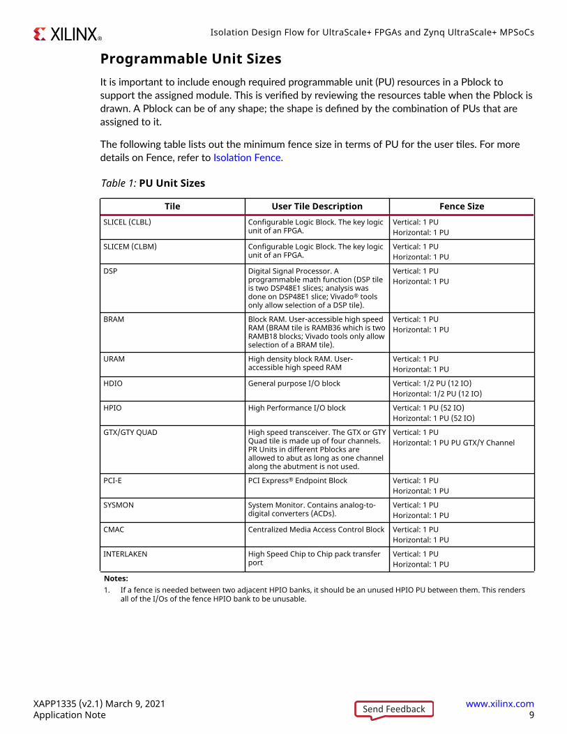
Programmable Unit SizesIt is important to include enough required programmable unit (PU) resources in a Pblock tosupport the assigned module. This is verified by reviewing the resources table when the Pblock isdrawn. A Pblock can be of any shape; the shape is defined by the combination of PUs that areassigned to it.
The following table lists out the minimum fence size in terms of PU for the user tiles. For moredetails on Fence, refer to Isolation Fence.
Table 1: PU Unit Sizes
Tile User Tile Description Fence SizeSLICEL (CLBL) Configurable Logic Block. The key logic
unit of an FPGA.Vertical: 1 PUHorizontal: 1 PU
SLICEM (CLBM) Configurable Logic Block. The key logicunit of an FPGA.
Vertical: 1 PUHorizontal: 1 PU
DSP Digital Signal Processor. Aprogrammable math function (DSP tileis two DSP48E1 slices; analysis wasdone on DSP48E1 slice; Vivado® toolsonly allow selection of a DSP tile).
Vertical: 1 PUHorizontal: 1 PU
BRAM Block RAM. User-accessible high speedRAM (BRAM tile is RAMB36 which is twoRAMB18 blocks; Vivado tools only allowselection of a BRAM tile).
Vertical: 1 PUHorizontal: 1 PU
URAM High density block RAM. User-accessible high speed RAM
Vertical: 1 PUHorizontal: 1 PU
HDIO General purpose I/O block Vertical: 1/2 PU (12 IO)Horizontal: 1/2 PU (12 IO)
HPIO High Performance I/O block Vertical: 1 PU (52 IO)Horizontal: 1 PU (52 IO)
GTX/GTY QUAD High speed transceiver. The GTX or GTYQuad tile is made up of four channels.PR Units in different Pblocks areallowed to abut as long as one channelalong the abutment is not used.
Vertical: 1 PUHorizontal: 1 PU PU GTX/Y Channel
PCI-E PCI Express® Endpoint Block Vertical: 1 PUHorizontal: 1 PU
SYSMON System Monitor. Contains analog-to-digital converters (ACDs).
Vertical: 1 PUHorizontal: 1 PU
CMAC Centralized Media Access Control Block Vertical: 1 PUHorizontal: 1 PU
INTERLAKEN High Speed Chip to Chip pack transferport
Vertical: 1 PUHorizontal: 1 PU
Notes:1. If a fence is needed between two adjacent HPIO banks, it should be an unused HPIO PU between them. This renders
all of the I/Os of the fence HPIO bank to be unusable.
Isolation Design Flow for UltraScale+ FPGAs and Zynq UltraScale+ MPSoCs
XAPP1335 (v2.1) March 9, 2021 www.xilinx.comApplication Note 9Send Feedback

Programmable Unit Size ExamplesThe smallest programmable unit (PU) is the CLB PU unit shown in the following figure. The CLBPU unit is 1/60th of a clock region high and two columns wide.
Figure 6: CLB PU
SLICE M INT SLICE L
X22162-010319
Isolation Design Flow for UltraScale+ FPGAs and Zynq UltraScale+ MPSoCs
XAPP1335 (v2.1) March 9, 2021 www.xilinx.comApplication Note 10Send Feedback

The next smallest programmable units are the DSP PU UNIT and the BRAM PU UNIT shown inthe following figures.
Figure 7: DSP PU
SLICE M INT
DSP
INTSLICE M
SLICE M
SLICE M
SLICE M
INT
INT
INT
X22163-010319
Figure 8: BRAM PU
BRAM 36
SLICE LINT
INT
INT
INT
INT
SLICE L
SLICE L
SLICE L
SLICE L
X22164-010319
Isolation Design Flow for UltraScale+ FPGAs and Zynq UltraScale+ MPSoCs
XAPP1335 (v2.1) March 9, 2021 www.xilinx.comApplication Note 11Send Feedback
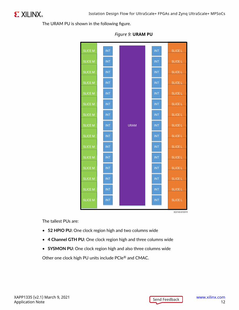
The URAM PU is shown in the following figure.
Figure 9: URAM PU
SLICE M
URAM
SLICE LINT
INT
INT
INT
INT
INT
INT
INT
INT
INT
INT
INT
INT
INT
INT
INT
INT
INT
INT
INT
INT
INT
INT
INT
INT
INT
INT
INT
INT
INT
SLICE M SLICE L
SLICE M
SLICE M
SLICE M
SLICE L
SLICE L
SLICE L
SLICE M
SLICE M
SLICE M
SLICE M
SLICE M
SLICE M
SLICE M
SLICE M
SLICE M
SLICE M
SLICE L
SLICE L
SLICE L
SLICE L
SLICE L
SLICE L
SLICE L
SLICE L
SLICE L
SLICE L
X22165-010319
The tallest PUs are:
• 52 HPIO PU: One clock region high and two columns wide
• 4 Channel GTH PU: One clock region high and three columns wide
• SYSMON PU: One clock region high and also three columns wide
Other one clock high PU units include PCIe® and CMAC.
Isolation Design Flow for UltraScale+ FPGAs and Zynq UltraScale+ MPSoCs
XAPP1335 (v2.1) March 9, 2021 www.xilinx.comApplication Note 12Send Feedback

Figure 10: HPIO PU
52 HPIO
INTSLICE L
INTSLICE L
INTSLICE L
SLICE L
SLICE LINT
INT
INTSLICE L
INTSLICE L
INTSLICE L
SLICE L
SLICE LINT
INT
INTSLICE L
INTSLICE L
INTSLICE L
SLICE L
SLICE LINT
INT
INTSLICE L
INTSLICE L
INTSLICE L
SLICE L
SLICE LINT
INT
INTSLICE L
INTSLICE L
INTSLICE L
SLICE L
SLICE LINT
INT
INTSLICE L
INTSLICE L
INTSLICE L
SLICE L
SLICE LINT
INT
INTSLICE L
INTSLICE L
INTSLICE L
SLICE L
SLICE LINT
INT
INTSLICE L
INT SLICE L
INT SLICE L
SLICE L
SLICE L
INT
INT
INT SLICE L
INT SLICE L
INT SLICE L
SLICE L
SLICE L
INT
INT
INT SLICE L
INT SLICE L
INT SLICE L
SLICE L
SLICE L
INT
INT
INT SLICE L
INT SLICE L
INT SLICE L
SLICE L
SLICE L
INT
INT
INT SLICE L
INT SLICE L
INT SLICE L
SLICE L
SLICE L
INT
INT
X22167-010319
Isolation Design Flow for UltraScale+ FPGAs and Zynq UltraScale+ MPSoCs
XAPP1335 (v2.1) March 9, 2021 www.xilinx.comApplication Note 13Send Feedback

Figure 11: GTH QUAD PU
INT
4 CHANNEL GTH
SLICE L
SLICE L
SLICE L
SLICE L
SLICE L
SLICE L
SLICE L
SLICE L
SLICE L
SLICE L
INT
SLICE L
SLICE L
SLICE L
SLICE L
SLICE L
SLICE L
SLICE L
SLICE L
SLICE L
SLICE L
SLICE L
SLICE L
SLICE L
SLICE L
SLICE L
SLICE L
SLICE L
SLICE L
SLICE L
SLICE L
SLICE L
SLICE L
SLICE L
SLICE L
SLICE L
SLICE L
SLICE L
SLICE L
SLICE L
SLICE L
SLICE L
SLICE L
SLICE L
SLICE L
SLICE L
SLICE L
SLICE L
SLICE L
SLICE L
SLICE L
SLICE L
SLICE L
SLICE L
SLICE L
SLICE L
SLICE L
SLICE L
SLICE L
SLICE L
SLICE L
INT
INT
INT
INT
INT
INT
INT
INT
INT
INT
INT
INT
INT
INT
INT
INT
INT
INT
INT
INT
INT
INT
INT
INT
INT
INT
INT
INT
INT
INT
INT
INT
INT
INT
INT
INT
INT
INT
INT
INT
INT
INT
INT
INT
INT
INT
INT
INT
INT
INT
INT
INT
INT
INT
INT
INT
INT
INT
X22168-010319
Isolation Design Flow for UltraScale+ FPGAs and Zynq UltraScale+ MPSoCs
XAPP1335 (v2.1) March 9, 2021 www.xilinx.comApplication Note 14Send Feedback
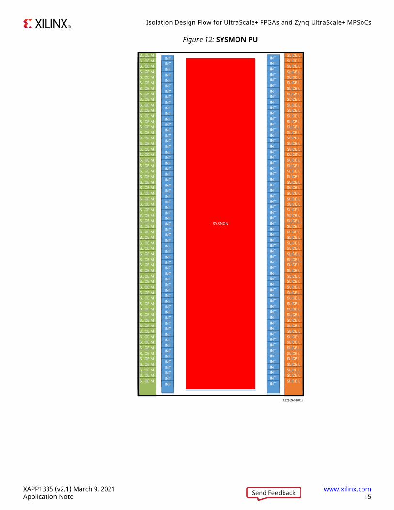
Figure 12: SYSMON PU
SLICE MINT
SYSMON
INTSLICE L
SLICE MSLICE MSLICE MSLICE M
SLICE LSLICE LSLICE LSLICE L
INTINTINTINT
INTINTINTINT
SLICE MINT INT
SLICE LSLICE MSLICE MSLICE MSLICE M
SLICE LSLICE LSLICE LSLICE L
INTINTINTINT
INTINTINTINT
SLICE MINT INT
SLICE LSLICE MSLICE MSLICE MSLICE M
SLICE LSLICE LSLICE LSLICE L
INTINTINTINT
INTINTINTINT
SLICE MINT INT
SLICE LSLICE MSLICE MSLICE MSLICE M
SLICE LSLICE LSLICE LSLICE L
INTINTINTINT
INTINTINTINT
SLICE MINT INT
SLICE LSLICE MSLICE MSLICE MSLICE M
SLICE LSLICE LSLICE LSLICE L
INTINTINTINT
INTINTINTINT
SLICE MINT INT
SLICE LSLICE MSLICE MSLICE MSLICE M
SLICE LSLICE LSLICE LSLICE L
INTINTINTINT
INTINTINTINT
SLICE MINT INT
SLICE LSLICE MSLICE MSLICE MSLICE M
SLICE LSLICE LSLICE LSLICE L
INTINTINTINT
INTINTINTINT
SLICE MINT INT
SLICE LSLICE MSLICE MSLICE MSLICE M
SLICE LSLICE LSLICE LSLICE L
INTINTINTINT
INTINTINTINT
SLICE MINT INT
SLICE LSLICE MSLICE MSLICE MSLICE M
SLICE LSLICE LSLICE LSLICE L
INTINTINTINT
INTINTINTINT
SLICE MINT INT
SLICE LSLICE MSLICE MSLICE MSLICE M
SLICE LSLICE LSLICE LSLICE L
INTINTINTINT
INTINTINTINT
SLICE MINT INT
SLICE LSLICE MSLICE MSLICE MSLICE M
SLICE LSLICE LSLICE LSLICE L
INTINTINTINT
INTINTINTINT
SLICE MINT INT
SLICE LSLICE MSLICE MSLICE MSLICE M
SLICE LSLICE LSLICE LSLICE L
INTINTINTINT
INTINTINTINT
X22169-010319
Isolation Design Flow for UltraScale+ FPGAs and Zynq UltraScale+ MPSoCs
XAPP1335 (v2.1) March 9, 2021 www.xilinx.comApplication Note 15Send Feedback

Figure 13: HDIO PU
SLICE MINT
HDIO
INTSLICE L
SLICE M
SLICE M
SLICE M
SLICE M
SLICE L
SLICE L
SLICE L
SLICE L
INT
INT
INT
INT
INT
INT
INT
INT
SLICE MINT INT
SLICE L
SLICE M
SLICE M
SLICE M
SLICE M
SLICE L
SLICE L
SLICE L
SLICE L
INT
INT
INT
INT
INT
INT
INT
INT
SLICE MINT INT
SLICE L
SLICE M
SLICE M
SLICE M
SLICE M
SLICE L
SLICE L
SLICE L
SLICE L
INT
INT
INT
INT
INT
INT
INT
INT
SLICE MINT INT
SLICE L
SLICE M
SLICE M
SLICE M
SLICE M
SLICE L
SLICE L
SLICE L
SLICE L
INT
INT
INT
INT
INT
INT
INT
INT
SLICE MINT INT
SLICE L
SLICE M
SLICE M
SLICE M
SLICE M
SLICE L
SLICE L
SLICE L
SLICE L
INT
INT
INT
INT
INT
INT
INT
INT
SLICE MINT INT
SLICE L
SLICE M
SLICE M
SLICE M
SLICE M
SLICE L
SLICE L
SLICE L
SLICE L
INT
INT
INT
INT
INT
INT
INT
INT
X22166-010319
Isolation Design Flow for UltraScale+ FPGAs and Zynq UltraScale+ MPSoCs
XAPP1335 (v2.1) March 9, 2021 www.xilinx.comApplication Note 16Send Feedback

Derived Range and Snapping ModeDerived range is the boundary of a Pblock after considering all the tiles of the Programable Units(PU) which are included in that specific Pblock. When the snapping mode property of a Pblock isset to OFF, then both derived range (calculated by internal tools), and XDC range (provided bythe user), compute the same Pblock boundary. But when the Snapping Mode property of aPblock is set to FINE_GRAINED, the derived range might differ from the user-specified XDCrange. This is because, if Snapping Mode property of a Pblock is set to FINE_GRAINED and ifsome of the tiles of a PU are left outside in the Pblock’s XDC range, then all the tiles in that PUare completely excluded from the Pblock boundary in the derived range computation.Understanding the concept of FINE_GRAINED SNAPPING_MODE is important as IDF onlyworks with this specific property.
In the following figure, the Pblock's snapping mode property is set to OFF, and all the tiles(irrespective of PU inclusion) are part of the Pblock. The only exceptions are the DSP and theBRAM tiles since entirety of these tiles is not inside the Pblock boundary. This can be verified bylooking at the blue shaded portion in the Pblock. The DSP and BRAM tiles are not part of thePblock because they are not highlighted; the whole tile needs to be included in the PBlock, andnot part of it. It can be observed in the following figure only one of the sites of the DSP andBRAM is included, and hence the tiles that are not highlighted got excluded in the derived rangecomputation.
Figure 14: A Pblock with SNAPPING_MODE Set to OFF
DSP Columns BRAM Column
X24355-081720
Isolation Design Flow for UltraScale+ FPGAs and Zynq UltraScale+ MPSoCs
XAPP1335 (v2.1) March 9, 2021 www.xilinx.comApplication Note 17Send Feedback

The following figure displays the same Pblock as the above figure but with the Pblock'sSNAPPING_MODE set to FINE_GRAINED. It can be observed that some of the tiles have beenexcluded (seen by the black regions inside blue shading) from the Pblock which were previouslyincluded when snapping mode was OFF. In the following figure, those specific tiles have beenexcluded whose PU is partially inside the Pblock. For example, in the portion of Pblock markedwith the red boxes, the CLEs got excluded because the DSP tiles and BRAM tile of the PU theyare part of, are not included in the Pblock boundary. Similarly, the CLEs surrounded by green boxare not included in the Pblock as they are part of a BRAM PU (the BRAM is towards the left andis not visible in the screen capture).
Note: In the following figure, the DSPs and BRAM inside the red box are not included as part of the Pblockin the first place because for a tile to be part of a Pblock (even with snapping mode OFF), the entirety ofthe tile must be inside the Pblock boundary. In this case, only one of the sites of the DSP and BRAM isinside of the Pblock boundary.
Figure 15: Pblock Shading with SNAPPING_MODE Set to FINE_GRAINED
DSP
DSP
CLEs
CLEs
CLEs
DSP
CLEs
BRAM
CLEs
X24356-081720
IMPORTANT! IDF works on derived range so ensure that Pblock’s SNAPPING_MODE property is set toFINE_GRAINED. This property can be set either in the Vivado GUI under Pblock property listed asSNAPPING_MODE, or via Tcl command as: set_property SNAPPING_MODE FINE_GRAINED[get_pblocks <Pblock_name>]
Note: The default value of SNAPPING_MODE property of isolated Pblocks is FINE_GRAINED.
Mapping the Logical Ownership to the Physical OwnershipOne of the most difficult concepts in IDF is the relationship between the logical ownership andthe physical ownership of a user design.
Isolation Design Flow for UltraScale+ FPGAs and Zynq UltraScale+ MPSoCs
XAPP1335 (v2.1) March 9, 2021 www.xilinx.comApplication Note 18Send Feedback

Logical Ownership refers to the actual Hardware Description Language (HDL) of the design.Physical Ownership refers to where that design resides in an FPGA, i.e., the actual placement ofthe HDL logics in the FPGA fabric. The mapping from the logical ownership to the physicalownership happens when a Pblock is created and a logical instance is assigned to it. This bindingof a logical instance or a portion of hierarchy, to a physical location in the device, is thefoundation of the Isolation Design Flow. This is achieved with the following commands:
create_pblock <Pblock_name>
add_cells_to_pblock [get_pblocks <Pblock_name>] [get_cells -quiet [list */<isolated_module_name>]]
After the Pblock has been created and logic has been assigned to it, the Pblock must be defined(floorplanned) to add the necessary resources as discussed in Floorplanning. Note that any FPGAphysical component - PU or routing resource that is not ranged / included in the Pblockdefinition cannot be used by the logic (module) assigned to that.
The following figure shows the logical ownership of four isolated modules – A, B, C, and D andthe global clock.
Figure 16: Logical View of the Four Isolated Modules
top_design.vhd
isomod_C.vhd isomod_D.vhd isomod_B.vhd isomod_A.vhd clock_gen.vhd
X24357-081720
The following figure shows the physical ownership for the four isolated modules of the previousfigure. The logical modules have been assigned Pblocks in the FPGA using Vivado tools with avalid fence between them.
Figure 17: Physical View of the Four Isolated Modules
Isolated Pblock B(isomod_B.vhd)
Isolated Pblock A(isomod_A.vhd)
Isolated Pblock C(isodmod_C.vhd)
Isolated Pblock D(isomod_D.vhd)
Fence
Fence
Fence Fence
MM
CM
BUFG
X24358-081720
Isolation Design Flow for UltraScale+ FPGAs and Zynq UltraScale+ MPSoCs
XAPP1335 (v2.1) March 9, 2021 www.xilinx.comApplication Note 19Send Feedback
IMPORTANT! Routing resources (interconnect tiles) associated with Pblock ranged components are addedautomatically by the tools. Interconnect tiles are not specifically defined in the Pblock definition (i.e., theXDC constraint file). When you add a PU to a Pblock, the associated corresponding interconnect tileresources are automatically added to the Pblock by Vivado tools.
Off-Chip Communication – Input / Output Buffer ControlIf an isolated module has inputs or outputs that must come from or go off-chip, these signalsmust have their IOBs inferred or instantiated inside an isolated module. While this is differentfrom standard FPGA design practice, it is required in order to have control over the routing of thesignals from the IOB to the function. If the IOB is not part of the isolated logic, there is no controlon how the signal is routed from the IOB to that isolated logic.
Note: If an isolated module's IOB is not instantiated inside the isolated module, Vivado will automaticallyattempt to move the IOB into the isolated module’s netlist. A more detailed description of Vivado toolsinsertion of IOBs is described in Hints and Guidelines under Automatic Movement of IOB into IsolatedHierarchy.
IMPORTANT! The general rule is that every physical component in the FPGA, including the IOBs, that isneeded by an isolated module must be owned by its corresponding isolated Pblock. It is the responsibilityof the designer to create Pblocks in such a way that it has all the resources needed by the correspondingisolated module. This implies that the IOBs needed by an isolated module must also be included in thecorresponding isolated Pblock. For details on floorplanning, see the Floorplanning section.
Isolation FenceTable 1 section lists out the fence sizes in terms of PUs for the various user tiles.
To achieve isolation within a single device, the concept of a fence is introduced. The fence is justa set of unused PUs in which no logic is present. The results of the isolation analysis performedby Xilinx shows that if specific PUs is placed between isolated Pblocks, it guarantees that nosingle point of failure exists that can compromise the isolation between the two Pblocks. Anexample of fence placement between two isolated modules is shown in the following Figure 18.In this figure, two Pblocks are defined (each outlined in purple and red). The translucent PUs arepart of the fence. The fence, like a Pblock, can be of any shape. The Vivado tools do not placeany logic in the fence PUs.
Isolation Design Flow for UltraScale+ FPGAs and Zynq UltraScale+ MPSoCs
XAPP1335 (v2.1) March 9, 2021 www.xilinx.comApplication Note 20Send Feedback
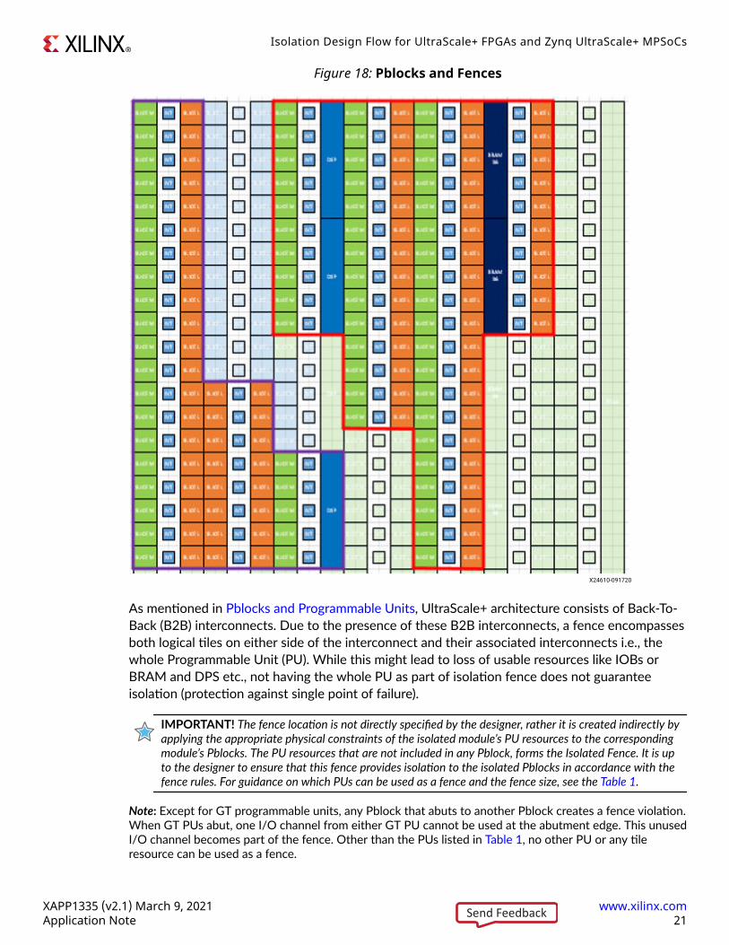
Figure 18: Pblocks and Fences
X24610-091720
As mentioned in Pblocks and Programmable Units, UltraScale+ architecture consists of Back-To-Back (B2B) interconnects. Due to the presence of these B2B interconnects, a fence encompassesboth logical tiles on either side of the interconnect and their associated interconnects i.e., thewhole Programmable Unit (PU). While this might lead to loss of usable resources like IOBs orBRAM and DPS etc., not having the whole PU as part of isolation fence does not guaranteeisolation (protection against single point of failure).
IMPORTANT! The fence location is not directly specified by the designer, rather it is created indirectly byapplying the appropriate physical constraints of the isolated module’s PU resources to the correspondingmodule’s Pblocks. The PU resources that are not included in any Pblock, forms the Isolated Fence. It is upto the designer to ensure that this fence provides isolation to the isolated Pblocks in accordance with thefence rules. For guidance on which PUs can be used as a fence and the fence size, see the Table 1.
Note: Except for GT programmable units, any Pblock that abuts to another Pblock creates a fence violation.When GT PUs abut, one I/O channel from either GT PU cannot be used at the abutment edge. This unusedI/O channel becomes part of the fence. Other than the PUs listed in Table 1, no other PU or any tileresource can be used as a fence.
Isolation Design Flow for UltraScale+ FPGAs and Zynq UltraScale+ MPSoCs
XAPP1335 (v2.1) March 9, 2021 www.xilinx.comApplication Note 21Send Feedback

The minimum fence width is determined by a detailed schematic analysis. This analysis providesfor a minimum of two faults (though in most cases it is much more) before the separationbetween two isolated modules is violated. While it is not mandatory to keep the size of the fenceto this minimum as listed in Table 1, you can incur a stiff penalty for using larger fences. Since IDFrules prevent routing touchdowns in the fence (i.e., having a PIP in the fence), having a fence sizelarger than the minimum does not provide any more protection against faults but rather mightlead to difficulty in meeting routing and timing constraints.
There are Trusted Routing rules that act as a filter to the router when implementing isolateddesigns (see Trusted Routing Rules). Any route that violates the Trusted Routing rules getsremoved from the list of valid resources visible to the router. This is what creates the trustedroutes – i.e., all possible routes that adheres to the rules such as no touchdown in fence, no PIPsin fence, and so on. If the fence in the design is too wide, all routes are removed and then thedesign will not be able to route (if communication across that boundary is intended). Hence, it ishighly recommended to keep the minimum size fence width to maximize the routing resourcesavailable between isolated Pblocks. Additionally, if two isolated modules communicate with eachother, then their corresponding Pblocks must be adjacent, i.e., side by side, along with a validfence between them. It can give rise to issues if this is not the case.
Fence Around Processor Subsystem for Zynq UltraScale+DevicesIn Zynq UltraScale+ devices, there is a PSS Programmable Unit. This PU consists of thePSS_ALTO Tile, Interconnects, and a column of CLEs as high as the PSS tile. The following figureshows the PSS PU:
Isolation Design Flow for UltraScale+ FPGAs and Zynq UltraScale+ MPSoCs
XAPP1335 (v2.1) March 9, 2021 www.xilinx.comApplication Note 22Send Feedback
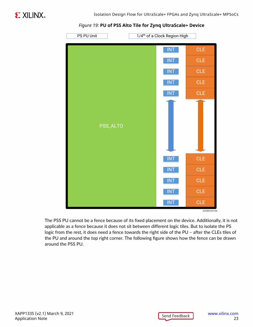
Figure 19: PU of PSS Alto Tile for Zynq UltraScale+ Device
PS PU Unit 1/4th of a Clock Region High
PSS_ALTO
CLE
CLE
INT
INT
INT
INT
INT
INT
INT
INT
INT
INT
CLE
CLE
CLE
CLE
CLE
CLE
CLE
CLE
X24589-091320
The PSS PU cannot be a fence because of its fixed placement on the device. Additionally, it is notapplicable as a fence because it does not sit between different logic tiles. But to isolate the PSlogic from the rest, it does need a fence towards the right side of the PU – after the CLEs tiles ofthe PU and around the top right corner. The following figure shows how the fence can be drawnaround the PSS PU.
Isolation Design Flow for UltraScale+ FPGAs and Zynq UltraScale+ MPSoCs
XAPP1335 (v2.1) March 9, 2021 www.xilinx.comApplication Note 23Send Feedback
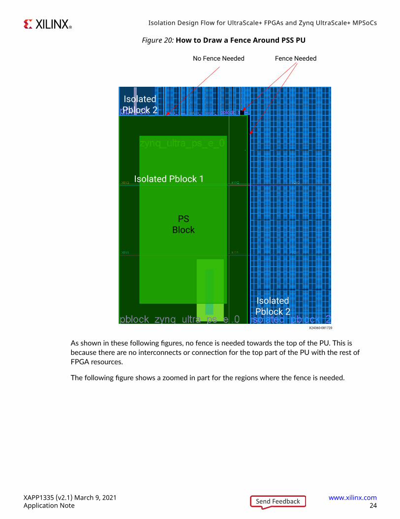
Figure 20: How to Draw a Fence Around PSS PU
PS Block
Isolated Pblock 2
Isolated Pblock 2
Isolated Pblock 1
No Fence Needed Fence Needed
X24360-081720
As shown in these following figures, no fence is needed towards the top of the PU. This isbecause there are no interconnects or connection for the top part of the PU with the rest ofFPGA resources.
The following figure shows a zoomed in part for the regions where the fence is needed.
Isolation Design Flow for UltraScale+ FPGAs and Zynq UltraScale+ MPSoCs
XAPP1335 (v2.1) March 9, 2021 www.xilinx.comApplication Note 24Send Feedback

Figure 21: Zoomed in Image for Top-Right Part of the PSS PU
So, to isolate the PSS isolated Pblock (shown here in green color) with another adjacent isolatedPblock (shown here in blue color), you will need one column PU fence towards the right of thePSS PU, from top to bottom. In Figure 20: PU of PSS Alto tile for Zynq UltraScale+ Device, CLBPUs (the next available PU after the PSS PU) has been used as fence starting from the top of thePSS PU to the bottom (entire right side), of the PSS PU. The previous figure shows a zoomed inpart of the same. Additionally, a fence comprising of 3 PUs is needed towards the top right toaccount for adjacency violation between the PSS Pblock (green) and the adjacent Pblock (blue).One PU fence is directly on top of the CLEs of the PSS PU. The other two PU fences are on theleft and right sides. In the previous figure, the middle fence is made of a CLB PU, the left of it is aDSP PU, and the right of it is a CLB PU.
Note: The above screen captures are just for reference. The actual PUs for the fences might differ from partto part, e.g., instead of the DSP PU, the top left fence can be a CLB PU. However, you need to ensure thatthere is fence towards the whole right columns, as well as top right corner of the PSS PU (if used as part ofisolation design). In smaller Zynq UltraScale+ devices there might not be any user tiles on top of the PSSPU, the whole left side of the part is the PSS PU. In that case, you may need a fence only towards the rightcolumn of the PSS PU (and not the top corner).
Fence for SSIT DevicesIn case of SSIT Devices, the SLR boundaries serve as natural isolation boundary/fence. Noadditional fence is required between SLRs if a SLR region contains only one isolated Pblock. Ifevery SLR region consists of a single isolated Pblock, no additional fence is needed. However, if aSLR region contains multiple isolated Pblocks, the appropriate fence is needed between them
The following figure shows (four) 4 isolated Pblocks, highlighted in (four) 4 different colors, drawnin each SLR regions of an SSIT device. No explicit fence is needed between the Pblocks as theSLR boundaries serve as isolation fence.
Isolation Design Flow for UltraScale+ FPGAs and Zynq UltraScale+ MPSoCs
XAPP1335 (v2.1) March 9, 2021 www.xilinx.comApplication Note 25Send Feedback
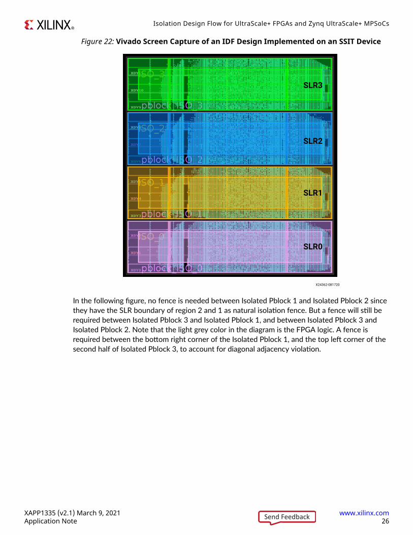
Figure 22: Vivado Screen Capture of an IDF Design Implemented on an SSIT Device
SLR3
SLR2
SLR1
SLR0
X24362-081720
In the following figure, no fence is needed between Isolated Pblock 1 and Isolated Pblock 2 sincethey have the SLR boundary of region 2 and 1 as natural isolation fence. But a fence will still berequired between Isolated Pblock 3 and Isolated Pblock 1, and between Isolated Pblock 3 andIsolated Pblock 2. Note that the light grey color in the diagram is the FPGA logic. A fence isrequired between the bottom right corner of the Isolated Pblock 1, and the top left corner of thesecond half of Isolated Pblock 3, to account for diagonal adjacency violation.
Isolation Design Flow for UltraScale+ FPGAs and Zynq UltraScale+ MPSoCs
XAPP1335 (v2.1) March 9, 2021 www.xilinx.comApplication Note 26Send Feedback
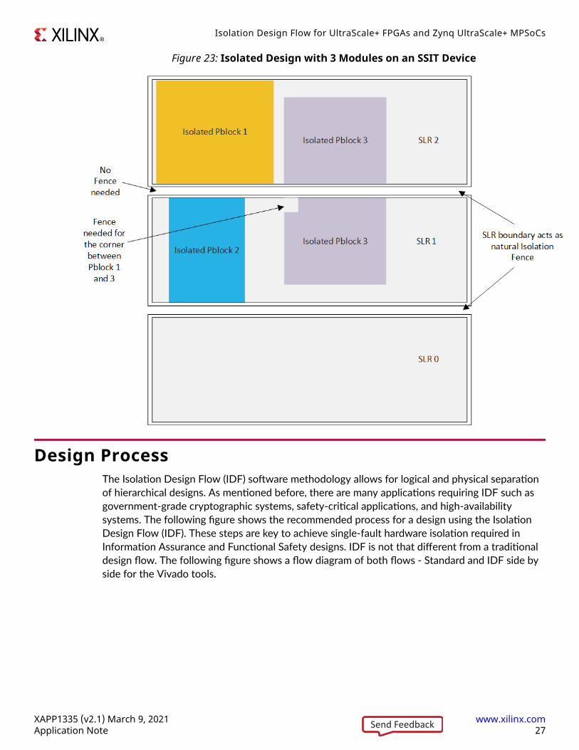
Figure 23: Isolated Design with 3 Modules on an SSIT Device
Design ProcessThe Isolation Design Flow (IDF) software methodology allows for logical and physical separationof hierarchical designs. As mentioned before, there are many applications requiring IDF such asgovernment-grade cryptographic systems, safety-critical applications, and high-availabilitysystems. The following figure shows the recommended process for a design using the IsolationDesign Flow (IDF). These steps are key to achieve single-fault hardware isolation required inInformation Assurance and Functional Safety designs. IDF is not that different from a traditionaldesign flow. The following figure shows a flow diagram of both flows - Standard and IDF side byside for the Vivado tools.
Isolation Design Flow for UltraScale+ FPGAs and Zynq UltraScale+ MPSoCs
XAPP1335 (v2.1) March 9, 2021 www.xilinx.comApplication Note 27Send Feedback

Figure 24: Design Flow Chart for IDF
Design CaptureThe is where the design may be captured in the Vivado® Design Suite. As shown in Figure 24,instead of using the IP integrator, Verilog, or VHDL code can also be used for creating theisolated modules. After the design is captured, a functional hierarchy is established, based onyour isolation strategy with respect to how data is flowing in your design. These create thelogical boundaries which will define the physical isolation as the design flow is implemented. Thisstep is critical as all other activities are based on this hierarchy.
The isolated modules require an additional wrapper after the hierarchy gets established. Thesemodules are captured via an IP integrator. This additional wrapper is required to enable portsplitting that might not be allowed by tool generated items, such as the hierarchy created by thetriple modular redundancy (TMR) management tool. See Isolation Design Example for ZynqUltrascale+ MPSoC Application Note (XAPP1336) for further details.
Figure 25: IP Integrator Tool Generated Design Example
Isolation Design Flow for UltraScale+ FPGAs and Zynq UltraScale+ MPSoCs
XAPP1335 (v2.1) March 9, 2021 www.xilinx.comApplication Note 28Send Feedback
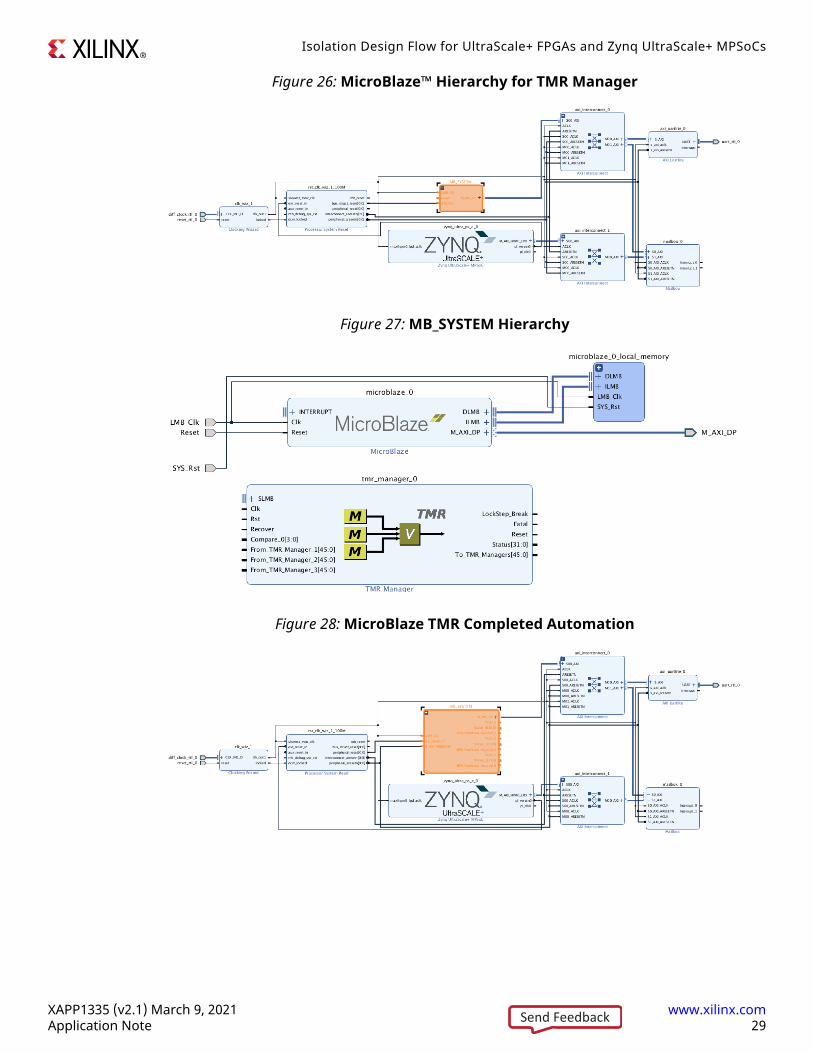
Figure 26: MicroBlaze™ Hierarchy for TMR Manager
Figure 27: MB_SYSTEM Hierarchy
Figure 28: MicroBlaze TMR Completed Automation
Isolation Design Flow for UltraScale+ FPGAs and Zynq UltraScale+ MPSoCs
XAPP1335 (v2.1) March 9, 2021 www.xilinx.comApplication Note 29Send Feedback

Figure 29: Updated MB_SYSTEM Hiearchy with TMR Implemented
Figure 30: MB_SYSTEM Hierarchy Removed to Flatten Design for Wrappers
Figure 31: 5 User-Created Hierarchy (Wrappers)
SimulationThis step verifies functional expectation of your design. There are no additional actions requiredto comply with the isolation design flow (IDF).
Isolation Design Flow for UltraScale+ FPGAs and Zynq UltraScale+ MPSoCs
XAPP1335 (v2.1) March 9, 2021 www.xilinx.comApplication Note 30Send Feedback

ElaborationIn Isolation Design Flow (IDF), the HD.ISOLATED property is added and enabled for each user-created wrappers that need to be isolated from each other. All other modules that do not requireisolation do not get this property added. Such modules will get optimized to top level and haveno place and route restrictions beyond keeping the fence intact. At this point in the design flow,this property is added on each wrapper, so synthesis knows which hierarchy is isolated,preventing optimization across isolation boundaries.
Figure 32: Adding Property HD.ISOLATED
Isolation Design Flow for UltraScale+ FPGAs and Zynq UltraScale+ MPSoCs
XAPP1335 (v2.1) March 9, 2021 www.xilinx.comApplication Note 31Send Feedback
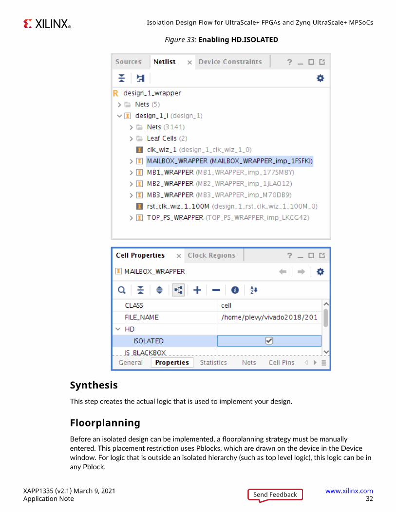
Figure 33: Enabling HD.ISOLATED
SynthesisThis step creates the actual logic that is used to implement your design.
FloorplanningBefore an isolated design can be implemented, a floorplanning strategy must be manuallyentered. This placement restriction uses Pblocks, which are drawn on the device in the Devicewindow. For logic that is outside an isolated hierarchy (such as top level logic), this logic can be inany Pblock.
Isolation Design Flow for UltraScale+ FPGAs and Zynq UltraScale+ MPSoCs
XAPP1335 (v2.1) March 9, 2021 www.xilinx.comApplication Note 32Send Feedback

FPGA arrays are made up of multiple clock regions with columns of logic resources within eachclock region. Each logic resource has a fixed height which are stacked one on top of another tomake up a column as shown in the following figure. Pblocks span these regions, but if a resource,such as a PCI™ block, which takes an entire clock region, is not enclosed by a single Pblock, it willnot be included in the Pblock. Before creating each Pblock, map out where each Pblock will belocated.
Figure 34: FPGA Layout
Isolation Design Flow for UltraScale+ FPGAs and Zynq UltraScale+ MPSoCs
XAPP1335 (v2.1) March 9, 2021 www.xilinx.comApplication Note 33Send Feedback

Drawing Pblocks Using Vivado GUIFloorplanning is accomplished by using Pblocks. Drawing Pblocks is a multi-step process which isoutlined here. This is the recommended process, but not the only method. See Drawing PblocksUsing Tcl Commands.
On a synthesized design:
1. In the NETLIST window, right-click a module to be isolated. For this example, select awrapper entry under design_1_i.
2. Select Floorplanning → Draw Pblock as shown in the following figure.
3. In the Device window, draw a rectangle that defines the initial Pblock as shown in thefollowing figure.
Isolation Design Flow for UltraScale+ FPGAs and Zynq UltraScale+ MPSoCs
XAPP1335 (v2.1) March 9, 2021 www.xilinx.comApplication Note 34Send Feedback

Once a Pblock is created, the Statistics window in Pblock Properties is updated, whichoutlines the percentage the Pblock resources that satisfies the synthesized requirements ofthe isolated region hierarchy as shown in the following figure.
4. To add more resources to a Pblock, in the Device window, select the Pblock to highlight theregion.
5. Right-click the highlighted region, and select Add Pblock Rectangle. As you grow the size ofthe Pblock, the Statistics window will update showing added resources. Pblocks can be anyshape.
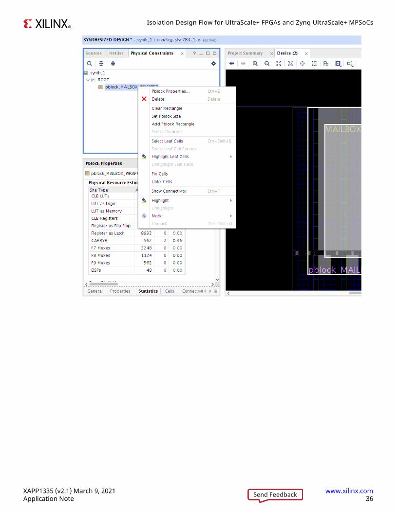
6. To delete the Pblock completely, in the Window drop down menu under Physical Constraints,right-click the Pblock entry, and click Delete as shown in the following figure.
Isolation Design Flow for UltraScale+ FPGAs and Zynq UltraScale+ MPSoCs
XAPP1335 (v2.1) March 9, 2021 www.xilinx.comApplication Note 35Send Feedback
Isolation Design Flow for UltraScale+ FPGAs and Zynq UltraScale+ MPSoCs
XAPP1335 (v2.1) March 9, 2021 www.xilinx.comApplication Note 36Send Feedback

When drawing Pblocks, you will see shaded resources that show you which resources areincluded in the Pblock and which are not. All resources not in a Pblock (non-shaded) arefences. In the following figure, the red shaded resources are allocated to one Pblock, thegreen shaded resources are allocated to a second Pblock, and the blue shaded resources areallocated to a third Pblock. The regions outlines are only guidance artifacts from creating thePblock and do not define resources. All non-shaded resources are fences, which means thoseresources are not being used.
Isolation Design Flow for UltraScale+ FPGAs and Zynq UltraScale+ MPSoCs
XAPP1335 (v2.1) March 9, 2021 www.xilinx.comApplication Note 37Send Feedback

Pblocks can be any shape and size as shown in the following figure. This design enablesgreen, red, and blue Pblocks to easily route to each other. The orange Pblock has all of thetop level logic, and the yellow Pblock routes the orange Pblock.
7. To complete the design and make sure your Pblock includes the required I/O Bank, assignpins. In this example, the orange Pblock contains the design I/Os.
In the drop-down menu, select IO Ports to display the I/O Ports window.
Note: In the following figure, the target I/O block is part of the orange Pblock. Ensure each PinAssignment is fixed and has the correct I/O standard; otherwise, the final design rule check (DRCs) ranunder Generate Bitstream will fail.
Isolation Design Flow for UltraScale+ FPGAs and Zynq UltraScale+ MPSoCs
XAPP1335 (v2.1) March 9, 2021 www.xilinx.comApplication Note 38Send Feedback

Drawing Pblocks Using Tcl CommandsWhen you draw Pblocks using the GUI as discussed above, the corresponding constraints getssaved to XDC files. In addition to using GUI, you can also use Tcl commands to create Pblocks byexecuting those commands in the Vivado Tcl Console or saving them in the XDC file. Thefollowing example uses one of the modules - MAILBOX_WRAPPER of XAPP1336 referencedesign to show how Tcl commands can be used as part of the XDC file to create an isolatedPblock.
IMPORTANT! The discussion in this section of doing floorplanning using Tcl commands is an advancedtopic. The same can be achieved by using Vivado GUI as explained in above section. This section can beused as reference if Pblocks need some fine adjustments or otherwise can be used for understanding howthe tools work behind the hood. Xilinx highly recommends to use Vivado GUI for Floorplanning.
create_pblock creates a Pblock that allows adding the logic instances inside it as shownbelow:
create_pblock pblock_MAILBOX_WRAPPER
add_cells_to_pblock command is then used to assign the isolated module's logic elements /instances to the newly created Pblock as shown below:
add_cells_to_pblock Pblock_MAILBOX_WRAPPER [get_cells[list design_1_i/MAILBOX_WRAPPER]-clear_locs
Isolation Design Flow for UltraScale+ FPGAs and Zynq UltraScale+ MPSoCs
XAPP1335 (v2.1) March 9, 2021 www.xilinx.comApplication Note 39Send Feedback

Once isolated modules/cells are assigned to the Pblock, the isolated Pblock must be assigned toa specific range of logics/PUs in the FPGA. Isolated regions/Pblocks can be defined in terms ofSLICEs, RAMB18s, RAMB36s, IOBs, ILOGICs, OLOGICs, IDELAYs, ODELAYs,PLLs, MMCME2s, IN_FIFOs, OUT_FIFOs, BUFGCTRLs, GTXs, DSP48s. Addingcomponents (specified range of sites) to an isolated Pblock is done by using the Tcl commandresize_pblock as shown below:
resize_pblock Pblock_MAILBOX_WRAPPER -add {SLICE_X2Y181:SLICE_X9Y239 BUFCE_LEAF_X16Y12:BUFCE_LEAF_X55Y15 BUFCE_ROW_FSR_X3Y3:BUFCE_ROW_FSR_X11Y3 DSP48E2_X0Y74:DSP48E2_X2Y95}
The generic format for the Tcl command for adding the ranges resize_pblock is:
resize_pblock -add {<comp name>_XaYb:<comp name>_XcYd
Where <comp name> = name of desired component, for example: SLICE, DSP48, and RAMB36,etc.
The component name can be identified by pointing at it in the Device view in the Vivado tool andreading it off the bottom right side of the screen. Coordinates can also be identified from thesame location that the component name was identified.
a, b, c, d = Coordinates of the starting component and the ending components
A full listing of this syntax can be found in Vivado Design Suite Tcl Command Reference Guide(UG835).
Note: While creating Pblocks, ensure that the SNAPPING_MODE property is set to FINE_GRAINED. See Derived Range and Snapping Mode section.
Note: Even though the physical resources are being added using the sites, the end goal is to capture theProgrammable Units in entirety and assign them to the Pblocks. See Pblocks and Programmable Unitssection.
Note: Nested Pblocks inside the isolated Pblocks is supported. Users can use nested Pblocks to meettiming closures. IDF supports only one level of nesting. Isolated Pblocks can have nested child Pblocksinside them, but the nested child Pblocks should not have child Pblocks.
Even if the design does not use DSP or block RAM PUs, they must be added to the isolated Pblock so thatthe routing resources contained by these PUs can be used. As a general rule, all available resources (exceptBUFGs and BUFHs i.e., global logics) should be assigned to the isolation Pblock unless there is specificneed to exclude that resource. This is the default selection when generating the XDC file if you use theVivado GUI tools as discussed above to create isolated Pblocks. If you are not familiar using Tcl commandsto create Pblocks and assign isolated modules to them, you are encouraged to use the Vivado GUI tools forthe same as explained in Drawing Pblocks for Floorplanning.
Isolation Design Flow for UltraScale+ FPGAs and Zynq UltraScale+ MPSoCs
XAPP1335 (v2.1) March 9, 2021 www.xilinx.comApplication Note 40Send Feedback

ConstraintsSome initial architecting and floorplanning of the FPGA/SoC, coupled with a list of constraints, isall that is required to achieve isolation of specific modules within a single FPGA or SoC. It isimportant to note that any logic that is not isolated is, by definition, unconstrained logic and canbe placed or routed by the tools in any isolated Pblock. Due to this, it is highly recommended thatonly global logic remains unconstrained, and global logic should be minimized. The followingexample shows the constraints generated by the tools when an isolated module is floorplannedinto a specific region of the device using Pblocks and Vivado GUI as discussed in the Floorplanning section.
As an example, isolation of the Pblock_MAILBOX_WRAPPER module of XAPP1336 is achievedby the following Tcl statements (commands):
create_pblock Pblock_MAILBOX_WRAPPERresize_pblock pblock_MAILBOX_WRAPPER -add {SLICE_X2Y181:SLICE_X9Y239 BUFCE_LEAF_X16Y12:BUFCE_LEAF_X55Y15 BUFCE_ROW_FSR_X3Y3:BUFCE_ROW_FSR_X11Y3 DSP48E2_X0Y74:DSP48E2_X2Y95}add_cells_to_pblock pblock_MAILBOX_WRAPPER [get_cells [list design_1_i/MAILBOX_WRAPPER]] -clear_locs
Vivado IDF Verifier (VIV) Checks 1,2,3, and 4The Vivado Isolation Verifier (VIV) verifies that an FPGA design partitioned into isolated Pblocksmeets stringent standards for fail-safe design. VIV is a collection of six design rule checks (DRCs)intended to aid FPGA developers in producing and documenting fault-tolerant FPGA applicationsdeveloped with the Xilinx Isolation Design Flow (IDF). Historically, VIV (VIV1) was a Tcl scriptthat ran in the Vivado tool framework in the form of user defined DRCs. As part of addingsupport of IDF for UltraScale+ architecture, Xilinx has released VIV2 which has the same set ofsix DRCs, but they are now are a part of Vivado built-in system DRCs. For convenience, in thisapplication note VIV2 will be referred to as VIV.
Vivado Isolation Verifier (VIV) 2.0 is available in Vivado® Design Suite 2018.3, and is enabled byexecuting the set_param hd.enableIDFDRC true command in Vivado’s Tcl Console. Refer toVivado Isolation Verifier User Guide (UG1291) for more detailed information on VIV2.
Isolation Design Flow for UltraScale+ FPGAs and Zynq UltraScale+ MPSoCs
XAPP1335 (v2.1) March 9, 2021 www.xilinx.comApplication Note 41Send Feedback

1. To run this tool, open the Report DRC window in the Reports drop-down menu as shown inthe following figure.
2. In the Rules window, under Isolation, select Provenance and Constraints, and click OK.
Isolation Design Flow for UltraScale+ FPGAs and Zynq UltraScale+ MPSoCs
XAPP1335 (v2.1) March 9, 2021 www.xilinx.comApplication Note 42Send Feedback

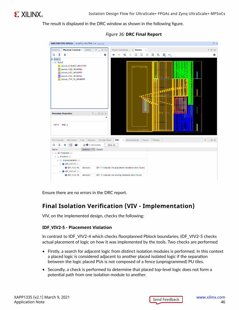
The result displays in the DRC window as shown in the following figure.
Ensure there are no errors in the DRC report and then run Implementation.
Constraint Check (VIV-Constraints)VIV, on the floorplan, checks the following:
IDF_VIV2-1 – Provenance:
IDF_VIV2-1 is an advisory DRC documenting the circumstances of the run. It also validates thatthe design has at least two modules marked as isolated (using the HD.ISOLATED property). Netsdriven by cells marked HD.ISOLATED_EXEMPT are exempt from inter-region isolation rules andare listed in the IDF_VIV2-1 output. This DRC also checks that the SNAPPING_MODE propertyof each Isolated Pblock is set to FINE_GRAINED.
IDF_VIV2-2 - I/O Bank Violation:
Pins from different isolation regions are not co-located in the same IOB bank.
Note: While VIV does fault such conditions, only specific security related applications require such bankisolation. Most applications allow sharing of IO banks. Bank sharing is dependent on the specificapplication and users need to take decision to allow bank sharing per use case basis.
Isolation Design Flow for UltraScale+ FPGAs and Zynq UltraScale+ MPSoCs
XAPP1335 (v2.1) March 9, 2021 www.xilinx.comApplication Note 43Send Feedback

IDF_VIV2-3 - Package Pin Violation:
Pins from different isolation groups are not physically adjacent, vertically or horizontally, at thedie level.
Pins from different isolation groups are not physically adjacent at the package level. Adjacency isdefined in eight compass directions: north, south, east, west, northeast, southeast, northwest,and southwest.
IDF_VIV2-4 - Floorplan Violation:
The Pblock constraints in the XDC file are defined by the user such that a minimum fence aslisted in Table 1 exists between isolated Pblocks. This means Pblocks are drawn with valid fencebetween them.
ImplementationThis step performs resource placement, which uses the Pblock isolation rules, followed byrouting which uses only trusted routes that avoids using routing resources in the fences.
Vivado Isolation Verifier (VIV) Checks 5 and 6After implementation completes (placement and routing) without any errors, VIV is run again onthe implemented design to validate that the required isolation is built into the design.
To run these DRCs, open the Report DRC window in the Reports drop-down menu, and selectImplementation under Isolation, as shown in the following figure.
Isolation Design Flow for UltraScale+ FPGAs and Zynq UltraScale+ MPSoCs
XAPP1335 (v2.1) March 9, 2021 www.xilinx.comApplication Note 44Send Feedback

Figure 35: Report DRC Window
Isolation Design Flow for UltraScale+ FPGAs and Zynq UltraScale+ MPSoCs
XAPP1335 (v2.1) March 9, 2021 www.xilinx.comApplication Note 45Send Feedback
The result is displayed in the DRC window as shown in the following figure.
Figure 36: DRC Final Report
Ensure there are no errors in the DRC report.
Final Isolation Verification (VIV - Implementation)VIV, on the implemented design, checks the following:
IDF_VIV2-5 - Placement Violation
In contrast to IDF_VIV2-4 which checks floorplanned Pblock boundaries, IDF_VIV2-5 checksactual placement of logic on how it was implemented by the tools. Two checks are performed
• Firstly, a search for adjacent logic from distinct isolation modules is performed. In this contexta placed logic is considered adjacent to another placed isolated logic if the separationbetween the logic placed PUs is not composed of a fence (unprogrammed) PU tiles.
• Secondly, a check is performed to determine that placed top-level logic does not form apotential path from one isolation module to another.
Isolation Design Flow for UltraScale+ FPGAs and Zynq UltraScale+ MPSoCs
XAPP1335 (v2.1) March 9, 2021 www.xilinx.comApplication Note 46Send Feedback

IDF_VIV2-6 - Routing Violation
Isolated routing must be separated by an adequate fence and trusted routing must satisfy thefollowing:
• Inter-region routes have loads in exactly one isolation group
• No routing switches (PIPs) are used in the fence
• Inter-region routes cannot share a tile unless source regions match and load regions match
• An intra-region route cannot enter a fence tile or an isolated tile of another isolation groupunless it is driven by a cell marked with the HD.ISOLATED_EXEMPT property
Note: Vivado tools automatically take care of the trusted routing and users do not need to do anythingextra other than having valid fences in their designs.
Design GuidanceConcept of OwnershipThis section is an extension of the ownership discussion in Mapping the Logical Ownership tothe Physical Ownership.
Logical OwnershipLogical ownership relates to HDL partition / isolation modules
• Each HDL file logically owns the logic instantiated within it.
• Only global logic (BUFG, MMCM etc.) is allowed at the top logical level of design.
• Only global logic can be at the top, but it can also instantiated in an isolated hierarchy if theHD.ISOLATED_EXEMPT property is used.
Physical OwnershipPhysical ownership relates to Isolated Regions (Pblocks)
• No user logic component can be used if it is not physically owned by an isolated Pblock.
○ Physical ownership is defined by the addition of the available components/PUs to theisolated Pblock definition in the XDC file/ Pblock drawn using Vivado GUI.
○ A Pblock is called isolated Pblock if it is mapped to an isolated module.
○ resize_Pblock constraint allows a range of slices placed in the Pblock to be used by thedeveloper.
• Global logic, while not typically owned by any isolated logic, must be associated with anyisolated Pblock, except for BUFGs and BUFHs. If the global logic is part of an isolated moduleand not a BUFG or BUFH, it must be associated with the isolated Pblock of that isolatedmodule. Additionally, remember to exempt global logic using HD.ISOLATED_EXEMPTproperty.
Isolation Design Flow for UltraScale+ FPGAs and Zynq UltraScale+ MPSoCs
XAPP1335 (v2.1) March 9, 2021 www.xilinx.comApplication Note 47Send Feedback

Trusted Routing RulesTrusted routing is automatic when HD.ISOLATED is set on the isolated modules of a design. Thedesign tools recognize the communication between isolated Pblocks and use the trusted routingresources. Thus, the tools do everything automatically for you. However, some rules must beadhered to if safe communication between isolated modules is to be guaranteed. The rulesoutlined in this section are a general guideline that the isolation designers must know withregards to the isolation routing concepts.
Note: The Vivado tools automatically follow each of the rules listed below. As a good design practice, it isrecommended to understand these IDF rules and take the suggested precautions to avoid violating them,even though Vivado tools takes the necessary steps to ensure that they are followed. The changes done bythe tools to incorporate trusted routing rules appear in the netlist after the synthesis phase.
Following are the rules listed for trusted routing:
Rule 1: Feed-through signals are not allowed without buffering of some kind such as LUT or FF.
• If a signal is directly connected to both an input port and an output port, it must be buffered
• Direct instantiation of a buffer (LUT1, for example) is recommended. This isolates the wiresegments in each of the isolated Pblocks with the LUT buffer, preventing a common (shorted)net throughout both regions
Problem: The following figure shows IDF rules violation because of the short between twoisolated Pblocks.
Figure 37: Short created by Feed-Trough Signal
Isolated Pblock2
Isolated Pblock 1
PAD IOB
Virtual short between two isolated pblcoks
X24364-081720
Solution: Feed-through signals need to be buffered. This can be achieved either through HDLcoding to ensure that there is some unique driver on the output port, by direct instantiation of aLUT, or flip-flop buffer as shown in the following figure, or by letting the Vivado tools address theissue using separate wire segments.
Isolation Design Flow for UltraScale+ FPGAs and Zynq UltraScale+ MPSoCs
XAPP1335 (v2.1) March 9, 2021 www.xilinx.comApplication Note 48Send Feedback

Figure 38: Elimination of Short by Instantiation of a LUT Buffer
Isolated Pblock2
Isolated Pblock1
PAD IOB
LUT
X24365-081720
Rule 2: An isolated module’s output port (driver) cannot connect to more than one isolatedmodule’s input port (load). Stated differently, port-to-port connections must be singular:
• Two different ports need to be created for such a connection.
• Each port must not violate Rule 3
Problem: In the following figure, the orange and blue colored nets creates a potential connectionbetween Isolated Module 2 and Isolated Module 3 which was never intended in the originaldesign, and hence violates isolation between Isolated Modules 2 and 3.
Figure 39: Multi-Port Connection Causing Connectivity between Isolated Module 2 andIsolated Module 3
Isolated Module 1 Isolated Module 2
Isolated Module 3
en
rst
potential connection
X24366-081720
Isolation Design Flow for UltraScale+ FPGAs and Zynq UltraScale+ MPSoCs
XAPP1335 (v2.1) March 9, 2021 www.xilinx.comApplication Note 49Send Feedback
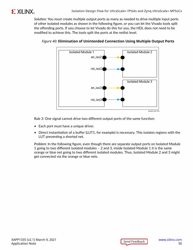
Solution: You must create multiple output ports as many as needed to drive multiple input portsof other isolated modules as shown in the following figure, or you can let the Vivado tools splitthe offending ports. If you choose to let Vivado do this for you, the HDL does not need to bemodified to achieve this. The tools split the ports at the netlist level.
Figure 40: Elimination of Unintended Connection Using Multiple Output Ports
Isolated Module 1 Isolated Module 2
Isolated Module 3
en_iso2
en_iso3
rst_iso2
rst_iso3
X24367-081720
Rule 3: One signal cannot drive two different output ports of the same function:
• Each port must have a unique driver.
• Direct instantiation of a buffer (LUT1, for example) is necessary. This isolates regions with theLUT preventing a shorted net.
Problem: In the following figure, even though there are separate output ports on Isolated Module1 going to two different isolated modules – 2 and 3, inside Isolated Module 1 it is the sameorange or blue net going to two different isolated modules. Thus, Isolated Module 2 and 3 mightget connected via the orange or blue nets.
Isolation Design Flow for UltraScale+ FPGAs and Zynq UltraScale+ MPSoCs
XAPP1335 (v2.1) March 9, 2021 www.xilinx.comApplication Note 50Send Feedback

Figure 41: Unintended Connectivity between Isolated Module 2 and Isolated Module 3Inside Isolated Module 1
Isolated Module 1 Isolated Module 2
Isolated Module 3
en_iso3
rst_iso3
en_iso2
rst_iso2
potential connection
X24368-081720
Another variant of this problem can be when driver of an isolated module drives itself as well asanother isolated module as shown in the following figure. This also violates the IDF rules forTrusted Routing.
Figure 42: Unintended Connectivity between Isolated Module 1 and Isolated Module 2
Isolated Module 1 Isolated Module 2
Load 2D Q
Q
SET
CLR
Load 1
X24369-081720
Solution: Each port driver needs to be buffered. This can be achieved through HDL coding toensure that there is some unique driver for each output port, by direct instantiation of a LUTbuffer or flip-flip as shown below in the following figures, or by letting the Vivado tools addressthe issue using separate wire segments.
Isolation Design Flow for UltraScale+ FPGAs and Zynq UltraScale+ MPSoCs
XAPP1335 (v2.1) March 9, 2021 www.xilinx.comApplication Note 51Send Feedback
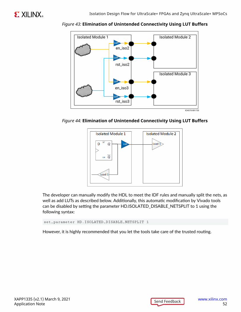
Figure 43: Elimination of Unintended Connectivity Using LUT Buffers
Isolated Module 1 Isolated Module 2
Isolated Module 3
LUT
LUT
LUT
LUT
en_iso2
rst_iso2
en_iso3
rst_iso3
X24370-081720
Figure 44: Elimination of Unintended Connectivity Using LUT Buffers
The developer can manually modify the HDL to meet the IDF rules and manually split the nets, aswell as add LUTs as described below. Additionally, this automatic modification by Vivado toolscan be disabled by setting the parameter HD.ISOLATED_DISABLE_NETSPLIT to 1 using thefollowing syntax:
set_parameter HD.ISOLATED_DISABLE_NETSPLIT 1
However, it is highly recommended that you let the tools take care of the trusted routing.
Isolation Design Flow for UltraScale+ FPGAs and Zynq UltraScale+ MPSoCs
XAPP1335 (v2.1) March 9, 2021 www.xilinx.comApplication Note 52Send Feedback
Hints and GuidelinesResources to Add in an Isolated PblockIt is generally advised to add all the available resources i.e. Programmable Units (PUs) within anisolated Pblock (except those that are needed for the fence), even if the logic tile/PU is not usedin the design, because excluding them also excludes using their respective routing resources.Failure to do so, while not an error, might produce designs that are very difficult to route. This istrue even for the I/O clock buffers.
However, in the Vivado tool, BUFGs and BUFHs must not be included in the isolated Pblocksunless you want the global clock isolated (not advisable unless the design warrants it to beisolated). All other components must be included.
Note: Resources that are not associated with a Pblock cannot be used even if it is needed by top level logic.Resources not assigned to any Pblock are invisible to placement and routing tools. If global clock in an IP isowned by any isolated module it needs to be exempted from isolation using HD.ISOLATION_EXEMPTproperty.
Shading PblocksLooking at Pblocks might be easy but user floorplans are not always simple. IDF highlyrecommends taking advantage of the highlighting features of Vivado. The following Tcl script willhighlight all the Pblocks in the design:
set pblocks [get_pblocks *];set ci 1;foreach pblock $pblocks {highlight_objects -color_index [expr {1 + ($ci % 19)}] [get_pblocks $pblock]; incr ci}
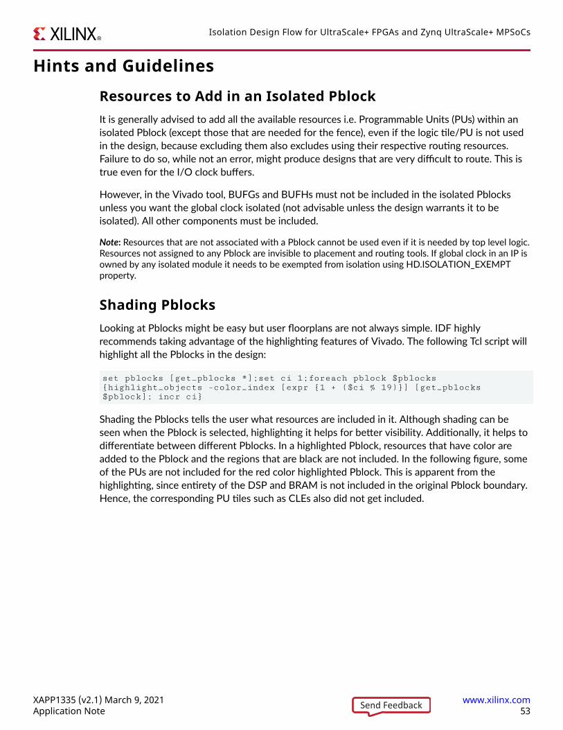
Shading the Pblocks tells the user what resources are included in it. Although shading can beseen when the Pblock is selected, highlighting it helps for better visibility. Additionally, it helps todifferentiate between different Pblocks. In a highlighted Pblock, resources that have color areadded to the Pblock and the regions that are black are not included. In the following figure, someof the PUs are not included for the red color highlighted Pblock. This is apparent from thehighlighting, since entirety of the DSP and BRAM is not included in the original Pblock boundary.Hence, the corresponding PU tiles such as CLEs also did not get included.
Isolation Design Flow for UltraScale+ FPGAs and Zynq UltraScale+ MPSoCs
XAPP1335 (v2.1) March 9, 2021 www.xilinx.comApplication Note 53Send Feedback

Figure 45: Shading of Pblocks for Better Visualization of Its Included Resources
DSP not fully enclosed so it’s complete PU is excluded from the Pblock
BRAM not fully enclosed soits complete PU is excludedfrom the Pblock
X24372-081720
HDIO versus HPIO PUs
HDIO
As listed in Table 1, HDIO has the following fence rule:
• Minimum fence width (vertical fence) is ½ HDIO
• Minimum fence height (horizontal fence) is ½ HDIO PU
HDIO PU is a special PU where ½ of it can be used as fence. That also means half of it can beincluded in a Pblock.
HPIO
As listed in Table 1, HPIO has the following fence rule:
• Minimum fence width (vertical fence) is 1 HPIO PU
• Minimum fence height (horizontal fence) is 1 HPIO PU
Isolation Design Flow for UltraScale+ FPGAs and Zynq UltraScale+ MPSoCs
XAPP1335 (v2.1) March 9, 2021 www.xilinx.comApplication Note 54Send Feedback
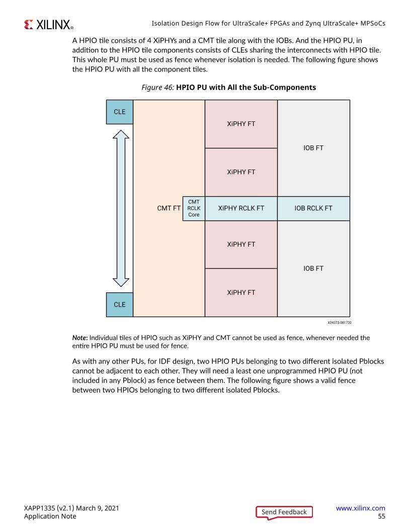
A HPIO tile consists of 4 XiPHYs and a CMT tile along with the IOBs. And the HPIO PU, inaddition to the HPIO tile components consists of CLEs sharing the interconnects with HPIO tile.This whole PU must be used as fence whenever isolation is needed. The following figure showsthe HPIO PU with all the component tiles.
Figure 46: HPIO PU with All the Sub-Components
CMT FT
IOB FT
XiPHY FT
XiPHY FT
XiPHY FT
XiPHY FT
IOB FT
XiPHY RCLK FT IOB RCLK FTCMT RCLK Core
CLE
CLE
X24373-081720
Note: Individual tiles of HPIO such as XiPHY and CMT cannot be used as fence, whenever needed theentire HPIO PU must be used for fence.
As with any other PUs, for IDF design, two HPIO PUs belonging to two different isolated Pblockscannot be adjacent to each other. They will need a least one unprogrammed HPIO PU (notincluded in any Pblock) as fence between them. The following figure shows a valid fencebetween two HPIOs belonging to two different isolated Pblocks.
Isolation Design Flow for UltraScale+ FPGAs and Zynq UltraScale+ MPSoCs
XAPP1335 (v2.1) March 9, 2021 www.xilinx.comApplication Note 55Send Feedback
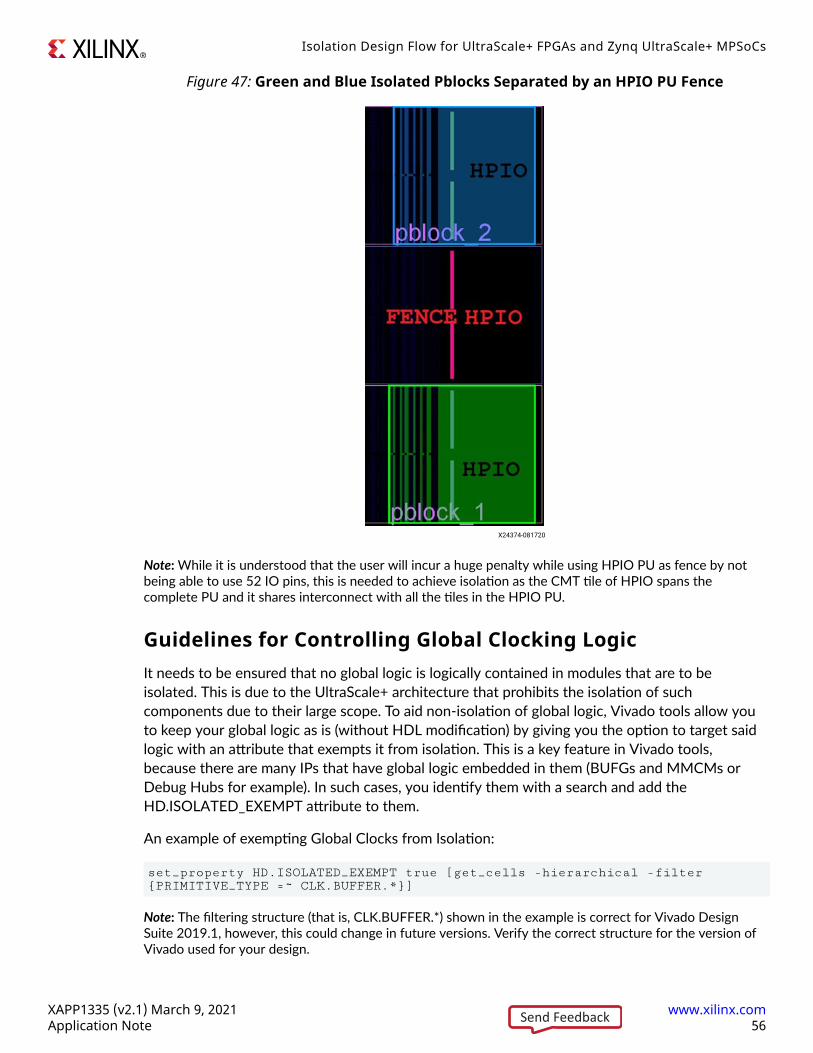
Figure 47: Green and Blue Isolated Pblocks Separated by an HPIO PU Fence
X24374-081720
Note: While it is understood that the user will incur a huge penalty while using HPIO PU as fence by notbeing able to use 52 IO pins, this is needed to achieve isolation as the CMT tile of HPIO spans thecomplete PU and it shares interconnect with all the tiles in the HPIO PU.
Guidelines for Controlling Global Clocking LogicIt needs to be ensured that no global logic is logically contained in modules that are to beisolated. This is due to the UltraScale+ architecture that prohibits the isolation of suchcomponents due to their large scope. To aid non-isolation of global logic, Vivado tools allow youto keep your global logic as is (without HDL modification) by giving you the option to target saidlogic with an attribute that exempts it from isolation. This is a key feature in Vivado tools,because there are many IPs that have global logic embedded in them (BUFGs and MMCMs orDebug Hubs for example). In such cases, you identify them with a search and add theHD.ISOLATED_EXEMPT attribute to them.
An example of exempting Global Clocks from Isolation:
set_property HD.ISOLATED_EXEMPT true [get_cells -hierarchical -filter{PRIMITIVE_TYPE =~ CLK.BUFFER.*}]
Note: The filtering structure (that is, CLK.BUFFER.*) shown in the example is correct for Vivado DesignSuite 2019.1, however, this could change in future versions. Verify the correct structure for the version ofVivado used for your design.
Isolation Design Flow for UltraScale+ FPGAs and Zynq UltraScale+ MPSoCs
XAPP1335 (v2.1) March 9, 2021 www.xilinx.comApplication Note 56Send Feedback

These filter statements are very generic (wild cards). More specific operations can be performedif there are some clocks that need exemption and some that do not.
Note: You do not apply the HD.ISOLATED_EXEMPT property on a net, you apply it to the cell that drivesthe net to exempt the net from isolation.
IMPORTANT! You cannot isolate clocks due to their global scope.
Vivado IP Integrator Differences – Creating WrappersVivado IP integrator is fully compatible with the Isolation Design Flow. In some cases, it evenmakes it easier, for example, the ability to add hierarchy with a single click/command.
However, there is one feature to be mindful of when creating isolated designs in Vivado IPintegrator. To preserve the IP being instantiated, IP integrator automatically adds theDONT_TOUCH property to all instances of IP. This is a good thing, because it adds the IPvendors’ IP without modification. However, this impacts the feature of IDF where isolated netscan drive multiple isolated regions. In this case, the Vivado tool attempts to split that net tofollow IDF rules but is prevented from doing so due to the DONT_TOUCH attribute. Thus, if anIP is to be marked as an isolated module, that IP must be wrapped with a level of hierarchy thatdoes not have the DONT_TOUCH attribute. In such cases, follow the Vivado Design Suite UserGuide: Implementation (UG904) to add a level of hierarchy to a module (a right-click operation).
Gaps in the FloorplanThere are apparent gaps in the floorplan as seen by the Vivado tool Device window's RoutingResources view (refer to the following three (3) figures). These gaps are an artifact of how thesoftware model is depicted in the Vivado IDE. Such gaps do not represent any form of isolationand cannot be used as a fence because they are not, in fact a PU/tile at all.
The following are the most common gaps seen in the floorplan:
• RCLK row (regional clock row)
• Configuration blocks near the center of the device floorplan
• Boundary of clock regions
RCLK Row GapsThe RCLK row, in the center of each clock region, appears as a gap in the FPGA. The followingfigure shows such a gap highlighted by a white rectangle. Do not mistake this gap as a validfence.
Isolation Design Flow for UltraScale+ FPGAs and Zynq UltraScale+ MPSoCs
XAPP1335 (v2.1) March 9, 2021 www.xilinx.comApplication Note 57Send Feedback

Figure 48: RCLK Row Highlighted by White Rectangle That Looks like Fence, but It IsNot
RCLK row
X24375-081720
Configuration Blocks GapThere are some configuration blocks in the FPGA that looks like gaps but are not a fence. Thefollowing figure highlights such a gap with a white rectangle. These blocks cannot be used as afence. However, a valid BRAM PU fence has been shown with green rectangle.
Note: The following figure shows the routing view in Vivado. It is highly recommended to always usedevice view in Vivado to look at fences and create Pblocks while using IDF. The routing view is good fordetermining PUs if needed.
Figure 49: Config Block Highlighted in White Rectangle Looks like a Fence, but It IsNot
Config block
BRAM PU Fence
X24376-081720
Isolation Design Flow for UltraScale+ FPGAs and Zynq UltraScale+ MPSoCs
XAPP1335 (v2.1) March 9, 2021 www.xilinx.comApplication Note 58Send Feedback

Boundary of Clock RegionsGaps can be seen at the boundary of the clock regions. These are not valid fences and do notprovide any isolation. The following figure shows such a gap as that is seen in Vivado GUI.
Figure 50: Gap between Two Clock Regions Highlighted in White Rectangle That Lookslike a Fence, but It Is Not
Automatic Movement of IOB into Isolated HierarchyThe automatic insertion of IOBs into the intended isolated hierarchy is a feature of the VivadoDesign Suite. Before Vivado tools, you had to manually instantiate IOBs inside of the HDL foreach isolated module. Vivado tools, however, do this for you provided you have not alreadyinstantiated the IOB themselves. At initial inference, all IOB are at top level. Wherever VivadoIDF can see a clear usage for the IOB, it automatically moves this IOB from the top level into thedesired isolated module. This movement happens in the Vivado synthesis and/or the opt_designstep after synthesis but before placement.
However, there are some limitations to this feature because not all possible cases allow for suchmovement. These cases are as follows:
Case 1
Input with multiple destinations (that includes the top level). See the following figure.
Isolation Design Flow for UltraScale+ FPGAs and Zynq UltraScale+ MPSoCs
XAPP1335 (v2.1) March 9, 2021 www.xilinx.comApplication Note 59Send Feedback

Figure 51: Case 1 Block
TOP Level
MM
CM
PAD IsolatedModuleIOB
X24378-081720
In this case, a "reset" input to the top level MMCM also connects to at least on isolated region.
Case 2
Output whose input drives the IOB in question and at least one other region. See the followingfigure.
Figure 52: Case 2 Block
TOP Level
PADIsolated
Module #1 IOB
IsolatedModule #2
X24379-081720
Isolation Design Flow for UltraScale+ FPGAs and Zynq UltraScale+ MPSoCs
XAPP1335 (v2.1) March 9, 2021 www.xilinx.comApplication Note 60Send Feedback

Case 3
Output whose input comes directly from an input port of the isolated module in question. Seethe following figure.
Figure 53: Case 3 Block
TOP Level
PAD
IsolatedModule
IOB
X24380-081720
Note: It does not matter if that signal is used in the isolated module in question or not.
Case 4
Bidirectional IOB where input and output do not go to the same isolated region. See thefollowing figure.
Isolation Design Flow for UltraScale+ FPGAs and Zynq UltraScale+ MPSoCs
XAPP1335 (v2.1) March 9, 2021 www.xilinx.comApplication Note 61Send Feedback

Figure 54: Case 4 Block
TOP Level
IsolatedModule #1
IOB
IsolatedModule #2
IOB
PAD
X24381-081720
Case 5
IOB with connections only to top level logic. See the following figure.
Figure 55: Case 5 Block
MMCMPAD
IsolatedModule
IOB
TOP Level
X24382-081720
Note: Top level IOB driving only top-level logic will not be moved
Case 6
IOB was manually instantiated by the user on their IP.
Isolation Design Flow for UltraScale+ FPGAs and Zynq UltraScale+ MPSoCs
XAPP1335 (v2.1) March 9, 2021 www.xilinx.comApplication Note 62Send Feedback

Directly instantiated IOB with the DONT_TOUCH property set on the buffer will not be moved.The DONT_TOUCH property can be inherited from the IP that instantiates the IOB or you canmanually add the property.
IDF Rules ChecklistThe following checklist is a helpful set of items which you can use to verify that all the basic rulesand guidelines for an IDF design are followed. The checklist can be used before, during, or afterproject design to help ensure the rules have been followed and to determine if overall good IDFdesign practices have been considered.
IDF Checklist
• The HD.ISOLATED property is applied to all isolated modules (except global clockingmodules).
• All isolated modules have corresponding Pblocks associated with them.
• Pblocks must contain the required resource types in enough quantities to implement theintended function or functions.
• Map out Pblocks that need connectivity and those that need IOBs for better floorplanningstrategy.
• Each isolated module must be in its own level of hierarchy.
○ Isolated modules cannot be nested
• A valid isolation fence (unused PU) must exist between Pblocks.
○ The fence is constructed indirectly by the space between isolated regions / Pblocks.
○ Refer to Table 1 for creating a valid fence.
○ Fence size is determined through schematic analysis and stated in rules and guidelinesthroughout this document.
○ Use the minimum fence width/height to maximize routing resources.
○ Bigger fence is not better. A bigger fence will not increase fault immunity but instead mightimpact timing due to a reduction in the availability of trusted routes.
• Isolated modules that communicate with each other must share a coincident Pblock edgeseparated by a valid fence otherwise routing might fail.
• Pblocks must enclose all available tiles in the device except the ones needs for minimum fencesize (only the fence remains).
○ Do not leave large gaps because the gaps do not provide an advantage and can even resultin routing difficulty.
○ Making the fence larger than necessary can make it difficult or impossible for inter-regionsignals (trusted routes) to cross the fence.
- For example, IDF rules prevent routing touchdowns in the fence. A fence size of one PU(the minimum fence size allowed) prohibits the use of all routes (to cross the fence) thatspan only a single PU. Larger fences further limit the routing resources available.
Isolation Design Flow for UltraScale+ FPGAs and Zynq UltraScale+ MPSoCs
XAPP1335 (v2.1) March 9, 2021 www.xilinx.comApplication Note 63Send Feedback

• Only global clocking logic should not be isolated. All other logic should be associated with anisolated module and placed in the associated isolated Pblock.
• For global logic instantiated within an isolated module, the HD.ISOLATED_EXEMPT propertymust be set (TRUE) for the tools to route to or from that global logic.
• Feed-through signals are not allowed without buffering of some kind (LUT, FF, etc.).
○ Vivado does this automatically unless you choose to disable this feature
• Ports communicating between two isolated modules can only have one source and onedestination.
○ Vivado does this automatically unless you choose to disable this feature
• IOBs must be instantiated or inferred inside isolated modules for proper isolation of the IOB.
○ Vivado does this automatically unless you choose to disable this feature.
• These are the limitations on Vivado automatically inserting IOBs
○ Input with multiple destinations, including top-level (i.e., reset to MMCM and isolatedmodule)
○ Output whose input drives the IOB in question and at least one other region, including top-level
○ Output whose input comes directly from an input port of the isolated module in question
○ Bidirectional IOB where input and output do not go to the same isolated region
○ IOB with connections only to top level. Top level IOB driving only top-level logic will not bemoved.
○ IOB was manually instantiated by you or the IP.
- Directly instantiated IOB with the DONT_TOUCH property set on the buffer will not bemoved. The DONT_TOUCH property can be inherited by the IP that instantiates theIOB or you can add it directly.
• Enable VIV by executing the Tcl command set_param hd.enableIDFDRC true inVivado’s Tcl console.
• Run Xilinx Vivado Isolation Verifier (VIV) on the elaborated design (constraint checking) tocheck for DRC violations for device and package pins (pin adjacency) and for IOB bankviolations (if required).
• Run Xilinx VIV on the placed and routed (implemented) design to check for DRC violations forIsolation violations.
Isolation Design ExampleAn isolation design example is provided in the Isolation Design Example for Zynq Ultrascale+MPSoC Application Note (XAPP1336) and is used throughout this application note to describe thedesign details and tool flow. For detailed information, see Isolation Design Flow.
Isolation Design Flow for UltraScale+ FPGAs and Zynq UltraScale+ MPSoCs
XAPP1335 (v2.1) March 9, 2021 www.xilinx.comApplication Note 64Send Feedback

IDF+DFXOverview of IDF+DFXThe Isolation Design Flow (IDF) and Dynamic Function eXchange (DFX) are two productionsolutions from Xilinx. They have been available for Zynq UltraScale+ devices from Vivado 2018.3onwards. From Vivado 2020.2 onwards, Xilinx supports combined flow of IDF and DFX. Thedocument is written with the assumption that the reader is familiar with both IDF and DFXmethodologies. For details on these individual methodologies, the user may refer to IsolationDesign Flow in this application note, Vivado Isolation Verifier User Guide (UG1291), Isolation DesignExample for Zynq Ultrascale+ MPSoC Application Note (XAPP1336), Vivado Design Suite User Guide:Dynamic Function eXchange (UG909), and Vivado Design Suite Tutorial: Dynamic Function eXchange(UG947). With this combined support, the user can create nested isolated modules (IM) insidereconfigurable partition (RP). Sample design hierarchy structure looks like the following exampleprovided here.
Figure 56: IDF+DFX Design Hierarchy
Isolation Design Flow for UltraScale+ FPGAs and Zynq UltraScale+ MPSoCs
XAPP1335 (v2.1) March 9, 2021 www.xilinx.comApplication Note 65Send Feedback

These isolated and reconfigurable regions require a floorplan that defines the overall usage of thedevice. An example floorplan might look like this:
Figure 57: Example Floorplan for IDF+DFX Design
The reconfigurable partition can have one or more reconfigurable modules that will bedynamically exchanged by way of partial bitstream delivery, most likely via the processing system(PS). Users must develop their own solution for delivering partial bitstreams and handling anyruntime tasks (logical decoupling of the dynamic region, updates to drivers associated withreconfigured peripherals).
Xilinx supports isolation design flow (IDF) with one or more reconfigurable partitions (RP). Userscan have one or more isolated modules (IM) inside the RP region or outside the RP region (inStatic region). The support for change of composition (hierarchy, floorplan) of the nested IMsinside the RP from one reconfigurable module (RM) to the next is limited. It is stronglyrecommended to keep the same floorplan for each configuration. The complete support for thiswill be added in future Vivado releases.
Use cases that are NOT supported include:
Isolation Design Flow for UltraScale+ FPGAs and Zynq UltraScale+ MPSoCs
XAPP1335 (v2.1) March 9, 2021 www.xilinx.comApplication Note 66Send Feedback

• Nesting an isolated region within an isolated region
• Nesting a reconfigurable partition within an isolated region
• Nesting of a reconfigurable partition within a reconfigurable partition and then an isolatedpartition under that.
• Identifying a single module as both reconfigurable and isolated
This last exception can be effectively supported by directly instantiating a level of hierarchy suchthat an isolated module is directly below a reconfigurable partition and their floorplans areidentical.
Enable IDF+DFX FlowA combined flow of IDF+DFX is enabled by default for all Zynq UltraScale+ MPSoC devices butthe user need to set a param to enable the appropriate set of design rule checks for IDF+DFX.Users need to enable IDF and DFX separately as mentioned in the Isolation Design Flow of thisdocument and in the Vivado Design Suite User Guide: Dynamic Function eXchange (UG909). Toenable IDF+DFX DRCs, set the following parameter.
set_param hd.enableIDFDRC 1
This parameter information is not stored in the database so must be re-enabled in each Vivadosession. The parameter is most easily set in your vivado_init.tcl. For more details on howto run VIV DRCs, refer to Vivado IDF Verifier (VIV) Checks 1,2,3, and 4 and Vivado IsolationVerifier (VIV) Checks 5 and 6 of this document.
Both the project mode and the non-project Tcl scripted mode are supported. The DFX flow for IPIntegrator, however, is still in early access. You may refer to the Isolation Design Flow of thisdocument and Vivado Design Suite User Guide: Dynamic Function eXchange (UG909) for flowrequirements and details for topics such as:
• The use of HD.ISOLATED and HD.RECONFIGURABLE to define the functionality of a givenlevel of hierarchy
• Fence creation guidelines and rules for IO and clocks for the isolation design flow
• Logical decoupling and partial bitstream delivery for the dynamic function eXchange flow
Routing expansion in IDF+DFX flow works same as DFX flow. The reconfigurable partition in thecombined IDF+DFX solution is subject to more stringent regulations given the isolated modulesthat surround it. These additional rules must be considered when floorplanning thereconfigurable partition, and when designing each RM that will be placed in that RP:
• Expanded routing for RPs is enabled, but routing is contained per isolated module to followIDF rules
• No embedded clocks are allowed within an isolated module within any reconfigurable module
• Each interface on the reconfigurable partition must connect to only one isolated moduleoutside the RP*
Note: *Features planned for the future Vivado releases.
Isolation Design Flow for UltraScale+ FPGAs and Zynq UltraScale+ MPSoCs
XAPP1335 (v2.1) March 9, 2021 www.xilinx.comApplication Note 67Send Feedback

For this last item, the current requirement is that a trusted route starts in one IM and connects toonly one other IM; no net splitting is supported. If a trusted route must go to more than one IM,the user must create additional drivers and ports that will each connect to a single IM. Thefollowing image shows one unsupported scenario in Vivado 2020.2. A similar scenario of a driverin a static IM driving loads in multiple IMs, at least one of which is within an reconfigurablepartition (RP), would also be unsupported.
Figure 58: Unsupported Connectivity That Requires Net Splitting
While net splitting is not currently supported by the tools, it can be done manually. The supportfor automatic net splitting will be added in future Vivado releases.
Isolation Design Flow for UltraScale+ FPGAs and Zynq UltraScale+ MPSoCs
XAPP1335 (v2.1) March 9, 2021 www.xilinx.comApplication Note 68Send Feedback

Figure 59: Workaround Using Replication of Drivers
Floorplan Rules and GuidanceBoth isolated modules and reconfigurable partitions require Pblocks to identify resources tocontain these respective parts of the design. You may follow requirements for the respectivemodule type as documented in each user guide. The combined IDF+DFX solution adds moredesign rule checks (DRCs); run these interactively as you build the floorplan and watch for criticalwarnings as the implementation flow is run.
The most fundamental rule is that the Pblock ranges for any isolated module within areconfigurable partition be completely contained within the RP Pblock. Standard fence rulesapply regardless of where the isolated module Pblock exists. The fence can be either inside oroutside of the RP Pblock.
This collection of RMs for the one reconfigurable partition in the design may have differentinternal floorplans for the isolated regions contained within, but the interface port list mustremain consistent, per DFX rules. The two RMs shown in the following figures are legal and noextra guidance is needed to account for the different sizes of isolated modules within RM1 andRM2.
Isolation Design Flow for UltraScale+ FPGAs and Zynq UltraScale+ MPSoCs
XAPP1335 (v2.1) March 9, 2021 www.xilinx.comApplication Note 69Send Feedback

Figure 60: Different Isolation Pblocks within the Reconfigurable Partition
Figure 61: Different Isolation Pblocks within the Reconfigurable Partition
Nested Pblocks inside the isolated Pblocks are supported. Users can use nested Pblocks to meettiming closures. However, nested IDF Pblocks (isolated Pblock inside another isolated Pblock),nested DFX (DFX Pblock inside another DFX Pblock) and DFX Pblock inside the isolated Pblock,are not supported. The nested Pblocks inherit the properties of the parent. For example,IS_SOFT is false for the nested Pblocks. The support to change the properties will be added infuture Vivado releases.
One more limitation for the nested Pblocks is that net splitting will fail if the driver or load is inthe nested Pblock. The support for this will be added in future Vivado releases.
Isolation Design Flow for UltraScale+ FPGAs and Zynq UltraScale+ MPSoCs
XAPP1335 (v2.1) March 9, 2021 www.xilinx.comApplication Note 70Send Feedback
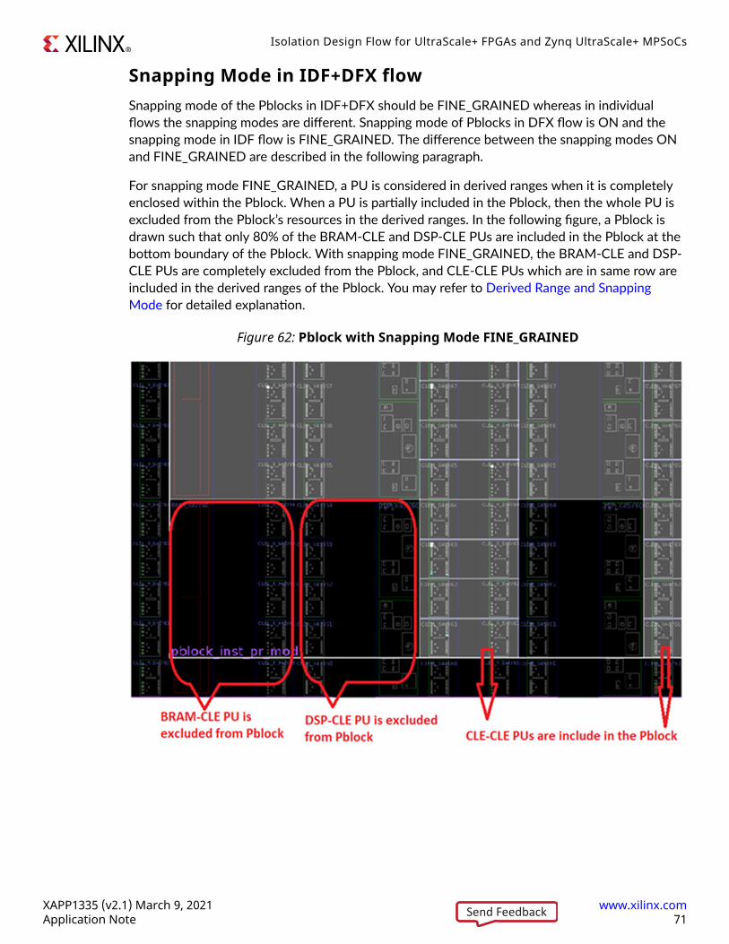
Snapping Mode in IDF+DFX flowSnapping mode of the Pblocks in IDF+DFX should be FINE_GRAINED whereas in individualflows the snapping modes are different. Snapping mode of Pblocks in DFX flow is ON and thesnapping mode in IDF flow is FINE_GRAINED. The difference between the snapping modes ONand FINE_GRAINED are described in the following paragraph.
For snapping mode FINE_GRAINED, a PU is considered in derived ranges when it is completelyenclosed within the Pblock. When a PU is partially included in the Pblock, then the whole PU isexcluded from the Pblock’s resources in the derived ranges. In the following figure, a Pblock isdrawn such that only 80% of the BRAM-CLE and DSP-CLE PUs are included in the Pblock at thebottom boundary of the Pblock. With snapping mode FINE_GRAINED, the BRAM-CLE and DSP-CLE PUs are completely excluded from the Pblock, and CLE-CLE PUs which are in same row areincluded in the derived ranges of the Pblock. You may refer to Derived Range and SnappingMode for detailed explanation.
Figure 62: Pblock with Snapping Mode FINE_GRAINED
Isolation Design Flow for UltraScale+ FPGAs and Zynq UltraScale+ MPSoCs
XAPP1335 (v2.1) March 9, 2021 www.xilinx.comApplication Note 71Send Feedback

For snapping mode ON when a PU is partially included in the Pblock, then the whole PU isexcluded from the derived ranges of the Pblock. This is the same as with the snapping modeFINE_GRAINED and additionally, CLE-CLE PUs in the same row are also excluded from thePblock derived ranges. The following figure of a Pblock is drawn such that it displays only 80% ofthe BRAM-CLE and DSP-CLE PUs included in the Pblock, at the bottom boundary of the Pblock.With snapping mode ON, the BRAM-CLE and DSP-CLE PUs are completely excluded from thePblock derived ranges and also the CLE-CLE PUs which are in same row are also excluded fromthe derived ranges of the Pblock. So, the Pblock boundary is always rectangle with snappingmode ON.
Figure 63: Pblock with Snapping Mode ON
With the same boundary, Pblock with snapping mode FINE_GRAINED includes more resourcesinto the derived ranges of the Pblock, than the Pblock with snapping mode ON.
Isolation Design Flow for UltraScale+ FPGAs and Zynq UltraScale+ MPSoCs
XAPP1335 (v2.1) March 9, 2021 www.xilinx.comApplication Note 72Send Feedback

Fence Rules in IDF+DFXFence rules are the same as the normal IDF flow, you may refer to the Isolation Fence section formore details. Fence is needed only between IM Pblocks, irrespective of whether they are nestedIM Pblocks or static IM Pblocks. A fence is not needed between the DFX Pblock and IM Pblock.A fence between the static IM Pblock and nested IM Pblock can be inside of the DFX Pblock oroutside the DFX Pblock.
In the following figure, the DFX Pblock and the nested IM Pblock shares the same boundaries,and the fence between the nested IM Pblock and the static IM Pblock is outside of the DFXPblock.
Figure 64: Fence Outside of the DFX Pblock
In the following figure, there is no gap between the DFX Pblock and the static IM Pblock, and thefence between the nested IM Pblock and the static Pblock is inside of the DFX Pblock.
Isolation Design Flow for UltraScale+ FPGAs and Zynq UltraScale+ MPSoCs
XAPP1335 (v2.1) March 9, 2021 www.xilinx.comApplication Note 73Send Feedback

Figure 65: Fence Inside of the DFX Pblock
Nested IM Pblocks inside of the DFX Pblock also need a fence and follows standard IDF fencerules. The fence between the nested IM Pblocks is always inside of the DFX Pblock. In thefollowing figure, nested IM Pblock1 and nested IM Pblock2 has an 1PU fence inside of the DFXPblock.
Figure 66: Fence Between the Nested IM Pblocks
Isolation Design Flow for UltraScale+ FPGAs and Zynq UltraScale+ MPSoCs
XAPP1335 (v2.1) March 9, 2021 www.xilinx.comApplication Note 74Send Feedback

The following image is the complete example floorplan with two static IM Pblocks, and twonested IM Pblocks inside of a DFX Pblock.
Figure 67: IDF+DFX Example Floorplan with Fences
Similarly, the fence between the nested IM Pblocks of two DFX Pblocks can be inside either ofthe DFX Pblock or outside of the two DFX Pblocks.
IDF + DFX SummaryThis section gives high level details on how to combine IDF and DFX flows in a single design. Youmay refer to Vivado Design Suite Tutorial: Dynamic Function eXchange (UG947) for a detailedexplanation on DFX design creation and Isolation Design Example for Zynq Ultrascale+ MPSoCApplication Note (XAPP1336) for IDF design creation.
The following steps outline how to combine IDF and DFX flows in a single design.
• Follow the DFX flow by referring to Vivado Design Suite Tutorial: Dynamic Function eXchange(UG947) till the synthesis and generate synth DCPs or static top-level design and for eachDFX module.
Isolation Design Flow for UltraScale+ FPGAs and Zynq UltraScale+ MPSoCs
XAPP1335 (v2.1) March 9, 2021 www.xilinx.comApplication Note 75Send Feedback
• Enable IDF flow in all the DCPs. First, open the static dcp and set HD.ISOLATED to true onthe modules and save the dcp. Similarly, you may open all the RM DCPs and setHD.ISOLATED to true and then save the DCPs.
• Enable IDF DRCs by setting hd.enableIDFDRC to true.
• Link the entire design for the first configuration using the link_design command. Some of theIDF optimizations related to net-splitting and IO buffer insertion takes place in the link_designphase. Ensure the IDF is enables on the synth DCPs before the link_design.
• Next, floorplan the design. The best way to do is step-by-step floorplanning. First, do thefloorplanning for reconfigurable partitions. Follow the guidelines from Vivado Design Suite UserGuide: Dynamic Function eXchange (UG909) and Vivado Design Suite Tutorial: Dynamic FunctioneXchange (UG947) and draw the Pblocks for reconfigurable partitions. Run the DynamicFunction eXchange DRCs and ensure there are no DRC errors.
• Draw Pblocks for isolated modules including nested modules inside of the PR by following theIDF and IDF+DFX floorplanning guidelines mentioned in this document. You may refer to Drawing Pblocks Using Vivado GUI section for drawing Pblocks using Vivado GUI.
• Run VIV DRCs and ensure there are no warnings or errors. You may refer to Vivado IsolationVerifier User Guide (UG1291) on how to run the VIV DRCs.
• Save these Pblocks and associated properties. A script is provided with Vivado Design SuiteTutorial: Dynamic Function eXchange (UG947) design files to save the Pblocks. It is advised tosave static Pblocks and RP Pblocks in a single XDC file and nested IM Pblocks inside each RMin a separate file. You may use the script with Pblocks option.
• Implement the design using the standard DFX implementation flow.
• Run VIV DRCs on implemented design. You may refer to Vivado Isolation Verifier User Guide(UG1291) on how to run VIV DRCs. Ensure there are no warnings or errors.
• Generate black box dcp and static routing dcp by following the steps from Vivado Design SuiteTutorial: Dynamic Function eXchange (UG947).
Isolation Design Flow for UltraScale+ FPGAs and Zynq UltraScale+ MPSoCs
XAPP1335 (v2.1) March 9, 2021 www.xilinx.comApplication Note 76Send Feedback

Figure 68: IDF+DFX Design Flow Steps
Isolation Design Flow for UltraScale+ FPGAs and Zynq UltraScale+ MPSoCs
XAPP1335 (v2.1) March 9, 2021 www.xilinx.comApplication Note 77Send Feedback

Second Configuration• Link the complete design for second configuration using the top static route dcp and RM
synth dcps. You may refer to Vivado Design Suite Tutorial: Dynamic Function eXchange (UG947)for further details.
• The static route dcp does not contain floorplanning information for nested IMs inside of theRP. It contains Pblock information for static IMs and PR region only.
• If there is no change in the hierarchy and floorplan inside the PR from the previousconfiguration, then use the already saved XDC file and load the floorplan for nested IMs. Ifthere is a change in the hierarchy or floorplan, then create new floorplanning by following IDFand IDF+DFX guidelines. Refer to the Drawing Pblocks Using Vivado GUI section for drawingPblocks using the Vivado GUI.
• Run VIV DRC checks 1, 2, 3, and 4. Refer to Vivado Isolation Verifier User Guide (UG1291) onhow to select and run VIV DRCs. Do not run VIV implementation DRCs (check 5 and 6) at thispoint as the design is not implemented yet. Ensure there are no DRC warnings or error.
• Save the Pblocks for nested IMs. You can use the script provided with Vivado Design SuiteTutorial: Dynamic Function eXchange (UG947).
• Implement the design by using the standard DFX implementation flow.
• Run all VIV DRC checks on the implemented design. Ensure there are no warnings or errors.
You may similarly implement all the configurations. For pr_verify, bitstream generation, and forloading the FPGA, follow the standard DFX flow.
Isolation Design Flow for UltraScale+ FPGAs and Zynq UltraScale+ MPSoCs
XAPP1335 (v2.1) March 9, 2021 www.xilinx.comApplication Note 78Send Feedback
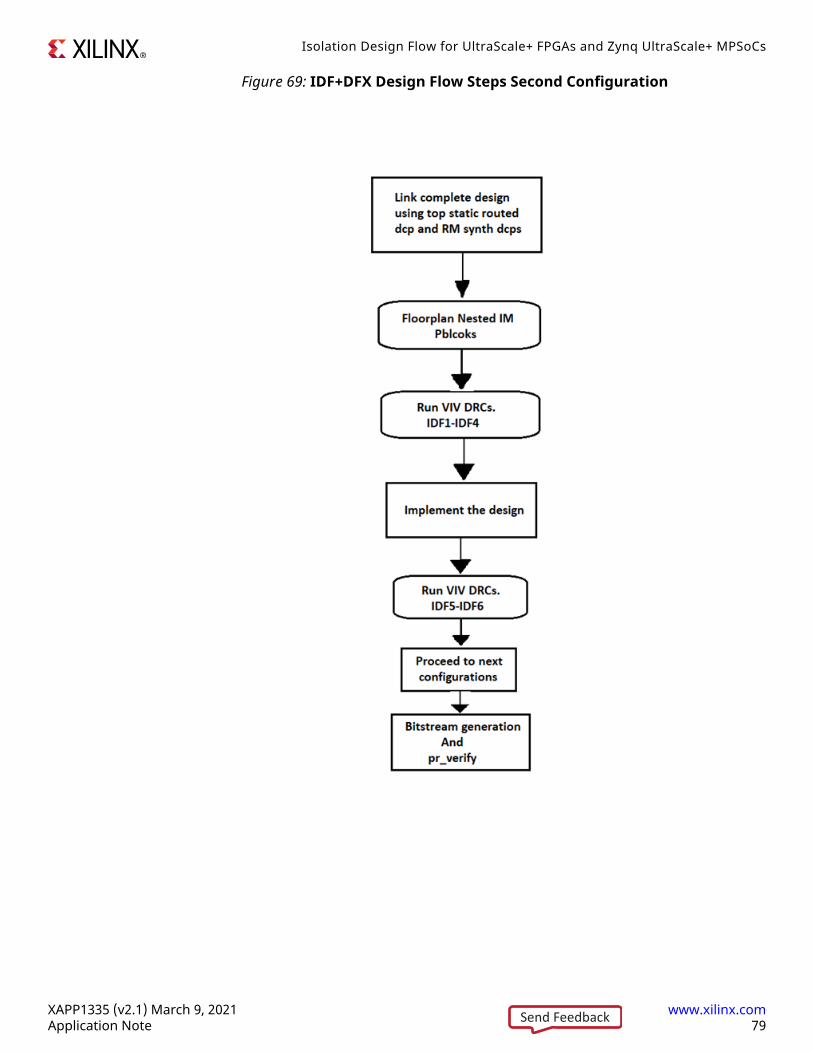
Figure 69: IDF+DFX Design Flow Steps Second Configuration
Isolation Design Flow for UltraScale+ FPGAs and Zynq UltraScale+ MPSoCs
XAPP1335 (v2.1) March 9, 2021 www.xilinx.comApplication Note 79Send Feedback

Supported/Unsupported FeaturesThis section lists the current supported and unsupported features. While future enhancementsmay be possible, this list is not an indication that these enhancements will be delivered in afuture revision.
Supported Features• Device support: All Zynq UltraScale+ MPSoC
• One or more reconfigurable partitions alongside of one or more isolated regions
Unsupported FeaturesSome features are not yet implemented but could be planned for future releases, where noted.
• UltraScale™ and Versal™ architectures, Virtex®, and Kintex® UltraScale+ devices.
• Zynq UltraScale+ RFSoC devices
• Nesting a reconfigurable partition within an isolated module
• Net splitting, as documented above
Known Limitations• Clocks cannot be isolated from the other clocks.
ConclusionThe focus of this document is to help design engineering professionals understand the newfeatures and limitations of implementing the Xilinx® Isolation Design Flow (IDF) technology withUltraScale+™ architecture and Zynq® UltraScale+™ MPSoC programmable logic (PL). It helpsimplement the IDF technology as part of your overall layers of protection strategy used infunctional safety and security design architectures. Although the impact of using IDF is notdiscussed in this document, you are encouraged to discuss such solutions with your Xilinx FieldApplication Engineer or other Xilinx resources. This document also discusses about IDF+DFXdesign flow. The Isolation Design Flow (IDF) and Dynamic Function eXchange (DFX) are twoproduction solutions from Xilinx.
References1. UltraFast Design Methodology Guide for Xilinx FPGAs and SoCs (UG949)
2. Vivado Isolation Verifier User Guide (UG1291)
3. UltraScale Architecture Configuration User Guide (UG570)
4. Vivado Design Suite User Guide: Hierarchical Design (UG905)
5. Soft Error Mitigation Controller LogiCORE IP Product Guide (PG036)
Isolation Design Flow for UltraScale+ FPGAs and Zynq UltraScale+ MPSoCs
XAPP1335 (v2.1) March 9, 2021 www.xilinx.comApplication Note 80Send Feedback

6. UltraScale Architecture Memory Resources User Guide (UG573)
7. Triple Modular Redundancy (TMR) LogiCORE IP Product Guide (PG268)
8. Vivado Design Suite Tcl Command Reference Guide (UG835)
9. UltraScale Architecture Clocking Resources User Guide (UG572)
10. Vivado Design Suite User Guide: Dynamic Function eXchange (UG909)
11. Vivado Design Suite Tutorial: Dynamic Function eXchange (UG947)
12. Isolation Design Example for Zynq Ultrascale+ MPSoC Application Note (XAPP1336)
13. Calculating Zynq-7000 Failure Rates for Functional Safety Applications (XAPP1279)
14. Calculating Artix-7 Failure Rates for Functional Safety Applications (XAPP1310)
15. Calculating Spartan-7 Failure Rates for Functional Safety Applications (XAPP1325)
Note: References 11 through 13 are available from the Functional Safety lounge.
Revision HistoryThe following table shows the revision history for this document.
Section Revision Summary03/09/2021 Version 2.1
IDF+DFX Added several new sections and images for more clarity oncombined IDF+DFX flow.
10/09/2020 Version 2.0
Isolation Properties, Isolation Modules, and Communicationbetween Isolated Modules
Added new sections for more clarity on the HD.ISOLATEDand HD.ISOLATED_EXEMPTION properties.
Derived Range and Snapping Mode Added new sections for more clarity on how placement androuting resources are added in Pblocks.
Mapping the Logical Ownership to the Physical Ownership Added a new section for more clarity on link between logicaland physical view for IDF flow.
Off-Chip Communication – Input / Output Buffer Control Added a new section for more clarity.
Isolation Fence Fence Around Processor Subsystem for ZynqUltraScale+ Devices and Fence for SSIT Devices
Renamed Fence to Isolation Fence and added new contentto clarify few key concepts with reference to Fence.
Floorplanning: Drawing Pblocks Using Tcl Commands and Constraints
Added a new section for more clarity.
Design Guidance, Hints and Guidelines, and IDF RulesChecklist
Added new sections to provide better understanding of IDFand its rules.
Isolation Design Flow for UltraScale+ FPGAs and Zynq UltraScale+ MPSoCs
XAPP1335 (v2.1) March 9, 2021 www.xilinx.comApplication Note 81Send Feedback

Section Revision Summary
• Derived Range and Snapping Mode
• Derived Range and Snapping Mode
• Mapping the Logical Ownership to the PhysicalOwnership
• Isolation Fence
• Fence Around Processor Subsystem for Zynq UltraScale+Devices
• Fence for SSIT Devices
• Trusted Routing Rules
• Shading Pblocks
• HDIO versus HPIO PUs
• RCLK Row Gaps
• Configuration Blocks Gap
• Boundary of Clock Regions
• Automatic Movement of IOB into Isolated Hierarchy
Added new content to the existing sections and images forclarity and all-around enhancement to the IDF concepts inthis application note.
04/15/2019 Version 1.1
Summary and Conclusion Added coverage for the Zynq UltraScale+ MPSoC
02/15/2019 Version 1.0
Initial release. N/A
Please Read: Important Legal NoticesThe information disclosed to you hereunder (the "Materials") is provided solely for the selectionand use of Xilinx products. To the maximum extent permitted by applicable law: (1) Materials aremade available "AS IS" and with all faults, Xilinx hereby DISCLAIMS ALL WARRANTIES ANDCONDITIONS, EXPRESS, IMPLIED, OR STATUTORY, INCLUDING BUT NOT LIMITED TOWARRANTIES OF MERCHANTABILITY, NON-INFRINGEMENT, OR FITNESS FOR ANYPARTICULAR PURPOSE; and (2) Xilinx shall not be liable (whether in contract or tort, includingnegligence, or under any other theory of liability) for any loss or damage of any kind or naturerelated to, arising under, or in connection with, the Materials (including your use of theMaterials), including for any direct, indirect, special, incidental, or consequential loss or damage(including loss of data, profits, goodwill, or any type of loss or damage suffered as a result of anyaction brought by a third party) even if such damage or loss was reasonably foreseeable or Xilinxhad been advised of the possibility of the same. Xilinx assumes no obligation to correct anyerrors contained in the Materials or to notify you of updates to the Materials or to productspecifications. You may not reproduce, modify, distribute, or publicly display the Materialswithout prior written consent. Certain products are subject to the terms and conditions ofXilinx's limited warranty, please refer to Xilinx's Terms of Sale which can be viewed at https://
Isolation Design Flow for UltraScale+ FPGAs and Zynq UltraScale+ MPSoCs
XAPP1335 (v2.1) March 9, 2021 www.xilinx.comApplication Note 82Send Feedback
www.xilinx.com/legal.htm#tos; IP cores may be subject to warranty and support terms containedin a license issued to you by Xilinx. Xilinx products are not designed or intended to be fail-safe orfor use in any application requiring fail-safe performance; you assume sole risk and liability foruse of Xilinx products in such critical applications, please refer to Xilinx's Terms of Sale which canbe viewed at https://www.xilinx.com/legal.htm#tos.
AUTOMOTIVE APPLICATIONS DISCLAIMER
AUTOMOTIVE PRODUCTS (IDENTIFIED AS "XA" IN THE PART NUMBER) ARE NOTWARRANTED FOR USE IN THE DEPLOYMENT OF AIRBAGS OR FOR USE IN APPLICATIONSTHAT AFFECT CONTROL OF A VEHICLE ("SAFETY APPLICATION") UNLESS THERE IS ASAFETY CONCEPT OR REDUNDANCY FEATURE CONSISTENT WITH THE ISO 26262AUTOMOTIVE SAFETY STANDARD ("SAFETY DESIGN"). CUSTOMER SHALL, PRIOR TO USINGOR DISTRIBUTING ANY SYSTEMS THAT INCORPORATE PRODUCTS, THOROUGHLY TESTSUCH SYSTEMS FOR SAFETY PURPOSES. USE OF PRODUCTS IN A SAFETY APPLICATIONWITHOUT A SAFETY DESIGN IS FULLY AT THE RISK OF CUSTOMER, SUBJECT ONLY TOAPPLICABLE LAWS AND REGULATIONS GOVERNING LIMITATIONS ON PRODUCTLIABILITY.
Copyright
© Copyright 2019-2021 Xilinx, Inc. Xilinx, the Xilinx logo, Alveo, Artix, Kintex, Spartan, Versal,Virtex, Vivado, Zynq, and other designated brands included herein are trademarks of Xilinx in theUnited States and other countries. PCI, PCIe, and PCI Express are trademarks of PCI-SIG andused under license. All other trademarks are the property of their respective owners.
Isolation Design Flow for UltraScale+ FPGAs and Zynq UltraScale+ MPSoCs
XAPP1335 (v2.1) March 9, 2021 www.xilinx.comApplication Note 83Send Feedback
Related Documents


![Debugging Embedded Cores in Xilinx FPGAs [Zynq] · Debugging Embedded Cores in Xilinx FPGAs [Zynq] 2 ©1989-2018 Lauterbach GmbH Debugging Embedded Cores in Xilinx FPGAs [Zynq] Version](https://static.cupdf.com/doc/110x72/5b7791867f8b9a805c8d49cd/debugging-embedded-cores-in-xilinx-fpgas-zynq-debugging-embedded-cores-in.jpg)
