USER’S MANUAL AN1909 Rev 0.00 December 20, 2013 ISL8130EVAL2Z Evaluation Board AN1909 Rev 0.00 Page 1 of 9 December 20, 2013 Introduction The ISL8130 is a wide input range, synchronous buck controller. It is designed to drive N-Channel MOSFETs in a synchronous rectified buck topology for up to 25A load current. The ISL8130 integrates control, output adjustment, monitoring and protection functions into a single package. All the necessary components are with a 2.125 inch by 1.25 inch PCB area. The ISL8130EVAL2Z provides simple, voltage mode control with fast transient response. The 0.6V internal reference as well as external reference can be selected via the REFIN pin. The ISL8130 is offered in a space saving 4x4 QFN and easy-to-use 20 Ld QSOP packages. Evaluation Board Specifications Recommended Equipment The following equipment are recommended for evaluation: • 0V to 30V power supply with 30A source current capability • Electronic load capable of sinking 25A • Digital Multimeters (DMMs) • 100MHz Quad-Trace Oscilloscope Quick Test Setup 1. Ensure that the Eval board is correctly connected to the power supply and the electronic load prior to apply any power. Please refer to Figure 2 for proper set-up. 2. Connect jumpers J1 to the Internal Reference position; Connect jumper J8 to the Disable position. 3. Turn on the power supply, V IN = 12V. The PWM should be inhibited at this time. 4. Connect jumper J8 to the Enable position. Adjust input voltage VIN within the specified range and observe output voltage. The output voltage variation should be within 4.75V to 5.25V. 5. Adjust load current within 25A. The output voltage variation should be within 4.75V to 5.25V. 6. Use oscilloscope to observe output ripple voltage and phase node ringing. For accurate measurement, please refer to Figure 3 for proper probe set-up. 7. Optimization. Please refer to Table 2 for optimization recommendation. NOTE: Test points: VOUT, GND, GND, VIN are for voltage measurement only. Do not allow high current through these test points. TABLE 1. EVALUATION BOARD ELECTRICAL SPECIFICATIONS SPEC DESCRIPTION MIN TYP MAX UNIT VIN Input Voltage 5.6 12 16 V VOUT Output Voltage 4.75 5.0 5.25 V IOUT Output Current 25 A Fsw Switching Frequency 280 kHz Efficiency, V IN = 12V, I OUT = 25A 94 % FIGURE 1. PHOTOGRAPH OF THE ISL8130EVAL2Z EVALUATION BOARD TABLE 2. RECOMMENDED COMPONENT SELECTION FOR QUICK EVALUATION V OUT (V) I OUT (A) UPPER MOSFET LOWER MOSFET INDUCTOR FSW/RT (kHz/k) 5 25 2 X BSC057N03 LS 2 X BSC057N03 LS SER2010-901ML 280/52.3 5 15 1 X BSC057N03 LS 1 X BSC030N03 LS SER2009-901ML 500/31.6 3.3 25 2 X BSC057N03 LS 2 X BSC030N03 LS SER2010-901ML 280/52.3 3.3 15 1 X BSC057N03 LS 1 X BSC030N03 LS SER2009-901ML 500/31.6 Please contact Intersil Sales for assistance.

Welcome message from author
This document is posted to help you gain knowledge. Please leave a comment to let me know what you think about it! Share it to your friends and learn new things together.
Transcript
USER’S MANUAL
AN1909Rev 0.00
December 20, 2013
ISL8130EVAL2ZEvaluation Board
IntroductionThe ISL8130 is a wide input range, synchronous buck controller. It is designed to drive N-Channel MOSFETs in a synchronous rectified buck topology for up to 25A load current. The ISL8130 integrates control, output adjustment, monitoring and protection functions into a single package. All the necessary components are with a 2.125 inch by 1.25 inch PCB area.
The ISL8130EVAL2Z provides simple, voltage mode control with fast transient response. The 0.6V internal reference as well as external reference can be selected via the REFIN pin.
The ISL8130 is offered in a space saving 4x4 QFN and easy-to-use 20 Ld QSOP packages.
Evaluation Board Specifications
Recommended EquipmentThe following equipment are recommended for evaluation:
• 0V to 30V power supply with 30A source current capability
• Electronic load capable of sinking 25A
• Digital Multimeters (DMMs)
• 100MHz Quad-Trace Oscilloscope
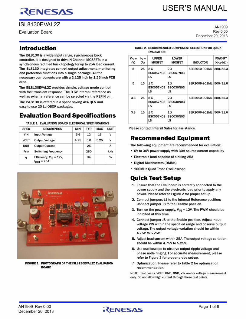
Quick Test Setup1. Ensure that the Eval board is correctly connected to the
power supply and the electronic load prior to apply any power. Please refer to Figure 2 for proper set-up.
2. Connect jumpers J1 to the Internal Reference position; Connect jumper J8 to the Disable position.
3. Turn on the power supply, VIN = 12V. The PWM should be inhibited at this time.
4. Connect jumper J8 to the Enable position. Adjust input voltage VIN within the specified range and observe output voltage. The output voltage variation should be within 4.75V to 5.25V.
5. Adjust load current within 25A. The output voltage variation should be within 4.75V to 5.25V.
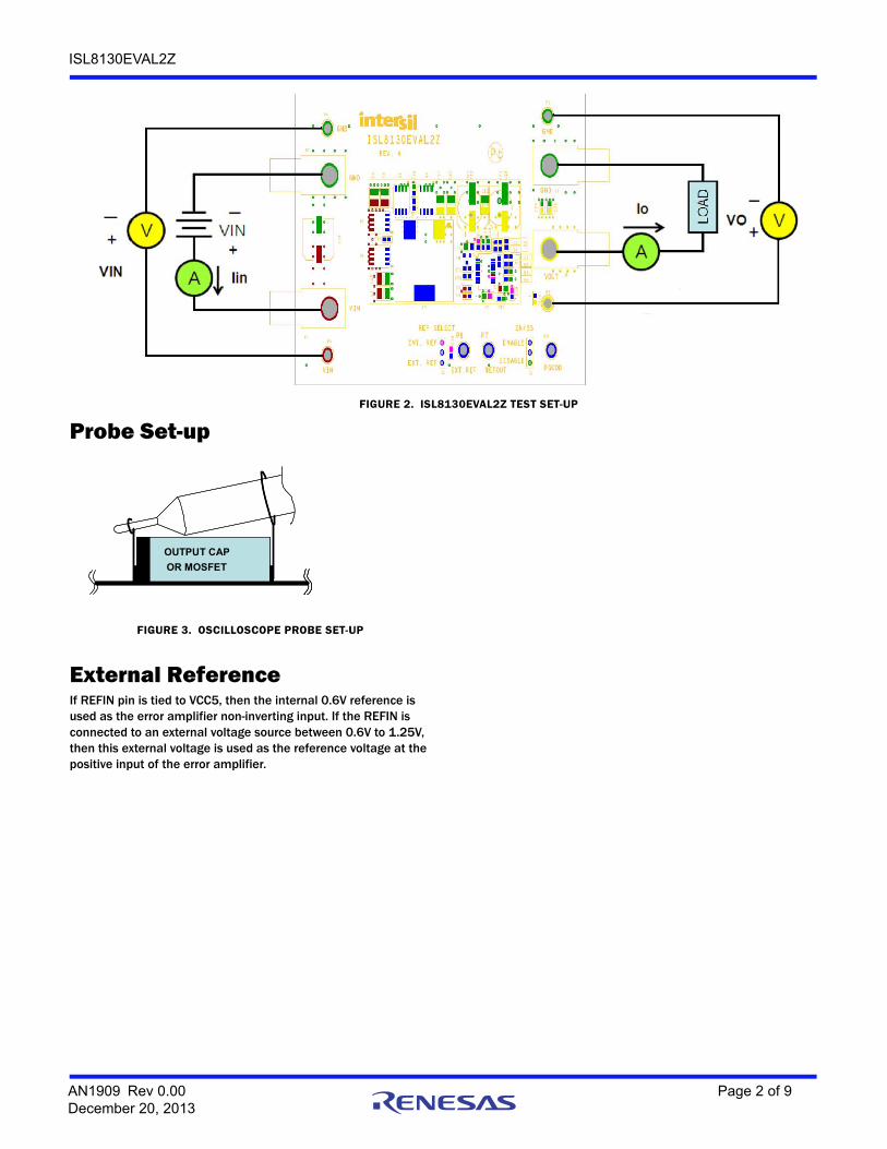
6. Use oscilloscope to observe output ripple voltage and phase node ringing. For accurate measurement, please refer to Figure 3 for proper probe set-up.
7. Optimization. Please refer to Table 2 for optimization recommendation.
NOTE: Test points: VOUT, GND, GND, VIN are for voltage measurement only. Do not allow high current through these test points.
TABLE 1. EVALUATION BOARD ELECTRICAL SPECIFICATIONS
SPEC DESCRIPTION MIN TYP MAX UNIT
VIN Input Voltage 5.6 12 16 V
VOUT Output Voltage 4.75 5.0 5.25 V
IOUT Output Current 25 A
Fsw Switching Frequency 280 kHz
Efficiency, VIN = 12V, IOUT = 25A
94 %
FIGURE 1. PHOTOGRAPH OF THE ISL8130EVAL2Z EVALUATION BOARD
TABLE 2. RECOMMENDED COMPONENT SELECTION FOR QUICK EVALUATION
VOUT(V)
IOUT(A)
UPPER MOSFET
LOWER MOSFET INDUCTOR
FSW/RT(kHz/k)
5 25 2 X BSC057N03 LS
2 X BSC057N03 LS
SER2010-901ML 280/52.3
5 15 1 X BSC057N03 LS
1 X BSC030N03 LS
SER2009-901ML 500/31.6
3.3 25 2 X BSC057N03 LS
2 X BSC030N03 LS
SER2010-901ML 280/52.3
3.3 15 1 X BSC057N03 LS
1 X BSC030N03 LS
SER2009-901ML 500/31.6
Please contact Intersil Sales for assistance.
AN1909 Rev 0.00 Page 1 of 9December 20, 2013
ISL8130EVAL2Z
Probe Set-up
External ReferenceIf REFIN pin is tied to VCC5, then the internal 0.6V reference is used as the error amplifier non-inverting input. If the REFIN is connected to an external voltage source between 0.6V to 1.25V, then this external voltage is used as the reference voltage at the positive input of the error amplifier.
FIGURE 2. ISL8130EVAL2Z TEST SET-UP
FIGURE 3. OSCILLOSCOPE PROBE SET-UP
OUTPUT CAP OR MOSFET OUTPUT CAP OR MOSFET OUTPUT CAP
OR MOSFET
AN1909 Rev 0.00 Page 2 of 9December 20, 2013
ISL8130EVAL2Z
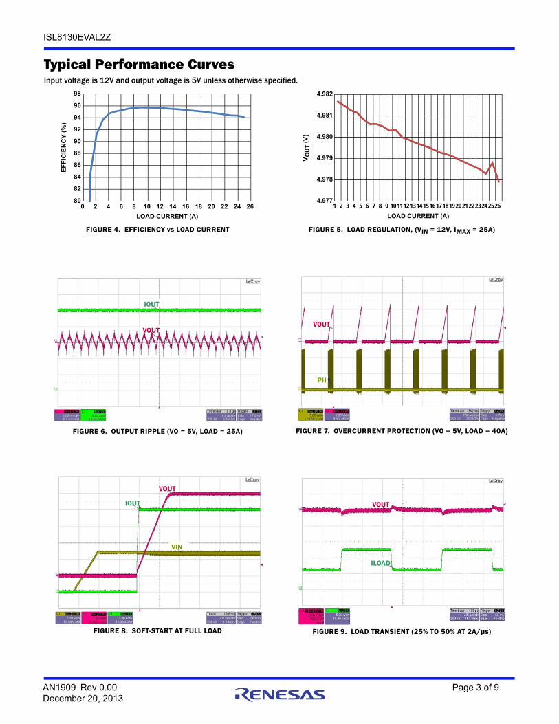
Typical Performance CurvesInput voltage is 12V and output voltage is 5V unless otherwise specified.
FIGURE 4. EFFICIENCY vs LOAD CURRENT FIGURE 5. LOAD REGULATION, (VIN = 12V, IMAX = 25A)
FIGURE 6. OUTPUT RIPPLE (VO = 5V, LOAD = 25A) FIGURE 7. OVERCURRENT PROTECTION (VO = 5V, LOAD = 40A)
FIGURE 8. SOFT-START AT FULL LOAD FIGURE 9. LOAD TRANSIENT (25% TO 50% AT 2A/µs)
80
82
84
86
88
90
92
94
96
98
0 2 4 6 8 10 12 14 16 18 20 22 24 26
LOAD CURRENT (A)
EF
FIC
IEN
CY
(%
)
4.977
4.978
4.979
4.980
4.981
4.982
1 2 3 4 5 6 7 8 9 10
VO
UT (
V)
11 12 13 14 15 16 17 18 19 20 21 22 23 24 25 26
LOAD CURRENT (A)
VOUT
IOUT
VOUT
PH
VOUT
IOUT
VIN
VOUT
ILOAD
AN1909 Rev 0.00 Page 3 of 9December 20, 2013

ISL8130EVAL2Z
ISL8130EVAL2Z Schematic
COMP
C160. 1uF
12
C 1710uF
12
P9
PGOOD
1
C3
470pF
12
VOU T
VI N
CD
EL
C100. 47uF
12
J 4
VI N
1
PGO
OD
R17
1
12
RPG
100K
12
VC C5
C 30
D NP
12 C 33
D NP
12
C 24
D NP
12 C26
DNP
12
L1 0. 9uH12
3
C 810uF
12
C 122. 2uF
12
R9
1. 2
12
C19
1000pF
12
VCC 5
C23
180uF
12PVC C
C 130. 1uF
12
R14 01 2
Q1
BSC 057N03LS
Q2BSC 057N03LS
UGATE
R 552. 3K
12
C 2722u
12
C 910uF
12
U 1
is l8130
VI N14
PGOOD20
ENSS19
I SEN8
REFI N9
R EFOUT11
N C12
CD EL1
R T16
SGN D15
PVC C4
VCC 513
OC SET10
BOOT7
UGATE6
PHASE5
LGATE3
PGN D2
C OMP18
FB17
C281uF
12
C 2100pF
12 C 291uF
12
J81
2
3
C3122u
12FB
EN SS
R230.1K 12
PHASE
C11. 5nF
12
Q3
BSC057N 03LS P3
VOU T
1
C 32D NP
12
R 4
16. 5K
12
VIN
RE
FOU
T
P7
REFOUT
1
Q4
BSC 057N03LS
REFI N
C15DN P
12
N 16246185
C410uF
12
C2010uF
12
P4
GN D
1
J1
1
2
3
PHASE
C 710uF
12
E N/ SS
P8
Ext . REF
1
C11 0. 22uF1 2
VC C5
R10
100K
12
INT.
REF
EXT
. REF
D IS AB LE
E NA BL E
R11
01 2
P5
GND
1
P6
1
J 5
GND
1
J6
VOU T
1
J7
GN D
1
C25
180uF
12
C 18
470uF
12
R1
121K1 2
D2
BAT54C-V-G
13
2
C61000pF
12
R81. 21K
12
R T
R1851K
12
R31k
1 2
AN1909 Rev 0.00 Page 4 of 9December 20, 2013

ISL8130EVAL2Z
TABLE 3. ISL8130EVAL2Z BILL OF MATERIALS
ITEM QTY PART REFERENCE VALUE DESCRIPTION PART NUMBER MANUFACTURER
ESSENTIAL COMPONENTS
1 1 C3 470pF Ceramic CAP, NP0 or C0G, sm0603 GENERIC GENERIC
2 2 C13, C16 0.1µF Ceramic CAP, X5R, 50V, sm0603 GENERIC GENERIC
3 2 C4, C17 10µF Ceramic CAP, X5R, 10V, sm0805 GENERIC GENERIC
4 1 C10 0.47µF Ceramic CAP, X5R, 16V, sm0603 GENERIC GENERIC
5 3 C27, C31 22µF Ceramic CAP, X5R, 25V, sm1210 GENERIC GENERIC
6 1 C12 2.2µF Ceramic CAP, X5R, 16V, sm0603 GENERIC GENERIC
7 2 C6, C19 1000pF Ceramic CAP, NP0 or C0G, sm0603 GENERIC GENERIC
8 2 C23, C25 180µF OSCON, 16V, Radial 8x9 16SEPC180MX SANYO
9 4 C7, C8, C9, C20 10µF Ceramic CAP, X5R, 25V, sm1210 GENERIC GENERIC
10 1 C2 100pF Ceramic CAP, NP0 or C0G, sm0603 GENERIC GENERIC
11 2 C28, C29 1µF Ceramic CAP, X5R, 25V,sm0603 GENERIC GENERIC
12 1 C1 1500pF Ceramic CAP, NP0 or C0G, sm0603 GENERIC GENERIC
13 1 C11 0.22µF Ceramic CAP, X5R, 16V,sm0603 GENERIC GENERIC
14 1 C18 470µF Alum. Cap, 50V 16SVPE470M SANYO
15 1 D2 Schottky Diode, 30V, SOT23 BAT54C Fairchild
16 1 L1 0.9µH Inductor SER2010-901ML Coilcraft
17 4 Q1, Q2, Q3, Q4 Single Channel NFET, 30V BSC057N03LS G Infineon
18 1 R5 52.3k Resistor, sm0603, 1% GENERIC GENERIC
19 1 R9 1.2 Resistor, sm0603, 10% GENERIC GENERIC
20 1 R2 30.1k Resistor, sm0603, 1% GENERIC GENERIC
21 2 R11, R14 0 Resistor, sm0603, 10% GENERIC GENERIC
22 1 R4 16.5k Resistor, sm0603, 1% GENERIC GENERIC
23 1 R17 1 Resistor, sm0603, 10% GENERIC GENERIC
24 1 R18 51k Resistor, sm0603, 1% GENERIC GENERIC
25 1 R1 121k Resistor, sm0603, 1% GENERIC GENERIC
26 1 R8 1.21k Resistor, sm0603, 1% GENERIC GENERIC
27 1 R3 1k Resistor, sm0603, 1% GENERIC GENERIC
28 2 R10, RPG 100k Resistor, sm0603, 1% GENERIC GENERIC
29 1 U1 PWM CONTROLLER, 20 Ld QSOP ISL8130IAZ INTERSIL
OPTIONAL COMPONENTS
30 6 C15, C24, C26, C30, C32, C33
DO NOT POPULATE
EVALUATION HARDWARE
31 4 J4, J5, J6, J7 HARDWARE, MTG, CABLE TERMINAL, 6-14AWG, LUG&SCRE , ROHS
KPA8CTP BERG/FCI
32 2 J1, J8 1x3 Header GENERIC GENERIC
33 7 P3, P4, P5, P6, P7, P8, P9 Test Points 1514-2 Keystone
AN1909 Rev 0.00 Page 5 of 9December 20, 2013
ISL8130EVAL2Z
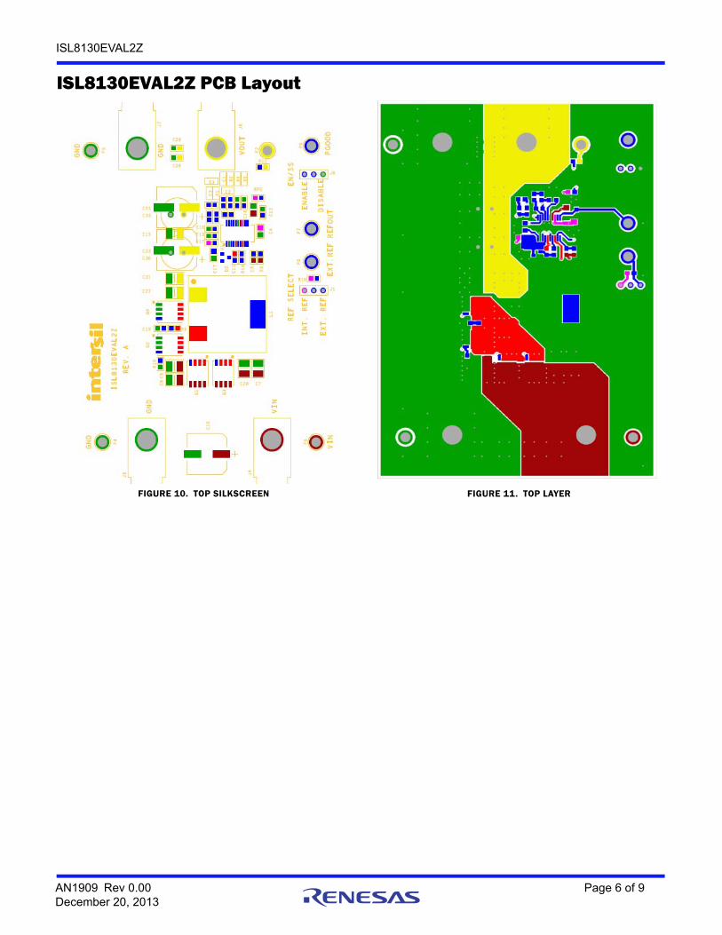
ISL8130EVAL2Z PCB Layout
FIGURE 10. TOP SILKSCREEN FIGURE 11. TOP LAYER
AN1909 Rev 0.00 Page 6 of 9December 20, 2013
ISL8130EVAL2Z
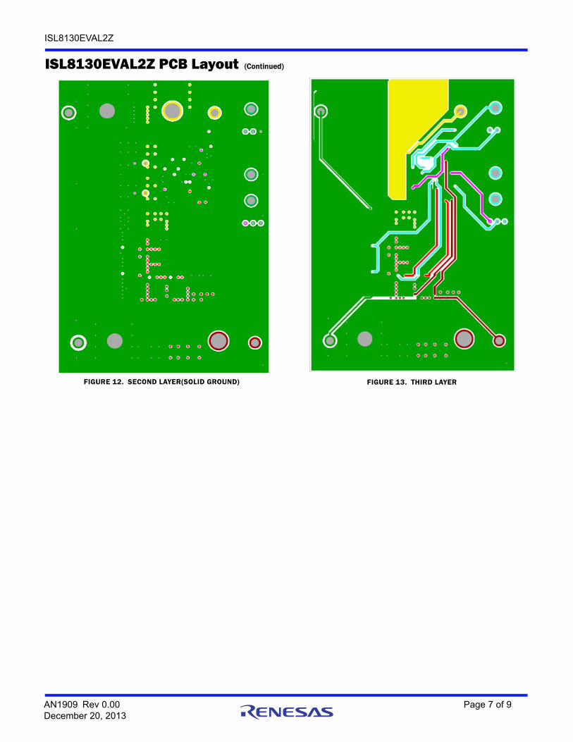
FIGURE 12. SECOND LAYER(SOLID GROUND) FIGURE 13. THIRD LAYER
ISL8130EVAL2Z PCB Layout (Continued)
AN1909 Rev 0.00 Page 7 of 9December 20, 2013

ISL8130EVAL2Z
FIGURE 14. BOTTOM LAYER FIGURE 15. BOTTOM SILKSCREEN
ISL8130EVAL2Z PCB Layout (Continued)
AN1909 Rev 0.00 Page 8 of 9December 20, 2013
http://www.renesas.comRefer to "http://www.renesas.com/" for the latest and detailed information.
Renesas Electronics America Inc.1001 Murphy Ranch Road, Milpitas, CA 95035, U.S.A.Tel: +1-408-432-8888, Fax: +1-408-434-5351Renesas Electronics Canada Limited9251 Yonge Street, Suite 8309 Richmond Hill, Ontario Canada L4C 9T3Tel: +1-905-237-2004Renesas Electronics Europe LimitedDukes Meadow, Millboard Road, Bourne End, Buckinghamshire, SL8 5FH, U.KTel: +44-1628-651-700, Fax: +44-1628-651-804Renesas Electronics Europe GmbHArcadiastrasse 10, 40472 Düsseldorf, Germany Tel: +49-211-6503-0, Fax: +49-211-6503-1327Renesas Electronics (China) Co., Ltd.Room 1709 Quantum Plaza, No.27 ZhichunLu, Haidian District, Beijing, 100191 P. R. ChinaTel: +86-10-8235-1155, Fax: +86-10-8235-7679Renesas Electronics (Shanghai) Co., Ltd.Unit 301, Tower A, Central Towers, 555 Langao Road, Putuo District, Shanghai, 200333 P. R. China Tel: +86-21-2226-0888, Fax: +86-21-2226-0999Renesas Electronics Hong Kong LimitedUnit 1601-1611, 16/F., Tower 2, Grand Century Place, 193 Prince Edward Road West, Mongkok, Kowloon, Hong KongTel: +852-2265-6688, Fax: +852 2886-9022Renesas Electronics Taiwan Co., Ltd.13F, No. 363, Fu Shing North Road, Taipei 10543, TaiwanTel: +886-2-8175-9600, Fax: +886 2-8175-9670Renesas Electronics Singapore Pte. Ltd.80 Bendemeer Road, Unit #06-02 Hyflux Innovation Centre, Singapore 339949Tel: +65-6213-0200, Fax: +65-6213-0300Renesas Electronics Malaysia Sdn.Bhd.Unit 1207, Block B, Menara Amcorp, Amcorp Trade Centre, No. 18, Jln Persiaran Barat, 46050 Petaling Jaya, Selangor Darul Ehsan, MalaysiaTel: +60-3-7955-9390, Fax: +60-3-7955-9510Renesas Electronics India Pvt. Ltd.No.777C, 100 Feet Road, HAL 2nd Stage, Indiranagar, Bangalore 560 038, IndiaTel: +91-80-67208700, Fax: +91-80-67208777Renesas Electronics Korea Co., Ltd.17F, KAMCO Yangjae Tower, 262, Gangnam-daero, Gangnam-gu, Seoul, 06265 KoreaTel: +82-2-558-3737, Fax: +82-2-558-5338
SALES OFFICES
© 2018 Renesas Electronics Corporation. All rights reserved.Colophon 7.0
(Rev.4.0-1 November 2017)
Notice
1. Descriptions of circuits, software and other related information in this document are provided only to illustrate the operation of semiconductor products and application examples. You are fully responsible for
the incorporation or any other use of the circuits, software, and information in the design of your product or system. Renesas Electronics disclaims any and all liability for any losses and damages incurred by
you or third parties arising from the use of these circuits, software, or information.
2. Renesas Electronics hereby expressly disclaims any warranties against and liability for infringement or any other claims involving patents, copyrights, or other intellectual property rights of third parties, by or
arising from the use of Renesas Electronics products or technical information described in this document, including but not limited to, the product data, drawings, charts, programs, algorithms, and application
examples.
3. No license, express, implied or otherwise, is granted hereby under any patents, copyrights or other intellectual property rights of Renesas Electronics or others.
4. You shall not alter, modify, copy, or reverse engineer any Renesas Electronics product, whether in whole or in part. Renesas Electronics disclaims any and all liability for any losses or damages incurred by
you or third parties arising from such alteration, modification, copying or reverse engineering.
5. Renesas Electronics products are classified according to the following two quality grades: “Standard” and “High Quality”. The intended applications for each Renesas Electronics product depends on the
product’s quality grade, as indicated below.
"Standard": Computers; office equipment; communications equipment; test and measurement equipment; audio and visual equipment; home electronic appliances; machine tools; personal electronic
equipment; industrial robots; etc.
"High Quality": Transportation equipment (automobiles, trains, ships, etc.); traffic control (traffic lights); large-scale communication equipment; key financial terminal systems; safety control equipment; etc.
Unless expressly designated as a high reliability product or a product for harsh environments in a Renesas Electronics data sheet or other Renesas Electronics document, Renesas Electronics products are
not intended or authorized for use in products or systems that may pose a direct threat to human life or bodily injury (artificial life support devices or systems; surgical implantations; etc.), or may cause
serious property damage (space system; undersea repeaters; nuclear power control systems; aircraft control systems; key plant systems; military equipment; etc.). Renesas Electronics disclaims any and all
liability for any damages or losses incurred by you or any third parties arising from the use of any Renesas Electronics product that is inconsistent with any Renesas Electronics data sheet, user’s manual or
other Renesas Electronics document.
6. When using Renesas Electronics products, refer to the latest product information (data sheets, user’s manuals, application notes, “General Notes for Handling and Using Semiconductor Devices” in the
reliability handbook, etc.), and ensure that usage conditions are within the ranges specified by Renesas Electronics with respect to maximum ratings, operating power supply voltage range, heat dissipation
characteristics, installation, etc. Renesas Electronics disclaims any and all liability for any malfunctions, failure or accident arising out of the use of Renesas Electronics products outside of such specified
ranges.
7. Although Renesas Electronics endeavors to improve the quality and reliability of Renesas Electronics products, semiconductor products have specific characteristics, such as the occurrence of failure at a
certain rate and malfunctions under certain use conditions. Unless designated as a high reliability product or a product for harsh environments in a Renesas Electronics data sheet or other Renesas
Electronics document, Renesas Electronics products are not subject to radiation resistance design. You are responsible for implementing safety measures to guard against the possibility of bodily injury, injury
or damage caused by fire, and/or danger to the public in the event of a failure or malfunction of Renesas Electronics products, such as safety design for hardware and software, including but not limited to
redundancy, fire control and malfunction prevention, appropriate treatment for aging degradation or any other appropriate measures. Because the evaluation of microcomputer software alone is very difficult
and impractical, you are responsible for evaluating the safety of the final products or systems manufactured by you.
8. Please contact a Renesas Electronics sales office for details as to environmental matters such as the environmental compatibility of each Renesas Electronics product. You are responsible for carefully and
sufficiently investigating applicable laws and regulations that regulate the inclusion or use of controlled substances, including without limitation, the EU RoHS Directive, and using Renesas Electronics
products in compliance with all these applicable laws and regulations. Renesas Electronics disclaims any and all liability for damages or losses occurring as a result of your noncompliance with applicable
laws and regulations.
9. Renesas Electronics products and technologies shall not be used for or incorporated into any products or systems whose manufacture, use, or sale is prohibited under any applicable domestic or foreign laws
or regulations. You shall comply with any applicable export control laws and regulations promulgated and administered by the governments of any countries asserting jurisdiction over the parties or
transactions.
10. It is the responsibility of the buyer or distributor of Renesas Electronics products, or any other party who distributes, disposes of, or otherwise sells or transfers the product to a third party, to notify such third
party in advance of the contents and conditions set forth in this document.
11. This document shall not be reprinted, reproduced or duplicated in any form, in whole or in part, without prior written consent of Renesas Electronics.
12. Please contact a Renesas Electronics sales office if you have any questions regarding the information contained in this document or Renesas Electronics products.
(Note 1) “Renesas Electronics” as used in this document means Renesas Electronics Corporation and also includes its directly or indirectly controlled subsidiaries.
(Note 2) “Renesas Electronics product(s)” means any product developed or manufactured by or for Renesas Electronics.
Related Documents