FN7627 Rev 0.00 Page 1 of 18 July 2, 2010 FN7627 Rev 0.00 July 2, 2010 ISL54225 High-Speed USB 2.0 (480Mbps) Multiplexer with Overvoltage Protection (OVP) DATASHEET The ISL54225 is a single supply dual 2:1 multiplexer that can operate from a single 2.7V to 5.25V supply. It contains two SPDT (Single Pole/Double Throw) switches configured as a DPDT. The part was designed for switching or routing of USB High-Speed signals and/or USB Full-speed signals in portable battery powered products. The 6.5 switches were specifically designed to pass USB high speed/full speed data signals. They have high bandwidth and low capacitance to pass USB high speed data signals with minimal DISTORTION. The ISL54225 has OVP circuitry on the D-/D+ COM pins that opens the USB in-line switches when the voltage at these pins exceeds 3.8V (typ) or goes negative by -0.5V (typ). It isolates fault voltages up to +5.25V or down to -5V from getting passed to the other-side of the switch, thereby protecting the USB transceivers. The digital logic inputs are 1.8V logic compatible when operated with a 2.7V to 3.6V supply. The ISL54225 has an output enable pin to open all the switches. It can be used to facilitate proper bus disconnect and connection when switching between the USB sources. The ISL54225 is available in 10 Ld 1.8mmx1.4mm μTQFN and 10 Ld TDFN packages. It operates over a temperature range of -40°C to +85°C. Features • High-Speed (480Mbps) and Full-Speed (12Mbps) Signaling Capability per USB 2.0 • 1.8V Logic Compatible (2.7V to +3.6V Supply) • Enable Pin to Open all Switches • Low Power Mode • Power OFF Protection • D-/D+ Pins Overvoltage Protection for +5.25V and -5V Fault Voltages • -3dB Frequency 780MHz • Low ON Capacitance @ 240MHz 3.3pF • Low ON-Resistance 6.5 • Single Supply Operation (V DD ) 2.7V to 5.25V • Available in μTQFN and TDFN Packages • Pb-Free (RoHS Compliant) • Compliant with USB 2.0 Short Circuit and Overvoltage Requirements Without Additional External Components Applications*(see page 16) • MP3 and other Personal Media Players • Cellular/Mobile Phones • PDAs • Digital Cameras and Camcorders • USB Switching Typical Application USB 2.0 HS Eye Pattern With Switches in the Signal Path ISL54225 USB TRANSCEIVER USB CONNECTOR D- D+ GND HSD1+ HSD1- VDD OE μP VBUS D- D+ GND OVP 500Ω SEL LOGIC CONTROL 3.3V USB TRANSCEIVER HSD2+ HSD2- TIME SCALE (0.2ns/DIV) VOLTAGE SCALE (0.1V/DIV)

Welcome message from author
This document is posted to help you gain knowledge. Please leave a comment to let me know what you think about it! Share it to your friends and learn new things together.
Transcript

FN7627Rev 0.00
July 2, 2010
ISL54225High-Speed USB 2.0 (480Mbps) Multiplexer with Overvoltage Protection (OVP)
DATASHEET
The ISL54225 is a single supply dual 2:1 multiplexer that can operate from a single 2.7V to 5.25V supply. It contains two SPDT (Single Pole/Double Throw) switches configured as a DPDT. The part was designed for switching or routing of USB High-Speed signals and/or USB Full-speed signals in portable battery powered products.
The 6.5switches were specifically designed to pass USB high speed/full speed data signals. They have high bandwidth and low capacitance to pass USB high speed data signals with minimal DISTORTION.
The ISL54225 has OVP circuitry on the D-/D+ COM pins that opens the USB in-line switches when the voltage at these pins exceeds 3.8V (typ) or goes negative by -0.5V (typ). It isolates fault voltages up to +5.25V or down to -5V from getting passed to the other-side of the switch, thereby protecting the USB transceivers.
The digital logic inputs are 1.8V logic compatible when operated with a 2.7V to 3.6V supply. The ISL54225 has an output enable pin to open all the switches. It can be used to facilitate proper bus disconnect and connection when switching between the USB sources.
The ISL54225 is available in 10 Ld 1.8mmx1.4mm µTQFN and 10 Ld TDFN packages. It operates over a temperature range of -40°C to +85°C.
Features• High-Speed (480Mbps) and Full-Speed (12Mbps)
Signaling Capability per USB 2.0• 1.8V Logic Compatible (2.7V to +3.6V Supply)• Enable Pin to Open all Switches• Low Power Mode• Power OFF Protection• D-/D+ Pins Overvoltage Protection for +5.25V and
-5V Fault Voltages• -3dB Frequency 780MHz• Low ON Capacitance @ 240MHz 3.3pF• Low ON-Resistance 6.5• Single Supply Operation (VDD) 2.7V to 5.25V• Available in µTQFN and TDFN Packages• Pb-Free (RoHS Compliant)• Compliant with USB 2.0 Short Circuit and
Overvoltage Requirements Without Additional External Components
Applications*(see page 16)• MP3 and other Personal Media Players• Cellular/Mobile Phones• PDAs• Digital Cameras and Camcorders• USB Switching
Typical Application USB 2.0 HS Eye Pattern With Switches in the Signal Path
ISL54225
USBTRANSCEIVER
US
B C
ON
NEC
TOR
D-
D+
GND
HSD1+
HSD1-
VDDOE
µPVBUS
D-
D+
GND
OVP
500Ω
SELLOGIC
CONTROL
3.3V
USBTRANSCEIVERHSD2+
HSD2-
TIME SCALE (0.2ns/DIV)
VO
LTA
GE
SC
ALE
(0
.1V
/DIV
)
FN7627 Rev 0.00 Page 1 of 18July 2, 2010
ISL54225
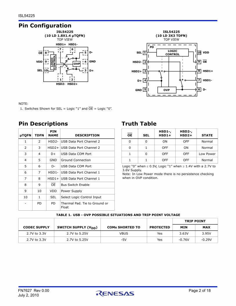
Pin ConfigurationISL54225
(10 LD 1.8X1.4 µTQFN)TOP VIEW
ISL54225(10 LD 3X3 TDFN)
TOP VIEW
NOTE:1. Switches Shown for SEL = Logic “1” and OE = Logic “0”.
8
10
D-OE
D+
VDD 9
7
2
3
4 GND
HSD2- HSD2+
5
SEL
LOG
ICC
ON
TRO
L
1
6
HSD1+ HSD1-
OVP
SEL
HSD2-
D+
HSD2+ HSD1+
GND
1
2
3
4
5
10
9
8
7
6 D-
HSD1-
VDD
OE
LOGICCONTROL
OVP
PD
Pin Descriptions
µTQFN TDFNPIN
NAME DESCRIPTION
1 2 HSD2- USB Data Port Channel 2
2 3 HSD2+ USB Data Port Channel 2
3 4 D+ USB Data COM Port
4 5 GND Ground Connection
5 6 D- USB Data COM Port
6 7 HSD1- USB Data Port Channel 1
7 8 HSD1+ USB Data Port Channel 1
8 9 OE Bus Switch Enable
9 10 VDD Power Supply
10 1 SEL Select Logic Control Input
- PD PD Thermal Pad. Tie to Ground or Float
Truth Table
OE SELHSD1-, HSD1+
HSD2-, HSD2+ STATE
0 0 ON OFF Normal
0 1 OFF ON Normal
1 0 OFF OFF Low Power
1 1 OFF OFF Normal
Logic “0” when 0.5V, Logic “1” when 1.4V with a 2.7V to 3.6V Supply.Note: In Low Power mode there is no persistence checking when in OVP condition.
TABLE 1. USB - OVP POSSIBLE SITUATIONS AND TRIP POINT VOLTAGE
CODEC SUPPLY SWITCH SUPPLY (VDD) COMs SHORTED TO PROTECTED
TRIP POINT
MIN MAX
2.7V to 3.3V 2.7V to 5.25V VBUS Yes 3.63V 3.95V
2.7V to 3.3V 2.7V to 5.25V -5V Yes -0.76V -0.29V
FN7627 Rev 0.00 Page 2 of 18July 2, 2010
ISL54225
Ordering InformationPART
NUMBERPART
MARKINGTEMP. RANGE
(°C)PACKAGE(Pb-Free)
PKG.DWG. #
ISL54225IRUZ-T (Notes 2, 3) U0 -40 to +85 10 Ld 1.8x1.4mm µTQFN (Tape and Reel) L10.1.8x1.4A
ISL54225IRUZ-T7A (Notes 2, 3) U0 -40 to +85 10 Ld 1.8x1.4mm µTQFN (Tape and Reel) L10.1.8x1.4A
ISL54225IRTZ (Note 4) 4225 -40 to +85 10 Ld 3x3 TDFN L10.3x3A
ISL54225IRTZ-T (Notes 2, 4) 4225 -40 to +85 10 Ld 3x3 TDFN (Tape and Reel) L10.3x3A
ISL54225IRTZEVAL1Z Evaluation Board
NOTES:2. Please refer to TB347 for details on reel specifications.3. These Intersil Pb-free plastic packaged products employ special Pb-free material sets; molding compounds/die attach materials
and NiPdAu plate - e4 termination finish, which is RoHS compliant and compatible with both SnPb and Pb-free soldering operations. Intersil Pb-free products are MSL classified at Pb-free peak reflow temperatures that meet or exceed the Pb-free requirements of IPC/JEDEC J STD-020.
4. These Intersil Pb-free plastic packaged products employ special Pb-free material sets, molding compounds/die attach materials, and 100% matte tin plate plus anneal (e3 termination finish, which is RoHS compliant and compatible with both SnPb and Pb-free soldering operations). Intersil Pb-free products are MSL classified at Pb-free peak reflow temperatures that meet or exceed the Pb-free requirements of IPC/JEDEC J STD-020.
5. For Moisture Sensitivity Level (MSL), please see device information page for ISL54225. For more information on MSL please see techbrief TB363.
FN7627 Rev 0.00 Page 3 of 18July 2, 2010

ISL54225
Absolute Maximum Ratings Thermal InformationVDD to GND . . . . . . . . . . . . . . . . . . . . . . . . -0.3V to 6.5VVDD to Dx . . . . . . . . . . . . . . . . . . . . . . . . . . . . . . . . 10.5VDx to HSD1x, HSD2x . . . . . . . . . . . . . . . . . . . . . . . . .8.6VInput Voltages
HSD2x, HSD1x . . . . . . . . . . . . . . . . . . . . . - 0.3V to 6.5VSEL, OE . . . . . . . . . . . . . . . . . . . . . . . . . . -0.3V to 6.5V
Output VoltagesD+, D- . . . . . . . . . . . . . . . . . . . . . . . . . . . . . -5V to 6.5V
Continuous Current (HSD2x, HSD1x) . . . . . . . . . . . .±40mAPeak Current (HSD2x, HSD1x)
(Pulsed 1ms, 10% Duty Cycle, Max) . . . . . . . . . . ±100mAESD Rating: Human Body Model (Tested per JESD22-A114-F) . . .>5.5kV Machine Model (Tested per JESD22-A115-A). . . . . . . >250V Charged Device Model (Tested per JESD22-C101-D) . . >2kVLatch-up Tested per JEDEC; Class II Level A . . . . . at +85°C
Thermal Resistance (Typical) JA (°C/W) JC (°C/W)10 Ld µTQFN Package (Note 6, 7) . 210 16510 Ld TDFN Package (Notes 8, 9). . 58 22
Maximum Junction Temperature (Plastic Package). . +150°CMaximum Storage Temperature Range . . . -65°C to +150°CPb-Free Reflow Profile . . . . . . . . . . . . . . . . . .see link below
http://www.intersil.com/pbfree/Pb-FreeReflow.asp
Recommended Operating ConditionsTemperature Range . . . . . . . . . . . . . . . . . . -40°C to +85°CVDD Supply Voltage Range . . . . . . . . . . . . . . 2.7V to 5.25VLogic Control Input Voltage . . . . . . . . . . . . . . . 0V to 5.25VAnalog Signal Range
VDD = 2.7V to 5.25V . . . . . . . . . . . . . . . . . . . 0V to 3.6V
CAUTION: Do not operate at or near the maximum ratings listed for extended periods of time. Exposure to such conditions may adversely impactproduct reliability and result in failures not covered by warranty.
NOTES:6. JA is measured with the component mounted on a high effective thermal conductivity test board in free air. See Tech Brief
TB379 for details.7. For JC, the “case temp” location is taken at the package top center.8. JA is measured in free air with the component mounted on a high effective thermal conductivity test board with “direct attach”
features. See Tech Brief TB379.9. For JC, the “case temp” location is the center of the exposed metal pad on the package underside.
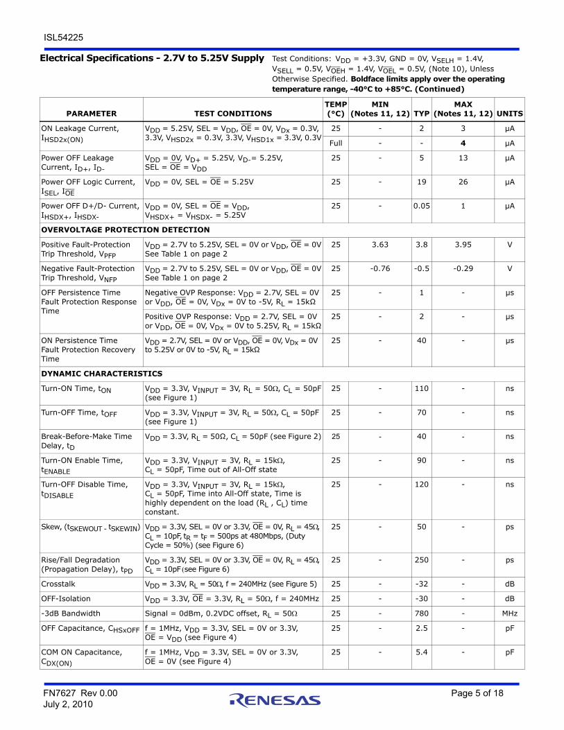
Electrical Specifications - 2.7V to 5.25V Supply Test Conditions: VDD = +3.3V, GND = 0V, VSELH = 1.4V, VSELL = 0.5V, VOEH = 1.4V, VOEL = 0.5V, (Note 10), Unless Otherwise Specified. Boldface limits apply over the operating temperature range, -40°C to +85°C.
PARAMETER TEST CONDITIONSTEMP(°C)
MIN(Notes 11, 12) TYP
MAX(Notes 11, 12) UNITS
ANALOG SWITCH CHARACTERISTICS
ON-Resistance, rON (High-Speed)
VDD = 2.7V, SEL = 0.5V or 1.4V, OE = 0.5V, IDx = 17mA, VHSD1x or VHSD2x = 0V to 400mV (see Figure 3, Note 15)
25 - 6.5 8
Full - - 10
rON Matching Between Channels, rON (High-Speed)
VDD = 2.7V, SEL = 0.5V or 1.4V, OE = 0.5V, IDx = 17mA, VHSD1x or VHSD2x = Voltage at max rON, (Notes 14, 15)
25 - 0.2 0.45
Full - - 0.5
rON Flatness, RFLAT(ON) (High-Speed)
VDD = 2.7V, SEL = 0.5V or 1.4V, OE = 0.5V, IDx = 17mA, VHSD1x or VHSD2x = 0V to 400mV, (Notes 13, 15)
25 - 0.3 0.5
Full - - 1
ON-Resistance, rON VDD = 3.3V, SEL = 0.5V or 1.4V, OE = 0.5V, ICOMx = 17mA, VD+ or VD-= 3.3V (See Figure 4, Note 15)
25 - 12 20
Full - - 25
OFF Leakage Current, IHSD1x(OFF)
VDD = 5.25V, SEL = VDD and OE = VDD orOE = 0V, VDx = 0.3V, 3.3V, VHSD1x = 3.3V, 0.3V, VHSD2x = 0.3V, 3.3V
25 -20 1 20 nA
Full - 30 - nA
ON Leakage Current, IHSD1x(ON)
VDD = 5.25V, SEL = OE = 0V, VDx = 0.3V, 3.3V, VHSD1X = 0.3V, 3.3V, VHSD2x = 3.3V, 0.3V
25 - 2 3 µA
Full - - 4 µA
OFF Leakage Current, IHSD2x(OFF)
VDD = 5.25V, SEL = OE = 0V or OE = VDD, VDx = 3.3V, 0.3V, VHSD2x = 0.3V, 3.3V, VHSD1X = 3.3V, 0.3V
25 -20 1 20 nA
Full - 30 - nA
FN7627 Rev 0.00 Page 4 of 18July 2, 2010
ISL54225
ON Leakage Current, IHSD2x(ON)
VDD = 5.25V, SEL = VDD, OE = 0V, VDx = 0.3V, 3.3V, VHSD2x = 0.3V, 3.3V, VHSD1x = 3.3V, 0.3V
25 - 2 3 µA
Full - - 4 µA
Power OFF Leakage Current, ID+, ID-
VDD = 0V, VD+ = 5.25V, VD-= 5.25V, SEL = OE = VDD
25 - 5 13 µA
Power OFF Logic Current, ISEL, IOE
VDD = 0V, SEL = OE = 5.25V 25 - 19 26 µA
Power OFF D+/D- Current, IHSDX+, IHSDX-
VDD = 0V, SEL = OE = VDD, VHSDX+ = VHSDX- = 5.25V
25 - 0.05 1 µA
OVERVOLTAGE PROTECTION DETECTION
Positive Fault-Protection Trip Threshold, VPFP
VDD = 2.7V to 5.25V, SEL = 0V or VDD, OE = 0VSee Table 1 on page 2
25 3.63 3.8 3.95 V
Negative Fault-Protection Trip Threshold, VNFP
VDD = 2.7V to 5.25V, SEL = 0V or VDD, OE = 0VSee Table 1 on page 2
25 -0.76 -0.5 -0.29 V
OFF Persistence TimeFault Protection Response Time
Negative OVP Response: VDD = 2.7V, SEL = 0V or VDD, OE = 0V, VDx = 0V to -5V, RL = 15kΩ
25 - 1 - µs
Positive OVP Response: VDD = 2.7V, SEL = 0V or VDD, OE = 0V, VDx = 0V to 5.25V, RL = 15kΩ
25 - 2 - µs
ON Persistence TimeFault Protection Recovery Time
VDD = 2.7V, SEL = 0V or VDD, OE = 0V, VDx = 0V to 5.25V or 0V to -5V, RL = 15kΩ
25 - 40 - µs
DYNAMIC CHARACTERISTICS
Turn-ON Time, tON VDD = 3.3V, VINPUT = 3V, RL = 50, CL = 50pF(see Figure 1)
25 - 110 - ns
Turn-OFF Time, tOFF VDD = 3.3V, VINPUT = 3V, RL = 50, CL = 50pF (see Figure 1)
25 - 70 - ns
Break-Before-Make Time Delay, tD
VDD = 3.3V, RL = 50Ω, CL = 50pF (see Figure 2) 25 - 40 - ns
Turn-ON Enable Time, tENABLE
VDD = 3.3V, VINPUT = 3V, RL = 15k, CL = 50pF, Time out of All-Off state
25 - 90 - ns
Turn-OFF Disable Time, tDISABLE
VDD = 3.3V, VINPUT = 3V, RL = 15k, CL = 50pF, Time into All-Off state, Time is highly dependent on the load (RL , CL) time constant.
25 - 120 - ns
Skew, (tSKEWOUT - tSKEWIN) VDD = 3.3V, SEL = 0V or 3.3V, OE = 0V, RL = 45,CL = 10pF,tR = tF = 500ps at 480Mbps, (Duty Cycle = 50%) (see Figure 6)
25 - 50 - ps
Rise/Fall Degradation (Propagation Delay), tPD
VDD = 3.3V, SEL = 0V or 3.3V, OE = 0V, RL = 45,CL = 10pFsee Figure 6)
25 - 250 - ps
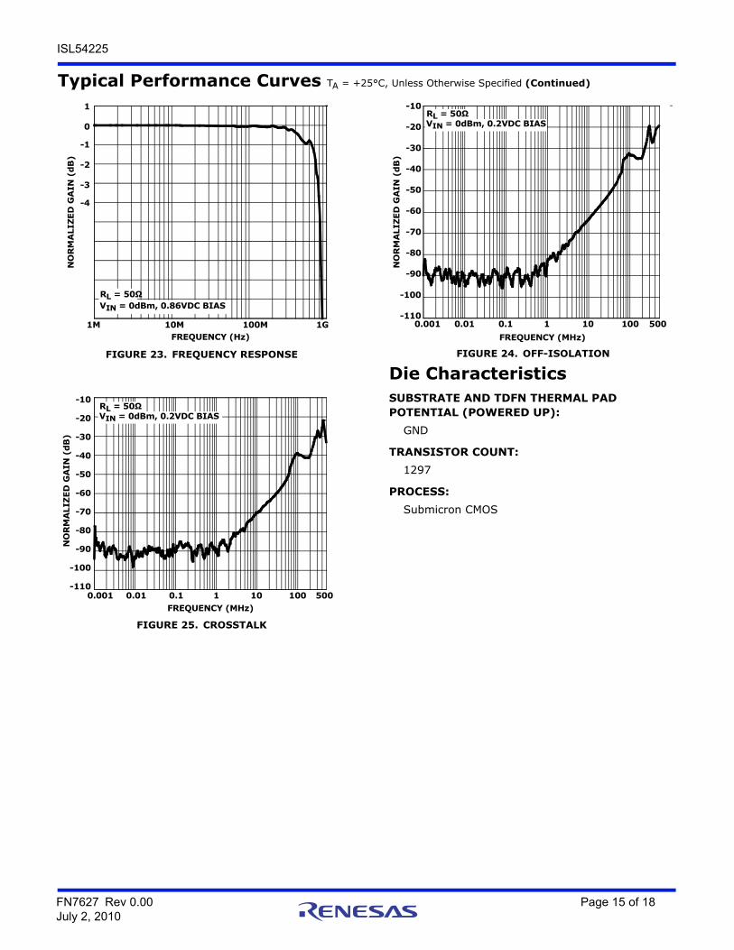
Crosstalk VDD = 3.3V, RL = 50, f = 240MHz (see Figure 5) 25 - -32 - dB
OFF-Isolation VDD = 3.3V, OE = 3.3V, RL = 50, f = 240MHz 25 - -30 - dB
-3dB Bandwidth Signal = 0dBm, 0.2VDC offset, RL = 50 25 - 780 - MHz
OFF Capacitance, CHSxOFF f = 1MHz, VDD = 3.3V, SEL = 0V or 3.3V,OE = VDD (see Figure 4)
25 - 2.5 - pF
COM ON Capacitance, CDX(ON)
f = 1MHz, VDD = 3.3V, SEL = 0V or 3.3V,OE = 0V (see Figure 4)
25 - 5.4 - pF
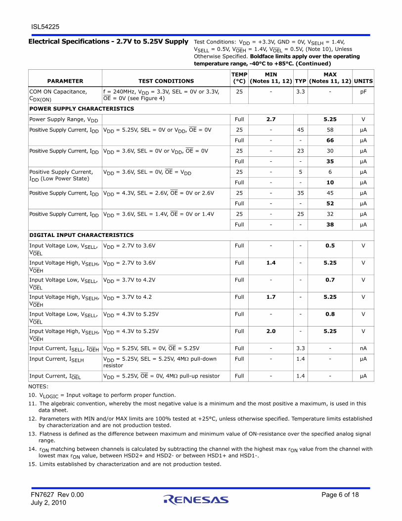
Electrical Specifications - 2.7V to 5.25V Supply Test Conditions: VDD = +3.3V, GND = 0V, VSELH = 1.4V, VSELL = 0.5V, VOEH = 1.4V, VOEL = 0.5V, (Note 10), Unless Otherwise Specified. Boldface limits apply over the operating temperature range, -40°C to +85°C. (Continued)
PARAMETER TEST CONDITIONSTEMP(°C)
MIN(Notes 11, 12) TYP
MAX(Notes 11, 12) UNITS
FN7627 Rev 0.00 Page 5 of 18July 2, 2010
ISL54225
COM ON Capacitance, CDX(ON)
f = 240MHz, VDD = 3.3V, SEL = 0V or 3.3V, OE = 0V (see Figure 4)
25 - 3.3 - pF
POWER SUPPLY CHARACTERISTICS
Power Supply Range, VDD Full 2.7 5.25 V
Positive Supply Current, IDD VDD = 5.25V, SEL = 0V or VDD, OE = 0V 25 - 45 58 µA
Full - - 66 µA
Positive Supply Current, IDD VDD = 3.6V, SEL = 0V or VDD, OE = 0V 25 - 23 30 µA
Full - - 35 µA
Positive Supply Current, IDD (Low Power State)
VDD = 3.6V, SEL = 0V, OE = VDD 25 - 5 6 µA
Full - - 10 µA
Positive Supply Current, IDD VDD = 4.3V, SEL = 2.6V, OE = 0V or 2.6V 25 - 35 45 µA
Full - - 52 µA
Positive Supply Current, IDD VDD = 3.6V, SEL = 1.4V, OE = 0V or 1.4V 25 - 25 32 µA
Full - - 38 µA
DIGITAL INPUT CHARACTERISTICS
Input Voltage Low, VSELL, VOEL
VDD = 2.7V to 3.6V Full - - 0.5 V
Input Voltage High, VSELH, VOEH
VDD = 2.7V to 3.6V Full 1.4 - 5.25 V
Input Voltage Low, VSELL, VOEL
VDD = 3.7V to 4.2V Full - - 0.7 V
Input Voltage High, VSELH, VOEH
VDD = 3.7V to 4.2 Full 1.7 - 5.25 V
Input Voltage Low, VSELL, VOEL
VDD = 4.3V to 5.25V Full - - 0.8 V
Input Voltage High, VSELH, VOEH
VDD = 4.3V to 5.25V Full 2.0 - 5.25 V
Input Current, ISELL, IOEH VDD = 5.25V, SEL = 0V, OE = 5.25V Full - 3.3 - nA
Input Current, ISELH VDD = 5.25V, SEL = 5.25V, 4M pull-down resistor
Full - 1.4 - µA
Input Current, IOEL VDD = 5.25V, OE = 0V, 4M pull-up resistor Full - 1.4 - µA
NOTES:10. VLOGIC = Input voltage to perform proper function.11. The algebraic convention, whereby the most negative value is a minimum and the most positive a maximum, is used in this
data sheet.12. Parameters with MIN and/or MAX limits are 100% tested at +25°C, unless otherwise specified. Temperature limits established
by characterization and are not production tested.13. Flatness is defined as the difference between maximum and minimum value of ON-resistance over the specified analog signal
range.14. rON matching between channels is calculated by subtracting the channel with the highest max rON value from the channel with
lowest max rON value, between HSD2+ and HSD2- or between HSD1+ and HSD1-.15. Limits established by characterization and are not production tested.
Electrical Specifications - 2.7V to 5.25V Supply Test Conditions: VDD = +3.3V, GND = 0V, VSELH = 1.4V, VSELL = 0.5V, VOEH = 1.4V, VOEL = 0.5V, (Note 10), Unless Otherwise Specified. Boldface limits apply over the operating temperature range, -40°C to +85°C. (Continued)
PARAMETER TEST CONDITIONSTEMP(°C)
MIN(Notes 11, 12) TYP
MAX(Notes 11, 12) UNITS
FN7627 Rev 0.00 Page 6 of 18July 2, 2010

ISL54225
Test Circuits and Waveforms
Logic input waveform is inverted for switches that have theopposite logic sense.
FIGURE 1A. MEASUREMENT POINTS
Repeat test for all switches. CL includes fixture and stray capacitance.
FIGURE 1B. TEST CIRCUIT
FIGURE 1. SWITCHING TIMES
FIGURE 2A. MEASUREMENT POINTS
Repeat test for all switches. CL includes fixture and stray capacitance.
FIGURE 2B. TEST CIRCUIT
FIGURE 2. BREAK-BEFORE-MAKE TIME
FIGURE 3. rON TEST CIRCUIT
50%
tr < 20nstf < 20ns
tOFF
90%
VDD
0V
VINPUT
0V
tON
LOGICINPUT
SWITCHINPUT
SWITCHOUTPUT
90%
VOUT
VOUT V(INPUT)
RLRL rON+------------------------=
SWITCHINPUT
VIN
VOUT
RL CL
Dx
HSDxx
SEL
GND
VDDC
OE
VINPUT
90%
VDD
0V
tD
LOGICINPUT
SWITCHOUTPUT
0VVOUTVIN
SEL
Dx
RL CL
VOUT
10pF50
HSD2x
VDD
GND
VINPUT
C
OE
HSD1x
VDD
C
0V OR VDD
HSDx
Dx
SEL
GND
VHSDx
V1
rON = V1/17mA
17mA
Repeat test for all switches.
OE
FN7627 Rev 0.00 Page 7 of 18July 2, 2010
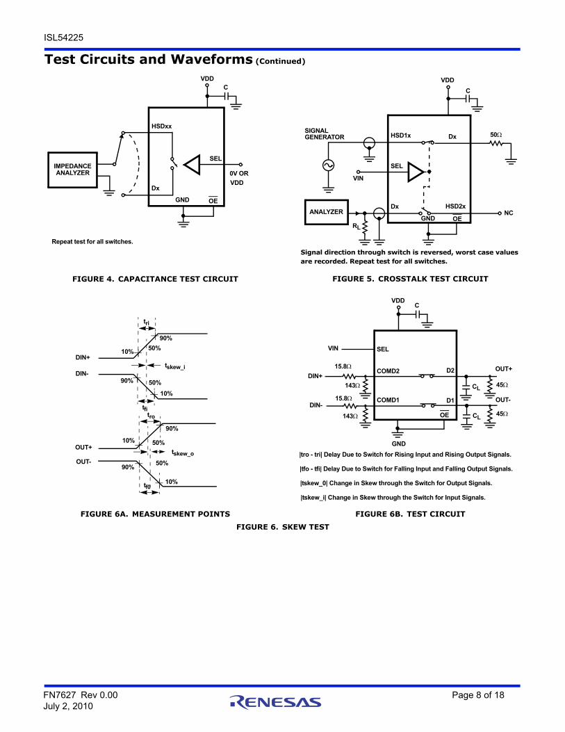
ISL54225
FIGURE 4. CAPACITANCE TEST CIRCUIT FIGURE 5. CROSSTALK TEST CIRCUIT
FIGURE 6A. MEASUREMENT POINTS FIGURE 6B. TEST CIRCUIT
FIGURE 6. SKEW TEST
Test Circuits and Waveforms (Continued)
VDDC
GND
HSDxx
Dx
SELIMPEDANCEANALYZER 0V OR
Repeat test for all switches.
OE
VDD
ANALYZER
VDD
C
HSD1xSIGNALGENERATOR
RL
GND
SEL
Dx 50
NCDx HSD2x
Signal direction through switch is reversed, worst case valuesare recorded. Repeat test for all switches.
OE
VIN
DIN+
DIN-
OUT+
OUT-
50%
50%
90%
10%
10%
10%
10%
90%
90%
50%90%
50%
tri
tfitro
tf0
tskew_i
tskew_o
OUT+
CL
COMD1
D2
GND
VDDC
D1
COMD2
CL
OUT-
DIN+
DIN-
|tro - tri| Delay Due to Switch for Rising Input and Rising Output Signals.
|tfo - tfi| Delay Due to Switch for Falling Input and Falling Output Signals.
|tskew_0| Change in Skew through the Switch for Output Signals.
|tskew_i| Change in Skew through the Switch for Input Signals.
15.8
15.8
143
143
45
45
SELVIN
OE
FN7627 Rev 0.00 Page 8 of 18July 2, 2010
ISL54225
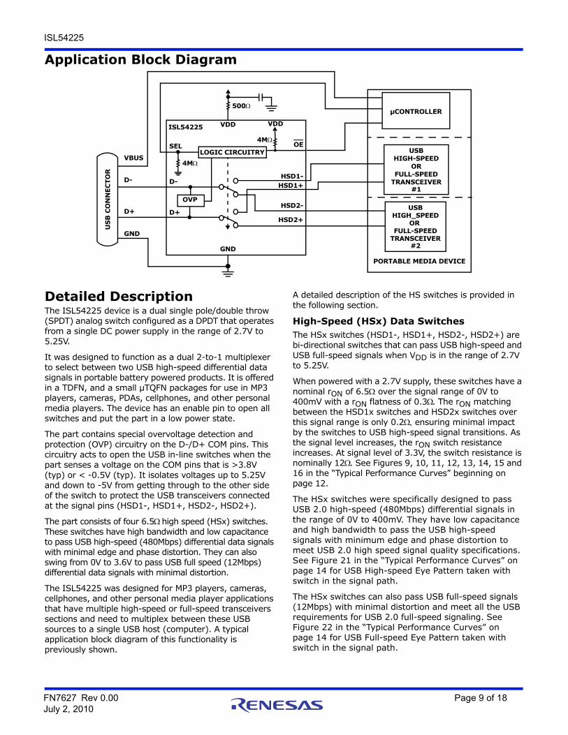
Application Block Diagram
Detailed DescriptionThe ISL54225 device is a dual single pole/double throw (SPDT) analog switch configured as a DPDT that operates from a single DC power supply in the range of 2.7V to 5.25V.
It was designed to function as a dual 2-to-1 multiplexer to select between two USB high-speed differential data signals in portable battery powered products. It is offered in a TDFN, and a small µTQFN packages for use in MP3 players, cameras, PDAs, cellphones, and other personal media players. The device has an enable pin to open all switches and put the part in a low power state.
The part contains special overvoltage detection and protection (OVP) circuitry on the D-/D+ COM pins. This circuitry acts to open the USB in-line switches when the part senses a voltage on the COM pins that is >3.8V (typ) or < -0.5V (typ). It isolates voltages up to 5.25V and down to -5V from getting through to the other side of the switch to protect the USB transceivers connected at the signal pins (HSD1-, HSD1+, HSD2-, HSD2+).
The part consists of four 6.5high speed (HSx) switches. These switches have high bandwidth and low capacitance to pass USB high-speed (480Mbps) differential data signals with minimal edge and phase distortion. They can also swing from 0V to 3.6V to pass USB full speed (12Mbps) differential data signals with minimal distortion.
The ISL54225 was designed for MP3 players, cameras, cellphones, and other personal media player applications that have multiple high-speed or full-speed transceivers sections and need to multiplex between these USB sources to a single USB host (computer). A typical application block diagram of this functionality is previously shown.
A detailed description of the HS switches is provided in the following section.
High-Speed (HSx) Data Switches The HSx switches (HSD1-, HSD1+, HSD2-, HSD2+) are bi-directional switches that can pass USB high-speed and USB full-speed signals when VDD is in the range of 2.7V to 5.25V.
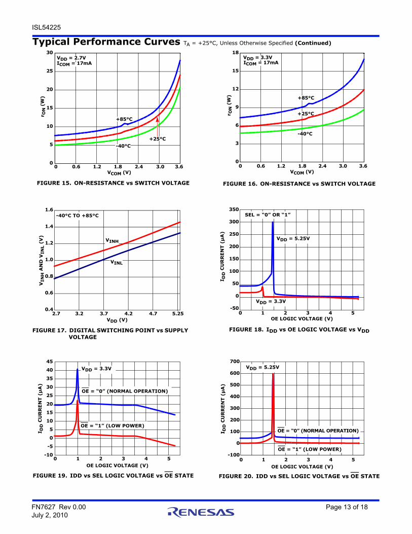
When powered with a 2.7V supply, these switches have a nominal rON of 6.5 over the signal range of 0V to 400mV with a rON flatness of 0.3. The rON matching between the HSD1x switches and HSD2x switches over this signal range is only 0.2 ensuring minimal impact by the switches to USB high-speed signal transitions. As the signal level increases, the rON switch resistance increases. At signal level of 3.3V, the switch resistance is nominally 12. See Figures 9, 10, 11, 12, 13, 14, 15 and 16 in the “Typical Performance Curves” beginning on page 12.
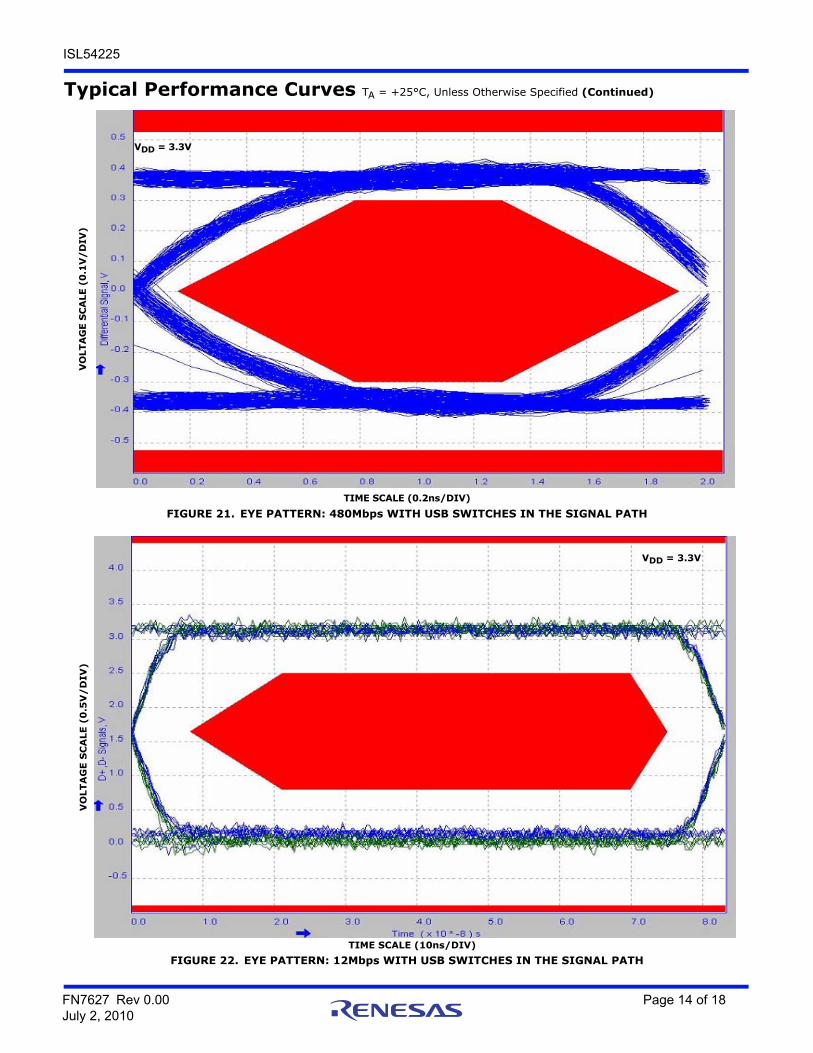
The HSx switches were specifically designed to pass USB 2.0 high-speed (480Mbps) differential signals in the range of 0V to 400mV. They have low capacitance and high bandwidth to pass the USB high-speed signals with minimum edge and phase distortion to meet USB 2.0 high speed signal quality specifications. See Figure 21 in the “Typical Performance Curves” on page 14 for USB High-speed Eye Pattern taken with switch in the signal path.
The HSx switches can also pass USB full-speed signals (12Mbps) with minimal distortion and meet all the USB requirements for USB 2.0 full-speed signaling. See Figure 22 in the “Typical Performance Curves” on page 14 for USB Full-speed Eye Pattern taken with switch in the signal path.
PORTABLE MEDIA DEVICE
ISL54225
USB
TRANSCEIVER
HIGH-SPEED
US
B C
ON
NEC
TOR
D-
D+
SEL
GND
HSD1-HSD1+
HSD2-
HSD2+
VDD
OELOGIC CIRCUITRY
µCONTROLLER
USB
TRANSCEIVERFULL-SPEED
VBUS
D-
D+
GND
ORFULL-SPEED
HIGH_SPEEDOR
OVP#1
#2
4M
4M
500
VDD
FN7627 Rev 0.00 Page 9 of 18July 2, 2010

ISL54225
The HS1 channel switches are active (turned ON) whenever the SEL voltage is logic “0”(Low) and the OE voltage is logic “0”(Low).
The HS2 channel switches are active (turned ON) whenever the SEL voltage is logic “1” (High) and the OE voltage is logic “0” (Low).
OVERVOLTAGE PROTECTION (OVP)The maximum normal operating signal range for the HSx switches is from 0V to 3.6V. For normal operation, the signal voltage should not be allowed to exceed these voltage levels or go below ground by more than -0.3V.
However, in the event that a positive voltage > 3.8V (typ) to 5.25V, such as the USB 5V VBUS voltage, gets shorted to one or both of the COM+ and COM- pins or a negative voltage < -0.5V (typ) to -5V gets shorted to one or both of the COM pins, the ISL54225 has OVP circuitry to detect the overvoltage condition and open the SPDT switches to prevent damage to the USB down-stream transceivers connected at the signal pins (HS1D-, HS1D+, HS2D-, HS2D+).
The OVP and power-off protection circuitry allows the COM pins (D-, D+) to be driven up to 5.25V while the VDD supply voltage is in the range of 0V to 5.25V. In this condition, the part draws < 100µA of ICOMx and IDD current and causes no stress to the IC. In addition, the SPDT switches are OFF and the fault voltage is isolated from the other side of the switch.
External VDD Series Resistor to Limit IDD Current during Negative OVP ConditionA 100Ω to 1kΩ resistor in series with the VDD pin (see Figure 7) is required to limit the IDD current draw from the system power supply rail during a negative OVP fault event.
With a negative -5V fault voltage at both COM pins, the graph in Figure 8 shows the IDD current draw for different external resistor values for supply voltages of 2.7V, 3.6V, and 5.25V. With a 500Ω resistor, the current draw is limited to around 5mA. When the negative fault voltage is removed, the IDD current will return to it’s normal operation current of 25µA to 45µA.
The series resistor also provides improved ESD and latch-up immunity. During an overvoltage transient event (such as occurs during system level IEC 61000 ESD testing), substrate currents can be generated in the IC that can trigger parasitic SCR structures to turn ON, creating a low impedance path from the VDD power supply to ground. This will result in a significant amount of current flow in the IC, which can potentially create a latch-up state or permanently damage the IC. The external VDD resistor limits the current during this over-stress situation and has been found to prevent latch-up or destructive damage for many overvoltage transient events.
Under normal operation, the low microamp IDD current of the IC produces an insignificant voltage drop across the series resistor resulting in no impact to switch operation or performance.
ISL54225 Operation The following will discuss using the ISL54225 shown in the “Application Block Diagram” on page 9.
POWERThe power supply connected at the VDD pin provides the DC bias voltage required by the ISL54225 part for proper operation. The ISL54225 can be operated with a VDD voltage in the range of 2.7V to 5.25V.
For lowest power consumption you should use the lowest VDD supply.
A 0.01µF or 0.1µF decoupling capacitor should be connected from the VDD pin to ground to filter out any power supply noise from entering the part. The capacitor should be located as close to the VDD pin as possible.
In a typical application, VDD will be in the range of 2.8V to 4.3V and will be connected to the battery or LDO of the portable media device.
FIGURE 7. VDD SERIES RESISTOR TO LIMIT IDD CURRENT DURING NEGATIVE OVP AND FOR ENHANCED ESD AND LATCH-UP IMMUNITY
FIGURE 8. NEGATIVE OVP IDD CURRENT vs RESISTOR VALUE vs VSUPPLY
SEL
D+
D-
GND
OVP
LOGIC
VDD
OE
HSD1+
100Ω to 1kΩ
VSUPPLYC
PROTECTIONRESISTOR
HSD1-
IDD
-5VFAULTVOLTAGE
HSD2+
HSD2-
0
5
10
15
20
25
100 200 300 400 500 600 700 800 900 1kRESISTOR (Ω)
I DD
(m
A)
VCOM+ = VCOM- = -5V
2.7V
3.6V
5.25V
FN7627 Rev 0.00 Page 10 of 18July 2, 2010
ISL54225
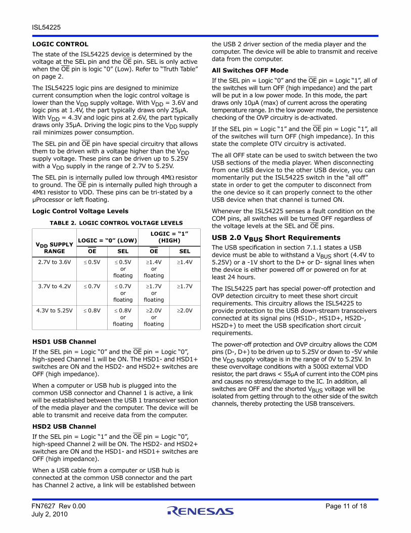
LOGIC CONTROLThe state of the ISL54225 device is determined by the voltage at the SEL pin and the OE pin. SEL is only active when the OE pin is logic “0” (Low). Refer to “Truth Table” on page 2.
The ISL54225 logic pins are designed to minimize current consumption when the logic control voltage is lower than the VDD supply voltage. With VDD = 3.6V and logic pins at 1.4V, the part typically draws only 25µA. With VDD = 4.3V and logic pins at 2.6V, the part typically draws only 35µA. Driving the logic pins to the VDD supply rail minimizes power consumption.
The SEL pin and OE pin have special circuitry that allows them to be driven with a voltage higher than the VDD supply voltage. These pins can be driven up to 5.25V with a VDD supply in the range of 2.7V to 5.25V.
The SEL pin is internally pulled low through 4Mresistor to ground. The OE pin is internally pulled high through a 4M resistor to VDD. These pins can be tri-stated by a µProcessor or left floating.
Logic Control Voltage Levels
HSD1 USB ChannelIf the SEL pin = Logic “0” and the OE pin = Logic “0”, high-speed Channel 1 will be ON. The HSD1- and HSD1+ switches are ON and the HSD2- and HSD2+ switches are OFF (high impedance).
When a computer or USB hub is plugged into the common USB connector and Channel 1 is active, a link will be established between the USB 1 transceiver section of the media player and the computer. The device will be able to transmit and receive data from the computer.
HSD2 USB ChannelIf the SEL pin = Logic “1” and the OE pin = Logic “0”, high-speed Channel 2 will be ON. The HSD2- and HSD2+ switches are ON and the HSD1- and HSD1+ switches are OFF (high impedance).
When a USB cable from a computer or USB hub is connected at the common USB connector and the part has Channel 2 active, a link will be established between
the USB 2 driver section of the media player and the computer. The device will be able to transmit and receive data from the computer.
All Switches OFF ModeIf the SEL pin = Logic “0” and the OE pin = Logic “1”, all of the switches will turn OFF (high impedance) and the part will be put in a low power mode. In this mode, the part draws only 10µA (max) of current across the operating temperature range. In the low power mode, the persistence checking of the OVP circuitry is de-activated.
If the SEL pin = Logic “1” and the OE pin = Logic “1”, all of the switches will turn OFF (high impedance). In this state the complete OTV circuitry is activated.
The all OFF state can be used to switch between the two USB sections of the media player. When disconnecting from one USB device to the other USB device, you can momentarily put the ISL54225 switch in the “all off” state in order to get the computer to disconnect from the one device so it can properly connect to the other USB device when that channel is turned ON.
Whenever the ISL54225 senses a fault condition on the COM pins, all switches will be turned OFF regardless of the voltage levels at the SEL and OE pins.
USB 2.0 VBUS Short RequirementsThe USB specification in section 7.1.1 states a USB device must be able to withstand a VBUS short (4.4V to 5.25V) or a -1V short to the D+ or D- signal lines when the device is either powered off or powered on for at least 24 hours.
The ISL54225 part has special power-off protection and OVP detection circuitry to meet these short circuit requirements. This circuitry allows the ISL54225 to provide protection to the USB down-stream transceivers connected at its signal pins (HS1D-, HS1D+, HS2D-, HS2D+) to meet the USB specification short circuit requirements.
The power-off protection and OVP circuitry allows the COM pins (D-, D+) to be driven up to 5.25V or down to -5V while the VDD supply voltage is in the range of 0V to 5.25V. In these overvoltage conditions with a 500Ω external VDD resistor, the part draws < 55µA of current into the COM pins and causes no stress/damage to the IC. In addition, all switches are OFF and the shorted VBUS voltage will be isolated from getting through to the other side of the switch channels, thereby protecting the USB transceivers.
TABLE 2. LOGIC CONTROL VOLTAGE LEVELS
VDD SUPPLY RANGE
LOGIC = “0” (LOW)LOGIC = “1”
(HIGH)
OE SEL OE SEL
2.7V to 3.6V 0.5V 0.5V or
floating
1.4Vor
floating
1.4V
3.7V to 4.2V 0.7V 0.7V or
floating
1.7Vor
floating
1.7V
4.3V to 5.25V 0.8V 0.8V or
floating
2.0Vor
floating
2.0V
FN7627 Rev 0.00 Page 11 of 18July 2, 2010

ISL54225
Typical Performance Curves TA = +25°C, Unless Otherwise Specified
FIGURE 9. ON-RESISTANCE vs SUPPLY VOLTAGE vs SWITCH VOLTAGE
FIGURE 10. ON-RESISTANCE vs SUPPLY VOLTAGE vs SWITCH VOLTAGE
FIGURE 11. ON-RESISTANCE vs SUPPLY VOLTAGE vs SWITCH VOLTAGE
FIGURE 12. ON-RESISTANCE vs SWITCH VOLTAGE
FIGURE 13. ON-RESISTANCE vs SWITCH VOLTAGE FIGURE 14. ON-RESISTANCE vs SWITCH VOLTAGE
5.6
5.7
5.8
5.9
6.0
6.1
6.2
6.3
6.4
6.5
0 0.1 0.2 0.3 0.4
r ON
(
)
VCOM (V)
ICOM = 17mA
2.7V
3.0V
3.3V
3.6V4.3V
5.25V
3.0V
0
5
10
15
20
25
30
0 0.6 1.2 1.8 2.4 3.0 3.6
r ON
(
)
VCOM (V)
3.3V
ICOM = 17mA
2.7V
4
6
8
10
12
0 0.6 1.2 1.8 2.4 3.0 3.6
r ON
(
)
VCOM (V)
ICOM = 17mA
3.6V
5.25V 4.3V
4
5
6
7
8
0 0.1 0.2 0.3 0.4
r ON
(
)
VCOM (V)
+25°C
+85°C
-40°C
ICOM = 17mA
VDD = 2.7V
4
5
6
7
8
0 0.1 0.2 0.3 0.4
r ON
(
)
VCOM (V)
+25°C
+85°C
-40°C
ICOM = 17mA
VDD = 3.3V
4
5
6
7
8
0 0.1 0.2 0.3 0.4
r ON
(
)
VCOM (V)
+25°C
+85°C
-40°C
ICOM = 17mAVDD = 4.3V
FN7627 Rev 0.00 Page 12 of 18July 2, 2010
ISL54225
FIGURE 15. ON-RESISTANCE vs SWITCH VOLTAGE FIGURE 16. ON-RESISTANCE vs SWITCH VOLTAGE
FIGURE 17. DIGITAL SWITCHING POINT vs SUPPLY VOLTAGE
FIGURE 18. IDD vs OE LOGIC VOLTAGE vs VDD
FIGURE 19. IDD vs SEL LOGIC VOLTAGE vs OE STATE FIGURE 20. IDD vs SEL LOGIC VOLTAGE vs OE STATE
Typical Performance Curves TA = +25°C, Unless Otherwise Specified (Continued)
0
5
10
15
20
25
30
0 0.6 1.2 1.8 2.4 3.0 3.6
r ON
(W
)
VCOM (V)
ICOM = 17mA
+85°C
-40°C
VDD = 2.7V
+25°C
0
3
6
9
12
15
18
0 0.6 1.2 1.8 2.4 3.0 3.6
r ON
(W
)
VCOM (V)
+25°C
+85°C
-40°C
ICOM = 17mAVDD = 3.3V
0.4
0.6
0.8
1.0
1.2
1.4
1.6
2.7 3.2 3.7 4.2 4.7 5.25VDD (V)
VIN
H A
ND
VIN
L (V
)
VINH
VINL
-40°C TO +85°C
-50
0
50
100
150
200
250
300
350
0 1 2 3 4 5OE LOGIC VOLTAGE (V)
I DD
CU
RR
ENT
(µA
)
VDD = 5.25V
VDD = 3.3V
SEL = “0” OR “1”
-10
-5
0
5
10
15
20
25
30
35
40
45
0 1 2 3 4 5
OE = “0” (NORMAL OPERATION)
OE = “1” (LOW POWER)
VDD = 3.3V
OE LOGIC VOLTAGE (V)
I DD
CU
RR
ENT
(µ
A)
-100
0
100
200
300
400
500
600
700
0 1 2 3 4 5OE LOGIC VOLTAGE (V)
I DD
CU
RR
ENT
(µ
A)
OE = “0” (NORMAL OPERATION)
OE = “1” (LOW POWER)
VDD = 5.25V
FN7627 Rev 0.00 Page 13 of 18July 2, 2010
ISL54225
FIGURE 21. EYE PATTERN: 480Mbps WITH USB SWITCHES IN THE SIGNAL PATH
FIGURE 22. EYE PATTERN: 12Mbps WITH USB SWITCHES IN THE SIGNAL PATH
Typical Performance Curves TA = +25°C, Unless Otherwise Specified (Continued)V
OLT
AG
E S
CA
LE (
0.1
V/D
IV)
VDD = 3.3V
TIME SCALE (0.2ns/DIV)
TIME SCALE (10ns/DIV)
VO
LTA
GE
SC
ALE
(0
.5V
/D
IV)
VDD = 3.3V
FN7627 Rev 0.00 Page 14 of 18July 2, 2010
ISL54225
FIGURE 23. FREQUENCY RESPONSE FIGURE 24. OFF-ISOLATION
FIGURE 25. CROSSTALK
Die CharacteristicsSUBSTRATE AND TDFN THERMAL PAD POTENTIAL (POWERED UP):
GND
TRANSISTOR COUNT:1297
PROCESS: Submicron CMOS
Typical Performance Curves TA = +25°C, Unless Otherwise Specified (Continued)
-4
-3
-2
-1
0
1
FREQUENCY (Hz)
NO
RM
ALI
ZED
GA
IN (
dB)
1M 10M 100M 1G
VIN = 0dBm, 0.86VDC BIASRL = 50Ω
-110
-100
-90
-80
-70
-60
-50
-40
-30
-20
-10
0.001 0.01 0.1 1 10 100 500FREQUENCY (MHz)
NO
RM
ALI
ZED
GA
IN (
dB)
VIN = 0dBm, 0.2VDC BIASRL = 50Ω
-110
-100
-90
-80
-70
-60
-50
-40
-30
-20
-10
FREQUENCY (MHz)
NO
RM
ALI
ZED
GA
IN (
dB)
VIN = 0dBm, 0.2VDC BIASRL = 50Ω
0.001 0.01 0.1 1 10 100 500
FN7627 Rev 0.00 Page 15 of 18July 2, 2010
ISL54225
Intersil products are manufactured, assembled and tested utilizing ISO9001 quality systems as notedin the quality certifications found at www.intersil.com/en/support/qualandreliability.html
Intersil products are sold by description only. Intersil may modify the circuit design and/or specifications of products at any time without notice, provided that such modification does not, in Intersil's sole judgment, affect the form, fit or function of the product. Accordingly, the reader is cautioned to verify that datasheets are current before placing orders. Information furnished by Intersil is believed to be accurate and reliable. However, no responsibility is assumed by Intersil or its subsidiaries for its use; nor for any infringements of patents or other rights of third parties which may result from its use. No license is granted by implication or otherwise under any patent or patent rights of Intersil or its subsidiaries.
For information regarding Intersil Corporation and its products, see www.intersil.com
For additional products, see www.intersil.com/en/products.html
© Copyright Intersil Americas LLC 2010. All Rights Reserved.All trademarks and registered trademarks are the property of their respective owners.
ProductsIntersil Corporation is a leader in the design and manufacture of high-performance analog semiconductors. The Company's products address some of the industry's fastest growing markets, such as, flat panel displays, cell phones, handheld products, and notebooks. Intersil's product families address power management and analog signal processing functions. Go to www.intersil.com/products for a complete list of Intersil product families.
*For a complete listing of Applications, Related Documentation and Related Parts, please see the respective device information page on intersil.com: ISL54225
To report errors or suggestions for this datasheet, please go to www.intersil.com/askourstaff
FITs are available from our website at http://rel.intersil.com/reports/search.php
Revision HistoryThe revision history provided is for informational purposes only and is believed to be accurate, but not warranted. Please go to web to make sure you have the latest Rev.
DATE REVISION CHANGE
7/2/10 FN7627.0 Initial Release.
FN7627 Rev 0.00 Page 16 of 18July 2, 2010

ISL54225
FN7627 Rev 0.00 Page 17 of 18July 2, 2010
Package Outline Drawing
L10.1.8x1.4A10 LEAD ULTRA THIN QUAD FLAT NO-LEAD PLASTIC PACKAGERev 5, 3/10
located within the zone indicated. The pin #1 identifier may be
Unless otherwise specified, tolerance : Decimal ± 0.05
JEDEC reference MO-255.
The configuration of the pin #1 identifier is optional, but must be
between 0.15mm and 0.30mm from the terminal tip.
Dimension applies to the metallized terminal and is measured
Dimensions in ( ) for Reference Only.
Dimensioning and tolerancing conform to ASME Y14.5m-1994.
6.
either a mold or mark feature.
3.
5.
4.
2.
Dimensions are in millimeters.1.
NOTES:
BOTTOM VIEW
DETAIL "X"
SIDE VIEW
TYPICAL RECOMMENDED LAND PATTERN
TOP VIEW
0.08SEATING PLANE
0.10 C
C
C
SEE DETAIL "X"
MAX. 0.55
0 .1 27 REF
0-0.05
C
2X
0.10
1.4
0
1.80
B
A
67
1
5
6X 0.40
CC
4
0.10MM A B
0.70
PIN #1 ID
2
10
INDEX AREAPIN 1
0.50
10X 0.20
6
6
4X 0.30
0.05
1
3
8
9 X 0.40
6 7
1
5
(6X 0.40)
(0.70)
10 (0.70)(10X 0.20)
(4X 0.30)
3
8
(9 X 0.60)
PACKAGE OUTLINE
ISL54225
FN7627 Rev 0.00 Page 18 of 18July 2, 2010
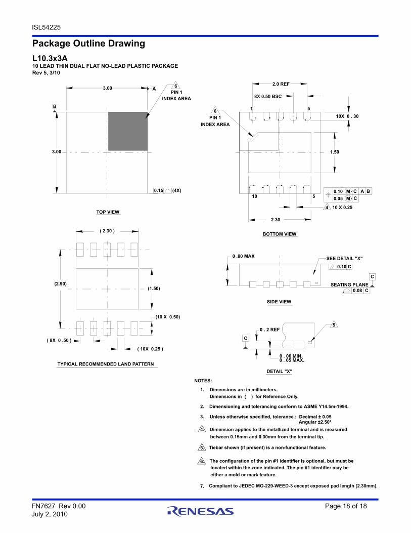
Package Outline Drawing
L10.3x3A10 LEAD THIN DUAL FLAT NO-LEAD PLASTIC PACKAGERev 5, 3/10
located within the zone indicated. The pin #1 identifier may be
Unless otherwise specified, tolerance : Decimal ± 0.05
Tiebar shown (if present) is a non-functional feature.
The configuration of the pin #1 identifier is optional, but must be
between 0.15mm and 0.30mm from the terminal tip.
Dimension applies to the metallized terminal and is measured
Dimensions in ( ) for Reference Only.
Dimensioning and tolerancing conform to ASME Y14.5m-1994.
6.
either a mold or mark feature.
3.
5.
4.
2.
Dimensions are in millimeters.1.
NOTES:
BOTTOM VIEW
DETAIL "X"
SIDE VIEW
TYPICAL RECOMMENDED LAND PATTERN
TOP VIEW
INDEX AREA
(10 X 0.50)
(2.90)
( 8X 0 .50 )
( 10X 0.25 )
(1.50)
0 . 05 MAX.0 . 00 MIN.
0 . 2 REF5
(4X)
( 2.30 )
3.00
0.15
0 .80 MAX
2.30
10
SEE DETAIL "X"
0.10 C
5
1.50
INDEX AREA
B
3.00 A
PIN 16
PIN 16
1
2.0 REF
8X 0.50 BSC
5
C
SEATING PLANEC0.08
BC0.10 M A
10 X 0.254
M0.05 C
10X 0 . 30
C
Angular ±2.50°
Compliant to JEDEC MO-229-WEED-3 except exposed pad length (2.30mm).7.
Related Documents


