IS2.3-6 Wide Bandgap (WBG) Power Devices for High-Density Power Converters – Excitement and Reality Krishna Shenai, Ph.D. Principal Electrical Engineer, Argonne National Laboratory Senior Fellow, NAISE, Northwestern University Senior Fellow, Computation Institute, University of Chicago APEC 2014, Fort Worth, TX Industry Session Paper – IS2.3-6 Wednesday , March19, 2014 2:00 pm – 5:30 pm

Welcome message from author
This document is posted to help you gain knowledge. Please leave a comment to let me know what you think about it! Share it to your friends and learn new things together.
Transcript

IS2.3-6 Wide Bandgap (WBG) Power Devices
for High-Density Power Converters
– Excitement and Reality
Krishna Shenai, Ph.D. Principal Electrical Engineer, Argonne National Laboratory Senior Fellow, NAISE, Northwestern University
Senior Fellow, Computation Institute, University of Chicago APEC 2014, Fort Worth, TX Industry Session Paper – IS2.3-6 Wednesday , March19, 2014 2:00 pm – 5:30 pm

Implications of WBG Materials on Transportation Power Electronics
Compact energy-efficient power train and EV charging systems
2
Current state of a traction drive rated at 55 kW peak for 18 sec., 30 kW continuous and 15 years lifetime
An example of traction inverter cost breakdown
Source: DOE VTO
G. Cameron et al, Proc. EVS26, 2012

Design for Reliability
Power Electronics Systems
Should be Built-to-Last Under
Appropriate Field-Operating
Conditions.
WBG data sheet statement:
“This product has not been designed or tested for use in, and is not intended for use
in, applications implanted into the human body nor in applications in which the failure
of the product could lead to death, personal injury or property damage, including but
not limited to equipment used in the operation of nuclear facilities, life-support
machines, cardiac defibrillators or similar emergency equipment, aircraft navigation or
communication or control systems, air traffic control systems, or weapons systems.”
3

What does this mean?
High-end computer server power supplies
demand an MTBF ~ 1,000,000 hours
4
10 kW Delta Supply

How are today’s power converters designed?
Automotive traction inverters and battery chargers
demand MTBF > 500,000 hours 5

Power Semiconductor Switching Stresses
6

Power Semiconductor Switch Module
Tc
Ts
Ta
Chip
Interface
Heatsink
Conduction
Convection
Zjc
Zcs
Zsa
Ploss
(a) (b)
Tjmax
7

“Industry-Best” SiC Power MOSFETs
1,200V Cree MOSFET
Rsp = 3.7 mΩ.cm2 1,200V Rohm MOSFET
Rsp = 2.6 mΩ.cm2
8

“Industry-Best” GaN Power Switches
600V Panasonic GIT
Rsp = 2.5 mΩ.cm2
9

WBG Power Technology Roadmap
10 250 400 600 900 1,200 1,700
BLOCKING VOLTAGE (VOLTS)
RE
PE
TIT
IVE
SW
ITC
HIN
G C
UR
RE
NT
(A
MP
S)
10
50
100
300
500
Vertical SiC Switch
Automotive Lighting
Computing Motor Control
Power Grid Integration
SiC
Lateral GaN Switch
GaN/Si
PoL DC-DC Converter Automotive
Lighting Computing
Communication
Current commercial applications Emerging high-
voltage and High-power applications
Vertical devices
SiC and GaN power devices will make converters more compact and energy-efficient, and will enable new applications
Ne
ed
low
-co
st r
elia
ble
WB
G p
ow
er
swit
ch
10
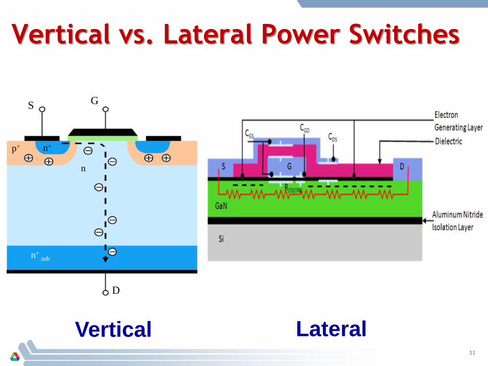
Vertical vs. Lateral Power Switches
S G
D
n
n+ sub
n+ p+
Vertical Lateral 11

Unipolar Power Switch
Vertical Lateral
12

“Industry Standard”
𝑅𝑠𝑝 = 4𝑉𝐵
2
𝜀𝑠µ𝐸𝑐3 (1𝑎)
𝑄𝑔 = 𝐶𝑖𝑠𝑠 𝑉𝑔𝑠 (1𝑏)
𝑅𝑠𝑝𝑙 = 𝑉𝐵
2
𝑞𝜇𝑠𝑛𝑠𝐸𝑐2 (3)
K. Shenai et al, IEEE Electron Device Letters, vol. 35, no. 12, p. 2459, Dec. 1988
13

Specific On-State Resistance
K. Shenai et al, IEEE Trans. Electron Devices, vol. 36, no. 9, pp. 1811-1823, Sep. 1989
14

Thermal Failures in Electronics
Avionics Integrity Program (AVIP), MIL-STD-1796A (USAF), October 13, 2011
15

Localized Failure in Power Semiconductors
16 M. Trivedi and K. Shenai, IEEE Trans. PELS, vol. 14, no. 1, pp. 108-116, Jan. 1999

Thermal “Figure of Merit”
100
101
102
103
104
105
106
101 102 103 104
Breakdown Voltage (V)
GaN Lateral
SiC Vertical
GaN Vertical
QF2
/ Q
F2 (
Si)
𝑄𝐹2 = 𝜅𝜎𝑠𝑝𝐸𝑐
K. Shenai et al, ECS J. Solid State Sci. & Technol., vol. 2, no. 8, pp. N3055-N3063, Jul. 2013 17

Why WBG Power
Semiconductors are not in the
Transportation Sector?
- Reality !
18

On-State Resistance
19
Typical Output Characteristic (Tj = 25°C) Typical Output Characteristic (Tj = 150°C)
On Resistance vs. Temperature (VGS = 20 V)
On-resistance data is inconsistent with I-V data

Body Diode Characteristics
20 20
Typical Body Diode Characteristic (Tj = 25°C) Typical Body Diode Characteristic (Tj = 25°C)
Strong indication of the
Influence of gate oxide charge

Measured dv/dt of SiC Power Diodes
dv/dt (V/nsec.)
Tc = 25°C
0
1.5
3
4.5
6
0 15 30 45 60
SW2
PD2
Pea
k D
iod
e C
urr
ent
(A)
Failure Instant
SW2: 600V/6A 4H-SiC JBS diode
PD2: 600V/8A silicon MPS diode
SD1: 300V/10A 4H-SiC JBS diode
SW1: 200V/12A silicon MPS diode
WBG data sheets do not provide dv/dt ratings
K. Acharya and K. Shenai, Power Electronics Technology, pp. 672-677, Oct. 2002
21

Manufacturer Report on dv/dt
22
Turn-on dv/dt = 75 V/ns
Turn-off dv/dt = 100 V/ns
Cree Report # CPWR-RS01, Rev A
Does not make any sense!

Measured Avalanche Energy of Diodes
600V/8A 4H-SiC JBS diode 600V/6A silicon MPS diode
WBG data sheets do not provide avalanche energy ratings
K. Shenai et al, Proc. IEEE, Jan. 2014
23

24
Safe Operating Area (SOA)
Why SiC SOA is
smaller than
silicon?

Silicon Carbide MOSFET Gate Oxide Failures
25

4H-SiC Material Defects and MOS Gate Oxide Reliability
SiC MOS gate oxide charge and poor reliability originate from material defects in the epitaxial region
26
K. Yamamoto et al, Mat. Sci. Forum, vols. 717-720 (2012), pp. 477-480.

Substrate Effect on Heat Removal
Package Layout Thermal Model
27

Preliminary Results
K. Shenai, to appear in Proc. GOMACTECH Conference, Mar. 2014 28
(a)
(b)
(c)
(a) Thermal impedance and (b) Tjmax vs. substrate thickness for 600V/24A silicon SJT, and (c) estimated Tjmax for 1,200V power transistors fabricated on various substrate materials when dissipating 10W power in the on-state.

Where do we go from here?
- Need a New Approach !
29

Present PVT SiC Crystal Growth Process
SiC seed
Vertical (c-axis) 4H-SiC boule growth
proceeds from top surface of large-area
seed via hundreds to thousands of
threading screw dislocations (TSDs).
Crystal grown at T > 2200 °C --> High thermal gradient & stress --> More dislocations
Growth in the c-axis direction, enabled by screw-dislocations providing steps!
After Ohtani et al. J. Cryst. Growth 210 p. 613.
Threading screw dislocation growth spirals
(THE sources of steps for c-axis growth)
found at top of grown 4H-SiC boule.
Contention: Elimination of screw dislocations from power devices not possible while
maintaining commercially viable crystal quality and growth rate and via this approach.
c-ax
is
30

Defects in SiC Material
31

Joint OSD/Army/Navy SiC HEPS ManTech
Reduce substrate and drift-region defect density
• Role of TEDs and TSDs not investigated • Radically new bulk and epi crystal growth processes may be
needed in order to further reduce and/or eliminate TEDs and TSDs
• Yield and cost metrics are not well-defined • Not directly applicable to commercial power devices
M. Loboda, DOW CORNING, ICSCRM 2011 Industry Session 100 mm wafers Micropipe Density ~ 0 cm-2 Threading Screw Dislocation Density < 1,000 cm-2 Basal Plane Dislocation Density < 1,000 cm-2
4 in. dia.
6 in. dia.
Key Objectives:
• Increase wafer dia. from 4” to 6” • Increase voltage ratings by 2-3X of Si rating • Bring down die cost to within 2-2.5X of Si cost • Reliable operation up to TC = 150⁰C (vs. 70⁰C for Si)
Si and SiC IGBTs
Parameter Baseline (4” dia. median)
Best R&D in FY13
(6” dia.)
Commercial (6” dia. median)
Micro-pipes (cm-2)
< 0.8 < 0.8 < 0.2
TEDs and TSDs (cm-2)
275 2,000 800
BPDs in epi (cm-2) < 2 (50 μm) < 50 (75 μm) < 1 (160 μm)
Epi thickness/doping uniformity/thickness
2%/5%/75 μm 2%/20%/75 μm
1%/6%/160 μm
32
TED and TSD densities are higher for 6 in. dia. wafers

Key Device Challenge
n-
n+
WD
≈
≈
K
A Anode Contact
Cathode Contact
Epi Defects - Killer Defects
Bulk Defects - Causal Defects
Consequences: • Voltage De-Rating • Limited Die Size • Poor Wafer Yield • High Cost • Less Than Optimal Performance • Field-Reliability Unknown • Bipolar power switch questionable
300 amps Six 50 amp dice
There are other challenges
High starting Wafer Cost Epi Uniformity
Gate Dielectrics Contacts
HV Passivation Carreer Lifetime Control
……. K. Shenai, Interface, Electrochemical Society, vol. 22, no. 1, pp.
47-53, Spring 2013 (invited paper). 33

Material – Device – Module – Converter Interaction
34

Key Material Challenge
VBD (V)
100
2,000 25 50
SiC
100,000
~
~
GaN
SiC
GaN
I ON
(A
)
50 Bulk Material
Defect Density
< 100 cm-2
25
Reliable Switching Current
Density > 200 A/cm2
TJMAX > 200°C
K. Shenai, Interface, Electrochemical Society, vol. 22, no. 1, pp. 47-53, Spring
2013 (invited paper). 35

Summary and Recommendations
• WBG power devices have the potential for transformative advances in transportation sector. • Progress is severely hampered by a high density of crystal defects in WBG semiconductors. • Need reliability-driven application engineering with improved data sheets in order to infuse WBG power electronics into the transportation sector. • This is a challenge especially since the power electronics industry supply chain is highly fragmented.
36
Related Documents