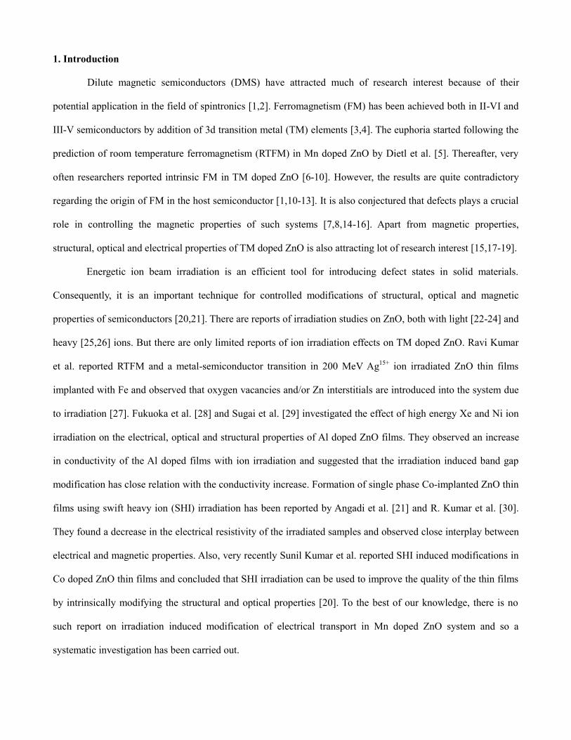
Effect of 50 MeV Li 3+ irradiation on structural and electrical properties of Mn doped ZnO S. K. Neogi 1 , S. Chattopadhyay 2 , Aritra Banerjee 1 , S. Bandyopadhyay 1 , A. Sarkar 3 and Ravi Kumar 4 1 Department of Physics, University of Calcutta, 92 Acharya Prafulla Chandra Road, Kolkata 700009, West Bengal, India 2 Calcutta Institute of Engineering and Management , 24/1A Chandi Ghosh Road, Kolkata 700040, West Bengal, India 3 Department of Physics, Bangabasi Morning College, 19 Rajkumar Chakraborty Sarani, Kolkata 700009, West Bengal, India 4 Department of Material Science & Engineering, NIT, Hamirpur-177005, Himachal Pradesh, India E-mail: [email protected] (Aritra Banerjee) Abstract The present work aims to study the effect of ion irradiation on structural and electrical properties and their correlation with the defects in Zn 1-x Mn x O type system. Zn 1-x Mn x O (x = 0.02, 0.04) samples have been synthesized by solid-state reaction method and have been irradiated with 50 MeV Li 3+ ions. The concomitant changes have been probed by x-ray diffraction (XRD), temperature dependent electrical resistivity and positron annihilation lifetime (PAL) spectroscopy. XRD result shows single phase wurtzite structure for Zn 0.98 Mn 0.02 O, whereas for Zn 0.96 Mn 0.04 O sample an impurity phase has been found apart from the usual peaks of ZnO. Ion irradiation dissolves this impurity peak. Grain size of the samples found to be uniform. For Zn 0.98 Mn 0.02 O, the observed sharp decrease in room temperature resistivity ( RT ) with irradiation is consistent with the lowering of FWHM of the XRD peaks. However for Zn 0.96 Mn 0.04 O, RT decreases for initial fluence but increases for further increase of fluence. All the irradiated Zn 0.98 Mn 0.02 O samples show metal-semiconductor transition in temperature dependent resistivity measurement at low temperature. But all the irradiated Zn 0.96 Mn 0.04 O samples show semiconducting nature in the whole range of temperature. Results of room temperature resistivity, XRD and PAL measurements are consistent with each other. Keywords: Mn doped ZnO; Ion irradiation; Defects; Electrical characterization PACS No:81.05.Dz; 61.80.Jh; 61.72.J-; 61.05.cp; 72.80.-r; 78.70.Bj

Welcome message from author
This document is posted to help you gain knowledge. Please leave a comment to let me know what you think about it! Share it to your friends and learn new things together.
Transcript
Effect of 50 MeV Li3+ irradiation on structural and electrical
properties of Mn doped ZnO
S. K. Neogi1, S. Chattopadhyay
2, Aritra Banerjee
1, S. Bandyopadhyay
1, A. Sarkar
3 and Ravi Kumar
4
1 Department of Physics, University of Calcutta, 92 Acharya Prafulla Chandra Road, Kolkata 700009, West
Bengal, India 2Calcutta Institute of Engineering and Management , 24/1A Chandi Ghosh Road, Kolkata 700040, West Bengal, India
3Department of Physics, Bangabasi Morning College, 19 Rajkumar Chakraborty Sarani, Kolkata 700009, West
Bengal, India 4 Department of Material Science & Engineering, NIT, Hamirpur-177005, Himachal Pradesh, India
E-mail: [email protected] (Aritra Banerjee)
Abstract
The present work aims to study the effect of ion irradiation on structural and electrical properties and
their correlation with the defects in Zn1-xMnxO type system. Zn1-xMnxO (x = 0.02, 0.04) samples have been
synthesized by solid-state reaction method and have been irradiated with 50 MeV Li3+
ions. The concomitant
changes have been probed by x-ray diffraction (XRD), temperature dependent electrical resistivity and positron
annihilation lifetime (PAL) spectroscopy. XRD result shows single phase wurtzite structure for Zn0.98Mn0.02O,
whereas for Zn0.96Mn0.04O sample an impurity phase has been found apart from the usual peaks of ZnO. Ion
irradiation dissolves this impurity peak. Grain size of the samples found to be uniform. For Zn0.98Mn0.02O, the
observed sharp decrease in room temperature resistivity (RT) with irradiation is consistent with the lowering of
FWHM of the XRD peaks. However for Zn0.96Mn0.04O, RT decreases for initial fluence but increases for further
increase of fluence. All the irradiated Zn0.98Mn0.02O samples show metal-semiconductor transition in temperature
dependent resistivity measurement at low temperature. But all the irradiated Zn0.96Mn0.04O samples show
semiconducting nature in the whole range of temperature. Results of room temperature resistivity, XRD and PAL
measurements are consistent with each other.
Keywords: Mn doped ZnO; Ion irradiation; Defects; Electrical characterization
PACS No:81.05.Dz; 61.80.Jh; 61.72.J-; 61.05.cp; 72.80.-r; 78.70.Bj
1. Introduction
Dilute magnetic semiconductors (DMS) have attracted much of research interest because of their
potential application in the field of spintronics [1,2]. Ferromagnetism (FM) has been achieved both in II-VI and
III-V semiconductors by addition of 3d transition metal (TM) elements [3,4]. The euphoria started following the
prediction of room temperature ferromagnetism (RTFM) in Mn doped ZnO by Dietl et al. [5]. Thereafter, very
often researchers reported intrinsic FM in TM doped ZnO [6-10]. However, the results are quite contradictory
regarding the origin of FM in the host semiconductor [1,10-13]. It is also conjectured that defects plays a crucial
role in controlling the magnetic properties of such systems [7,8,14-16]. Apart from magnetic properties,
structural, optical and electrical properties of TM doped ZnO is also attracting lot of research interest [15,17-19].
Energetic ion beam irradiation is an efficient tool for introducing defect states in solid materials.
Consequently, it is an important technique for controlled modifications of structural, optical and magnetic
properties of semiconductors [20,21]. There are reports of irradiation studies on ZnO, both with light [22-24] and
heavy [25,26] ions. But there are only limited reports of ion irradiation effects on TM doped ZnO. Ravi Kumar
et al. reported RTFM and a metal-semiconductor transition in 200 MeV Ag15+
ion irradiated ZnO thin films
implanted with Fe and observed that oxygen vacancies and/or Zn interstitials are introduced into the system due
to irradiation [27]. Fukuoka et al. [28] and Sugai et al. [29] investigated the effect of high energy Xe and Ni ion
irradiation on the electrical, optical and structural properties of Al doped ZnO films. They observed an increase
in conductivity of the Al doped films with ion irradiation and suggested that the irradiation induced band gap
modification has close relation with the conductivity increase. Formation of single phase Co-implanted ZnO thin
films using swift heavy ion (SHI) irradiation has been reported by Angadi et al. [21] and R. Kumar et al. [30].
They found a decrease in the electrical resistivity of the irradiated samples and observed close interplay between
electrical and magnetic properties. Also, very recently Sunil Kumar et al. reported SHI induced modifications in
Co doped ZnO thin films and concluded that SHI irradiation can be used to improve the quality of the thin films
by intrinsically modifying the structural and optical properties [20]. To the best of our knowledge, there is no
such report on irradiation induced modification of electrical transport in Mn doped ZnO system and so a
systematic investigation has been carried out.
2. Experiments
The Zn1-xMnxO (x = 0.02, 0.04) samples were synthesized by conventional solid-state reaction method
[6,16,31]. Stoichiometric amount of ZnO and MnO2 powders (each of purity 99.99%; Sigma-Aldrich, Germany)
have been weighed, mixed and ground together. The samples were initially milled for 32 h followed by
annealing at 400 0
C for 8 h. The resulting powder was again milled for another 64 h. All the milling was
performed in “Fritsch planetary mono mill” machine (Model no: Pulverisette 6) using agate ball and container.
In order to avoid large grain size reduction (and hence to avoid the grain size related effects), the samples have
been milled at ball to mass ratio of 1:1. The powder thus obtained was then pressed into pellets, followed by
final sintering at 500 0C for 12 h. The reasons for choosing 500
0C as the final sintering temperature has been
discussed earlier [31]. The synthesized Zn0.98Mn0.02O and Zn0.96Mn0.04O samples have been irradiated with 50
MeV Li3+
ion beam. The samples have been irradiated at four different fluence of 1 × 10¹²
, 1 × 10¹³
, 5 × 10¹³
and
1 × 10¹⁴
ions/cm2. The irradiation experiment was carried out using a focused beam, carefully scanned over an
area of 1 cm × 1 cm, after mounting the samples on the ladder in high vacuum irradiation chamber. In order to
avoid the possibility of Li implantation related effects, the irradiation experiments were performed on samples of
thickness of around 200 micron, less than the penetration depth (220 micron) of 50 Mev Li3+
ion beam in Mn
doped ZnO.
The phase characterization of the Zn1-xMnxO (x = 0.02, 0.04) samples before and after irradiation has
been carried out using powder x-ray diffractometer [Philips, Model: PW1830] with Cu-K radiation. All X-Ray
Diffraction (XRD) measurements were carried out in the range of 200 < 2 < 80
0 in -2 geometry. The electrical
resistivity as a function of temperature of all the samples was measured using conventional two-probe technique.
A Keithley electrometer (model 6514) was employed to measure the resistance. Positron annihilation lifetime
(PAL) measurement at RT was performed on Zn0.98Mn0.02O sample with 0, 1 × 10¹²
, 5 × 10¹³
ions/cm2 irradiation
fluence. For PAL study, a 10-Ci 22
Na positron source (enclosed in 2 micron thin mylar foil) was sandwiched
between two identical plane faced pellets of the samples. The PAL spectra were measured with a fast-slow
coincidence assembly having 182 + 1 ps time resolution [14]. Measured spectra were analyzed by computer
program PATFIT-88 [32] to obtain the possible lifetime components i and their corresponding intensities Ii.
3. Results and Discussion
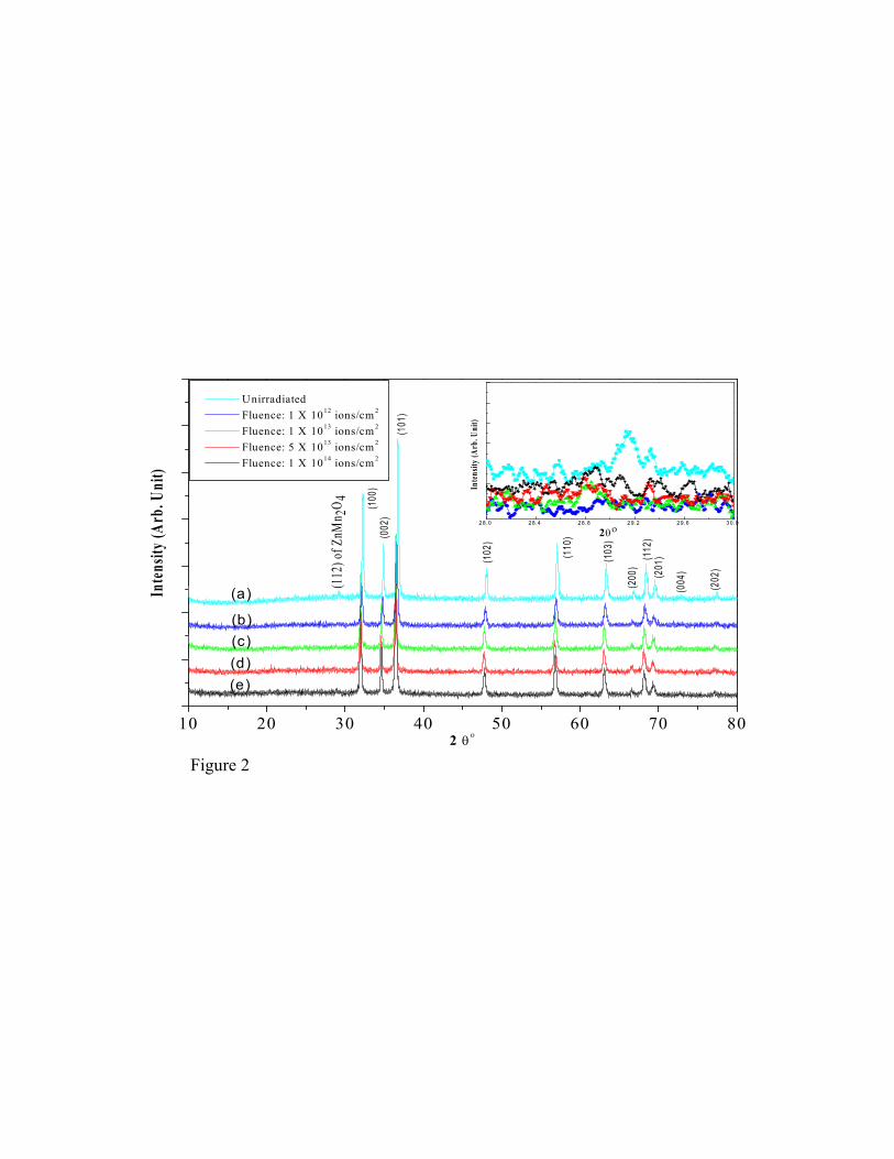
Figure 1 reveals that the synthesized Zn1-xMnxO sample with x=0.02 are in single phase and no traces of
impurity peak has been detected. No detectable amorphisation has been observed up to highest fleunce (1×10¹⁴
ions/cm2) reflecting high radiation hardness of ZnO based systems. For 4 at % Mn doped un-irradiated sample
(figure 2), apart from the peaks corresponding to those of ZnO hexagonal wurtzite structure, a weak (112) peak
of ZnMn2O4 has been observed at 2 = 29.110 [31]. Interestingly, this impurity peak disappeared just after
irradiation with lowest fluence (1×10¹²
ions/cm2), as shown in inset of figure 2. This indicates that the impurity
phase has been dissolved and the sample become single phased, at least within the detection limit of XRD.
Irradiation induced dissolution of impurity phase has also been observed earlier for Ag ion irradiated Co and Fe
doped ZnO thin films [21,27,30]. But for Mn doped ZnO system, probably this is the first report of impurity
phase dissolution using comparatively lighter ion, Li beam irradiation. The irradiated particles after entering the
target suffers a number of collisions both elastic and inelastic and loses its energy via these interactions viz.,
electronic energy loss (Se) and nuclear energy loss (Sn) respectively [20,21,27]. The evaluation using the
simulation program SRIM-2008 [33] showed that the mean electronic energy loss Se and nuclear energy loss Sn
of 50 MeV Li3+
-ions in our synthesized Mn doped ZnO samples are 13.69 eV/Å and 7.65 × 10⁻³
eV/Å,
respectively. Thus irradiated Li ion loses its energy mainly by electronic energy loss process. Transfer of energy
to the lattice, locally, can modify the impurity phase to more stable doped ZnO structure. Thus, in concurrence to
the earlier reports of obtaining single phase TM doped ZnO thin films by ion beam irradiation [20,21,27,30], our
study also lead to possibility of single phase formation in 4 at % Mn doped ZnO with Li ion irradiation.
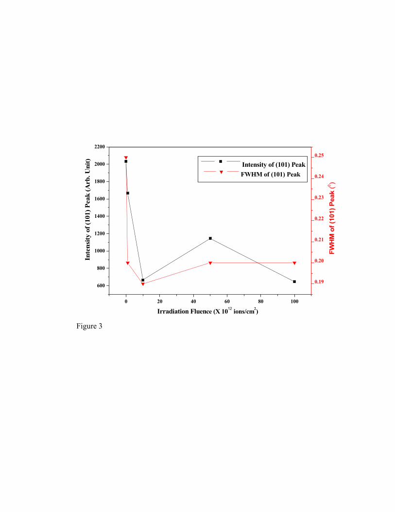
Furthermore, we have monitored the variation of peak intensity as well as FWHM of the most dominant
(101) peak with irradiation fluence. Figure 3 shows that both the intensity and FWHM of the (101) peak of
Zn0.98Mn0.02O, decreases strongly with initial irradiation fluence and gradually saturates at higher fluence. This
decrease in peak intensity along with its decreasing FWHM appears to be contradictory in nature, as far as
crystallinity of the sample is concerned. But this apparent contradicting behavior has also been reported earlier in
100 KeV Ne and 1.2 Mev Ar irradiated ZnO [34,35]. It is noteworthy to mention that, we observed some
peculiar behavior in temperature dependent resistivity data of irradiated Zn0.98Mn0.02O samples, which may have
some correlation with the strange features obtained in XRD for the same samples. In general, polycrystalline
samples are rich in defects. Also the grain boundaries (GB) are much more defective compared to the grain
interiors [36]. During the passage of energetic projectiles the re-organization of defects in the GB region is more
likely due to larger abundance of defects there. Thus, with increasing fluence up to the dose of 1x10¹³
ion/cm2,
the distribution of the grain orientation becomes sharper with increase in grain size, which is reflected in the
decrease in FWHM of the most intense (101) peak [35,37]. Whereas in the grain interiors, before irradiation
which was less defective region, the energy lost by the high energy ion beam also creates some defects. Thus
within each grain, the crystalline quality degrades with increasing ion dose, as also reported by Matsunami et al
[35]. This could explain the decrease of the XRD intensity of the most dominant (101) peak with initial doses of
fluence. Thus high energy ion beam irradiation affect the GB regions and grain interior regions in two mutually
opposite direction, as obtained earlier by Matsunami et al [35]. With further increase of doses of irradiation, the
competition between these two effects leads to homogenization of defects to some extent. Also a saturation of
defects is expected in such case [34, 38]. This is reflected in figure 3, where with irradiation dose the FWHM as
well as peak intensity initially deceases and then gradually saturates for the irradiated Zn0.98Mn0.02O samples.
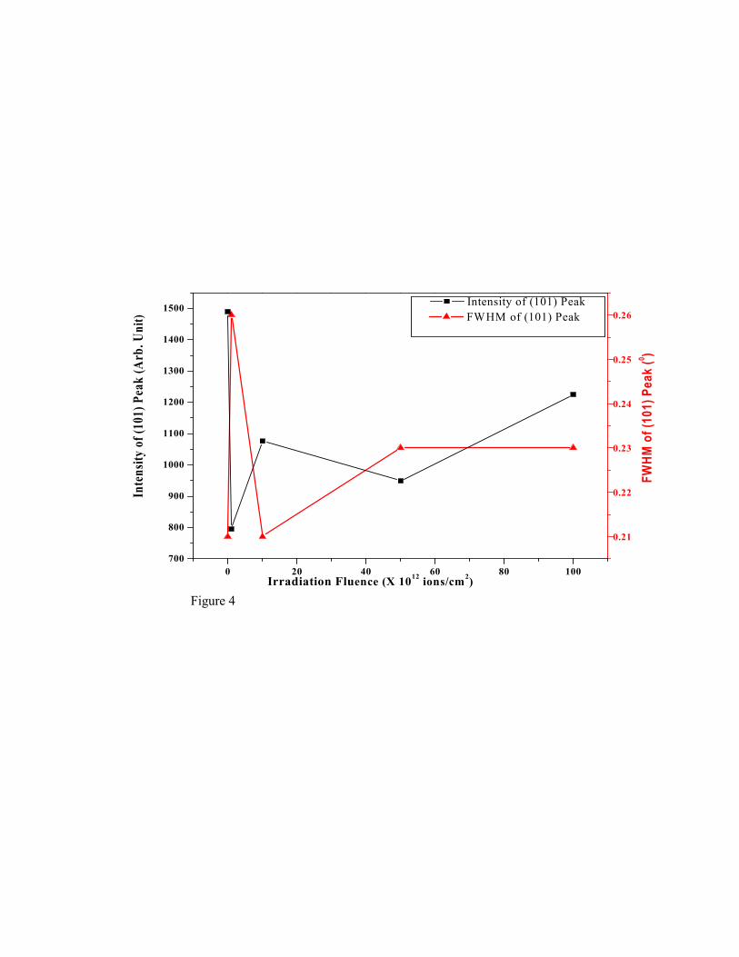
We have also monitored the variation of peak intensity as well as FWHM of the most dominant (101)
XRD peak with irradiation fluence for Zn0.96Mn0.04O (figure 4). For the initial irradiation fluence, unlike
Zn0.98Mn0.02O, FWHM of (101) peak increases and peak intensity decreases for the Zn0.96Mn0.04O sample. It
should be remembered that, the as prepared Zn0.96Mn0.04O sample contains impurity peak of ZnMn2O4 phase,
which dissolve with the lowest dose of fluence. Thus upon irradiated with 1×10¹²
ions/cm2 dose of fluence the
sample becomes single phase in nature. But we found that, with increasing dose of irradiation (1×10¹³
ions/cm2),
the FWHM of the (101) peak decreases and the peak intensity increases and no appreciable change for higher
doses of irradiation (5×10¹³
ions/cm2 to 1×10
14 ions/cm
2). This observation suggests that the crystalline quality
of the 4 at % Mn doped ZnO samples becomes better with higher doses of irradiation. In the present sample the
doping concentration of Mn is higher than Zn0.98Mn0.02O and hence the resultant defective state after irradiation
can be largely different. So, different trend in XRD features is not unexpected.
Close inspection of figure 1 indicates higher angle shift of (101) peak in case of Zn0.98Mn0.02O sample
just after the irradiation with fluence of 1x10¹²
ions/cm2. But with increasing irradiation fluence, there is no
further shift of the (101) peak. This might be due to release of residual strain in the system with irradiation [39].
But in case of Zn0.96Mn0.04O (figure 2) sample XRD peaks shifts towards lower angle after irradiation. It
indicates simply enhancement of lattice parameter. Unirradiated Zn0.96Mn0.04O sample contains impurity peak of
ZnMn2O4, which dissolves just with initial fluence of irradiation (1012
ions/cm2). So incorporation of Mn ions in
host ZnO matrix increases with dissolution of impurity phase. Thus the observed shift of (101) peak towards
lower angle (enhancement of lattice parameter) seems to quiet justified as ionic radii of Mn2+
(0.67 Å) is higher
than that of Zn2+
(0.60 Å) [40]. There must be some higher angle shifting of (101) peak due to release of residual
strain in the system with irradiation in case of Zn0.96Mn0.04O samples also. But lower angle shifting of (101) peak
due to more Mn incorporation with irradiation predominates over the earlier strain release effect.
The figure 5 represents the SEM images of Zn0.98Mn0.02O samples, both unirradiated and irradiated with
fluence of 1x10¹⁴
ions/cm2 respectively. Figure 5 demonstrates that, grain size increases with irradiation in
accordance with changes of FWHM values depicted in figure 3. It may due to release of strain in the system with
irradiation. Figure 6 represents the SEM images of Zn0.96 Mn0.04O samples, both unirradiated and irradiated with
highest fluence (1x10¹⁴
ions/cm2) respectively. Here grain size shows an opposite trend i.e. decreases with ion
irradiation. This observation is also corroborated with changes of FWHM values as indicated for same set of
samples (figure 4). Dissolution of impurity peak with irradiation increases Mn incorporation in the host ZnO
matrix. Now gradual increase of Mn ions provides retarding force on grain boundaries. If the retarding force
generated is higher than the driving force for grain growth due to Zn, the movement of the grain boundary is
impeded [41]. This in turn gradually decreases grain size with increasing irradiation. All the SEM micrographs
show closely packed grains with no significant amount of agglomeration. Further distribution of grain size
throughout samples is uniform and homogeneous.
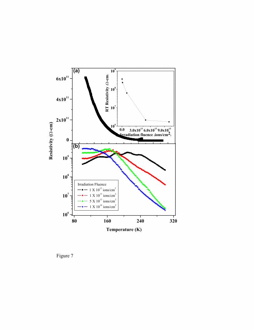
Temperature dependent resistivity measurement has been carried out for Zn0.98Mn0.02O and Zn0.96Mn0.04O
samples as shown in figure 7 and 8 respectively. For Zn0.98Mn0.02O, a monotonic decrease in RT with increasing
irradiation fluence has been observed [inset of figure 7(a)] with two orders of magnitude reduction due to highest
fluence (1×10¹⁴
ions/cm2). In a recent work, lowering of RT by four orders of magnitude has been found in 1.2
MeV Ar irradiated ZnO [34]. Huge resistance loss due to irradiation by light/heavy energetic ions has also been
observed by other groups [42]. The reason for change in resistivity due to irradiation, particularly in doped ZnO
systems, is a matter of investigation till date [17]. The decrease of resistivity is due to increase of donors or
deactivation of compensating acceptors or both. In polycrystalline samples, most of the vacancy clusters reside
near the GB region as mentioned earlier. The region is devoid of carriers (depletion region) and act as a potential
barrier during the transport of carriers between the grains. Increased donor density can reduce the height of the
potential barrier in n type ZnO. On the other hand, recovery of a fraction of GB defects can also lower the carrier
scattering at GB. At the same time, Dong et al [17] proposed that the presence of large vacancy clusters and huge
oxygen vacancies are the source of reduced resistance in ion irradiated ZnO. It should be mentioned here that,
electronic energy deposition can excite (and also ionize) the atoms and after de-excitation within few ps, a
reorganization of local defect structure is possible. This process is more effective near the highly defective
regions i.e, at the GB. We feel that resultant stable defect structure creates large oxygen vacancies (OV) as
dominant defects in ZnO based systems. Indeed, our PAL results (discussed later) reflect the existence of
vacancy cluster in the pristine Zn0.98Mn0.02O sample. However, XRD or PAL studies does not support further
clustering of vacancies due to Li ion irradiation. Hence, it can be summarized that, the recovery of a fraction of
GB defects as well as the presence of OV’s due to irradiation contribute to the reduction of resistivity in these
polycrystalline samples. The thermal variation of resistivity measurement of the irradiated Zn0.98Mn0.02O sample
shows an interesting behavior. Though the unirradiated Zn0.98Mn0.02O sample is semiconducting in nature
throughout the temperature range of measurement, but after irradiation it shows a metal to semiconductor
transition. Most interestingly, no such transition is observed in the case of Zn0.96Mn0.04O sample (all samples,
irradiated and un-irradiated, showing semiconducting behavior in the measured temperature range). Recently,
different groups reported metal-semiconductor transition in both doped and undoped ZnO system [27,21,43]. It
is noteworthy to mention that, our observation is slightly different. We observed that the sample is metallic in
low temperature regime and semiconducting in higher temperature. Also the sample irradiated with lowest
fluence shows multiple transitions but for the samples irradiated with higher fluences (1×10¹³
ions/cm2 to 1×10
14
ions/cm2), only one transition has been observed. Angadi et al [21] and Nistor et al [43] have shown that, the
presence of oxygen vacancies possibly give rise to metal-semiconductor transition in ZnO thin film. Further we
observe that the transition temperature shifts towards lower temperature with increasing doses of irradiation
[figure 7b]. Homogenization of defects with higher fluence may be responsible for the vanishing of multiple
transitions and leading towards semiconducting behavior with increasing dose of irradiation.
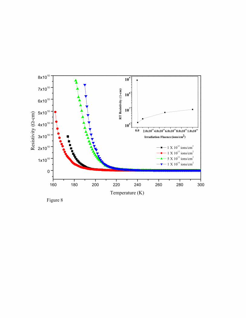
We have also investigated the resistivity of the 4 at% Mn doped sample, Zn0.96Mn0.04O. We found that
RT of the un-irradiated Zn0.96Mn0.04O sample is higher than that of 2 at% Mn doped sample. Interestingly, we
observed a two orders of magnitude reduction in RT value for the Zn0.96Mn0.04O sample with initial irradiation
fluence (1×10¹²
ions/cm2). Such reduction of RT with irradiation was also observed for Zn0.98Mn0.02O. But
unlike Zn0.98Mn0.02O, RT of the Zn0.96Mn0.04O shows a small but steady increase, as the irradiation fluence is
further increased from 1×10¹³
ions/cm2 to 1×10
14 ions/cm
2 (figure 8 (inset)). Since the Zn0.96Mn0.04O sample
contains higher percentage of Mn, the equilibrium defective state (after irradiation) of the sample is different
than that of Zn0.98Mn0.02O. As RT value is very high, we have not attempted to measure the low temperature
resistivity of the un-irradiated Zn0.96Mn0.04O sample. However, we have measured the thermal variation of
resistivity of the all the irradiated Zn0.96Mn0.04O samples (figure 8). It is noteworthy to mention that, we have
been able to measure the resistivity for these of samples only down to 170 K, below which resistivity tends
beyond the limit of the instrument. All the irradiated Zn0.96Mn0.04O samples remain semiconducting down to the
lowest temperature measured.
PAL measurements on un-irradiated and few irradiated Zn0.98Mn0.02O samples show interesting features.
The possible impurity phase related problem may complicate the PAL data for 4 at% Mn doped samples and so
the measurement for this sample is avoided. The results of PAL spectrum analysis are shown in table 1. All the
PAL spectra are found to be best fitted with three lifetime components. The longest lifetime component (
1400 ps with intensity 3-5%) originates due to the annihilation of positron from orthopositronium atoms. Decay
of orthopositronium into parapositronium through pickoff annihilation gives rise to such a large lifetime. In
polycrystalline samples, there always exist micro voids where orthopositronium formation is favourable [14]. As
the first lifetime component (1) and the intermediate one () have changed significantly with irradiation
fluence, we feel that both have defect related origin. and provide a qualitative indication about the spatial
extension of the defects (i.e, defect size). The corresponding intensities (I1 and I2 respectively) reflect the relative
abundance of such defect sites. For unirradiated sample the value of is close to the positron lifetime at zinc
vacancies in ZnO. Indeed, Wang et al [44] have attributed the origin of from the diffused zinc vacancies at the
interface of the grains. The value of indicates that there exist large vacancy clusters in the sample, possibly of

type VZn-O divacancies near the GB region [14]. High concentration of open volume defects and related disorder
can produce foam like structure near the GB as predicted by Straumel et al. [8]. Such grain boundary disorder is
drastically modified due to Li3+
irradiation. Compared to unirradiated sample, sharply decreases after initial
fluence of 1 × 10¹²
ions/cm2. RT also shows decrease with increasing irradiation fluence. This is due to formation
of increasing neutral oxygen vacancies with irradiation fluence. As decreasing trends of as well asRT with
irradiation indicate increasing presence of free electrons in the system. It is possible that a fraction of the injected
positrons are now annihilated in the bulk of the sample. So becomes closer (but lower) [45] to the bulk
lifetime of positrons in ZnO after irradiation. It is indeed an interesting observation. also shows significant
reduction due to initial dose of irradiation. Hence, we feel that there is no evidence of increase in vacancy
clusters with initial dose of irradiation. Also, we observe that, and shows a minute increase with further
irradiation fluence. However, and are fitting dependent parameters to some extent. In such complex
systems, statistically more accurate parameter is average positron lifetime, av= (I1 + I2)/(I1+I2), which
reflects the overall defective nature of the sample [14,46]. av decreases due to irradiation with 1 × 10¹²
ions/cm2
flunce and remains unaffected due to further increase of irradiation.
4. Conclusion
The un-irradiated and 50 MeV Li3+
ion irradiated Zn1-xMnxO (x = 0.02, 0.04) samples were characterized
by XRD, temperature dependent resistivity and room temperature PAL spectroscopy.
XRD result indicates wurtzite type structure for Zn0.98Mn0.02O but impurity (112) peak of ZnMn2O4 was
developed apart from usual peaks of ZnO for Zn0.96Mn0.04O. Ion irradiation dissolves the impurity phase. SEM
micrographs indicate homogeneity of the samples with uniform particle size. Room temperature resistivity
values decrease abruptly with irradiation. Generation of oxygen vacancy, Zn interstitial and recovery of a part of
defects at GB due to irradiation may be the reason of resistivity reduction. The temperature dependent electrical
resistivity results for irradiated Zn0.98Mn0.02O samples shows shifting of metal-semiconductor transition
temperature towards lower side with increasing fluence of irradiation. The RT values of the Zn0.96Mn0.04O are
higher compared to that of Zn0.98Mn0.02O samples. No metal-semiconductor transition is observed in any
irradiated Zn0.96Mn0.04O samples from the temperature dependent of resistivity measurement at least down to 170

K. PAL spectroscopy data analysis indicates that increasing fluence of irradiation cause lowering of defects in
Zn0.98Mn0.02O. This fact is also supported from XRD and electrical resistivity measurements.
Acknowledgement
The authors are thankful to IUAC, New Delhi for providing the ion beam irradiation facilities. One of
the authors (SB) is also thankful to Department of Science and Technology (DST), Govt. of India and IUAC,
New Delhi for providing financial support in the form of sanctioning research project, vide project no.:
SF/FTP/PS-31/2006 and UFUP-43308 respectively. Author SKN is thankful to University Grants Commission
(UGC) for providing him Junior Research Fellowship and author SC is grateful to Government of West Bengal
for providing financial assistance in form of University Research Fellowship.
References:
[1] Calderón M J and Sarma S D 2007 Phys. Rev. B 75 235203
[2] Stojić B B, Milivojević D, Blanuša J, Spasojević V, Bibić N, Simonović B and Arandelović D 2008 J.
Phys.: Condens. Matter 20 235217
[3] Philipose U, Nair S V, Trudel S, de Souza C F, Aouba S, Hill R H and Ruda H E 2006 Appl. Phys. Lett.
88 263101
[4] Esch A V, Boeck J D, Bockstal L V, Bogaerts R, Herlach F and Borghs G 1997 J. Phys.: Condens.
Matter 9 L361
[5] Dietl T, Ohno H, Matsukura F, Cibert J, Ferrand D 2000 Science 287 1019
[6] Sharma P, Gupta A, Rao K V, Owens F J, Sharma R, Ahuja R, Guillen J M O, Johansson B, Gehring G A
2003 Nat. Mater. 2 673
[7] Li X L, Xu X H, Quan Z Y, Guo J F, Wu H S and Gehring G A 2009 J. Appl. Phys. 105 103914
[8] Straumal B B, Mazilkin A A, Protasova S G, Myatiev A A, Straumal P B, Schütz G, van Aken P A,
Goering E and Baretzky B 2009 Phys. Rev. B 79 205206
[9] Liu H, Yang J, Zhang Y, Yang L, Wei M and Ding X 2009 J. Phys.: Condens. Matter 21 145803
[10] Behan A J, Mokhtari A, Blythe H J, Score D, Xu X-H, Neal J R, Fox A M and Gehring G A 2008 Phys.
Rev. Lett. 100 047206
Mukherjee D, Dhakal T, Srikanth H, Mukherjee P, and Witanachchi S 2010 Phys. Rev. B 81 205202
[11] García M A et al. 2005 Phys. Rev. Lett. 94 217206
[12] Coey J M D, Venkatesan M and Fitzgerald C B 2005 Nat. Mater. 4 173
[13] Zhang J, Li X Z, Shi J, Lu Y F and Sellmyer D J 2007 J. Phys.: Condens. Matter. 19 036210
[14] Dutta S, Chattopadhyay S, Sarkar A, Chakrabarti M, Sanyal D and Jana D 2009 Prog. Mater. Sc. 54
89
[15] Yi J B et al. 2010 Phys. Rev. Lett. 104 137201
[16] Chattopadhyay S, Neogi S K, Sarkar A, Mukadam M D, Yusuf S M, Banerjee A and Bandyopadhyay
S 2011 J. Magn. Magn. Mat. 323 363
[17] Dong Y, F. Tuomisto, B. G. Svensson, A. Y. Kuznetsov, L. J. Brillson, 2010 Phys. Rev. B 81 081201
[18] Tian Y F et al. 2010 J. Appl. Phys. 107 033713
Sokolov V I, Druzhinin A V, Gruzdev N B, Dejneka A, Churpita O, Hubicka Z, Jastrabik L and
Trepakov V 2010 Phys. Rev. B 81 153104
[19] Thota S, Dutta T and Kumar J 2006 J. Phys.: Condens. Matter 18 2473
[20] Kumar S, Kumar R and Singh D P 2009 Appl. Sur. Sc. 255 8014
[21] Angadi B, Jung Y S, Choi W K, Kumar R, Jeong K, Shin S W, Lee J H, Song J H, Khan M W and
Srivastava J P 2006 Appl. Phys. Lett. 88 142502
[22] Look D C, Reynolds D C, Hemsky J W, Jones R L and Sizelove J R 1999 Appl. Phys. Lett. 75 811
[23] Hayes M, Auret F D, van Rensburg P J J, Nel J M, Wesch W and Wendler E 2007 Nucl. Instru. Meth.
Phys. Res. B 257 311
[24] Zang H et al. 2008 Nucl. Instru. Meth. Phys. Res. B 266 2863
[25] Agarwal D C, Kumar A, Khan S A, Kabiraj D, Singh F, Tripathi A, Pivin J C, Chauhan R S and
Avasthi D K 2006 Nucl. Instru. Meth. Phys. Res. B 244 136
[26] Kumar P M R, Vijayakumar K P and Kartha C S 2007 J. Mater. Sci. 42 2598
[27] Kumar R, Singh A P, Thakur P, Chae K H, Choi W K, Angadi B, Kaushik S D and Patnaik S 2008 J.
Phys. D: Appl. Phys. 41 155002
[28] Fukuoka O, Matsunami N, Tazawa M, Shimura T, Sataka M, Sugai H and Okayasu O 2006 Nucl.
Instru. Meth. Phys. Res. B 250 295
[29] Sugai H, Matsunami N, Fukuoka O, Sataka M, Kato T, Okayasu O, Shimura T and Tazawa M 2006
Nucl. Instr. Meth. Phys. Res. B 250 291
[30] Kumar R et al. 2006 J. Appl. Phys. 100 113708
[31] Chattopadhyay S, Dutta S, Banerjee A, Jana D, Bandyopadhyay S, Chattopadhyay S and Sarkar A
2009 Physica B 404 1509
[32] Kirkegaard P, Pedersen N J and Eldrup M, 1089 Report of Riso National Lab Riso-M-2740
[33] Ziegler J F, Biersack J P and Littmerk U 1985 Stopping Power and Ranges of Ion in Matter (SRIM)
(New York: Pergamon Press)
Ziegler J F, Ziegler M D, Biersack J P Computer code SRIM available from http://www.SRIM.org
[34] Chattopadhyay S, Dutta S, Jana D, Chattopadhyay S, Sarkar A, Kumar P, Kanjilal D, Mishra D K and
Ray S K 2010 J. Appl. Phys. 107 113516
[35] Matsunami N, Itoh M, Takai Y, Tazawa M and Sataka M 2003 Nucl. Instru. Meth. Phys. Res. B 206
282
[36] Ramanachalam M S, Rohatgi A, Carter W B, Schaffer J P and Gupta T K 1995 J. Elect. Mat. 24 413
[37] Krishna R, Baranwal V, Katharria Y S, Kabiraj D, Tripathi A, Singh F, Khan S A, Pandey A C and
Kanjilal D 2006 Nucl. Instru. Meth. Phys. Res. B 244 78
[38] Wendler E, Bilani O, Gartner K, Wesch W, Hayes M, Auret F D , Lorenz K, and Alves E 2009 Nucl.
Instru. Meth. Phys. Res. B 267 2708
[39] Hong R , Huang J, He H, Fan Z, Shao J 2005 Appl. Sur. Sci 242 346
[40] Deshmukh A V, Patil S I, Yusuf S M, Rajarajan A K, Lalla N P 2010 J. Mag. Mag. Mat. 322 536
[41] Kelsall R W, Hamley I W, Geoghegan M, 2006 ‘Nanoscale Science and Technology’ (John
Wiley & Sons)
[42] Izawa Y, Matsumoto K, Kuriyama K and Kushida K 2010 Nucl. Instru. Meth. Phys. Res. B 268 2104
[43] Nistor M, Gherendi F, Mandache N B, Hebert C, Perrière J and Seiler W 2009 J. Appl. Phys. 106
103710
[44] Wang D, Chen Z Q, Wang D D, Qi N, Gong J, Cao C Y and Tang Z 2010 J. Appl. Phys. 107 023524
[45] Tuomisto F, Mycielski A and Grasza K 2007 Sup. latti. Microstr. 42 218
[46] Krause-Rehberg R and Leipner H S 1999 Positron Annihilation in Semiconductors (Berlin: Springer)
Figure Captions:
Figure 1: XRD of un-irradiated and irradiated 2 at% Mn doped ZnO sample.
Figure 2: XRD of un-irradiated and irradiated 4 at% Mn doped ZnO sample. Inset: Enlarge view of XRD in the
range 28o to 30
o.
Figure 3: Variation of FWHM and intensity of (101) peak with irradiation fluence for 2 at% Mn doped ZnO
sample.
Figure 4: Variation of FWHM and intensity of (101) peak with irradiation fluence for 4 at% Mn doped ZnO
sample.
Figure 5: SEM micrographs of Zn0.98 Mn0.02O samples, (a) unirradiated and (b) irradiated with fluence of 1x10¹⁴
Li3+
ions/cm2.
Figure 6: SEM micrographs of Zn0.96 Mn0.04O samples, (a) unirradiated and (b) irradiated with fluence of 1x10¹⁴
Li3+
ions/cm2.
Figure 7: (a) Thermal variation resistivity of un-irradiated Zn0.98Mn0.02O sample. Inset: Variation of RT of
Zn0.98Mn0.02O with irradiation irradiation fluence. (b) Thermal variation resistivity of all irradiated Zn0.98Mn0.02O
sample.
Figure 8: Thermal variation resistivity of all irradiated Zn0.96Mn0.04O sample. Inset: Variation of RT of
Zn0.96Mn0.04O with irradiation fluence.
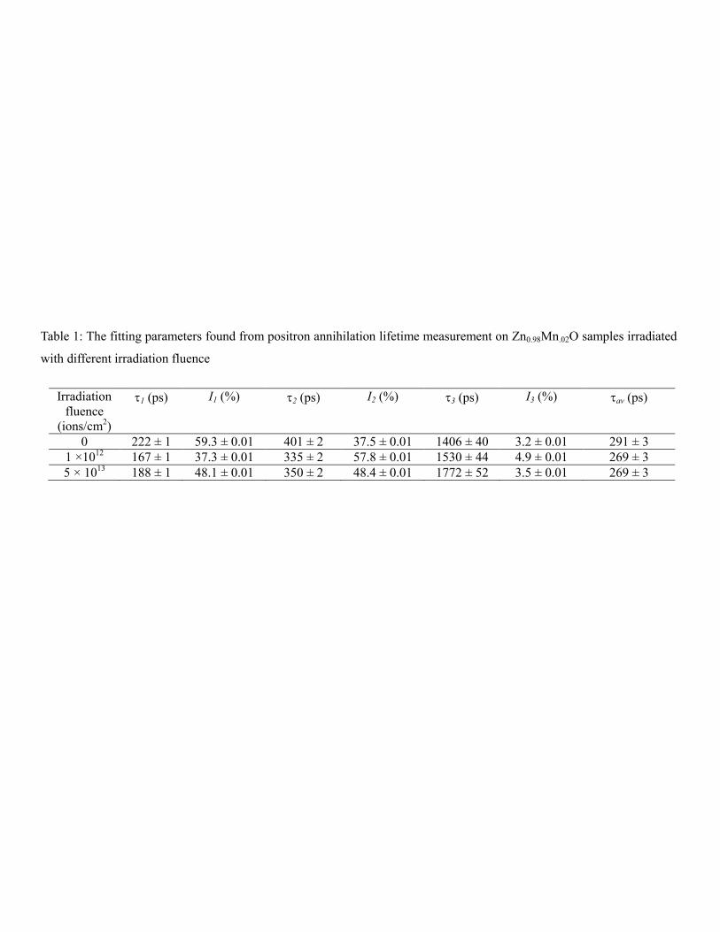
Table 1: The fitting parameters found from positron annihilation lifetime measurement on Zn0.98Mn.02O samples irradiated
with different irradiation fluence
Irradiation
fluence
(ions/cm2)
1 (ps) I1 (%) 2 (ps) I2 (%) 3 (ps) I3 (%) av (ps)
0 222 ± 1 59.3 ± 0.01 401 ± 2 37.5 ± 0.01 1406 ± 40 3.2 ± 0.01 291 ± 3
1 ×10¹²
167 ± 1 37.3 ± 0.01 335 ± 2 57.8 ± 0.01 1530 ± 44 4.9 ± 0.01 269 ± 3
5 × 10¹³
188 ± 1 48.1 ± 0.01 350 ± 2 48.4 ± 0.01 1772 ± 52 3.5 ± 0.01 269 ± 3
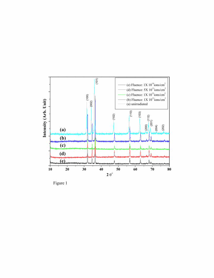
10 20 30 40 50 60 70 80
(e)
(d)
(c)
(a)
Inte
nsi
ty (
Arb
. U
nit
)
2
(e) Fluence: 1X 10¹⁴
ions/cm2
(d) Fluence: 5X 10¹³
ions/cm2
(c) Fluence: 1X 10¹³
ions/cm2
(b) Fluence: 1X 10¹²
ions/cm2
(a) unirradiated
(b)
(100
)(0
02)
(101
)
(102
)
(110
)
(103
)
(200
)(1
12)
(201
)
(004
)
(202
)
Figure 1
10 20 30 40 50 60 70 80
28.0 28.4 28.8 29.2 29.6 30.0
(112
) of
ZnM
n 2O
4
(e)(d)(c)(b)
Inte
nsi
ty (
Arb
. Un
it)
2
Unirradiated
Fluence: 1 X 10¹²
ions/cm2
Fluence: 1 X 10¹³
ions/cm2
Fluence: 5 X 10¹³
ions/cm2
Fluence: 1 X 10¹⁴
ions/cm2
(a)
(100
)
(002
)(1
01)
(102
)
(110
)
(103
)
(200
)(1
12)
(201
)
(004
)
(202
)
(100
)(0
02)
(101
)
(102
)
(110
)
(103
)
(200
)(1
12)
(201
)
(004
)
(202
)
Inte
nsi
ty (
Arb
. Un
it)
2
Figure 2
0.19
0.20
0.21
0.22
0.23
0.24
0.25
0 20 40 60 80 100
600
800
1000
1200
1400
1600
1800
2000
2200
FWH
M o
f (10
1) P
eak
(0 )
FWHM of (101) Peak
Inte
nsi
ty o
f (1
01)
Peak
(A
rb
. U
nit
)
Irradiation Fluence (X 1012
ions/cm2)
Intensity of (101) Peak
Figure 3
0.21
0.22
0.23
0.24
0.25
0.26
0 20 40 60 80 100
700
800
900
1000
1100
1200
1300
1400
1500 FWHM of (101) Peak
FWHM
of (
101)
Pea
k (0 )
Intensity of (101) Peak
Inte
nsi
ty o
f (1
01
) P
eak
(A
rb.
Un
it)
Irradiation Fluence (X 1012
ions/cm2)
Figure 4
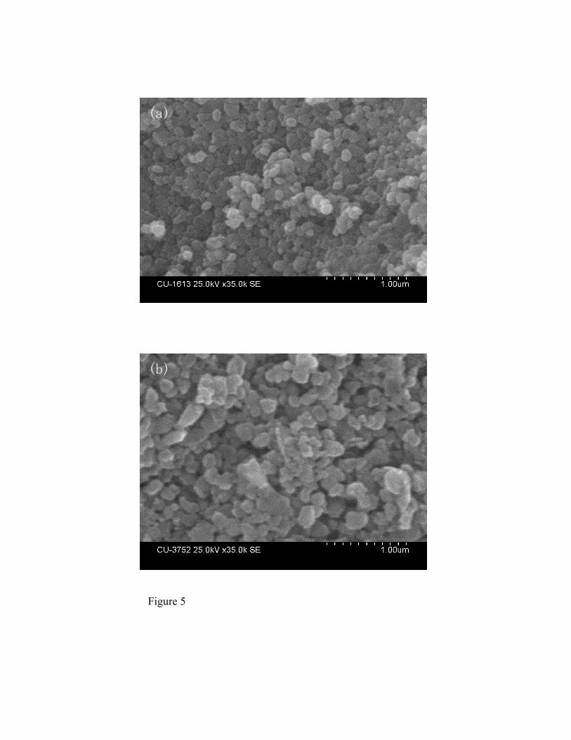
Figure 5
(b)
(a)
Figure 5
(b)
(a)

(a)
(b)
Figure 6
0
2x10¹¹
4x10¹¹
6x10¹¹
80 160 240 320
106
107
108
109
0.0 3.0x10¹³
6.0x10¹³
9.0x10¹³
106
107
108
109
(b)
Res
isti
vit
y (
-cm
)
(a)
Irradiation Fluence
1 X 10¹²
ions/cm2
1 X 10¹³
ions/cm2
5 X 10¹³
ions/cm2
1 X 10¹⁴
ions/cm2
Temperature (K)
RT
Res
isti
vit
y (
-cm
)
Irradiation fluence (ions/cm2)
Figure 7
160 180 200 220 240 260 280 300
0
1x10¹⁰
2x10¹⁰
3x10¹⁰
4x10¹⁰
5x10¹⁰
6x10¹⁰
7x10¹⁰
8x10¹⁰
0.0 2.0x10¹³
4.0x10¹³
6.0x10¹³
8.0x10¹³
1.0x10¹⁴
106
107
108
109
Res
isti
vit
y (
-cm
)
Temperature (K)
1 X 10¹²
ions/cm2
1 X 10¹³
ions/cm2
5 X 10¹³
ions/cm2
1 X 10¹⁴
ions/cm2
RT
Resi
stiv
ity
-cm
)
Irradiation Fluence (ions/cm2)
Figure 8
Related Documents