IRAMS06UP60A Series 6A, 600V www.irf.com 1 Features • Integrated Gate Drivers and Bootstrap Diodes • Temperature Monitor • Overcurrent shutdown • Fully Isolated Package. • Low V CE(on) Non Punch Through IGBT Technology • Undervoltage lockout for all channels • Matched propagation delay for all channels • Schmitt-triggered input logic • Cross-conduction prevention logic • Lower di/dt gate driver for better noise immunity • Motor Power range 0.1~0.5kW / 85~253 Vac • Isolation 2000V RMS /1min Plug N Drive TM Integrated Power Module for Appliance Motor Drive Description International Rectifier’s IRAMS06UP60A is an Integrated Power Module developed and optimized for electronic motor control in appliance applications specifically for VF compressor drives for refrigerators and freezer or in heating and ventilation as electronic fan controls. The IRAMS06UP60A offers an extremely compact, high performance AC motor-driver in a single isolated package for a very simple design. A built-in temperature monitor and over-current protection, along with the short-circuit rated IGBTs and integrated under-voltage lockout function, deliver high level of protection and fail-safe operation. The integration of the bootstrap diodes for the high-side driver section, and the single polarity power supply required to drive the internal circuitry, simplify the utilization of the module and deliver further cost reduction advantages. PD-95831 RevB Absolute Maximum Ratings Parameter Description Max. Value Units V CES Maximum IGBT Blocking Voltage 600 V + Positive Bus Input Voltage 450 I o @ T C =25°C RMS Phase Current 6 I o @ T C =100°C RMS Phase Current 3 I pk Maximum Peak Phase Current (tp<100ms) 10 F p Maximum PWM Carrier Frequency 20 kHz P d Maximum Power dissipation per Phase 7.5 W V iso Isolation Voltage (1min) 2000 V RMS T J (IGBT & Diodes) Operating Junction temperature Range -40 to +150 T J (Driver IC) Operating Junction temperature Range -40 to +150 T Mounting torque Range (M3 screw) 0.8 to 1.0 Nm A °C V

Welcome message from author
This document is posted to help you gain knowledge. Please leave a comment to let me know what you think about it! Share it to your friends and learn new things together.
Transcript

IRAMS06UP60ASeries
6A, 600V
www.irf.com 1
Features• Integrated Gate Drivers and Bootstrap Diodes• Temperature Monitor• Overcurrent shutdown• Fully Isolated Package.• Low VCE(on) Non Punch Through IGBT
Technology• Undervoltage lockout for all channels• Matched propagation delay for all channels• Schmitt-triggered input logic• Cross-conduction prevention logic• Lower di/dt gate driver for better noise immunity• Motor Power range 0.1~0.5kW / 85~253 Vac• Isolation 2000VRMS /1min
Plug N DriveTM Integrated PowerModule for Appliance Motor Drive
DescriptionInternational Rectifier’s IRAMS06UP60A is an Integrated Power Module developed and optimized forelectronic motor control in appliance applications specifically for VF compressor drives for refrigerators andfreezer or in heating and ventilation as electronic fan controls. The IRAMS06UP60A offers an extremelycompact, high performance AC motor-driver in a single isolated package for a very simple design.A built-in temperature monitor and over-current protection, along with the short-circuit rated IGBTs andintegrated under-voltage lockout function, deliver high level of protection and fail-safe operation.The integration of the bootstrap diodes for the high-side driver section, and the single polarity powersupply required to drive the internal circuitry, simplify the utilization of the module and deliver furthercost reduction advantages.
PD-95831 RevB
Absolute Maximum Ratings
Parameter Description Max. Value Units
VCES Maximum IGBT Blocking Voltage 600
V+ Positive Bus Input Voltage 450
Io @ TC=25°C RMS Phase Current 6
Io @ TC=100°C RMS Phase Current 3
Ipk Maximum Peak Phase Current (tp<100ms) 10
Fp Maximum PWM Carrier Frequency 20 kHz
Pd Maximum Power dissipation per Phase 7.5 W
Viso Isolation Voltage (1min) 2000 VRMS
TJ (IGBT & Diodes) Operating Junction temperature Range -40 to +150
TJ (Driver IC) Operating Junction temperature Range -40 to +150
T Mounting torque Range (M3 screw) 0.8 to 1.0 Nm
A
°C
V

IRAMS06UP60A
2 www.irf.com
Internal Electrical Schematic - IRAMS06UP60A
23 VS1
24 HO1
25 VB1
1 VCC
2 HIN1
3 HIN2
4 HIN3
5 LIN1LIN2
6LIN3
7F8
ITRIP9
EN10
RCIN11
VSS12
COM13
22VB2
21HO2
20VS2
19VB3
18HO3
17VS3
VRU (12)
VRW (14)
VRV (13)
VB1 (7)U, VS1 (8)
VB2 (4)V, VS2 (5)
VB3 (1)W, VS3 (2)
THERMISTOR
R3
VDD (22)
VSS (23)
R1
R2
C
Rg1 Rg3 Rg5
Driver IC
RT
LO1 16
LO3 14
LO2 15
Rg2
Rg4
Rg6
T/ITRIP (21)
HIN1 (15)HIN2 (16)HIN3 (17)
LIN1 (18)
LIN2 (19)
LIN3 (20)
V (10)+

IRAMS06UP60A
www.irf.com 3
Inverter Section Switching Characteristics @ TJ = 25°C
Thermal Resistance
Inverter Section Electrical Characteristics @ TJ = 25°C
Symbol Parameter Min Typ Max Units
Eon Turn-On Switching Loss --- 130 235
Eoff Turn-Off Switching Loss --- 65 120
Etot Total Switching Loss --- 195 355 TJ=25°C
Eon Turn-on Swtiching Loss --- 200 345 TJ=150°C
Eoff Turn-off Switching Loss --- 90 150
Etot Total Switching Loss --- 290 495
ErecDiode Reverse Recovery energy
--- 50 110 µJ
trr Diode Reverse Recovery time --- 150 200 ns
RBSOAReverse Bias Safe Operating Area
SCSOAShort Circuit Safe Operating Area
10 --- --- µsTJ=150°C, VP=600V,V+=360V,VDD=+15V to 0V See CT2
µJ
µJ
TJ=150°C, V+ =400V VDD=15V, IF=3A, L=1mH
FULL SQUARETJ=150°C, IC=3A, VP=600VV+=480V, VDD=+15V to 0V See CT3
Conditions
IC=3A, V+=400VVDD=15V, L=1mH
See CT1
Energy losses include "tail" and diode reverse recovery
Symbol Parameter Min Typ Max Units Conditions
Rth(J-C)
Junction to case thermal resistance, each IGBT under inverter operation.
--- --- 6.5 °C/W
Rth(J-C)
Junction to case thermal resistance, each Diode under inverter operation.
--- --- 9 °C/W
Rth(C-S)Thermal Resistance case to sink
--- 0.1 --- °C/W
Flat, greased surface. Heatsink compound thermal conductivity - 1W/mK
Symbol Parameter Min Typ Max Units Conditions
V(BR)CESCollector-to-Emitter Breakdown Voltage
600 --- --- V VIN=5V, IC=250µA
∆V(BR)CES / ∆TTemperature Coeff. Of Breakdown Voltage
--- 0.3 --- V/°CVIN=5V, IC=1.0mA(25°C - 150°C)
--- 1.9 2.4 IC=3A, VDD=15V
--- 2.2 2.6 IC=3A, VDD=15V, TJ=150°C
--- 15 45 VIN=5V, V+=600V
--- 60 170 VIN=5V, V+=600V, TJ=150°C
Ilk_moduleZero Gate Voltage Phase-to-phase Current
-- -- 50 µA VIN=5V, V+=600V
--- 1.45 1.85 IC=3A
--- 1.25 1.65 IC=3A, TJ=150°C
V
µA
V
VCE(ON)
ICES
VFM
Collector-to-Emitter Saturation Voltage
Zero Gate Voltage Collector-to-Emitter Current
Diode Forward Voltage Drop
IRAMS06UP60A
4 www.irf.com
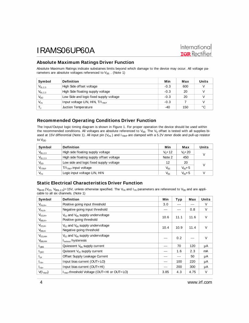
Static Electrical Characteristics Driver FunctionVBIAS (VCC, VBS1,2,3)=15V, unless otherwise specified. The VIN and IIN parameters are referenced to VSS and are appli-cable to all six channels. (Note 1)
Recommended Operating Conditions Driver FunctionThe Input/Output logic timing diagram is shown in Figure 1. For proper operation the device should be used withinthe recommended conditions. All voltages are absolute referenced to VSS. The VS offset is tested with all supplies bi-ased at 15V differential (Note 1). All input pin (VIN ) and ITRIP are clamped with a 5.2V zener diode and pull-up resistorto VDD
Absolute Maximum Ratings Driver FunctionAbsolute Maximum Ratings indicate substaines limits beyond which damage to the device may occur. All voltage pa-rameters are absolute voltages referenced to . (Note 1)VSS
14
Symbol Definition Min Max UnitsVS1,2,3 High Side offset voltage -0.3 600 V
VB1,2,3 High Side floating supply voltage -0.3 20 V
VDD Low Side and logic fixed supply voltage -0.3 20 V
VIN Input voltage LIN, HIN, T/ITRIP -0.3 7 V
TJ Juction Temperature -40 150 °C
Symbol Definition Min Max UnitsVB1,2,3 High side floating supply voltage VS+12 VS+20
VS1,2,3 High side floating supply offset voltage Note 2 450
VDD Low side and logic fixed supply voltage 12 20
VITRIP T/ITRIP input voltage VSS VSS+5
VIN Logic input voltage LIN, HIN VSS VSS+5 V
V
V
Symbol Definition Min Typ Max UnitsVIN,th+ Positive going input threshold 3.0 --- --- V
VIN,th- Negative going input threshold --- --- 0.8 V
IQBS Quiescent VBS supply current --- 70 120 µA
IQCC Quiscent VCC supply current --- 1.6 2.3 mA
ILK Offset Supply Leakage Current --- --- 50 µA
IIN+ Input bias current (OUT=LO) --- 100 220 µA
IIN+ Input bias current (OUT=HI) --- 200 300 µA
V(ITRIP) ITRIP threshold Voltage (OUT=HI or OUT=LO) 3.85 4.3 4.75 V
11.4
---
V
V
V
10.9
0.2
10.4
---
VCCUV+
VBSUV+
VCCUV-
VBSUV-
VCC and VBS supply undervoltageNegative going threshold
VCCUVH
VBSUVH
VCC and VBS supply undervoltageIlockout hysteresis
10.6 11.1 11.6VCC and VBS supply undervoltagePositive going threshold

IRAMS06UP60A
www.irf.com 5
Note 3: The Maximum recommended sense voltage at the T/ITRIP terminal under normal operating conditions is 3.3V.
Internal NTC - Thermistor Characteristics
Note 1: For more details, see IR21365 data sheet
Note 2: Logic operational for Vs from V- -5V to V- +600V. Logic state held for Vs from V- -5V to V- -VBS. (please refer toDT97-3 for more details)
Dynamic Electrical CharacteristicsVDD=VBS=VBIAS=15V, Io=1A, VD=9V, PWMIN=2kHz, VIN_ON=VIN_th+, VIN_OFF=VIN_th-
TA=25°C, unless otherwise specified
Thermistor Built-in IRAMS06UP60A
IR2136512K
NTC
VCC (22)
T/ITRIP (21)
VSS (23)6.8k
Typ Units Conditions
R25 Resistance 100 +/- 3% kΩ TC = 25°C
R125 Resistance 2.522 + 17.3 % /- 14.9% kΩ TC = 125°C
B B-constant (25-50°C) 4250 +/- 2% k R2 = R1e [B(1/T2 - 1/T1)]
-40 / 125 °C
1 mW/°C TC = 25°C
Parameter
Temperature Range
Typ. Dissipation constant
Symbol Definition Min Typ Max Units
TON Input to output propagation turn-on delay time (see fig.11) - 470 - ns
TOFF Input to output propagation turn-off delay time (see fig. 11) - 615 - ns
DT Dead Time - 290 - ns
I/TTrip T/ITrip to six switch to turn-off propagation delay (see fig. 2) - 750 - ns
TFCLTRL Post ITrip to six switch to turn-off clear time (see fig. 2) - 9 - ms

IRAMS06UP60A
6 www.irf.com
Figure1. Input/Output Timing Diagram
Note 5: The shaded area indicates that both high-side and low-side switches are off and therefore the half-bridge outputvoltage would be determined by the direction of current flow in the load.
Ho
Lo
U,V,WIC
Driver
V+
Hin1,2,3
Lin1,2,3
(15,16,17)
(18,19,20)
(8,5,2)
Itrip U,V,W
0 0 1 V+0 1 0 00 1 1 X1 X X X
HIN1,2,3 LIN1,2,3
HO1,2,3
LO1,2,3
Itrip
U,V,W
HIN1,2,3
LIN1,2,3

IRAMS06UP60A
www.irf.com 7
Note 6: The shaded area indicates that both high-side and low-side switches are off and therefore the half-bridge outputvoltage would be determined by the direction of current flow in the load.
Figure 2. ITrip Timing Waveform
T/Itrip
LIN1,2,3
HIN1,2,3
tfltclr
50%
50%U,V,W

IRAMS06UP60A
8 www.irf.com
Module Pin-Out Description
Pin Name Description
1 VB3 High Side Floating Supply Voltage 3
2 W,VS3 Output 3 - High Side Floating Supply Offset Voltage
3 na none
4 VB2 High Side Floating Supply voltage 2
5 V,VS2 Output 2 - High Side Floating Supply Offset Voltage
6 na none
7 VB1 High Side Floating Supply voltage 1
8 U,VS1 Output 1 - High Side Floating Supply Offset Voltage
9 na none
10 V+ Positive Bus Input Voltage
11 na none
12 LE1 Low Side Emitter Connection - Phase 1
13 LE2 Low Side Emitter Connection - Phase 2
14 LE3 Low Side Emitter Connection - Phase 3
15 HIN1 Logic Input High Side Gate Driver - Phase 1
16 HIN2 Logic Input High Side Gate Driver - Phase 2
17 HIN3 Logic Input High Side Gate Driver - Phase 3
18 LIN1 Logic Input Low Side Gate Driver - Phase 1
19 LIN2 Logic Input Low Side Gate Driver - Phase 2
20 LIN3 Logic Input Low Side Gate Driver - Phase 3
21 T/Itrip Temperature Monitor and Shut-down Pin
22 VCC +15V Main Supply
23 VSS Negative Main Supply

IRAMS06UP60A
www.irf.com 9
1. Electrolytic bus capacitors should be mounted as close to the module bus terminals as possible to reduce ringing andEMI problems. Additional high frequency ceramic capacitor mounted close to the module pins will further improve perfor-mance.
2. In order to provide good decoupling between VCC-Gnd and VB-VSS terminals, the capacitors shown connected be-tween these terminals should be located very close to the module pins. Additional high frequency capacitors, typically0.1mF, are strongly recommended.
3. Value of the boot-strap capacitors depends upon the switching frequency. Their selection should be made based onIR design tip DN 98-2a, application note AN-1044 or Figure 9.
4. Low inductance shunt resistors shuld be used for phase leg current sensing. Similarly, the length of the traces be-tween pins 12, 13 and 14 to the corresponding shunt resistors should be kept as small as possible.
5. Over-current sense signal can be obtained from external hardware detecting excessive instantaneous current ininverter.
Typical Application Connection IRAMS06UP60A
VDD(15 V)
T/ITRIP
VSS3.3 V NTC12k
5k
1m
CONTROLLER
3-ph ACMOTOR
LINW
HINW
LINU
LINV
LeW
HINU
HINV
LeU
LeV
V+
VSU
VBU
VSV
VBV
VSW
VBW
Driver IC
DC BUSCAPACITORS
PHASE LEGCURRENT
SENSE
TEMPSENSE
BOOT-STRAPCAPACITORS
O/CSENSE
(ACTIVE LOW)
10m
6.8K
10.2k
U
V
WCURRENT SENSING CAN USE ASINGLE SENSE RESISTOR OR PHASE
LEG SENSING AS SHOWN
0.1m

IRAMS06UP60A
10 www.irf.com
Figure 3. Maximum sinusoidal phase current as function of switching frequency
V+=400V, Tj=150°C, Modulation Depth=0.8, PF=0.6
Figure 4. Maximum sinusoidal phase current as function of modulation frequency
V+=400V, Tj=150°C, Tc=100°C, Modulation Depth=0.8, PF=0.6
0.0
0.5
1.0
1.5
2.0
2.5
3.0
3.5
4.0
4.5
5.0
0 2 4 6 8 10 12 14 16 18 20
Switching frequency (kHz)
Max
imum
RM
S O
utpu
t Cu
rren
t/Ph
ase
(A) .
Tc= 100°CTc= 110°CTc= 120°C
0.0
0.5
1.0
1.5
2.0
2.5
3.0
3.5
4.0
1 10 100
Modulation frequency (Hz)
Max
imum
RM
S O
utpu
t Cu
rren
t/Ph
ase
(A) . 12 kHz
16 kHz
20 kHz

IRAMS06UP60A
www.irf.com 11
Figure 5. IGBT Turn-on. Typical turn-on waveform @Tj=125°C, V+=400V
Figure 6. IGBT Turn-off. Typical turn-off waveform @Tj=125°C, V+=400V
-1
0
1
2
3
4
5
6
7
8
9
0.000 0.100 0.200 0.300 0.400 0.500 0.600 0.700 0.800 0.900 1.000
Time (µs)
Curr
ent
(A)
-50
0
50
100
150
200
250
300
350
400
450
Volta
ge (
V)
CurrentVoltage
-0.5
0
0.5
1
1.5
2
2.5
3
3.5
4
4.5
0.000 0.100 0.200 0.300 0.400 0.500 0.600 0.700 0.800 0.900 1.000
Time (µs)
Curr
ent
(A)
-50
0
50
100
150
200
250
300
350
400
450
Volta
ge (
V)
CurrentVoltage

IRAMS06UP60A
12 www.irf.com
Figure 7. Variation of thermistor resistance with temperature
1
10
100
1000
0 20 40 60 80 100 120 140Temperature (°C)
Ther
imst
or R
esis
tanc
e (k
Ω)
.
Maximum
Nominal
Minimum

IRAMS06UP60A
www.irf.com 13
Figure 9. Recommended minimum Bootstrap Capacitor value Vs Switching Frequency
Figure 8. Estimated maximum IGBT junction temperature with thermistor tempera-ture
4.7
15
1.51
0
2.5
5
7.5
10
12.5
15
17.5
20
0 5 10 15 20Frequency (kHz)
Capa
cita
nce
( µF)
6.8
3.32.2
80
90
100
110
120
130
140
150
160
170
180
60 70 80 90 100 110 120Thermistor temperature (°C)
IGBT
Jun
ctio
n te
mpe
ratu
re (
°C)
Vbus=400VImot=3Armsfsw=20kHz

IRAMS06UP60A
14 www.irf.com
Figure 11. Switching Parameter Definitions
Figure 11a. Input to Output propagationturn-on delay time
Figure 11b. Input to Outputpropagation turn-off delay time
Figure 11c. Diode Reverse Recovery
VCE
IF
HIN/LIN
trr
Irr
VCE IC
HIN/LIN
TON tr
50%HIN/LIN
90% IC
10% IC
50%HIN/LIN
VCEIC
HIN/LIN
TOFF tf
90% IC
10% IC
10%VCE

IRAMS06UP60A
www.irf.com 15
Figure CT1. Switching Loss Circuit
Figure CT2. S.C.SOA Circuit
Ho
Lo
U,V,WIC
Driver
V+
Lin1,2,3
5V
Hin1,2,3
IN
Io
PWM=4µs
Ho
Lo
U,V,WIC
Driver
V+
Lin1,2,3
Hin1,2,3
IN
10k1k
5VZD
VCC
Io
Figure CT3. R.B.SOA Circuit
IN
Io
Ho
Lo
U,V,WIC
Driver
V+
Lin1,2,3
Hin1,2,3
IN
10k1k
5VZD
VCC
Io
VP=Peak Voltage on the IGBT die
VP=Peak Voltage on the IGBT die

IRAMS06UP60A
16 www.irf.com
Standard pin leadforming option
Notes:Dimensions in mm
1- Marking for pin 1 identification2- Product Part Number3- Lot and Date code marking
For mounting instruction, see AN1049
Package Outline
027-E2D24
IRAMS06UP60A
note 1
note 2
note 3

IRAMS06UP60A
www.irf.com 17
IR WORLD HEADQUARTERS: 233 Kansas St., El Segundo, California 90245, USA Tel: (310) 252-7105TAC Fax: (310) 252-7903
Visit us at www.irf.com for sales contact information09/04
Package Outline
Pin leadforming option -2
Notes:
Dimensions in mm1- Marking for pin 1 identification2- Product Part Number
3- Lot and Date code marking
Data and Specifications are subject to change without notice
027-E2D24
note 1
IRAMS06UP60A-2
note 2note 3

Related Documents


